EP2043142A1 - Mounting method using thermocompression head - Google Patents
Mounting method using thermocompression head Download PDFInfo
- Publication number
- EP2043142A1 EP2043142A1 EP07790938A EP07790938A EP2043142A1 EP 2043142 A1 EP2043142 A1 EP 2043142A1 EP 07790938 A EP07790938 A EP 07790938A EP 07790938 A EP07790938 A EP 07790938A EP 2043142 A1 EP2043142 A1 EP 2043142A1
- Authority
- EP
- European Patent Office
- Prior art keywords
- electric component
- thermocompression
- head
- adhesive agent
- mounting
- Prior art date
- Legal status (The legal status is an assumption and is not a legal conclusion. Google has not performed a legal analysis and makes no representation as to the accuracy of the status listed.)
- Granted
Links
Images


Classifications
-
- H—ELECTRICITY
- H05—ELECTRIC TECHNIQUES NOT OTHERWISE PROVIDED FOR
- H05K—PRINTED CIRCUITS; CASINGS OR CONSTRUCTIONAL DETAILS OF ELECTRIC APPARATUS; MANUFACTURE OF ASSEMBLAGES OF ELECTRICAL COMPONENTS
- H05K3/00—Apparatus or processes for manufacturing printed circuits
- H05K3/30—Assembling printed circuits with electric components, e.g. with resistors
- H05K3/32—Assembling printed circuits with electric components, e.g. with resistors electrically connecting electric components or wires to printed circuits
-
- H—ELECTRICITY
- H05—ELECTRIC TECHNIQUES NOT OTHERWISE PROVIDED FOR
- H05K—PRINTED CIRCUITS; CASINGS OR CONSTRUCTIONAL DETAILS OF ELECTRIC APPARATUS; MANUFACTURE OF ASSEMBLAGES OF ELECTRICAL COMPONENTS
- H05K3/00—Apparatus or processes for manufacturing printed circuits
- H05K3/30—Assembling printed circuits with electric components, e.g. with resistors
- H05K3/32—Assembling printed circuits with electric components, e.g. with resistors electrically connecting electric components or wires to printed circuits
- H05K3/328—Assembling printed circuits with electric components, e.g. with resistors electrically connecting electric components or wires to printed circuits by welding
-
- B—PERFORMING OPERATIONS; TRANSPORTING
- B30—PRESSES
- B30B—PRESSES IN GENERAL
- B30B15/00—Details of, or accessories for, presses; Auxiliary measures in connection with pressing
- B30B15/06—Platens or press rams
- B30B15/065—Press rams
-
- B—PERFORMING OPERATIONS; TRANSPORTING
- B30—PRESSES
- B30B—PRESSES IN GENERAL
- B30B5/00—Presses characterised by the use of pressing means other than those mentioned in the preceding groups
- B30B5/02—Presses characterised by the use of pressing means other than those mentioned in the preceding groups wherein the pressing means is in the form of a flexible element, e.g. diaphragm, urged by fluid pressure
-
- H—ELECTRICITY
- H10—SEMICONDUCTOR DEVICES; ELECTRIC SOLID-STATE DEVICES NOT OTHERWISE PROVIDED FOR
- H10W—GENERIC PACKAGES, INTERCONNECTIONS, CONNECTORS OR OTHER CONSTRUCTIONAL DETAILS OF DEVICES COVERED BY CLASS H10
- H10W72/00—Interconnections or connectors in packages
-
- H—ELECTRICITY
- H05—ELECTRIC TECHNIQUES NOT OTHERWISE PROVIDED FOR
- H05K—PRINTED CIRCUITS; CASINGS OR CONSTRUCTIONAL DETAILS OF ELECTRIC APPARATUS; MANUFACTURE OF ASSEMBLAGES OF ELECTRICAL COMPONENTS
- H05K2201/00—Indexing scheme relating to printed circuits covered by H05K1/00
- H05K2201/10—Details of components or other objects attached to or integrated in a printed circuit board
- H05K2201/10613—Details of electrical connections of non-printed components, e.g. special leads
- H05K2201/10621—Components characterised by their electrical contacts
- H05K2201/10674—Flip chip
-
- H—ELECTRICITY
- H05—ELECTRIC TECHNIQUES NOT OTHERWISE PROVIDED FOR
- H05K—PRINTED CIRCUITS; CASINGS OR CONSTRUCTIONAL DETAILS OF ELECTRIC APPARATUS; MANUFACTURE OF ASSEMBLAGES OF ELECTRICAL COMPONENTS
- H05K2201/00—Indexing scheme relating to printed circuits covered by H05K1/00
- H05K2201/10—Details of components or other objects attached to or integrated in a printed circuit board
- H05K2201/10613—Details of electrical connections of non-printed components, e.g. special leads
- H05K2201/10954—Other details of electrical connections
- H05K2201/10977—Encapsulated connections
-
- H—ELECTRICITY
- H05—ELECTRIC TECHNIQUES NOT OTHERWISE PROVIDED FOR
- H05K—PRINTED CIRCUITS; CASINGS OR CONSTRUCTIONAL DETAILS OF ELECTRIC APPARATUS; MANUFACTURE OF ASSEMBLAGES OF ELECTRICAL COMPONENTS
- H05K2203/00—Indexing scheme relating to apparatus or processes for manufacturing printed circuits covered by H05K3/00
- H05K2203/11—Treatments characterised by their effect, e.g. heating, cooling, roughening
- H05K2203/1189—Pressing leads, bumps or a die through an insulating layer
-
- H—ELECTRICITY
- H05—ELECTRIC TECHNIQUES NOT OTHERWISE PROVIDED FOR
- H05K—PRINTED CIRCUITS; CASINGS OR CONSTRUCTIONAL DETAILS OF ELECTRIC APPARATUS; MANUFACTURE OF ASSEMBLAGES OF ELECTRICAL COMPONENTS
- H05K3/00—Apparatus or processes for manufacturing printed circuits
- H05K3/30—Assembling printed circuits with electric components, e.g. with resistors
- H05K3/303—Assembling printed circuits with electric components, e.g. with resistors with surface mounted components
- H05K3/305—Affixing by adhesive
-
- H—ELECTRICITY
- H10—SEMICONDUCTOR DEVICES; ELECTRIC SOLID-STATE DEVICES NOT OTHERWISE PROVIDED FOR
- H10W—GENERIC PACKAGES, INTERCONNECTIONS, CONNECTORS OR OTHER CONSTRUCTIONAL DETAILS OF DEVICES COVERED BY CLASS H10
- H10W72/00—Interconnections or connectors in packages
- H10W72/071—Connecting or disconnecting
- H10W72/0711—Apparatus therefor
-
- H—ELECTRICITY
- H10—SEMICONDUCTOR DEVICES; ELECTRIC SOLID-STATE DEVICES NOT OTHERWISE PROVIDED FOR
- H10W—GENERIC PACKAGES, INTERCONNECTIONS, CONNECTORS OR OTHER CONSTRUCTIONAL DETAILS OF DEVICES COVERED BY CLASS H10
- H10W72/00—Interconnections or connectors in packages
- H10W72/071—Connecting or disconnecting
- H10W72/0711—Apparatus therefor
- H10W72/07141—Means for applying energy, e.g. ovens or lasers
-
- H—ELECTRICITY
- H10—SEMICONDUCTOR DEVICES; ELECTRIC SOLID-STATE DEVICES NOT OTHERWISE PROVIDED FOR
- H10W—GENERIC PACKAGES, INTERCONNECTIONS, CONNECTORS OR OTHER CONSTRUCTIONAL DETAILS OF DEVICES COVERED BY CLASS H10
- H10W72/00—Interconnections or connectors in packages
- H10W72/071—Connecting or disconnecting
- H10W72/072—Connecting or disconnecting of bump connectors
- H10W72/07251—Connecting or disconnecting of bump connectors characterised by changes in properties of the bump connectors during connecting
-
- H—ELECTRICITY
- H10—SEMICONDUCTOR DEVICES; ELECTRIC SOLID-STATE DEVICES NOT OTHERWISE PROVIDED FOR
- H10W—GENERIC PACKAGES, INTERCONNECTIONS, CONNECTORS OR OTHER CONSTRUCTIONAL DETAILS OF DEVICES COVERED BY CLASS H10
- H10W72/00—Interconnections or connectors in packages
- H10W72/071—Connecting or disconnecting
- H10W72/073—Connecting or disconnecting of die-attach connectors
-
- H—ELECTRICITY
- H10—SEMICONDUCTOR DEVICES; ELECTRIC SOLID-STATE DEVICES NOT OTHERWISE PROVIDED FOR
- H10W—GENERIC PACKAGES, INTERCONNECTIONS, CONNECTORS OR OTHER CONSTRUCTIONAL DETAILS OF DEVICES COVERED BY CLASS H10
- H10W72/00—Interconnections or connectors in packages
- H10W72/071—Connecting or disconnecting
- H10W72/073—Connecting or disconnecting of die-attach connectors
- H10W72/07331—Connecting techniques
-
- H—ELECTRICITY
- H10—SEMICONDUCTOR DEVICES; ELECTRIC SOLID-STATE DEVICES NOT OTHERWISE PROVIDED FOR
- H10W—GENERIC PACKAGES, INTERCONNECTIONS, CONNECTORS OR OTHER CONSTRUCTIONAL DETAILS OF DEVICES COVERED BY CLASS H10
- H10W72/00—Interconnections or connectors in packages
- H10W72/20—Bump connectors, e.g. solder bumps or copper pillars; Dummy bumps; Thermal bumps
-
- H—ELECTRICITY
- H10—SEMICONDUCTOR DEVICES; ELECTRIC SOLID-STATE DEVICES NOT OTHERWISE PROVIDED FOR
- H10W—GENERIC PACKAGES, INTERCONNECTIONS, CONNECTORS OR OTHER CONSTRUCTIONAL DETAILS OF DEVICES COVERED BY CLASS H10
- H10W74/00—Encapsulations, e.g. protective coatings
- H10W74/10—Encapsulations, e.g. protective coatings characterised by their shape or disposition
- H10W74/15—Encapsulations, e.g. protective coatings characterised by their shape or disposition on active surfaces of flip-chip devices, e.g. underfills
Definitions
- the present invention relates to a technology for mounting a variety of electric components. More particularly, the present invention relates to a mounting method using a thermocompression head for mounting an electric component using an adhesive agent.
- solder serving as a connecting material is melted in a reflow furnace so as to mount the passive components.
- thermocompression bonding In a case where electric components such as IC chips are mounted on a wiring board, the electric components are packaged and mounted by solder, or the IC chips are directly placed on the wiring board and mounted by wire bonding or flip chip. In a case where such electric components are mounted by the flip chip using a conductive adhesive agent and the like, a hard pressure bonding head made of metal and/or ceramic and the like is generally used to perform thermocompression bonding.
- a pressure bonding head made of a member having elasticity such as silicone rubber is also used to perform the thermocompression bonding.
- a member having elasticity such as silicone rubber
- Patent Document 1 Japanese Patent Laid-Open Publication 2005-32952
- the present invention is proposed in consideration of the aforementioned conventional situations. Moreover, the object of the present invention is intended to provide a mounting method of mounting an electric component on a wiring board in a short time with high connection reliability using a thermocompression head.
- a method of mounting an electric component on a wiring board using a thermocompression head having an elastic pressure bonding member made of elastomer in a metal head main body made of heatable metal includes the steps of: disposing an adhesive agent in a mounting region on the wiring board; disposing the electric component in the mounting region; and thermally compressing the electric component on the wiring board using the thermocompression head.
- the thermally compressing step presses a top region of the electric component by a metal portion of the head main body while pressing the adhesive agent in a vicinity of a side portion region of the electric component by the elastic pressure bonding member.
- a periphery of a metal pressing portion of the elastic pressure bonding member is formed in a taper shape, and the adhesive agent in the vicinity of the side portion region of the electric component is pressed toward the side portion region by the taper portion.
- the heat and pressure is applied with respect to the top region of the electric component by the metal pressing member being in close contact therewith while applying the heat and pressure with respect to a fillet portion of the adhesive agent in the vicinity of the side portion region by the elastic pressure bonding member made of the elastomer. Consequently, the electric component is thermally compressed in a short time, and the thermocompression bonding can by performed with respect to the fillet portion of the adhesive agent on the periphery of the electric component in such a manner not to generate the void, thereby allowing connection of the electric component with high reliability by using the adhesive agent.
- the taper portion of the elastic pressure bonding member contacts an edge portion of a surface of the electric component to be pressed in a case of the thermocompression bonding.
- Such a guidance movement allows the electric component to be smoothly in close contact with respect to a pressing surface of the metal pressing member, and the fillet portion of the adhesive agent on the periphery of the electric component is surely pressed by a surface of the taper portion of the elastic pressure bonding member, thereby reducing generation of a void.
- an electric component is thermally compressed in a short time, but also a fillet portion of an adhesive agent on the periphery of the electric component is thermally compressed without generating a void, thereby allowing connection of the electric component with high reliability by using the adhesive agent.
- thermocompression head a mounting method using a thermocompression head according to an embodiment of the present invention will be explained in detail with reference to the drawings.
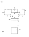
- Fig. 1 (a) illustrates an example of a mounting device used in the present invention in a schematic partial cross-sectional view
- Fig. 1 (b) illustrates an example of a pressing side of the thermocompression head in the mounting device in a schematic diagram
- Figs. 2 (a) and (b) illustrate a measurement relationship between a pressing surface of the thermocompression head and a top region of an electric component in schematic diagrams.
- a mounting device 1 includes a base 2 placing thereon a wiring board 10 having a wiring pattern (not shown) and a thermocompression head 3 applying pressure and heat to an electric component 20 serving as a target to be thermally compressed such as an IC chip.
- the base 2 is made of prescribed metal and includes a heater (not shown) for heating disposed inside thereof.
- the electric component 20 is in such a manner as to be disposed, through an adhesive agent 30, in a prescribed position on the wiring board 10 placed on the base 2.
- any one of an insulating adhesive agent and an anisotropic conductive adhesive agent can be used as the adhesive agent 30.
- the anisotropic conductive adhesive agent is preferable from a standpoint of connection reliability enhancement.
- a film form and a paste form can be used.
- thermocompression head 3 includes a head main body 5, for example, made of a metal material such as a stainless steel, and the head main body 5 includes a heater 6 for heating disposed inside thereof.
- the head main body 5 is made of the metal member in a box frame shape, for example, and includes a recess portion 5a that is disposed in a portion opposite to the base 2.
- a metal pressing member 5b (described later) is, for example, integrally provided in the head main body 5 by integral molding in a position (e.g., in a middle portion) corresponding to the electric component 20 of the recess portion 5a of the head main body 5.
- the elastic pressing-bonding member 7 is attached so that a pressing surface 50 of the metal pressing member 5b is exposed in a recessed state with respect to a surface 70 of the elastic pressing-bonding member 7 on the periphery of the metal pressing member 5b.
- the metal pressing member 5b for example, is formed in a quadrangular prism shape and has the pressing surface 50 of a rectangular plane shape in an end portion thereof.
- a size of the pressing surface 50 of the metal pressing member 5b is not particularly limited.
- the size of the pressing surface 50 is preferably arranged to be slightly smaller than a size of a surface of the electric component 20 to be pressed from a standpoint in which the heat and pressure is surely applied by the elastic pressure bonding member 7 in such a manner as not to generate a void with respect to a fillet portion of the adhesive agent 30 on the periphery of the electric component 20.
- a size (outside dimension) of the pressing surface 50 of the metal pressing member 5b is preferably arranged to be slightly smaller than a size (outside dimension) of a top region 21 of the electric component 20 as illustrated in Figs. 2 (a) and (b) .
- a height difference "H" between the pressing surface 50 of the metal pressing member 5b and the surface 70 of the elastic pressure bonding member 7 is preferably arranged to be greater than a thickness "h" of the electric component 20 as illustrated in Fig. 2 (a) from a standpoint in which the pressure is surely applied in such a manner as not to generate the void with respect to the fillet portion of the adhesive agent 30 on the periphery of the electric component 20 although the present invention is not particularly limited thereby.
- a portion on the periphery of the metal pressing member 5b of the elastic pressure bonding member 7 is preferably formed in a taper shape toward an outward of an opening 8 from a standpoint in which the pressing surface 50 of the metal pressing member 5b is smoothly in close contact with respect to the top region 21 of the electric component 20, and the pressure is surely applied in such a manner as not to generate the void with respect to the fillet portion of the adhesive agent 30 on the periphery although the present invention is not particularly limited thereby.
- a taper section 7a having a prescribed angle is formed in an opening wall surface portion of the elastic pressure bonding member 7, and the opening 8 on the pressing surface 50 of the elastic pressure bonding member 7 is preferably sized greater than the top region 21 of the electric component 20.
- An angle of the taper section 7a of the elastic pressure bonding member 7 can be arranged as needed according to the sizes of the pressing surface 50 of the metal pressing member 5b and the top region 21 of the electric component 20 and the height "H" of the surface 70 of the elastic pressure bonding member 7 with respect to the pressing surface 50 of the metal pressing member 5b.
- Figs. 3 (a) through (c) illustrate a mounting method according to the embodiment of the present invention in process diagrams
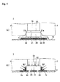
- Figs. 4 (a) and (b) illustrate essential portions of the mounting method in schematic diagrams.
- the adhesive agent 30 is provided on a mounting region of the wiring board 10 placed on the base 2, and the electric component 20 is disposed in a prescribed position on the adhesive agent 30 as illustrated in Fig. 3 (a) .
- the heater 6 disposed inside the head main body 5 is controlled, so that the metal pressing member 5b and the elastic pressure-bonging member 7 are heated to prescribed temperature, and the base 2 is heated to prescribed temperature.
- a protection film (not shown) is disposed on the electric component 20 and is thermally compressed in a tentative manner with a prescribed condition (positioning)
- the head main body 5 is moved downward as illustrated in Fig. 3 (b) , so that the heat and pressure is applied with respect to the electric component 20 for a prescribed time period as the thermocompression in a permanent manner.
- the taper section 7a of the elastic pressure bonding member 7 contacts an edge 21a of the top region 21 of the electric component 20, and such a guidance movement allows the electric component 20 to be smoothly in close contact with respect to the pressing surface 50 of the metal pressing member 5b.
- the fillet portion 30f of the adhesive agent 30 on the periphery of the electric component 20 is pressed toward a side of a side portion region 22 of the electric component 20 by a surface of the taper section 7a of the elastic pressure bonding member 7. Therefore, the electric component 20 is mounted on the wiring board 10 in a state that the fillet portion 30f of the adhesive agent 30 is adequately pressed.
- thermocompression bonding in a case of the thermocompression bonding, the heat and pressure is applied with respect to the top region 21 of the electric component 20 by the metal pressing member 5b being in close contact therewith while applying the heat and pressure with respect to the fillet portion 30f of the adhesive agent 30 on the periphery by the elastic pressure bonding member 7 made of the elastomer. Consequently, the electric component 20 is thermally compressed in a short time, and the thermocompression bonding can by performed with respect to the fillet portion 30f of the adhesive agent 30 on the periphery of the electric component 20 in such a manner not to generate the void, thereby allowing connection of the electric component 20 with high reliability by using the adhesive agent.
- one metal pressing member is provided to the head main body, and the thermocompression is performed with respect to one electric component in the above embodiment.
- the present invention is not limited thereto.
- a plurality of the metal pressing members may be provided to the head main body, and a plurality of electric components may be thermally compressed in a simultaneous manner.
- dispositions and shapes of the metal pressing member and the pressing surface of the thermocomprssion head used in the present invention may be modified as needed according to the electric component to be the target of the thermocompression bonding.
- the present invention may be applied to a variety of the electric components such as an IC chip and a capacitor.
Landscapes
- Engineering & Computer Science (AREA)
- Mechanical Engineering (AREA)
- Manufacturing & Machinery (AREA)
- Microelectronics & Electronic Packaging (AREA)
- Physics & Mathematics (AREA)
- Fluid Mechanics (AREA)
- Electric Connection Of Electric Components To Printed Circuits (AREA)
- Wire Bonding (AREA)
Abstract
Description
- The present invention relates to a technology for mounting a variety of electric components. More particularly, the present invention relates to a mounting method using a thermocompression head for mounting an electric component using an adhesive agent.
- Generally, in a case where passive components such as resistors and capacitors are mounted on a wiring board, solder serving as a connecting material is melted in a reflow furnace so as to mount the passive components.
- On the other hand, in a case where electric components such as IC chips are mounted on a wiring board, the electric components are packaged and mounted by solder, or the IC chips are directly placed on the wiring board and mounted by wire bonding or flip chip.
In a case where such electric components are mounted by the flip chip using a conductive adhesive agent and the like, a hard pressure bonding head made of metal and/or ceramic and the like is generally used to perform thermocompression bonding. - In recent years, however, a pressure bonding head made of a member having elasticity such as silicone rubber is also used to perform the thermocompression bonding.
In a case where such an elastic member is used as the pressure bonding head, there is an advantage that not only a plurality of electric components having different heights can be bonded with pressure, but also a variety of different electric components such as the resistors and the capacitors in addition to the IC chips can be collectively bonded with the pressure in a simultaneous manner (e.g., patent document 1). - However, in a case where the pressure bonding head made of the metal and/or ceramic is used, insufficient heat with respect to a fillet portion of the adhesive agent on the periphery of the electric component generates a void in the course of the thermocompression bonding, causing a problem of deteriorating connection reliability.
On the other hand, in a case where the pressure bonding head made of the elastic member described above is used, heat from a side of the pressure bonding head is not adequate, causing a problem of prolonging a time for mounting.
Patent Document 1: Japanese Patent Laid-Open Publication2005-32952 - The present invention is proposed in consideration of the aforementioned conventional situations. Moreover, the object of the present invention is intended to provide a mounting method of mounting an electric component on a wiring board in a short time with high connection reliability using a thermocompression head.
- To achieve the aforementioned objects, a method of mounting an electric component on a wiring board using a thermocompression head having an elastic pressure bonding member made of elastomer in a metal head main body made of heatable metal is provided. The method includes the steps of: disposing an adhesive agent in a mounting region on the wiring board; disposing the electric component in the mounting region; and thermally compressing the electric component on the wiring board using the thermocompression head. The thermally compressing step presses a top region of the electric component by a metal portion of the head main body while pressing the adhesive agent in a vicinity of a side portion region of the electric component by the elastic pressure bonding member.
According to the present invention, a periphery of a metal pressing portion of the elastic pressure bonding member is formed in a taper shape, and the adhesive agent in the vicinity of the side portion region of the electric component is pressed toward the side portion region by the taper portion. - According to the present invention, in a case of the thermocompression bonding, the heat and pressure is applied with respect to the top region of the electric component by the metal pressing member being in close contact therewith while applying the heat and pressure with respect to a fillet portion of the adhesive agent in the vicinity of the side portion region by the elastic pressure bonding member made of the elastomer. Consequently, the electric component is thermally compressed in a short time, and the thermocompression bonding can by performed with respect to the fillet portion of the adhesive agent on the periphery of the electric component in such a manner not to generate the void, thereby allowing connection of the electric component with high reliability by using the adhesive agent.
- According to the present invention, in a case where the thermocompression head formed in the taper shape in a portion on the periphery of the metal pressing member of the elastic pressure bonding member is used, and the adhesive agent in the vicinity of the side portion region of the electric component is pressed toward the side portion region by the taper portion, the taper portion of the elastic pressure bonding member contacts an edge portion of a surface of the electric component to be pressed in a case of the thermocompression bonding. Such a guidance movement allows the electric component to be smoothly in close contact with respect to a pressing surface of the metal pressing member, and the fillet portion of the adhesive agent on the periphery of the electric component is surely pressed by a surface of the taper portion of the elastic pressure bonding member, thereby reducing generation of a void.
- According to the present invention, not only an electric component is thermally compressed in a short time, but also a fillet portion of an adhesive agent on the periphery of the electric component is thermally compressed without generating a void, thereby allowing connection of the electric component with high reliability by using the adhesive agent.
-
-
Fig. 1 (a) is a schematic partial cross-sectional view illustrating an example of a mounting device used in the present invention, andFIG 1 (b) is a schematic diagram illustrating a pressing side of a thermocompression head in the mounting device; -
Figs. 2 (a) and (b) are schematic diagrams illustrating a measurement relationship between a pressing surface of the thermocompression head and a top region of an electric component; -
Figs. 3 (a) through (c) are process diagrams illustrating a mounting method according to the present invention; and -
Figs. 4 (a) and (b) are schematic diagrams illustrating essential portions of the mounting method. -
- 1:
- Mounting device
- 2:
- Base
- 3:
- Thermocompression head
- 5:
- Head main body
- 5a:
- Recess portion
- 5b:
- Metal pressing member
- 6:
- Heater
- 7:
- Elastic pressure bonding member
- 7a:
- Taper section
- 8:
- Opening
- 10:
- Wiring board
- 20:
- Electric component
- 21:
- Top region (surface to be pressed)
- 30:
- Adhesive agent
- 30f:
- Fillet portion
- 50:
- Pressing surface
- Hereinafter, a mounting method using a thermocompression head according to an embodiment of the present invention will be explained in detail with reference to the drawings.
-
Fig. 1 (a) illustrates an example of a mounting device used in the present invention in a schematic partial cross-sectional view, andFig. 1 (b) illustrates an example of a pressing side of the thermocompression head in the mounting device in a schematic diagram.
Figs. 2 (a) and (b) illustrate a measurement relationship between a pressing surface of the thermocompression head and a top region of an electric component in schematic diagrams. - As illustrated in
Figs. 1 (a) and (b) , a mountingdevice 1 according to the embodiment includes abase 2 placing thereon awiring board 10 having a wiring pattern (not shown) and athermocompression head 3 applying pressure and heat to anelectric component 20 serving as a target to be thermally compressed such as an IC chip. - Wherein, the
base 2 is made of prescribed metal and includes a heater (not shown) for heating disposed inside thereof. Theelectric component 20 is in such a manner as to be disposed, through anadhesive agent 30, in a prescribed position on thewiring board 10 placed on thebase 2. - In a case of the present invention, any one of an insulating adhesive agent and an anisotropic conductive adhesive agent can be used as the
adhesive agent 30.
Among such agents, the anisotropic conductive adhesive agent is preferable from a standpoint of connection reliability enhancement.
Regarding the anisotropic conductive adhesive agent, a film form and a paste form can be used. - On the other hand, the
thermocompression head 3 includes a headmain body 5, for example, made of a metal material such as a stainless steel, and the headmain body 5 includes aheater 6 for heating disposed inside thereof. - The head
main body 5 is made of the metal member in a box frame shape, for example, and includes arecess portion 5a that is disposed in a portion opposite to thebase 2.
Ametal pressing member 5b (described later) is, for example, integrally provided in the headmain body 5 by integral molding in a position (e.g., in a middle portion) corresponding to theelectric component 20 of therecess portion 5a of the headmain body 5. - Moreover, in the
recess portion 5a of the headmain body 5, an elastic pressing-bonding member 7 made of elastomer (silicone rubber and the like) in a plate shape, for example, is attached in such a manner as to be in close contact with the inside therecess portion 5a.
The elastic pressing-bonding member 7 is attached so that apressing surface 50 of themetal pressing member 5b is exposed in a recessed state with respect to asurface 70 of the elastic pressing-bonding member 7 on the periphery of themetal pressing member 5b.
Themetal pressing member 5b, for example, is formed in a quadrangular prism shape and has thepressing surface 50 of a rectangular plane shape in an end portion thereof. - With the present invention, a size of the
pressing surface 50 of themetal pressing member 5b is not particularly limited. However, the size of thepressing surface 50 is preferably arranged to be slightly smaller than a size of a surface of theelectric component 20 to be pressed from a standpoint in which the heat and pressure is surely applied by the elasticpressure bonding member 7 in such a manner as not to generate a void with respect to a fillet portion of theadhesive agent 30 on the periphery of theelectric component 20. - With the embodiment, for example, a size (outside dimension) of the
pressing surface 50 of themetal pressing member 5b is preferably arranged to be slightly smaller than a size (outside dimension) of atop region 21 of theelectric component 20 as illustrated inFigs. 2 (a) and (b) . - With the present invention, on the other hand, for example, a height difference "H" between the
pressing surface 50 of themetal pressing member 5b and thesurface 70 of the elasticpressure bonding member 7 is preferably arranged to be greater than a thickness "h" of theelectric component 20 as illustrated inFig. 2 (a) from a standpoint in which the pressure is surely applied in such a manner as not to generate the void with respect to the fillet portion of theadhesive agent 30 on the periphery of theelectric component 20 although the present invention is not particularly limited thereby. - Moreover, with the present invention, a portion on the periphery of the
metal pressing member 5b of the elasticpressure bonding member 7 is preferably formed in a taper shape toward an outward of an opening 8 from a standpoint in which thepressing surface 50 of themetal pressing member 5b is smoothly in close contact with respect to thetop region 21 of theelectric component 20, and the pressure is surely applied in such a manner as not to generate the void with respect to the fillet portion of theadhesive agent 30 on the periphery although the present invention is not particularly limited thereby.
In other words, ataper section 7a having a prescribed angle is formed in an opening wall surface portion of the elasticpressure bonding member 7, and the opening 8 on thepressing surface 50 of the elasticpressure bonding member 7 is preferably sized greater than thetop region 21 of theelectric component 20. - An angle of the
taper section 7a of the elasticpressure bonding member 7 can be arranged as needed according to the sizes of thepressing surface 50 of themetal pressing member 5b and thetop region 21 of theelectric component 20 and the height "H" of thesurface 70 of the elasticpressure bonding member 7 with respect to thepressing surface 50 of themetal pressing member 5b. -
Figs. 3 (a) through (c) illustrate a mounting method according to the embodiment of the present invention in process diagrams, andFigs. 4 (a) and (b) illustrate essential portions of the mounting method in schematic diagrams.
In the embodiment, theadhesive agent 30 is provided on a mounting region of thewiring board 10 placed on thebase 2, and theelectric component 20 is disposed in a prescribed position on theadhesive agent 30 as illustrated inFig. 3 (a) . - Herein, the
heater 6 disposed inside the headmain body 5 is controlled, so that themetal pressing member 5b and the elastic pressure-bongingmember 7 are heated to prescribed temperature, and thebase 2 is heated to prescribed temperature.
After a protection film (not shown) is disposed on theelectric component 20 and is thermally compressed in a tentative manner with a prescribed condition (positioning), the headmain body 5 is moved downward as illustrated inFig. 3 (b) , so that the heat and pressure is applied with respect to theelectric component 20 for a prescribed time period as the thermocompression in a permanent manner. - In a case where the head
main body 5 is moved downward, as illustrated inFig. 4 (a) , thetaper section 7a of the elasticpressure bonding member 7 contacts anedge 21a of thetop region 21 of theelectric component 20, and such a guidance movement allows theelectric component 20 to be smoothly in close contact with respect to thepressing surface 50 of themetal pressing member 5b.
Moreover, as illustrated inFig. 4(b) , thefillet portion 30f of theadhesive agent 30 on the periphery of theelectric component 20 is pressed toward a side of aside portion region 22 of theelectric component 20 by a surface of thetaper section 7a of the elasticpressure bonding member 7.
Therefore, theelectric component 20 is mounted on thewiring board 10 in a state that thefillet portion 30f of theadhesive agent 30 is adequately pressed. - According to the embodiment described above, in a case of the thermocompression bonding, the heat and pressure is applied with respect to the
top region 21 of theelectric component 20 by themetal pressing member 5b being in close contact therewith while applying the heat and pressure with respect to thefillet portion 30f of theadhesive agent 30 on the periphery by the elasticpressure bonding member 7 made of the elastomer. Consequently, theelectric component 20 is thermally compressed in a short time, and the thermocompression bonding can by performed with respect to thefillet portion 30f of theadhesive agent 30 on the periphery of theelectric component 20 in such a manner not to generate the void, thereby allowing connection of theelectric component 20 with high reliability by using the adhesive agent. - The present invention is not limited to the embodiment described above, and numerous additional modifications and variation of the present invention are possible.
For example, one metal pressing member is provided to the head main body, and the thermocompression is performed with respect to one electric component in the above embodiment. However, the present invention is not limited thereto. A plurality of the metal pressing members may be provided to the head main body, and a plurality of electric components may be thermally compressed in a simultaneous manner. - Moreover, dispositions and shapes of the metal pressing member and the pressing surface of the thermocomprssion head used in the present invention may be modified as needed according to the electric component to be the target of the thermocompression bonding.
Moreover, the present invention may be applied to a variety of the electric components such as an IC chip and a capacitor.
Claims (2)
- A method of mounting an electric component on a wiring board using a thermocompression head having an elastic pressure bonding member made of elastomer in a metal head main body made of heatable metal, the method comprising the steps of:disposing an adhesive agent in a mounting region on the wiring board;disposing the electric component in the mounting region; andthermally compressing the electric component on the wiring board using the thermocompression head,wherein the thermally compressing step using the thermocompression head presses a top region of the electric component by a metal portion of the head main body while pressing the adhesive agent in a vicinity of a side portion region of the electric component by the elastic pressure bonding member.
- A method of mounting using the thermocompression head according to claim 1, wherein a periphery of the metal pressing portion of the elastic pressure bonding member is formed in a taper shape, and the adhesive agent in the vicinity of the side portion region of the electric component is pressed toward the side portion region by the taper portion.
Applications Claiming Priority (2)
| Application Number | Priority Date | Filing Date | Title |
|---|---|---|---|
| JP2006197275A JP4979288B2 (en) | 2006-07-19 | 2006-07-19 | Mounting method using thermocompression bonding head |
| PCT/JP2007/064184 WO2008010516A1 (en) | 2006-07-19 | 2007-07-18 | Mounting method using thermocompression head |
Publications (3)
| Publication Number | Publication Date |
|---|---|
| EP2043142A1 true EP2043142A1 (en) | 2009-04-01 |
| EP2043142A4 EP2043142A4 (en) | 2009-12-02 |
| EP2043142B1 EP2043142B1 (en) | 2011-10-19 |
Family
ID=38956848
Family Applications (1)
| Application Number | Title | Priority Date | Filing Date |
|---|---|---|---|
| EP07790938A Not-in-force EP2043142B1 (en) | 2006-07-19 | 2007-07-18 | Mounting method using thermocompression head |
Country Status (7)
| Country | Link |
|---|---|
| US (1) | US8114243B2 (en) |
| EP (1) | EP2043142B1 (en) |
| JP (1) | JP4979288B2 (en) |
| KR (1) | KR101034166B1 (en) |
| CN (1) | CN101490831B (en) |
| TW (1) | TWI411053B (en) |
| WO (1) | WO2008010516A1 (en) |
Families Citing this family (14)
| Publication number | Priority date | Publication date | Assignee | Title |
|---|---|---|---|---|
| WO2009001564A1 (en) | 2007-06-28 | 2008-12-31 | Panasonic Corporation | Semiconductor element mounting structure, method for manufacturing the semiconductor element mounting structure, semiconductor element mounting method and pressurizing tool |
| JP2011009357A (en) * | 2009-06-24 | 2011-01-13 | Fujitsu Ltd | Mounting device |
| JP5608545B2 (en) * | 2010-12-24 | 2014-10-15 | デクセリアルズ株式会社 | Thermocompression bonding head, mounting apparatus and mounting method |
| JP2013191669A (en) * | 2012-03-13 | 2013-09-26 | Shinkawa Ltd | Electronic component mounting tool |
| US9093549B2 (en) * | 2013-07-02 | 2015-07-28 | Kulicke And Soffa Industries, Inc. | Bond heads for thermocompression bonders, thermocompression bonders, and methods of operating the same |
| US20150262966A1 (en) * | 2014-03-15 | 2015-09-17 | Dong Guan Cowell Optic Electronics Limited | Method and apparatus for bonding a semiconductor device or component to a substrate |
| GB2525605B (en) * | 2014-04-28 | 2018-10-24 | Flexenable Ltd | Method of bonding flexible printed circuits |
| DE102014114093B4 (en) | 2014-09-29 | 2017-03-23 | Danfoss Silicon Power Gmbh | Method for low-temperature pressure sintering |
| DE102014114097B4 (en) | 2014-09-29 | 2017-06-01 | Danfoss Silicon Power Gmbh | Sintering tool and method for sintering an electronic assembly |
| DE102014114096A1 (en) | 2014-09-29 | 2016-03-31 | Danfoss Silicon Power Gmbh | Sintering tool for the lower punch of a sintering device |
| DE102014114095B4 (en) * | 2014-09-29 | 2017-03-23 | Danfoss Silicon Power Gmbh | sintering apparatus |
| US11024595B2 (en) * | 2017-06-16 | 2021-06-01 | Micron Technology, Inc. | Thermocompression bond tips and related apparatus and methods |
| CN111526673A (en) * | 2019-02-01 | 2020-08-11 | 泰拉丁公司 | maintain the shape of the board |
| CN114597138A (en) * | 2020-12-03 | 2022-06-07 | 群创光电股份有限公司 | Manufacturing method of semiconductor package |
Family Cites Families (13)
| Publication number | Priority date | Publication date | Assignee | Title |
|---|---|---|---|---|
| US4963208A (en) * | 1987-10-06 | 1990-10-16 | Muncy Charles W | System for applying decorative devices to garments and the like |
| JPH0418840A (en) * | 1990-05-11 | 1992-01-23 | Fujitsu Ltd | Memo reproduction control system |
| JPH04188840A (en) * | 1990-11-22 | 1992-07-07 | Toshiba Corp | Die bonding method |
| JP3017485B2 (en) * | 1998-01-23 | 2000-03-06 | アピックヤマダ株式会社 | Resin sealing method and resin sealing device for semiconductor device |
| JP2001160564A (en) * | 1999-12-03 | 2001-06-12 | Apic Yamada Corp | Resin sealing apparatus |
| JP4718734B2 (en) * | 2001-09-12 | 2011-07-06 | 日機装株式会社 | Circuit element mounting method |
| JP4288026B2 (en) * | 2001-09-28 | 2009-07-01 | パナソニック株式会社 | Mounting tool and IC chip mounting method |
| DE10201430A1 (en) | 2002-01-16 | 2003-08-14 | Siemens Ag | Procedure for reversing the direction of rotation in two-stroke engines |
| JP3921459B2 (en) * | 2003-07-11 | 2007-05-30 | ソニーケミカル&インフォメーションデバイス株式会社 | Mounting method and mounting apparatus for electrical parts |
| JP2005032958A (en) | 2003-07-11 | 2005-02-03 | Nikon Corp | Method for adjusting illumination condition of charged particle beam apparatus and exposure method |
| TWI241720B (en) * | 2004-01-16 | 2005-10-11 | Super Nova Optoelectronics Cor | Replaceable light emitting diode packaging structure |
| EP1845556A4 (en) * | 2005-02-02 | 2010-02-10 | Sony Chem & Inf Device Corp | APPARATUS FOR MOUNTING ELECTRICAL COMPONENTS |
| JP2007324413A (en) * | 2006-06-01 | 2007-12-13 | Sony Chemical & Information Device Corp | Thermocompression bonding head and mounting apparatus using the same |
-
2006
- 2006-07-19 JP JP2006197275A patent/JP4979288B2/en not_active Expired - Fee Related
-
2007
- 2007-07-18 CN CN2007800273967A patent/CN101490831B/en not_active Expired - Fee Related
- 2007-07-18 US US12/374,240 patent/US8114243B2/en not_active Expired - Fee Related
- 2007-07-18 EP EP07790938A patent/EP2043142B1/en not_active Not-in-force
- 2007-07-18 KR KR1020097000771A patent/KR101034166B1/en not_active Expired - Fee Related
- 2007-07-18 WO PCT/JP2007/064184 patent/WO2008010516A1/en not_active Ceased
- 2007-07-19 TW TW096126279A patent/TWI411053B/en not_active IP Right Cessation
Also Published As
| Publication number | Publication date |
|---|---|
| TW200829106A (en) | 2008-07-01 |
| TWI411053B (en) | 2013-10-01 |
| HK1133738A1 (en) | 2010-04-01 |
| US20090261149A1 (en) | 2009-10-22 |
| CN101490831B (en) | 2011-09-28 |
| KR101034166B1 (en) | 2011-05-12 |
| EP2043142A4 (en) | 2009-12-02 |
| JP2008028039A (en) | 2008-02-07 |
| KR20090031902A (en) | 2009-03-30 |
| CN101490831A (en) | 2009-07-22 |
| US8114243B2 (en) | 2012-02-14 |
| WO2008010516A1 (en) | 2008-01-24 |
| EP2043142B1 (en) | 2011-10-19 |
| JP4979288B2 (en) | 2012-07-18 |
Similar Documents
| Publication | Publication Date | Title |
|---|---|---|
| EP2043142B1 (en) | Mounting method using thermocompression head | |
| JP4841431B2 (en) | Electrical component mounting equipment | |
| JPH11191569A (en) | Flip chip mounting method and semiconductor device | |
| JP2001313314A (en) | Semiconductor device using bump, method of manufacturing the same, and method of forming bump | |
| JP5854140B2 (en) | Semiconductor device and manufacturing method of semiconductor device | |
| US20170141022A1 (en) | Semiconductor device and method of manufacturing semiconductor device | |
| EP2023385A1 (en) | Thermocompression bonding head and mounting device using the same | |
| KR20160127807A (en) | Crimp head, and mounting device and mounting method using same | |
| JP2010092918A (en) | Connection structure and connection method between plate electrode and block electrode | |
| JP4334335B2 (en) | Method for manufacturing hybrid integrated circuit device | |
| JP2005191147A (en) | Method for manufacturing hybrid integrated circuit device | |
| JP2013229358A (en) | Semiconductor device and method of manufacturing the same | |
| JP2001267366A (en) | Semiconductor mounting method and printed circuit board | |
| US20070202633A1 (en) | Semiconductor package and method for fabricating the same | |
| JP5451053B2 (en) | Flip chip mounting method and flip chip mounting apparatus | |
| HK1133738B (en) | Mounting method using thermocompression head | |
| JPH11204575A (en) | Circuit board, mounting device and mounting method | |
| JP3586162B2 (en) | Method for forming package for electronic component | |
| JP2002299810A (en) | Electronic component mounting method | |
| JP2003037225A (en) | Thermal conductive sheet for cooling electronic components and cooling structure for electronic components | |
| JP2003243447A (en) | Semiconductor element mounting method | |
| JP2007059811A (en) | Electronics | |
| HK1116920B (en) | Electric component mounting apparatus | |
| JP2000058719A (en) | Semiconductor device and method of manufacturing semiconductor device | |
| JP2006294730A (en) | Semiconductor device manufacturing method and semiconductor device manufacturing apparatus |
Legal Events
| Date | Code | Title | Description |
|---|---|---|---|
| PUAI | Public reference made under article 153(3) epc to a published international application that has entered the european phase |
Free format text: ORIGINAL CODE: 0009012 |
|
| 17P | Request for examination filed |
Effective date: 20090112 |
|
| AK | Designated contracting states |
Kind code of ref document: A1 Designated state(s): AT BE BG CH CY CZ DE DK EE ES FI FR GB GR HU IE IS IT LI LT LU LV MC MT NL PL PT RO SE SI SK TR |
|
| AX | Request for extension of the european patent |
Extension state: AL BA HR MK RS |
|
| DAX | Request for extension of the european patent (deleted) | ||
| RBV | Designated contracting states (corrected) |
Designated state(s): DE FR GB IT NL |
|
| A4 | Supplementary search report drawn up and despatched |
Effective date: 20091104 |
|
| 17Q | First examination report despatched |
Effective date: 20100204 |
|
| GRAP | Despatch of communication of intention to grant a patent |
Free format text: ORIGINAL CODE: EPIDOSNIGR1 |
|
| RIC1 | Information provided on ipc code assigned before grant |
Ipc: H05K 3/32 20060101ALI20110418BHEP Ipc: H01L 21/60 20060101AFI20110418BHEP Ipc: H01L 21/603 20060101ALI20110418BHEP |
|
| GRAS | Grant fee paid |
Free format text: ORIGINAL CODE: EPIDOSNIGR3 |
|
| GRAA | (expected) grant |
Free format text: ORIGINAL CODE: 0009210 |
|
| AK | Designated contracting states |
Kind code of ref document: B1 Designated state(s): DE FR GB IT NL |
|
| REG | Reference to a national code |
Ref country code: GB Ref legal event code: FG4D |
|
| REG | Reference to a national code |
Ref country code: DE Ref legal event code: R096 Ref document number: 602007018088 Country of ref document: DE Effective date: 20111222 |
|
| REG | Reference to a national code |
Ref country code: NL Ref legal event code: T3 |
|
| PLBE | No opposition filed within time limit |
Free format text: ORIGINAL CODE: 0009261 |
|
| STAA | Information on the status of an ep patent application or granted ep patent |
Free format text: STATUS: NO OPPOSITION FILED WITHIN TIME LIMIT |
|
| PG25 | Lapsed in a contracting state [announced via postgrant information from national office to epo] |
Ref country code: IT Free format text: LAPSE BECAUSE OF FAILURE TO SUBMIT A TRANSLATION OF THE DESCRIPTION OR TO PAY THE FEE WITHIN THE PRESCRIBED TIME-LIMIT Effective date: 20111019 |
|
| 26N | No opposition filed |
Effective date: 20120720 |
|
| REG | Reference to a national code |
Ref country code: DE Ref legal event code: R097 Ref document number: 602007018088 Country of ref document: DE Effective date: 20120720 |
|
| REG | Reference to a national code |
Ref country code: FR Ref legal event code: PLFP Year of fee payment: 10 |
|
| PGFP | Annual fee paid to national office [announced via postgrant information from national office to epo] |
Ref country code: FR Payment date: 20160613 Year of fee payment: 10 Ref country code: NL Payment date: 20160610 Year of fee payment: 10 |
|
| PGFP | Annual fee paid to national office [announced via postgrant information from national office to epo] |
Ref country code: DE Payment date: 20160712 Year of fee payment: 10 Ref country code: GB Payment date: 20160713 Year of fee payment: 10 |
|
| REG | Reference to a national code |
Ref country code: DE Ref legal event code: R119 Ref document number: 602007018088 Country of ref document: DE |
|
| REG | Reference to a national code |
Ref country code: NL Ref legal event code: MM Effective date: 20170801 |
|
| GBPC | Gb: european patent ceased through non-payment of renewal fee |
Effective date: 20170718 |
|
| REG | Reference to a national code |
Ref country code: FR Ref legal event code: ST Effective date: 20180330 |
|
| PG25 | Lapsed in a contracting state [announced via postgrant information from national office to epo] |
Ref country code: GB Free format text: LAPSE BECAUSE OF NON-PAYMENT OF DUE FEES Effective date: 20170718 Ref country code: NL Free format text: LAPSE BECAUSE OF NON-PAYMENT OF DUE FEES Effective date: 20170801 Ref country code: DE Free format text: LAPSE BECAUSE OF NON-PAYMENT OF DUE FEES Effective date: 20180201 |
|
| PG25 | Lapsed in a contracting state [announced via postgrant information from national office to epo] |
Ref country code: FR Free format text: LAPSE BECAUSE OF NON-PAYMENT OF DUE FEES Effective date: 20170731 |