EP2042467A1 - Procédé de fabrication d'un composant microfluidique comportant au moins un microcanal rempli de nanostructures - Google Patents
Procédé de fabrication d'un composant microfluidique comportant au moins un microcanal rempli de nanostructures Download PDFInfo
- Publication number
- EP2042467A1 EP2042467A1 EP08354060A EP08354060A EP2042467A1 EP 2042467 A1 EP2042467 A1 EP 2042467A1 EP 08354060 A EP08354060 A EP 08354060A EP 08354060 A EP08354060 A EP 08354060A EP 2042467 A1 EP2042467 A1 EP 2042467A1
- Authority
- EP
- European Patent Office
- Prior art keywords
- microchannel
- cover
- metal catalyst
- nanostructures
- substrate
- Prior art date
- Legal status (The legal status is an assumption and is not a legal conclusion. Google has not performed a legal analysis and makes no representation as to the accuracy of the status listed.)
- Granted
Links
- 239000002086 nanomaterial Substances 0.000 title claims abstract description 38
- 238000004519 manufacturing process Methods 0.000 title claims description 16
- 229910052751 metal Inorganic materials 0.000 claims abstract description 47
- 239000002184 metal Substances 0.000 claims abstract description 47
- 239000003054 catalyst Substances 0.000 claims abstract description 46
- 239000000758 substrate Substances 0.000 claims abstract description 39
- 238000000034 method Methods 0.000 claims abstract description 31
- 230000015572 biosynthetic process Effects 0.000 claims abstract description 21
- VYPSYNLAJGMNEJ-UHFFFAOYSA-N Silicium dioxide Chemical compound O=[Si]=O VYPSYNLAJGMNEJ-UHFFFAOYSA-N 0.000 claims abstract description 15
- 229910052710 silicon Inorganic materials 0.000 claims abstract description 13
- 239000010703 silicon Substances 0.000 claims abstract description 13
- XEEYBQQBJWHFJM-UHFFFAOYSA-N Iron Chemical compound [Fe] XEEYBQQBJWHFJM-UHFFFAOYSA-N 0.000 claims abstract description 12
- 239000000463 material Substances 0.000 claims abstract description 12
- 239000011521 glass Substances 0.000 claims abstract description 9
- PXHVJJICTQNCMI-UHFFFAOYSA-N Nickel Chemical compound [Ni] PXHVJJICTQNCMI-UHFFFAOYSA-N 0.000 claims abstract description 8
- 230000005496 eutectics Effects 0.000 claims abstract description 8
- 150000001875 compounds Chemical class 0.000 claims abstract description 7
- 238000011049 filling Methods 0.000 claims abstract description 7
- 229910052742 iron Inorganic materials 0.000 claims abstract description 6
- 229910052759 nickel Inorganic materials 0.000 claims abstract description 4
- 229910017052 cobalt Inorganic materials 0.000 claims abstract description 3
- 239000010941 cobalt Substances 0.000 claims abstract description 3
- GUTLYIVDDKVIGB-UHFFFAOYSA-N cobalt atom Chemical compound [Co] GUTLYIVDDKVIGB-UHFFFAOYSA-N 0.000 claims abstract description 3
- PCHJSUWPFVWCPO-UHFFFAOYSA-N gold Chemical compound [Au] PCHJSUWPFVWCPO-UHFFFAOYSA-N 0.000 claims abstract description 3
- 229910052737 gold Inorganic materials 0.000 claims abstract description 3
- 239000010931 gold Substances 0.000 claims abstract description 3
- 238000007789 sealing Methods 0.000 claims description 19
- 238000011065 in-situ storage Methods 0.000 claims description 13
- 238000010438 heat treatment Methods 0.000 claims description 5
- 229910052814 silicon oxide Inorganic materials 0.000 claims description 5
- 239000003863 metallic catalyst Substances 0.000 claims description 2
- 238000009434 installation Methods 0.000 claims 1
- 230000001681 protective effect Effects 0.000 abstract description 5
- 239000000377 silicon dioxide Substances 0.000 abstract description 4
- 235000012239 silicon dioxide Nutrition 0.000 abstract 1
- 238000007669 thermal treatment Methods 0.000 abstract 1
- 239000002071 nanotube Substances 0.000 description 17
- OKTJSMMVPCPJKN-UHFFFAOYSA-N Carbon Chemical compound [C] OKTJSMMVPCPJKN-UHFFFAOYSA-N 0.000 description 16
- XUIMIQQOPSSXEZ-UHFFFAOYSA-N Silicon Chemical compound [Si] XUIMIQQOPSSXEZ-UHFFFAOYSA-N 0.000 description 13
- 239000002041 carbon nanotube Substances 0.000 description 13
- 229910021393 carbon nanotube Inorganic materials 0.000 description 13
- 230000005526 G1 to G0 transition Effects 0.000 description 10
- 238000000151 deposition Methods 0.000 description 10
- 235000012431 wafers Nutrition 0.000 description 10
- 230000008021 deposition Effects 0.000 description 7
- 238000005530 etching Methods 0.000 description 6
- 239000002109 single walled nanotube Substances 0.000 description 6
- 238000004458 analytical method Methods 0.000 description 5
- 238000005229 chemical vapour deposition Methods 0.000 description 5
- 238000004587 chromatography analysis Methods 0.000 description 5
- 102000004190 Enzymes Human genes 0.000 description 4
- 108090000790 Enzymes Proteins 0.000 description 4
- 238000011161 development Methods 0.000 description 4
- 230000018109 developmental process Effects 0.000 description 4
- 239000012530 fluid Substances 0.000 description 4
- 238000000926 separation method Methods 0.000 description 4
- 239000000126 substance Substances 0.000 description 4
- 238000000708 deep reactive-ion etching Methods 0.000 description 3
- 238000001514 detection method Methods 0.000 description 3
- 238000004817 gas chromatography Methods 0.000 description 3
- 239000002048 multi walled nanotube Substances 0.000 description 3
- RUFLMLWJRZAWLJ-UHFFFAOYSA-N nickel silicide Chemical compound [Ni]=[Si]=[Ni] RUFLMLWJRZAWLJ-UHFFFAOYSA-N 0.000 description 3
- 229910021334 nickel silicide Inorganic materials 0.000 description 3
- BASFCYQUMIYNBI-UHFFFAOYSA-N platinum Chemical compound [Pt] BASFCYQUMIYNBI-UHFFFAOYSA-N 0.000 description 3
- 239000000243 solution Substances 0.000 description 3
- 229910001220 stainless steel Inorganic materials 0.000 description 3
- 239000010935 stainless steel Substances 0.000 description 3
- 238000003786 synthesis reaction Methods 0.000 description 3
- 239000002253 acid Substances 0.000 description 2
- 238000013459 approach Methods 0.000 description 2
- 230000003197 catalytic effect Effects 0.000 description 2
- 230000029087 digestion Effects 0.000 description 2
- 239000005350 fused silica glass Substances 0.000 description 2
- 238000002347 injection Methods 0.000 description 2
- 239000007924 injection Substances 0.000 description 2
- 238000004811 liquid chromatography Methods 0.000 description 2
- 238000007254 oxidation reaction Methods 0.000 description 2
- 239000012071 phase Substances 0.000 description 2
- 238000000206 photolithography Methods 0.000 description 2
- 239000011347 resin Substances 0.000 description 2
- 229920005989 resin Polymers 0.000 description 2
- GHYOCDFICYLMRF-UTIIJYGPSA-N (2S,3R)-N-[(2S)-3-(cyclopenten-1-yl)-1-[(2R)-2-methyloxiran-2-yl]-1-oxopropan-2-yl]-3-hydroxy-3-(4-methoxyphenyl)-2-[[(2S)-2-[(2-morpholin-4-ylacetyl)amino]propanoyl]amino]propanamide Chemical compound C1(=CCCC1)C[C@@H](C(=O)[C@@]1(OC1)C)NC([C@H]([C@@H](C1=CC=C(C=C1)OC)O)NC([C@H](C)NC(CN1CCOCC1)=O)=O)=O GHYOCDFICYLMRF-UTIIJYGPSA-N 0.000 description 1
- 241001415961 Gaviidae Species 0.000 description 1
- UFHFLCQGNIYNRP-UHFFFAOYSA-N Hydrogen Chemical compound [H][H] UFHFLCQGNIYNRP-UHFFFAOYSA-N 0.000 description 1
- ZOKXTWBITQBERF-UHFFFAOYSA-N Molybdenum Chemical compound [Mo] ZOKXTWBITQBERF-UHFFFAOYSA-N 0.000 description 1
- 229910008045 Si-Si Inorganic materials 0.000 description 1
- 229910006411 Si—Si Inorganic materials 0.000 description 1
- 241001080024 Telles Species 0.000 description 1
- 102000004142 Trypsin Human genes 0.000 description 1
- 108090000631 Trypsin Proteins 0.000 description 1
- 240000008042 Zea mays Species 0.000 description 1
- HSFWRNGVRCDJHI-UHFFFAOYSA-N alpha-acetylene Natural products C#C HSFWRNGVRCDJHI-UHFFFAOYSA-N 0.000 description 1
- 229910052782 aluminium Inorganic materials 0.000 description 1
- XAGFODPZIPBFFR-UHFFFAOYSA-N aluminium Chemical compound [Al] XAGFODPZIPBFFR-UHFFFAOYSA-N 0.000 description 1
- 150000001448 anilines Chemical class 0.000 description 1
- QVGXLLKOCUKJST-UHFFFAOYSA-N atomic oxygen Chemical compound [O] QVGXLLKOCUKJST-UHFFFAOYSA-N 0.000 description 1
- 239000011324 bead Substances 0.000 description 1
- 238000002045 capillary electrochromatography Methods 0.000 description 1
- 229910052799 carbon Inorganic materials 0.000 description 1
- 239000002134 carbon nanofiber Substances 0.000 description 1
- 238000003421 catalytic decomposition reaction Methods 0.000 description 1
- 238000006243 chemical reaction Methods 0.000 description 1
- 238000004140 cleaning Methods 0.000 description 1
- QGUAJWGNOXCYJF-UHFFFAOYSA-N cobalt dinitrate hexahydrate Chemical compound O.O.O.O.O.O.[Co+2].[O-][N+]([O-])=O.[O-][N+]([O-])=O QGUAJWGNOXCYJF-UHFFFAOYSA-N 0.000 description 1
- 229940125797 compound 12 Drugs 0.000 description 1
- 239000000470 constituent Substances 0.000 description 1
- 238000011109 contamination Methods 0.000 description 1
- 238000005520 cutting process Methods 0.000 description 1
- 230000003247 decreasing effect Effects 0.000 description 1
- 238000009792 diffusion process Methods 0.000 description 1
- 230000009977 dual effect Effects 0.000 description 1
- 125000002534 ethynyl group Chemical group [H]C#C* 0.000 description 1
- 238000001704 evaporation Methods 0.000 description 1
- 230000008020 evaporation Effects 0.000 description 1
- 238000001914 filtration Methods 0.000 description 1
- 239000007789 gas Substances 0.000 description 1
- 238000004128 high performance liquid chromatography Methods 0.000 description 1
- 239000001257 hydrogen Substances 0.000 description 1
- 229910052739 hydrogen Inorganic materials 0.000 description 1
- 239000012535 impurity Substances 0.000 description 1
- 230000010354 integration Effects 0.000 description 1
- 230000001678 irradiating effect Effects 0.000 description 1
- 238000002032 lab-on-a-chip Methods 0.000 description 1
- VNWKTOKETHGBQD-UHFFFAOYSA-N methane Chemical class C VNWKTOKETHGBQD-UHFFFAOYSA-N 0.000 description 1
- 238000004377 microelectronic Methods 0.000 description 1
- 239000000203 mixture Substances 0.000 description 1
- 229910052750 molybdenum Inorganic materials 0.000 description 1
- 239000011733 molybdenum Substances 0.000 description 1
- TXCOQXKFOPSCPZ-UHFFFAOYSA-J molybdenum(4+);tetraacetate Chemical compound [Mo+4].CC([O-])=O.CC([O-])=O.CC([O-])=O.CC([O-])=O TXCOQXKFOPSCPZ-UHFFFAOYSA-J 0.000 description 1
- 238000002414 normal-phase solid-phase extraction Methods 0.000 description 1
- 230000003287 optical effect Effects 0.000 description 1
- 230000003647 oxidation Effects 0.000 description 1
- 230000001590 oxidative effect Effects 0.000 description 1
- 239000001301 oxygen Substances 0.000 description 1
- 229910052760 oxygen Inorganic materials 0.000 description 1
- 238000012856 packing Methods 0.000 description 1
- 238000005289 physical deposition Methods 0.000 description 1
- 229910052697 platinum Inorganic materials 0.000 description 1
- 239000000843 powder Substances 0.000 description 1
- 239000002243 precursor Substances 0.000 description 1
- 238000002203 pretreatment Methods 0.000 description 1
- 108090000623 proteins and genes Proteins 0.000 description 1
- 102000004169 proteins and genes Human genes 0.000 description 1
- 230000005855 radiation Effects 0.000 description 1
- 230000035945 sensitivity Effects 0.000 description 1
- 238000005507 spraying Methods 0.000 description 1
- 238000011282 treatment Methods 0.000 description 1
- 239000012588 trypsin Substances 0.000 description 1
- 239000012808 vapor phase Substances 0.000 description 1
Images

Classifications
-
- B—PERFORMING OPERATIONS; TRANSPORTING
- B81—MICROSTRUCTURAL TECHNOLOGY
- B81C—PROCESSES OR APPARATUS SPECIALLY ADAPTED FOR THE MANUFACTURE OR TREATMENT OF MICROSTRUCTURAL DEVICES OR SYSTEMS
- B81C1/00—Manufacture or treatment of devices or systems in or on a substrate
- B81C1/00015—Manufacture or treatment of devices or systems in or on a substrate for manufacturing microsystems
- B81C1/00206—Processes for functionalising a surface, e.g. provide the surface with specific mechanical, chemical or biological properties
-
- B—PERFORMING OPERATIONS; TRANSPORTING
- B01—PHYSICAL OR CHEMICAL PROCESSES OR APPARATUS IN GENERAL
- B01J—CHEMICAL OR PHYSICAL PROCESSES, e.g. CATALYSIS OR COLLOID CHEMISTRY; THEIR RELEVANT APPARATUS
- B01J19/00—Chemical, physical or physico-chemical processes in general; Their relevant apparatus
- B01J19/0093—Microreactors, e.g. miniaturised or microfabricated reactors
-
- B—PERFORMING OPERATIONS; TRANSPORTING
- B01—PHYSICAL OR CHEMICAL PROCESSES OR APPARATUS IN GENERAL
- B01L—CHEMICAL OR PHYSICAL LABORATORY APPARATUS FOR GENERAL USE
- B01L3/00—Containers or dishes for laboratory use, e.g. laboratory glassware; Droppers
- B01L3/50—Containers for the purpose of retaining a material to be analysed, e.g. test tubes
- B01L3/502—Containers for the purpose of retaining a material to be analysed, e.g. test tubes with fluid transport, e.g. in multi-compartment structures
- B01L3/5027—Containers for the purpose of retaining a material to be analysed, e.g. test tubes with fluid transport, e.g. in multi-compartment structures by integrated microfluidic structures, i.e. dimensions of channels and chambers are such that surface tension forces are important, e.g. lab-on-a-chip
- B01L3/502707—Containers for the purpose of retaining a material to be analysed, e.g. test tubes with fluid transport, e.g. in multi-compartment structures by integrated microfluidic structures, i.e. dimensions of channels and chambers are such that surface tension forces are important, e.g. lab-on-a-chip characterised by the manufacture of the container or its components
-
- B—PERFORMING OPERATIONS; TRANSPORTING
- B01—PHYSICAL OR CHEMICAL PROCESSES OR APPARATUS IN GENERAL
- B01L—CHEMICAL OR PHYSICAL LABORATORY APPARATUS FOR GENERAL USE
- B01L3/00—Containers or dishes for laboratory use, e.g. laboratory glassware; Droppers
- B01L3/50—Containers for the purpose of retaining a material to be analysed, e.g. test tubes
- B01L3/502—Containers for the purpose of retaining a material to be analysed, e.g. test tubes with fluid transport, e.g. in multi-compartment structures
- B01L3/5027—Containers for the purpose of retaining a material to be analysed, e.g. test tubes with fluid transport, e.g. in multi-compartment structures by integrated microfluidic structures, i.e. dimensions of channels and chambers are such that surface tension forces are important, e.g. lab-on-a-chip
- B01L3/502753—Containers for the purpose of retaining a material to be analysed, e.g. test tubes with fluid transport, e.g. in multi-compartment structures by integrated microfluidic structures, i.e. dimensions of channels and chambers are such that surface tension forces are important, e.g. lab-on-a-chip characterised by bulk separation arrangements on lab-on-a-chip devices, e.g. for filtration or centrifugation
-
- B—PERFORMING OPERATIONS; TRANSPORTING
- B01—PHYSICAL OR CHEMICAL PROCESSES OR APPARATUS IN GENERAL
- B01J—CHEMICAL OR PHYSICAL PROCESSES, e.g. CATALYSIS OR COLLOID CHEMISTRY; THEIR RELEVANT APPARATUS
- B01J2219/00—Chemical, physical or physico-chemical processes in general; Their relevant apparatus
- B01J2219/00781—Aspects relating to microreactors
- B01J2219/00783—Laminate assemblies, i.e. the reactor comprising a stack of plates
-
- B—PERFORMING OPERATIONS; TRANSPORTING
- B01—PHYSICAL OR CHEMICAL PROCESSES OR APPARATUS IN GENERAL
- B01J—CHEMICAL OR PHYSICAL PROCESSES, e.g. CATALYSIS OR COLLOID CHEMISTRY; THEIR RELEVANT APPARATUS
- B01J2219/00—Chemical, physical or physico-chemical processes in general; Their relevant apparatus
- B01J2219/00781—Aspects relating to microreactors
- B01J2219/00819—Materials of construction
- B01J2219/00824—Ceramic
-
- B—PERFORMING OPERATIONS; TRANSPORTING
- B01—PHYSICAL OR CHEMICAL PROCESSES OR APPARATUS IN GENERAL
- B01J—CHEMICAL OR PHYSICAL PROCESSES, e.g. CATALYSIS OR COLLOID CHEMISTRY; THEIR RELEVANT APPARATUS
- B01J2219/00—Chemical, physical or physico-chemical processes in general; Their relevant apparatus
- B01J2219/00781—Aspects relating to microreactors
- B01J2219/00819—Materials of construction
- B01J2219/00831—Glass
-
- B—PERFORMING OPERATIONS; TRANSPORTING
- B01—PHYSICAL OR CHEMICAL PROCESSES OR APPARATUS IN GENERAL
- B01J—CHEMICAL OR PHYSICAL PROCESSES, e.g. CATALYSIS OR COLLOID CHEMISTRY; THEIR RELEVANT APPARATUS
- B01J2219/00—Chemical, physical or physico-chemical processes in general; Their relevant apparatus
- B01J2219/00781—Aspects relating to microreactors
- B01J2219/00819—Materials of construction
- B01J2219/00835—Comprising catalytically active material
-
- B—PERFORMING OPERATIONS; TRANSPORTING
- B01—PHYSICAL OR CHEMICAL PROCESSES OR APPARATUS IN GENERAL
- B01J—CHEMICAL OR PHYSICAL PROCESSES, e.g. CATALYSIS OR COLLOID CHEMISTRY; THEIR RELEVANT APPARATUS
- B01J2219/00—Chemical, physical or physico-chemical processes in general; Their relevant apparatus
- B01J2219/00781—Aspects relating to microreactors
- B01J2219/00819—Materials of construction
- B01J2219/00846—Materials of construction comprising nanostructures, e.g. nanotubes
-
- B—PERFORMING OPERATIONS; TRANSPORTING
- B01—PHYSICAL OR CHEMICAL PROCESSES OR APPARATUS IN GENERAL
- B01J—CHEMICAL OR PHYSICAL PROCESSES, e.g. CATALYSIS OR COLLOID CHEMISTRY; THEIR RELEVANT APPARATUS
- B01J2219/00—Chemical, physical or physico-chemical processes in general; Their relevant apparatus
- B01J2219/00781—Aspects relating to microreactors
- B01J2219/00851—Additional features
- B01J2219/00858—Aspects relating to the size of the reactor
- B01J2219/00862—Dimensions of the reaction cavity itself
-
- B—PERFORMING OPERATIONS; TRANSPORTING
- B01—PHYSICAL OR CHEMICAL PROCESSES OR APPARATUS IN GENERAL
- B01J—CHEMICAL OR PHYSICAL PROCESSES, e.g. CATALYSIS OR COLLOID CHEMISTRY; THEIR RELEVANT APPARATUS
- B01J2219/00—Chemical, physical or physico-chemical processes in general; Their relevant apparatus
- B01J2219/00781—Aspects relating to microreactors
- B01J2219/00851—Additional features
- B01J2219/00869—Microreactors placed in parallel, on the same or on different supports
-
- B—PERFORMING OPERATIONS; TRANSPORTING
- B01—PHYSICAL OR CHEMICAL PROCESSES OR APPARATUS IN GENERAL
- B01J—CHEMICAL OR PHYSICAL PROCESSES, e.g. CATALYSIS OR COLLOID CHEMISTRY; THEIR RELEVANT APPARATUS
- B01J2219/00—Chemical, physical or physico-chemical processes in general; Their relevant apparatus
- B01J2219/00781—Aspects relating to microreactors
- B01J2219/00873—Heat exchange
-
- B—PERFORMING OPERATIONS; TRANSPORTING
- B01—PHYSICAL OR CHEMICAL PROCESSES OR APPARATUS IN GENERAL
- B01L—CHEMICAL OR PHYSICAL LABORATORY APPARATUS FOR GENERAL USE
- B01L2300/00—Additional constructional details
- B01L2300/08—Geometry, shape and general structure
- B01L2300/0809—Geometry, shape and general structure rectangular shaped
- B01L2300/0816—Cards, e.g. flat sample carriers usually with flow in two horizontal directions
-
- B—PERFORMING OPERATIONS; TRANSPORTING
- B01—PHYSICAL OR CHEMICAL PROCESSES OR APPARATUS IN GENERAL
- B01L—CHEMICAL OR PHYSICAL LABORATORY APPARATUS FOR GENERAL USE
- B01L2300/00—Additional constructional details
- B01L2300/08—Geometry, shape and general structure
- B01L2300/0887—Laminated structure
-
- B—PERFORMING OPERATIONS; TRANSPORTING
- B01—PHYSICAL OR CHEMICAL PROCESSES OR APPARATUS IN GENERAL
- B01L—CHEMICAL OR PHYSICAL LABORATORY APPARATUS FOR GENERAL USE
- B01L2300/00—Additional constructional details
- B01L2300/12—Specific details about materials
-
- B—PERFORMING OPERATIONS; TRANSPORTING
- B81—MICROSTRUCTURAL TECHNOLOGY
- B81B—MICROSTRUCTURAL DEVICES OR SYSTEMS, e.g. MICROMECHANICAL DEVICES
- B81B2201/00—Specific applications of microelectromechanical systems
- B81B2201/05—Microfluidics
- B81B2201/058—Microfluidics not provided for in B81B2201/051 - B81B2201/054
-
- B—PERFORMING OPERATIONS; TRANSPORTING
- B81—MICROSTRUCTURAL TECHNOLOGY
- B81B—MICROSTRUCTURAL DEVICES OR SYSTEMS, e.g. MICROMECHANICAL DEVICES
- B81B2203/00—Basic microelectromechanical structures
- B81B2203/03—Static structures
- B81B2203/0323—Grooves
- B81B2203/0338—Channels
-
- B—PERFORMING OPERATIONS; TRANSPORTING
- B81—MICROSTRUCTURAL TECHNOLOGY
- B81C—PROCESSES OR APPARATUS SPECIALLY ADAPTED FOR THE MANUFACTURE OR TREATMENT OF MICROSTRUCTURAL DEVICES OR SYSTEMS
- B81C2201/00—Manufacture or treatment of microstructural devices or systems
- B81C2201/01—Manufacture or treatment of microstructural devices or systems in or on a substrate
- B81C2201/0174—Manufacture or treatment of microstructural devices or systems in or on a substrate for making multi-layered devices, film deposition or growing
- B81C2201/019—Bonding or gluing multiple substrate layers
-
- B—PERFORMING OPERATIONS; TRANSPORTING
- B81—MICROSTRUCTURAL TECHNOLOGY
- B81C—PROCESSES OR APPARATUS SPECIALLY ADAPTED FOR THE MANUFACTURE OR TREATMENT OF MICROSTRUCTURAL DEVICES OR SYSTEMS
- B81C2203/00—Forming microstructural systems
- B81C2203/03—Bonding two components
- B81C2203/038—Bonding techniques not provided for in B81C2203/031 - B81C2203/037
Definitions
- Microfluidic components also called fluidic microsystems, such as micro-reactors or microlaboratories better known under the Anglo-Saxon names of " ⁇ -TAS” (Micro Total Analysis System) or "Lab-on-a-chip", know a real boom for ten years, to perform operations and / or chemical or biological analysis on samples of very small volumes.
- ⁇ -TAS Micro Total Analysis System
- Lab-on-a-chip know a real boom for ten years, to perform operations and / or chemical or biological analysis on samples of very small volumes.
- the use of these components can, in fact, make it possible to integrate different steps on the same component (injection, separation, detection), thus limiting the number of connections and therefore the loss of the samples during the different manipulations, while increasing the sensitivity of analysis and decreasing the duration of analysis.
- microfluidic components for performing a number of operations such as pre-treatments on a sample, filtrations, mixtures, separations and / or detection.
- Such integration requires, however, components to achieve ever greater performance in terms of miniaturization and / or efficiency.
- the efficiency of a heterogeneous chemical or biological reaction or a separation is all the higher as the ratio between the surface of the component in contact with the sample and the volume of sample flowing in said component, also called S / V ratio, is high.
- a liquid chromatography system is produced by forming a network of microchannels, filled with a filling material, in a planar structure (or chip) made of silicon, with a split injector (split injector) arranged to the input of said microchannels, as well as a sinter and an optical detection cell disposed at the output of said microchannels.
- the microchannels of the system are sealed by an anodic sealing method, using a glass layer disposed on the silicon structure.
- Another silicon structure, Completing the system is sealed by the same sealing process, on the glass layer, in order to make the system more resistant.
- the first way is to produce, from catalytic powders, independent carbon nanotubes, that is to say not integral with a surface, then to fill the microfluidic component and more particularly the microchannel or microchannels of said component, with these carbon nanotubes previously synthesized.
- Solid phase extraction cartridges, but also chromatography columns have been developed according to this principle.
- the fused silica capillary surface is prepared before being coated with acid-treated single-walled carbon nanotubes.
- Deposition of nanotubes on the surface of the capillaries is carried out by rinsing said surface with a solution containing said previously synthesized and treated nanotubes.
- the second route makes it possible to form the carbon nanotubes in situ on a surface previously coated with a metal catalyst deposit.
- the growth of the nanotubes can then be localized precisely by a simple selective deposition of the catalyst.
- This technique also eliminates all steps of grafting or filling the microchannel.
- Michael Stadermann et al. in the article "Ultrafast gas chromatography on single-wall carbon nanotube stationary phases in microfabricated channels” (Anal Chem 2006, 78, 5639-5644 ) describe ultrafast gas chromatography on stationary phases formed by single-walled carbon nanotubes (SWNTs) in microstructured microchannels in a silicon wafer.
- SWNTs single-walled carbon nanotubes
- Said single-walled carbon nanotubes are obtained by growth in situ, by chemical vapor deposition, from a metal catalyst layer, for example aluminum, molybdenum or iron.
- a metal catalyst layer for example aluminum, molybdenum or iron.
- the demand WO-2006/122697 describes a microfluidic component comprising at least one microchannel delimited in a substrate and filled with nanotubes synthesized by growth in situ from a layer of metal catalyst previously deposited on the opposite side walls and on the bottom wall of said microchannel.
- the carbon nanotubes are generally made in a microchannel without an upper wall, that is to say an open microchannel (or groove). This makes it possible to control the homogeneity of the deposition of the catalyst layer and the growth of the nanotubes.
- a protective cover is thus disposed, after the formation of the nanotubes, on the surface of the substrate to cover said microchannel filled with nanotubes.
- the cover is then sealed by molecular bonding forming bonds of Si-Si type or Si-glass type, which makes the microchannel closed and perfectly sealed.
- the microchannels are closed by depositing a glass layer on the silicon wafer and carrying out anodic sealing after the formation of the nanotubes.
- the step of sealing the cover that is to say the closure of the microchannel, proves to be a critical step in the manufacturing process of the microfluidic component. Indeed, the manufacturing process must be compatible with this sealing step and in particular with the constraints it imposes.
- the nanotubes do not support the preliminary cleaning steps necessary to seal between two wafer wafers, nor the high temperatures under oxidizing conditions of certain sealing techniques.
- the nanotubes may pollute the sealing surfaces and / or the atmosphere of the machines used in the manufacturing process.
- a chemical vapor deposition (CVD) is carried out to form, by growth in situ, nanotubes. Since the iron contained in the capillary tubes acts as a catalyst for the formation of multi-walled carbon nanotubes (MWNTs or "multi-walled carbon nanotubes”), the silica-coated capillary tube is preferred for making the SWNTs.
- CVD chemical vapor deposition
- the object of the invention is a method of manufacturing a microfluidic component that overcomes the drawbacks mentioned above.
- the object of the invention is a manufacturing process making it possible to obtain, easily and at low cost, a component microfluidic material comprising at least one microchannel filled homogeneously with nanostructures.
- the method must, advantageously, be compatible with the methods of producing collective components on wafer type wafers, while avoiding contaminating the environment of the microcomponent.
- this object is achieved by the fact that a layer of said metal catalyst is also deposited on the surface of the substrate intended to come into contact with the cover and in that the sealing is carried out before the formation of the nanostructures, by treatment forming a eutectic compound between the metal of the metal catalyst layer and a bonnet material.
- the layer of said metal catalyst is deposited on the surface of the substrate intended to come into contact with the cover at the same time as that deposited on the opposite side walls and on the bottom wall of said microchannel.
- the thickness of the layer of said metal catalyst deposited on the surface of the substrate intended to come into contact with the cover is between 20 nm and 200 nm.
- a microfluidic component also called fluidic microsystem, comprises at least one closed microchannel allowing the passage of a fluid.
- Said microchannel is delimited by lower and upper walls and two opposite side walls and is filled with nanostructures, such as nanotubes and in particular carbon nanotubes.
- the component is made by forming, beforehand, in a surface of a substrate, for example silicon, silicon oxide or glass, the bottom wall and the two opposite side walls of said microchannel.
- the formation of the upper wall of said microchannel is carried out by putting in place a cover comprising, for example, a material selected from silicon, silicon oxide and glass, on said surface of the substrate and by sealing the cover on said surface .
- the nanostructures filling the microchannel are formed by growth in situ from a metal catalyst layer deposited on the opposite side walls and on the bottom wall of said microchannel.
- the upper wall of the microchannel is formed before the formation of the nanostructures. More particularly, a layer of the same metal catalyst that used for the formation of nanostructures is also deposited on the substrate. Said layer is, more particularly, deposited on the surface of the substrate, intended to come into contact with the cover. The sealing is then obtained before the formation of the nanostructures, by performing a heat treatment to form a eutectic compound.
- the eutectic compound is a eutectic compound between the metal of the metal catalyst layer and a bonnet material or advantageously the material constituting said bonnet.
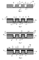
- Figures 1 to 10 illustrate a particular embodiment of a microfluidic component 1 having three closed microchannels 2.
- closed microchannel means a microchannel of microscopic dimensions, having an inlet and an outlet for the passage of a fluid, but delimited not only by a bottom wall 3 forming the bottom of the microchannel 2 and by two opposite side walls 4 and 5. but also by an upper wall 6.
- the distance P between the lower 3 and upper 6 walls is between 5 ⁇ m and 100 ⁇ m while the distance L between the two opposite side walls 4 and 5 is preferably between 1 ⁇ m and 500 ⁇ m.
- the bottom wall 3 and the two opposite side walls 4 and 5 of each microchannel 2 are formed in a substrate 7, for example in a silicon wafer having a thickness of the order of 450 micrometers, and a diameter of 100mm.
- the three microchannels 2 are, for example, formed by selective etching in a substrate 7 having a free surface 7a.
- the totality of the free surface 7a is, on the figure 1 covered with a layer 8 of photosensitive resin.
- the layer 8 is structured in the form of patterns 8a by photolithography. So, the reasons 8a are formed by irradiating the layer 8 by UV radiation (arrows F1), through a mask 9, then removing the exposed areas of the layer 8. Then, as shown in FIG.
- the substrate 7 undergoes a deep etching step, for example by deep reactive ion etching (DRIE or "Deep Reactive Ion Etching”).
- the etching step is said to be selective, insofar as the etching of the substrate 7 is carried out only at the regions of the substrate 7 not covered by the patterns 8a. So, as represented on the figure 5 , it makes it possible to form, in the surface 7a of the substrate 7, openings (or grooves) delimited in the substrate 7, by surfaces forming the side walls 4 and 5 and the bottom wall 3 of each microchannel 2.
- the patterns 8a of the photosensitive layer are eliminated, thus releasing the surface 7a of the substrate 7 provided with said microchannels 2.
- a step of depositing a metal catalyst is then carried out.
- the side walls 4 and 5 and the bottom wall 3 of each microchannel 2 are covered with a metal catalyst layer 9.
- the free surface 7a of the substrate 7 is also covered with metal catalyst.
- a layer 10 constituted by the same metal catalyst thus covers said surface 7a. It is advantageously deposited at the same time as the layer 9 covering the side walls 4 and 5 and the bottom wall 3 of the microchannels.
- the metal forming the metal catalyst is preferably selected from nickel, cobalt, iron and gold and can be deposited by a physical deposition technique, for example by spraying or by evaporation, or by a technique chemical or electrolytic deposition. According to the technique used, the deposition conditions are optimized in order to obtain a metal catalyst layer 10 on the free surface 7a of the substrate 7, of a thickness e sufficient to carry out the subsequent sealing step and a metallic catalyst layer. 9 on the side walls 4 and 5 of a thickness e 'compatible with the growth of nanostructures.
- the thickness e of the metal catalyst layer 10, deposited on the free surface 7a of the substrate 7, is preferably between 20 nm and 200 nm while the thickness e 'of the metal catalyst layer 9 deposited on the side walls 4 and 5 is advantageously between 1 nm and 20 nm.
- the metal catalyst layer 10 is then used to seal between a protective cover 11 and the substrate 7, before the formation of nanostructures (for example carbon nanotubes).
- the seal is therefore produced by forming a eutectic compound between the metal of the metal catalyst layer 10 and a material of the cover 11.
- the material of the cover 11 is advantageously chosen from silicon, silicon oxide and glass.
- the protective cover 11 is put in place or placed on the layer 10 covering the surface 7a of the substrate 7 (arrows F2), so that the face 11a of the cover 11, advantageously flat, comes into contact with the surface 7a of the substrate 7 and more particularly with the layer 10 disposed on the surface 7a.
- a heat treatment (arrows F3) is performed at a predetermined temperature to obtain the diffusion of the metal contained in the layer 10 to the cover 11 and the formation of a eutectic compound 12 between said metal and a material of the cover.
- the face 11a of the cover 11 has portions in contact with the surface 7a and portions disposed opposite the microchannels 7. Said portions of the face 11a arranged opposite microchannels 7 form, then, the upper walls 6 of said microchannels 2 and thus allow them to be closed.
- the seal may be obtained by producing a heat treatment for forming a nickel silicide.
- a sealing technique is, for example, known to seal two silicon wafers by forming a nickel silicide at a heat treatment temperature of 440 ° C, as reported. Zhi-Xiong Xiao et al. in the article "Low temperature silicon wafer-to-wafer bonding with nickel silicide” (J.Electrochem Soc., Vol 145, No. 4, April 1998 ).
- the metal used for sealing also serves as a metal catalyst for forming the nanostructures in the microchannels 2.
- the metal catalyst layer 9 deposited on the figure 6 , on the side walls 4 and 5 and on the bottom wall 3 then makes it possible to catalyze the growth of nanostructures such as carbon nanotubes.
- the carbon nanotubes are, for example, obtained by chemical vapor deposition (CVD) carried out at a temperature of 700 ° C. under atmospheric pressure and using acetylene as carbonaceous gas.
- CVD chemical vapor deposition
- acetylene as carbonaceous gas.
- nanostructures 13a join the nanostructures 13b, as shown in FIG. figure 10 in order to fill the microchannels 2.
- a subsequent cutting step can then be performed to form microreactors each provided with one or more microchannels 2 completely filled with nanostructures.
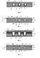
- an additional metal catalyst layer 14 is deposited on the entire face 11a of the cover 11.
- the face 11a of the cover 11 is the face intended to come into contact with the surface 7a of the substrate 7, when the place of said cover on the surface 7a of the substrate 7.
- the portions of the face 11 disposed facing microchannels 2 and forming the upper walls 6 of said microchannels 2 remain covered by metal catalyst and can therefore be the seat of in situ growth of nanostructures 13d, from the catalyst layer Additional metal 14. Nanostructures 13d are then formed on the upper wall 6 of each microchannel 2.
- microchannels are thus closed before the growth of nanostructures.
- the growth of the nanostructures, obtained by in situ growth remains homogeneous, despite the closure of the microchannels.
- Such a method is compatible with a method for producing collective components on wafer wafers. requires no post-growth technological step, which avoids any possible contamination of the external environment to the component, such as deposit chambers and clean rooms used to make these deposits or the operator present during the process.
- the microchannel (s) 2 of the microfluidic component may have any type of geometry.
- their input can be connected to a fluid division zone, itself connected to an input microchannel while their output can be connected to a fluid collecting zone, itself connected to an output microchannel. .
Landscapes
- Chemical & Material Sciences (AREA)
- Health & Medical Sciences (AREA)
- Chemical Kinetics & Catalysis (AREA)
- Engineering & Computer Science (AREA)
- General Health & Medical Sciences (AREA)
- Life Sciences & Earth Sciences (AREA)
- Clinical Laboratory Science (AREA)
- Hematology (AREA)
- Analytical Chemistry (AREA)
- Molecular Biology (AREA)
- Dispersion Chemistry (AREA)
- Manufacturing & Machinery (AREA)
- Microelectronics & Electronic Packaging (AREA)
- Organic Chemistry (AREA)
- Micromachines (AREA)
- Physical Or Chemical Processes And Apparatus (AREA)
- Carbon And Carbon Compounds (AREA)
Abstract
Description
- L'invention concerne un procédé de fabrication d'un composant microfluidique comportant au moins un microcanal délimité par des parois inférieure et supérieure et deux parois latérales opposées, procédé comportant :
- la formation, dans une surface d'un substrat, de la paroi inférieure et des deux parois latérales opposées dudit microcanal,
- la formation, par croissance in situ à partir d'une couche de catalyseur métallique déposée sur les parois latérales opposées et sur la paroi inférieure dudit microcanal, de nanostructures remplissant ledit microcanal
- et la formation de la paroi supérieure dudit microcanal par mise en place d'un capot sur ladite surface du substrat et scellement dudit capot sur ladite surface.
- Les composants microfluidiques, également appelés microsystèmes fluidiques, tels que les microréacteurs ou bien les microlaboratoires plus connus sous les noms anglo-saxons de « µ-TAS » (micro Total Analysis System) ou de « Lab-on-a-chip », connaissent un réel essor depuis une dizaine d'années, pour réaliser des opérations et/ou des analyses chimiques ou biologiques, sur des échantillons de très petits volumes. L'utilisation de ces composants peut, en effet, permettre d'intégrer différentes étapes sur un même composant (injection, séparation, détection), limitant alors le nombre de connections et donc la perte des échantillons durant les différentes manipulations, tout en augmentant la sensibilité d'analyse et en diminuant la durée d'analyse.
- Or, on cherche à intégrer un nombre croissant de fonctions dans ces composants microfluidiques. À titre d'exemple, il est souhaitable de réaliser des composants microfluidiques permettant de réaliser plusieurs opérations telles que des pré-traitements sur un échantillon, des filtrations, des mélanges, des séparations et/ou de la détection. Une telle intégration nécessite, cependant, des composants permettant d'obtenir des performances toujours plus grandes en termes de miniaturisation et/ou d'efficacité. De plus, il est connu que l'efficacité d'une réaction chimique ou biologique hétérogène ou d'une séparation est d'autant plus élevée que le rapport entre la surface du composant en contact avec l'échantillon et le volume d'échantillon circulant dans ledit composant, appelé également rapport S/V, est élevé.
- Les approches les plus classiques pour obtenir un rapport S/V élevé consistent à remplir des microcanaux formés dans des composants microfluidiques par des structures poreuses ou phases stationnaires, telles que les billes de silice.
- Ainsi, dans l'article « High performance liquid chromatography partially integrated onto a silicon chip » de Gregor Ocvirk et al. (Analytical Methods and Instrumentation, Vol 2, N°2, 74-82 (1995)), un système de chromatographie liquide est réalisé en formant un réseau de microcanaux, remplis d'un matériau de remplissage, dans une structure plane (ou puce) en silicium, avec un injecteur à débit divisé (« split injector ») disposé à l'entrée desdits microcanaux, ainsi qu'un fritté et une cellule de détection optique disposés à la sortie desdits microcanaux. Les microcanaux du système sont scellés par un procédé de type scellement anodique, à l'aide d'une couche en verre disposée sur la structure en silicium. Une autre structure en silicium, complétant le système, est scellée par le même procédé de scellement, sur la couche en verre, afin de rendre le système plus résistant.
- Cependant, compte tenu du diamètre des microcanaux, remplir un microcanal de manière homogène avec une phase stationnaire devient une opération difficile à réaliser à l'échelle microscopique. De même, ces composants nécessitent la mise en place de systèmes retenant la phase stationnaire à l'intérieur des microcanaux, tels que des frittés ou des systèmes d'injection. Or, cette opération devient également délicate à cette échelle.
- D'autres approches ont été envisagées pour remédier à ce problème. Il a, par exemple, été proposé de réaliser la phase stationnaire directement dans un microcanal. Ainsi, comme décrit dans l'article « Capillary columns with in situ formed porous monolithic packing for micro high-performance liquid chromatography and capillary electrochromatography » d'Isabelle Gusev et al. (Journal of Chromatography A, 855 (1999) 273-290), la synthèse in-situ d'une phase stationnaire monolithique ancrée sur les parois d'un microcanal permet d'éviter l'utilisation de frittés. Il a aussi été proposé d'utiliser les techniques utilisées dans le domaine de la microélectronique (photolithographie, gravure) pour former par nanostructuration et de façon reproductible et collective, une phase stationnaire à l'intérieur d'un microcanal.
- Par ailleurs, les récents développements dans le domaine des procédés de synthèse de nanostructures, telles que les nanotubes de carbone également appelés NTC ou les nanofibres de carbone, permettent d'envisager de nouvelles perspectives pour développer la surface de contact des composants microfluidiques. Il existe principalement deux voies de développement.
- La première voie consiste à réaliser, à partir de poudres catalytiques, des nanotubes de carbone indépendants, c'est-à-dire non solidaires d'une surface, puis à remplir le composant microfluidique et plus particulièrement le ou les microcanaux dudit composant, avec ces nanotubes de carbone préalablement synthétisés. Des cartouches d'extraction sur phase solide, mais également des colonnes de chromatographie ont ainsi été développées selon ce principe. À titre d'exemple, dans l'article « Electrophoretic separation of aniline derivatives using fused silica capillaries coated with acid treated single-walled carbon nanotubes » de John H.T. Luong et al., (Journal of Chromatography A, 1074 (2005) 187-194), la surface de capillaires en silice fondue est préparée, avant d'être revêtue par des nanotubes de carbone monofeuillets traités à l'acide. Le dépôt de nanotubes sur la surface des capillaires est réalisé en rinçant ladite surface par une solution contenant lesdits nanotubes préalablement synthétisés et traités.
- La seconde voie permet de former les nanotubes de carbone in situ, sur une surface préalablement revêtue d'un dépôt de catalyseur métallique. La croissance des nanotubes peut, alors, être localisée précisément par un simple dépôt sélectif du catalyseur. Cette technique permet également d'éliminer toutes étapes de greffage ou de remplissage du microcanal. À titre d'exemple, Michael Stadermann et al. dans l'article « Ultrafast gas chromatography on single-wall carbon nanotube stationary phases in microfabricated channels » (Anal. Chem. 2006, 78, 5639-5644) décrivent une chromatographie en phase gazeuse ultrarapide sur des phases stationnaires formées par des nanotubes de carbone monofeuillets (SWNTs) dans des microcanaux microstructurés dans une plaquette en silicium. Lesdits nanotubes de carbone monofeuillets sont obtenus par croissance in situ, par dépôt chimique en phase vapeur, à partir d'une couche de catalyseur métallique, par exemple en aluminium, en molybdène ou en fer. De même, la demande
WO-A-2006/122697 décrit un composant microfluidique comportant au moins un microcanal délimité dans un substrat et rempli de nanotubes synthétisés par croissance in situ à partir d'une couche de catalyseur métallique préalablement déposée sur les parois latérales opposées et sur la paroi inférieure dudit microcanal. - Avec cette seconde voie, les nanotubes de carbone sont, généralement, réalisés dans un microcanal sans paroi supérieure, c'est-à-dire un microcanal ouvert (ou rainure). Ceci permet de contrôler l'homogénéité du dépôt de la couche de catalyseur et la croissance des nanotubes. Dans la demande
WO-A-2006/122697 , un capot de protection est, ainsi, disposé, après la formation des nanotubes, sur la surface du substrat pour recouvrir ledit microcanal rempli de nanotubes. Le capot est, ensuite scellé par scellement moléculaire en formant des liaisons de type Si-Si ou de type Si-Verre, de qui rend le microcanal fermé et parfaitement étanche. De même, dans l'article de Michael Stadermann et al., les microcanaux sont fermés en déposant une couche en verre sur la plaquette en silicium et en réalisant un scellement anodique après la formation des nanotubes. - Or, l'étape de scellement du capot, c'est-à-dire la fermeture du microcanal, se révèle être une étape critique dans le procédé de fabrication du composant microfluidique. En effet, le procédé de fabrication doit être compatible avec cette étape de scellement et notamment avec les contraintes qu'elle impose. En général, les nanotubes ne supportent pas les étapes préalables de nettoyage nécessaires pour réaliser le scellement entre deux plaquettes de silicium (« wafer-wafer »), ni les températures élevées sous conditions oxydantes de certaines techniques de scellement. De plus, les nanotubes risquent de polluer les surfaces assurant le scellement et/ou l'atmosphère des machines utilisées lors du procédé de fabrication.
- Une méthode de croissance dans un milieu fermé a bien été proposée par Mahesh Karwa et al., dans l'article « Gas chromatography on self-assembled single-walled carbon nanotubes » ( Anal. Chem. 2006, 78, 2064-2070). Des nanotubes de carbone monofeuillets (SWNTs ou « Single-Walled Carbon Nanotubes ») sont formés dans un tube capillaire en acier inoxydable et dans un tube capillaire en acier inoxydable revêtu de silice, par synthèse catalytique en phase vapeur. Une solution éthanolique, dans laquelle est dissous de l'acétate de molybdène et du nitrate de cobalt hexahydraté, est injectée dans le tube capillaire, en même temps que de l'hydrogène, afin de revêtir le tube d'une couche en catalyseur. Puis, un dépôt chimique en phase vapeur (CVD) est réalisé pour former, par croissance in situ, des nanotubes. Comme le fer contenu dans les tubes capillaires agit comme un catalyseur pour la formation des nanotubes de carbone multifeuillets (MWNTs ou « Multi-Walled Carbon Nanotubes »)), le tube capillaire revêtu de silice est préféré pour réaliser les SWNTs.
- Cependant, un tel procédé de fabrication et notamment le dépôt de catalyseur par l'intermédiaire d'une solution éthanolique n'est pas pratique à mettre en oeuvre, car il nécessite un nombre important de manipulations, et est difficilement adaptable en microsystème.
- Pour éviter les contraintes liées au dépôt de catalyseur, Chutarat Saridara et Somenath Mitra ont proposé dans l'article « Chromatography on Self-Assembled Carbon Nanotubes » (Anal. Chem. 2005, 77, 7094-7097) d'utiliser le fer se trouvant dans les impuretés de l'acier inoxydable du tube capillaire comme catalyseur. Cependant, la formation des nanotubes de carbone s'avère inhomogène le long du tube capillaire.
- L'invention a pour but un procédé de fabrication d'un composant microfluidique remédiant aux inconvénients mentionnés ci-dessus.
- Plus particulièrement, l'invention a pour but un procédé de fabrication permettant d'obtenir, facilement et à faibles coûts, un composant microfluidique comportant au moins un microcanal rempli, de manière homogène, par des nanostructures. Le procédé doit, avantageusement, être compatible avec les procédés de réalisation de composants collectifs sur des plaquettes de type « wafer », tout en évitant de contaminer l'environnement du microcomposant.
- Selon l'invention, ce but est atteint par les revendications annexées.
- En particulier, ce but est atteint par le fait qu'une couche dudit catalyseur métallique est également déposée sur la surface du substrat destinée à venir en contact avec le capot et par le fait que le scellement est réalisé avant la formation des nanostructures, par traitement thermique formant un composé eutectique entre le métal de la couche de catalyseur métallique et un matériau du capot.
- Selon un développement de l'invention, la couche dudit catalyseur métallique est déposée sur la surface du substrat destinée à venir en contact avec le capot en même temps que celle déposée sur les parois latérales opposées et sur la paroi inférieure dudit microcanal.
- Selon un autre développement de l'invention, l'épaisseur de la couche dudit catalyseur métallique déposée sur la surface du substrat destinée à venir en contact avec le capot est comprise entre 20nm et 200nm.
- D'autres avantages et caractéristiques ressortiront plus clairement de la description qui va suivre de modes particuliers de réalisation de l'invention donnés à titre d'exemples non limitatifs et représentés aux dessins annexés, dans lesquels :
- les
figures 1 à 10 représentent, schématiquement et en coupe, différentes étapes successives d'un mode particulier de réalisation d'un procédé de fabrication selon l'invention. - les
figures 11 et 12 représentent, schématiquement et en coupe, des étapes d'une variante de réalisation du mode représenté sur lesfigures 1 à 10 . - Un composant microfluidique, également appelé microsystème fluidique, comporte au moins un microcanal fermé permettant le passage d'un fluide. Ledit microcanal est délimité par des parois inférieure et supérieure et deux parois latérales opposées et il est rempli de nanostructures, telles que des nanotubes et en particulier des nanotubes de carbone.
- Le composant est réalisé en formant, préalablement, dans une surface d'un substrat, par exemple en silicium, en oxyde de silicium ou en verre, la paroi inférieure et les deux parois latérales opposées dudit microcanal. La formation de la paroi supérieure dudit microcanal est réalisée en mettant en place un capot comportant, par exemple, un matériau choisi parmi le silicium, l'oxyde de silicium et le verre, sur ladite surface du substrat et en scellant le capot sur ladite surface. Puis, les nanostructures remplissant le microcanal sont formées par croissance in situ à partir d'une couche de catalyseur métallique déposée sur les parois latérales opposées et sur la paroi inférieure dudit microcanal.
- Ainsi, contrairement aux procédés de fabrication décrits dans l'art antérieur et plus particulièrement le procédé décrit dans la demande de brevet
WO-A-2006/122697 , la paroi supérieure du microcanal est formée avant la formation des nanostructures. Plus particulièrement, une couche du même catalyseur métallique que celui utilisé pour la formation des nanostructures est également déposée sur le substrat. Ladite couche est, plus particulièrement, déposée sur la surface du substrat, destinée à venir en contact avec le capot. Le scellement est, alors, obtenu avant la formation des nanostructures, en réalisant un traitement thermique permettant de former un composé eutectique. Le composé eutectique est un composé eutectique entre le métal de la couche de catalyseur métallique et un matériau du capot ou avantageusement le matériau constituant ledit capot. - À titre d'exemple, les
figures 1 à 10 illustrent un mode particulier de réalisation d'un composant microfluidique 1 comportant trois microcanaux 2 fermés. Par microcanal fermé, on entend un microcanal de dimensions microscopiques, comportant une entrée et une sortie pour le passage d'un fluide, mais délimité non seulement par une paroi inférieure 3 formant le fond du microcanal 2 et par deux parois latérales opposées 4 et 5 mais également par une paroi supérieure 6. Avantageusement, la distance P entre les parois inférieure 3 et supérieure 6 est comprise entre 5µm et 100µm tandis que la distance L entre les deux parois latérales 4 et 5 opposées est, de préférence, comprise entre 1 µm et 500µm. - La paroi inférieure 3 et les deux parois latérales opposées 4 et 5 de chaque microcanal 2 sont formées dans un substrat 7, par exemple dans une plaquette en silicium (« wafer ») d'une épaisseur de l'ordre de 450 micromètres et d'un diamètre de 100mm.
- Ainsi, comme représentés sur les
figures 1 à 5 , les trois microcanaux 2 sont, par exemple, formés par gravure sélective dans un substrat 7 comportant une surface libre 7a. Pour réaliser la gravure sélective, la totalité de la surface libre 7a est, sur lafigure 1 , recouverte d'une couche 8 en résine photosensible. Puis, comme représenté sur lesfigures 2 et 3 , la couche 8 est structurée sous forme de motifs 8a par photolithographie. Ainsi, les motifs 8a sont formés en insolant la couche 8 par rayonnements UV (flèches F1), à travers un masque 9, puis en éliminant les zones insolées de la couche 8. Ensuite, comme illustré sur lafigure 4 , le substrat 7 subit une étape de gravure profonde, par exemple par gravure ionique réactive profonde (DRIE ou "Deep Reactive Ion Etching"). L'étape de gravure est dite sélective, dans la mesure où la gravure du substrat 7 est réalisée uniquement au niveau des zones du substrat 7 non recouvertes par les motifs 8a. Ainsi, comme représenté sur lafigure 5 , elle permet de former, dans la surface 7a du substrat 7, des ouvertures (ou des rainures) délimitées, dans le substrat 7, par des surfaces formant les parois latérales 4 et 5 et la paroi inférieure 3 de chaque microcanal 2. Une fois le substrat 7 gravé, les motifs 8a de la couche photosensible sont éliminés, libérant, ainsi, la surface 7a du substrat 7 munie desdits microcanaux 2. - Comme représenté sur la
figure 6 , une étape de dépôt d'un catalyseur métallique est ensuite réalisée. Les parois latérales 4 et 5 et la paroi inférieure 3 de chaque microcanal 2 sont recouvertes d'une couche 9 en catalyseur métallique. De plus, la surface libre 7a du substrat 7 est également recouverte de catalyseur métallique. Une couche 10 constituée par le même catalyseur métallique recouvre donc ladite surface 7a. Elle est, avantageusement, déposée en même temps que la couche 9 recouvrant les parois latérales 4 et 5 et la paroi inférieure 3 des microcanaux. - Le métal formant le catalyseur métallique est, de préférence, choisi parmi le nickel, le cobalt, le fer et l'or et il peut être déposé par une technique de dépôt physique, par exemple par pulvérisation ou par évaporation, ou bien par une technique de dépôt chimique ou électrolytique. Selon la technique utilisée, les conditions de dépôt sont optimisées afin d'obtenir une couche de catalyseur métallique 10 sur la surface libre 7a du substrat 7, d'une épaisseur e suffisante pour réaliser l'étape ultérieure de scellement et une couche de catalyseur métallique 9 sur les parois latérales 4 et 5 d'une épaisseur e' compatible avec la croissance de nanostructures. L'épaisseur e de la couche de catalyseur métallique 10, déposée sur la surface libre 7a du substrat 7, est, de préférence, comprise entre 20nm et 200nm tandis que l'épaisseur e' de la couche de catalyseur métallique 9, déposée sur les parois latérales 4 et 5 est, avantageusement, comprise entre 1 nm et 20nm.
- Ainsi, comme représenté sur les
figures 7 à 9 , la couche de catalyseur métallique 10 est, ensuite, utilisée, pour réaliser le scellement entre un capot de protection 11 et le substrat 7, avant la formation des nanostructures ( par exemple des nanotubes de carbone). - Le scellement est, donc, réalisé en formant un composé eutectique entre le métal de la couche en catalyseur métallique 10 et un matériau du capot 11. Le matériau du capot 11 est, avantageusement, choisi parmi le silicium, l'oxyde de silicium et le verre. Comme représenté sur la
figure 7 , le capot de protection 11 est mis en place ou disposé sur la couche 10 recouvrant la surface 7a du substrat 7 (flèches F2), de sorte que la face 11a du capot 11, avantageusement plane, entre en contact avec la surface 7a du substrat 7 et plus particulièrement avec la couche 10 disposée sur la surface 7a. Puis, comme illustré sur lafigure 8 , un traitement thermique (flèches F3) est réalisé à une température prédéterminée permettant d'obtenir la diffusion du métal contenu dans la couche 10 vers le capot 11 et la formation d'un composé eutectique 12 entre ledit métal et un matériau du capot. Ainsi, une fois le capot de protection 11 scellé sur le substrat 7, la face 11 a du capot 11 comporte des portions en contact avec la surface 7a et des portions disposées en regard des microcanaux 7. Lesdites portions de la face 11a disposées en regard des microcanaux 7 forment, alors, les parois supérieures 6 desdits microcanaux 2 et permettent donc de les fermer. - À titre d'exemple, pour une couche 10 en nickel et un capot 11 en silicium ou en oxyde de silicium, le scellement peut être obtenu en réalisant un traitement thermique permettant de former un siliciure de nickel. Une telle technique de scellement est, par exemple, connue pour sceller deux plaquettes en silicium par formation d'un siliciure de nickel à une température de traitement thermique de 440°C, comme le rapportent Zhi-Xiong Xiao et al. dans l'article « Low temperature silicon wafer-to-wafer bonding with nickel silicide » (J.Electrochem. Soc., Vol 145, N°4, April 1998).
- Dans le cadre de la présente invention, le métal utilisé pour réaliser le scellement sert également de catalyseur métallique pour réaliser la formation des nanostructures, dans les microcanaux 2. Ainsi, la couche de catalyseur métallique 9 déposée, sur la
figure 6 , sur les parois latérales 4 et 5 et sur la paroi inférieure 3 permet, ensuite, de catalyser la croissance des nanostructures telles que des nanotubes de carbone. Les nanotubes de carbone sont, par exemple, obtenus par dépôt chimique en phase vapeur (CVD) réalisé à une température de 700°C, sous pression atmosphérique et en utilisant de l'acétylène comme gaz carboné. Ainsi, dans un même cycle thermique, trois ensembles de nanostructures, respectivement 13a, 13b et 13c, sont formés sur lafigure 10 par croissance, approximativement perpendiculairement aux parois respectives 4, 5 et 3. Il est, de plus, avantageusement, possible d'obtenir qu'une majorité des nanostructures 13a rejoigne les nanostructures 13b, comme représenté à lafigure 10 , de manière à remplir les microcanaux 2. Une étape ultérieure de découpe peut ensuite être réalisée pour former des microréacteurs munis chacun d'un ou de plusieurs microcanaux 2 complètement remplis de nanostructures. - Dans une variante de réalisation représentée sur les
figures 11 et 12 , une couche de catalyseur métallique supplémentaire 14 est déposée sur la totalité de la face 11 a du capot 11. La face 11 a du capot 11 est la face destinée à venir en contact avec la surface 7a du substrat 7, lors de la mise en place dudit capot sur la surface 7a du substrat 7. Ainsi, une fois le capot mis en place sur la surface 7a du substrat 7 et le scellement réalisé, les portions de la face 11 a disposées en regard des microcanaux 2 et formant les parois supérieures 6 desdits microcanaux 2 restent couvertes par du catalyseur métallique et peuvent donc être le siège d'une croissance in situ de nanostructures 13d, à partir de la couche de catalyseur métallique supplémentaire 14. Des nanostructures 13d sont alors formées sur la paroi supérieure 6 de chaque microcanal 2. - Le procédé de réalisation d'un composant microfluidique selon l'invention permet, ainsi, d'utiliser un métal jouant une double fonction :
- précurseur pour le scellement entre le capot et le substrat
- et catalyseur pour la croissance des nanostructures.
- Les microcanaux sont donc fermés avant la croissance de nanostructures. Cependant, avec un tel procédé de fabrication, la croissance des nanostructures, obtenue par croissance in situ, reste homogène, malgré la fermeture des microcanaux.
- Enfin, un tel procédé est compatible avec un procédé de réalisation de composants collectif sur des plaquettes en silicium (« wafer ») et il ne nécessite pas d'étape technologique post-croissance, ce qui évite toute contamination éventuelle de l'environnement extérieur au composant, tel que les enceintes de dépôt et les salles blanches utilisées pour réaliser ces dépôts ou l'opérateur présent lors du procédé.
- Un composant microfluidique obtenu par un tel procédé peut être utilisé dans diverses applications. À titre d'exemple, il peut être employé comme :
- support de décomposition catalytique : Si les parois des nanostructures sont recouvertes par un dépôt de platine, le microcomposant peut, par exemple, être utilisé pour réaliser l'oxydation complète du CO en CO2 par l'oxygène à plus basse température.
- support de greffage d'enzyme : des nanotubes de carbone peuvent être facilement fonctionnalisés : les nanotubes peuvent être greffés par une enzyme telle que la trypsine afin d'utiliser le microcomposant pour la digestion de protéines,
- support de phase stationnaire : des nanotubes de carbone constituent une phase stationnaire directement utilisable pour des applications en chromatographie, ils peuvent également être fonctionnalisés par diverses molécules chimiques.
- L'invention n'est pas limitée aux modes de réalisation représentés sur les
figures 1 à 12 . À titre d'exemple, le ou les microcanaux 2 du composant microfluidique peuvent avoir tout type de géométrie. De plus, leur entrée peut être connectée à une zone de division du fluide, elle-même connectée à un microcanal d'entrée tandis que leur sortie peut être connectée à une zone de rassemblement du fluide, elle-même connectée à un microcanal de sortie.
Claims (10)
- Procédé de fabrication d'un composant microfluidique (1) comportant au moins un microcanal (2) délimité par des parois inférieure (3) et supérieure (6) et deux parois latérales opposées (4, 5), procédé comportant :- la formation, dans une surface (7a) d'un substrat (7), de la paroi inférieure (3) et des deux parois latérales (4, 5) opposées dudit microcanal (2),- la formation, par croissance in situ à partir d'une couche de catalyseur métallique (9) déposée sur les parois latérales opposées (4, 5) et sur la paroi inférieure (3) dudit microcanal (2), de nanotstructures (13a, 13b, 13c) remplissant ledit microcanal (2)- et la formation de la paroi supérieure (6) dudit microcanal (2) par mise en place d'un capot (11) sur ladite surface (7a) du substrat (7) et scellement dudit capot (11) sur ladite surface (7a),
procédé caractérisé en ce qu'une couche (10) dudit catalyseur métallique est également déposée sur la surface (7a) du substrat (7) destinée à venir en contact avec le capot (11) et en ce que le scellement est réalisé avant la formation des nanostructures (13a, 13b, 13c), par traitement thermique formant un composé eutectique (12) entre le métal de la couche de catalyseur métallique (10) et un matériau du capot (11). - Procédé selon la revendication 1, caractérisé en ce que la couche (10) dudit catalyseur métallique est déposée sur la surface (7a) du substrat (7) destinée à venir en contact avec le capot (11) en même temps que celle déposée sur les parois latérales opposées (4, 5) et sur la paroi inférieure (3) dudit microcanal (2).
- Procédé selon l'une des revendications 1 et 2, caractérisé en ce que l'épaisseur (e) de la couche dudit catalyseur métallique (10) déposée sur la surface (7a) du substrat (7) destinée à venir en contact avec le capot (11) est comprise entre 20nm et 200nm.
- Procédé selon l'une quelconque des revendications 1 à 3, caractérisé en ce que l'épaisseur (e') de la couche (9) déposée sur les parois latérales opposées et sur la paroi inférieure (3) dudit microcanal (2) est comprise entre 1 nm et 20nm.
- Procédé selon l'une quelconque des revendications 1 à 4, caractérisé en ce que des nanostructures (13d) sont formées sur la paroi supérieure (6) du microcanal (2), par croissance in situ à partir d'une couche de catalyseur métallique supplémentaire (14) déposée sur ladite paroi (6).
- Procédé selon la revendication 5, caractérisé en ce que la couche de catalyseur métallique supplémentaire (14) est déposée sur la totalité de la face (11a) du capot (11), destinée à venir en contact avec la surface (7a) du substrat (7) lors de la mise en place dudit capot (11).
- Procédé selon l'une quelconque des revendications 1 à 6, caractérisé en ce que le catalyseur métallique est choisi parmi le nickel, le cobalt, le fer et l'or.
- Procédé selon l'une quelconque des revendications 1 à 7, caractérisé en ce que le matériau du capot (11) est choisi parmi le silicium, l'oxyde de silicium et le verre.
- Procédé selon l'une quelconque des revendications 1 à 8, caractérisé en ce que la distance (L) entre les deux parois latérales opposées (4, 5) du microcanal (2) est comprise entre 1µm et 500µm.
- Procédé selon l'une quelconque des revendications 1 à 9, caractérisé en ce que la distance (P) entre les parois supérieure (6) et inférieure (3) du microcanal (2) est comprise entre 5µm et 100µm.
Applications Claiming Priority (1)
| Application Number | Priority Date | Filing Date | Title |
|---|---|---|---|
| FR0706837A FR2921648A1 (fr) | 2007-09-28 | 2007-09-28 | Procede de fabrication d'un composant microfluidique comportant au moins un microcanal rempli de nanostructures. |
Publications (2)
| Publication Number | Publication Date |
|---|---|
| EP2042467A1 true EP2042467A1 (fr) | 2009-04-01 |
| EP2042467B1 EP2042467B1 (fr) | 2010-03-17 |
Family
ID=39436882
Family Applications (1)
| Application Number | Title | Priority Date | Filing Date |
|---|---|---|---|
| EP08354060A Not-in-force EP2042467B1 (fr) | 2007-09-28 | 2008-09-04 | Procédé de fabrication d'un composant microfluidique comportant au moins un microcanal rempli de nanostructures |
Country Status (7)
| Country | Link |
|---|---|
| US (1) | US8029863B2 (fr) |
| EP (1) | EP2042467B1 (fr) |
| JP (1) | JP5225796B2 (fr) |
| CN (1) | CN101458260B (fr) |
| AT (1) | ATE461153T1 (fr) |
| DE (1) | DE602008000830D1 (fr) |
| FR (1) | FR2921648A1 (fr) |
Cited By (1)
| Publication number | Priority date | Publication date | Assignee | Title |
|---|---|---|---|---|
| US9291567B2 (en) | 2011-03-15 | 2016-03-22 | Lidija Malic | Microfluidic system having monolithic nanoplasmonic structures |
Families Citing this family (21)
| Publication number | Priority date | Publication date | Assignee | Title |
|---|---|---|---|---|
| EP2152417B1 (fr) | 2007-05-04 | 2018-07-11 | Opko Diagnostics, LLC | Dispositif et méthode pour analyses dans des systèmes microfluidiques |
| WO2010087999A1 (fr) * | 2009-02-02 | 2010-08-05 | Claros Diagnostics, Inc. | Structures pour le contrôle des interactions de la lumière avec des dispositifs microfluidiques |
| CN102341693B (zh) * | 2009-03-07 | 2013-11-20 | 惠普开发有限公司 | 分析器和使用该分析器进行感测的方法 |
| US20110011157A1 (en) * | 2009-07-16 | 2011-01-20 | Bertrand Bourlon | Gas chromatograph column with carbon nanotube-bearing channel |
| WO2011154363A2 (fr) * | 2010-06-07 | 2011-12-15 | Commissariat à l'énergie atomique et aux énergies alternatives | Dispositif d'analyse comportant un réseau mems et/ou nems |
| CA2801541C (fr) | 2010-06-07 | 2018-05-15 | Commissariat A L'energie Atomique Et Aux Energies Alternatives | Systeme pour l'analyse d'un melange gazeux comprenant au moins une colonne de chromatographie |
| CN102259825B (zh) * | 2011-06-17 | 2015-04-08 | 清华大学 | 一种mems原子蒸气腔室的制备方法及原子蒸气腔室 |
| CN108108590A (zh) | 2012-03-05 | 2018-06-01 | 阿克蒂克合伙公司 | 分析系统和方法 |
| US9139416B2 (en) * | 2012-08-01 | 2015-09-22 | University Of South Carolina | Microfluidic devices for the generation of nano-vapor bubbles and their methods of manufacture and use |
| CN103769252B (zh) * | 2012-10-18 | 2016-01-27 | 中国科学院深圳先进技术研究院 | 微流控芯片的连接器 |
| CN103424429B (zh) * | 2013-06-25 | 2016-04-06 | 复旦大学 | 基于纳米管微系统的分子筛选方法及纳米管微系统芯片 |
| KR101392426B1 (ko) | 2013-07-08 | 2014-05-07 | 한국기계연구원 | 마이크로 채널 소자 및 마이크로 채널 소자의 제작방법 |
| CN104083930B (zh) * | 2014-07-04 | 2015-10-28 | 中国科学院苏州纳米技术与纳米仿生研究所 | 一种过滤芯片及其加工制作方法 |
| CN104587930B (zh) * | 2014-12-24 | 2017-10-27 | 东南大学 | 金属/碳纳米管复合纳米线的合成及专用微/纳米反应器 |
| US9719926B2 (en) | 2015-11-16 | 2017-08-01 | International Business Machines Corporation | Nanopillar microfluidic devices and methods of use thereof |
| JP2017122600A (ja) * | 2016-01-05 | 2017-07-13 | 富士電機株式会社 | マイクロチップ及びマイクロチップの製造方法 |
| CN108405005B (zh) * | 2018-05-30 | 2024-08-13 | 深圳先进技术研究院 | 一种用于防止纳米通道键合密封堵塞的填充阻隔器 |
| CN109941958B (zh) * | 2018-12-30 | 2023-02-17 | 深圳博华仕科技有限公司 | 一种微流道芯片的填充装置 |
| CN111320133B (zh) * | 2020-02-27 | 2022-03-25 | 西人马联合测控(泉州)科技有限公司 | 芯片的分离方法以及晶圆 |
| JP2020197544A (ja) * | 2020-09-17 | 2020-12-10 | 国立大学法人鳥取大学 | 吸着装置及び分析装置 |
| CN114177959A (zh) * | 2021-12-16 | 2022-03-15 | 清华大学 | 一种基于碳纳米管的纳流控芯片的制备方法 |
Citations (2)
| Publication number | Priority date | Publication date | Assignee | Title |
|---|---|---|---|---|
| US20040096992A1 (en) * | 2002-11-18 | 2004-05-20 | Harris James M. | Method for producing and testing a corrosion-resistant channel in a silicon device |
| WO2006122697A1 (fr) | 2005-05-17 | 2006-11-23 | Commissariat A L'energie Atomique | Composant microfluidique comprenant au moins un canal rempli de nanotubes et procede de production d'un tel composant microfluidique |
Family Cites Families (6)
| Publication number | Priority date | Publication date | Assignee | Title |
|---|---|---|---|---|
| JP3139339B2 (ja) * | 1995-09-13 | 2001-02-26 | 株式会社村田製作所 | 真空封止デバイスおよびその製造方法 |
| JP2000015804A (ja) * | 1998-06-30 | 2000-01-18 | Ricoh Co Ltd | インクジェットヘッド及びその製造方法 |
| ATE276044T1 (de) * | 1999-08-12 | 2004-10-15 | Ut Battelle Llc | Mikrofluid-vorrichtungen zur gesteuerten handhabung von kleinstvolumen |
| JP2005061997A (ja) * | 2003-08-12 | 2005-03-10 | Canon Inc | 分離用素子及び分離用素子の製造方法 |
| US7238594B2 (en) * | 2003-12-11 | 2007-07-03 | The Penn State Research Foundation | Controlled nanowire growth in permanent, integrated nano-templates and methods of fabricating sensor and transducer structures |
| US20070110639A1 (en) * | 2005-10-14 | 2007-05-17 | Pennsylvania State University | System and method for positioning and synthesizing of nanostructures |
-
2007
- 2007-09-28 FR FR0706837A patent/FR2921648A1/fr not_active Withdrawn
-
2008
- 2008-09-04 DE DE602008000830T patent/DE602008000830D1/de active Active
- 2008-09-04 AT AT08354060T patent/ATE461153T1/de not_active IP Right Cessation
- 2008-09-04 EP EP08354060A patent/EP2042467B1/fr not_active Not-in-force
- 2008-09-08 US US12/230,924 patent/US8029863B2/en not_active Expired - Fee Related
- 2008-09-26 JP JP2008247639A patent/JP5225796B2/ja not_active Expired - Fee Related
- 2008-09-28 CN CN2008102098846A patent/CN101458260B/zh not_active Expired - Fee Related
Patent Citations (2)
| Publication number | Priority date | Publication date | Assignee | Title |
|---|---|---|---|---|
| US20040096992A1 (en) * | 2002-11-18 | 2004-05-20 | Harris James M. | Method for producing and testing a corrosion-resistant channel in a silicon device |
| WO2006122697A1 (fr) | 2005-05-17 | 2006-11-23 | Commissariat A L'energie Atomique | Composant microfluidique comprenant au moins un canal rempli de nanotubes et procede de production d'un tel composant microfluidique |
Non-Patent Citations (8)
| Title |
|---|
| "Gas chromatography on self-assembled single-walled carbon nanotubes", ANAL. CHEM., vol. 78, 2006, pages 2064 - 2070 |
| "Ultrafast gas chromatography on single-wall carbon nanotube stationary phases in microfabricated channels", ANAL. CHEM., vol. 78, 2006, pages 5639 - 5644 |
| CHUTARAT SARIDARA; SOMENATH MITRA: "Chromatography on Self-Assembled Carbon Nanotubes", ANAL. CHEM., vol. 77, 2005, pages 7094 - 7097 |
| FONVERNE ET AL: "In situ synthesized carbon nanotubes as a new nanostructured stationary phase for microfabricated liquid chromatographic column", SENSORS AND ACTUATORS B, vol. 129, no. 2, 7 September 2007 (2007-09-07), ELSEVIER SEQUOIA S.A., LAUSANNE, CH, pages 510 - 517, XP022479447, ISSN: 0925-4005 * |
| GREGOR OCVIRK ET AL.: "High performance liquid chromatography partially integrated onto a silicon chip", ANALYTICAL METHODS AND INSTRUMENTATION, vol. 2, no. 2, 1995, pages 74 - 82 |
| ISABELLE GUSEV ET AL.: "Capillary columns with in situ formed porous monolithic packing for micro high-performance liquid chromatography and capillary electrochromatography", JOURNAL OF CHROMATOGRAPHY A, vol. 855, 1999, pages 273 - 290, XP004180035, DOI: doi:10.1016/S0021-9673(99)00697-4 |
| JOHN H.T. LUONG ET AL.: "Electrophoretic separation of aniline derivatives using fused silica capillaries coated with acid treated single-walled carbon nanotubes", JOURNAL OF CHROMATOGRAPHY A, vol. 1074, 2005, pages 187 - 194 |
| ZHI-XIONG XIAO ET AL.: "Low temperature silicon wafer-to-wafer bonding with nickel silicide", J.ELECTROCHEM. SOC., vol. 145, no. 4, April 1998 (1998-04-01), XP009044880 |
Cited By (1)
| Publication number | Priority date | Publication date | Assignee | Title |
|---|---|---|---|---|
| US9291567B2 (en) | 2011-03-15 | 2016-03-22 | Lidija Malic | Microfluidic system having monolithic nanoplasmonic structures |
Also Published As
| Publication number | Publication date |
|---|---|
| CN101458260A (zh) | 2009-06-17 |
| ATE461153T1 (de) | 2010-04-15 |
| EP2042467B1 (fr) | 2010-03-17 |
| JP5225796B2 (ja) | 2013-07-03 |
| JP2009142976A (ja) | 2009-07-02 |
| DE602008000830D1 (de) | 2010-04-29 |
| FR2921648A1 (fr) | 2009-04-03 |
| CN101458260B (zh) | 2013-06-05 |
| US8029863B2 (en) | 2011-10-04 |
| US20090084496A1 (en) | 2009-04-02 |
Similar Documents
| Publication | Publication Date | Title |
|---|---|---|
| EP2042467B1 (fr) | Procédé de fabrication d'un composant microfluidique comportant au moins un microcanal rempli de nanostructures | |
| CN101175991B (zh) | 带有填充纳米管的通道的微流控器件及其生产方法 | |
| CA2568805C (fr) | Dispositif de manipulation de gouttes destine a l'analyse biochimique, procede de fabrication du dispositif, et systeme d'analyse microfluidique | |
| FR2846957A1 (fr) | Micro-systeme a remplissage de micro-billes et procede d'obtention | |
| FR2964094A1 (fr) | Assemblage d'objets par l'intermediaire d'un cordon de scellement comportant des composes intermetalliques | |
| FR2841380A1 (fr) | Procede d'encapsulation d'un objet sous atmosphere controlee | |
| Contento et al. | Electrolysis in nanochannels for in situ reagent generation in confined geometries | |
| EP1677913A1 (fr) | Dispositif de travail comprenant une zone localisee de capture d'une goutte d un liquide d'interet | |
| CN100554496C (zh) | 制造其工作需要非蒸散型吸气材料的器件的方法 | |
| JP2007533467A (ja) | ナノチャンネルを製造する方法およびこの方法で製造したナノチャンネル | |
| EP1707531B1 (fr) | Procédé de fabrication de micro-canaux enterrés et micro-dispotif comprenant de tels micro-canaux | |
| Gielens et al. | High-flux palladium-silver alloy membranes fabricated by microsystem technology | |
| FR2865806A1 (fr) | Laboratoire sur puce comprenant un reseau micro-fluidique et un nez d'electronebulisation coplanaires | |
| Behrmann et al. | A microfluidic porous solid phase suitable for mass production | |
| US7703313B2 (en) | Conformal film micro-channels for a fluidic micro analyzer | |
| EP4271989A1 (fr) | Structures de colonne | |
| Candler et al. | Encapsulation by film deposition | |
| US20260139299A1 (en) | Methods of fabricating high-throughput arrays with customizable properties using silica microsphere assisted patterning | |
| US11854762B1 (en) | MEMS sample holder, packaged product thereof, and apparatus of charged-particle beam such as electron microscope using the same | |
| Lin et al. | Easily detachable glass bonding in microfluidic device based on hydrophilic interactions | |
| JP2025537397A (ja) | ガスクロマトグラフ、カラム及び製造方法 | |
| Teluchina-Appadu | Surfactant Adsorption on Pt Nanoparticles and its Impact on Catalysis | |
| EP2072458B1 (fr) | Procédé de formation de catalyseur de croissance de nanotubes/nanofibres et de croissance horizontale de nanotubes/nanofibres | |
| De Mas et al. | Nested potassium hydroxide etching and protective coatings for silicon-based microreactors | |
| Majeed et al. | Silicon Micro-Fabrication Technologies for Micro-Filters |
Legal Events
| Date | Code | Title | Description |
|---|---|---|---|
| PUAI | Public reference made under article 153(3) epc to a published international application that has entered the european phase |
Free format text: ORIGINAL CODE: 0009012 |
|
| AK | Designated contracting states |
Kind code of ref document: A1 Designated state(s): AT BE BG CH CY CZ DE DK EE ES FI FR GB GR HR HU IE IS IT LI LT LU LV MC MT NL NO PL PT RO SE SI SK TR |
|
| AX | Request for extension of the european patent |
Extension state: AL BA MK RS |
|
| 17P | Request for examination filed |
Effective date: 20090704 |
|
| GRAP | Despatch of communication of intention to grant a patent |
Free format text: ORIGINAL CODE: EPIDOSNIGR1 |
|
| AKX | Designation fees paid |
Designated state(s): AT BE BG CH CY CZ DE DK EE ES FI FR GB GR HR HU IE IS IT LI LT LU LV MC MT NL NO PL PT RO SE SI SK TR |
|
| GRAS | Grant fee paid |
Free format text: ORIGINAL CODE: EPIDOSNIGR3 |
|
| GRAA | (expected) grant |
Free format text: ORIGINAL CODE: 0009210 |
|
| AK | Designated contracting states |
Kind code of ref document: B1 Designated state(s): AT BE BG CH CY CZ DE DK EE ES FI FR GB GR HR HU IE IS IT LI LT LU LV MC MT NL NO PL PT RO SE SI SK TR |
|
| REG | Reference to a national code |
Ref country code: GB Ref legal event code: FG4D Free format text: NOT ENGLISH |
|
| REG | Reference to a national code |
Ref country code: CH Ref legal event code: EP |
|
| REG | Reference to a national code |
Ref country code: IE Ref legal event code: FG4D |
|
| REF | Corresponds to: |
Ref document number: 602008000830 Country of ref document: DE Date of ref document: 20100429 Kind code of ref document: P |
|
| REG | Reference to a national code |
Ref country code: CH Ref legal event code: NV Representative=s name: CABINET ROLAND NITHARDT CONSEILS EN PROPRIETE INDU |
|
| REG | Reference to a national code |
Ref country code: NL Ref legal event code: VDEP Effective date: 20100317 |
|
| PG25 | Lapsed in a contracting state [announced via postgrant information from national office to epo] |
Ref country code: NO Free format text: LAPSE BECAUSE OF FAILURE TO SUBMIT A TRANSLATION OF THE DESCRIPTION OR TO PAY THE FEE WITHIN THE PRESCRIBED TIME-LIMIT Effective date: 20100617 Ref country code: HR Free format text: LAPSE BECAUSE OF FAILURE TO SUBMIT A TRANSLATION OF THE DESCRIPTION OR TO PAY THE FEE WITHIN THE PRESCRIBED TIME-LIMIT Effective date: 20100317 Ref country code: LT Free format text: LAPSE BECAUSE OF FAILURE TO SUBMIT A TRANSLATION OF THE DESCRIPTION OR TO PAY THE FEE WITHIN THE PRESCRIBED TIME-LIMIT Effective date: 20100317 |
|
| LTIE | Lt: invalidation of european patent or patent extension |
Effective date: 20100317 |
|
| PG25 | Lapsed in a contracting state [announced via postgrant information from national office to epo] |
Ref country code: SI Free format text: LAPSE BECAUSE OF FAILURE TO SUBMIT A TRANSLATION OF THE DESCRIPTION OR TO PAY THE FEE WITHIN THE PRESCRIBED TIME-LIMIT Effective date: 20100317 Ref country code: AT Free format text: LAPSE BECAUSE OF FAILURE TO SUBMIT A TRANSLATION OF THE DESCRIPTION OR TO PAY THE FEE WITHIN THE PRESCRIBED TIME-LIMIT Effective date: 20100317 Ref country code: FI Free format text: LAPSE BECAUSE OF FAILURE TO SUBMIT A TRANSLATION OF THE DESCRIPTION OR TO PAY THE FEE WITHIN THE PRESCRIBED TIME-LIMIT Effective date: 20100317 Ref country code: LV Free format text: LAPSE BECAUSE OF FAILURE TO SUBMIT A TRANSLATION OF THE DESCRIPTION OR TO PAY THE FEE WITHIN THE PRESCRIBED TIME-LIMIT Effective date: 20100317 Ref country code: PL Free format text: LAPSE BECAUSE OF FAILURE TO SUBMIT A TRANSLATION OF THE DESCRIPTION OR TO PAY THE FEE WITHIN THE PRESCRIBED TIME-LIMIT Effective date: 20100317 |
|
| REG | Reference to a national code |
Ref country code: IE Ref legal event code: FD4D |
|
| PG25 | Lapsed in a contracting state [announced via postgrant information from national office to epo] |
Ref country code: RO Free format text: LAPSE BECAUSE OF FAILURE TO SUBMIT A TRANSLATION OF THE DESCRIPTION OR TO PAY THE FEE WITHIN THE PRESCRIBED TIME-LIMIT Effective date: 20100317 Ref country code: CY Free format text: LAPSE BECAUSE OF FAILURE TO SUBMIT A TRANSLATION OF THE DESCRIPTION OR TO PAY THE FEE WITHIN THE PRESCRIBED TIME-LIMIT Effective date: 20100317 Ref country code: EE Free format text: LAPSE BECAUSE OF FAILURE TO SUBMIT A TRANSLATION OF THE DESCRIPTION OR TO PAY THE FEE WITHIN THE PRESCRIBED TIME-LIMIT Effective date: 20100317 Ref country code: ES Free format text: LAPSE BECAUSE OF FAILURE TO SUBMIT A TRANSLATION OF THE DESCRIPTION OR TO PAY THE FEE WITHIN THE PRESCRIBED TIME-LIMIT Effective date: 20100628 Ref country code: GR Free format text: LAPSE BECAUSE OF FAILURE TO SUBMIT A TRANSLATION OF THE DESCRIPTION OR TO PAY THE FEE WITHIN THE PRESCRIBED TIME-LIMIT Effective date: 20100618 Ref country code: NL Free format text: LAPSE BECAUSE OF FAILURE TO SUBMIT A TRANSLATION OF THE DESCRIPTION OR TO PAY THE FEE WITHIN THE PRESCRIBED TIME-LIMIT Effective date: 20100317 Ref country code: SE Free format text: LAPSE BECAUSE OF FAILURE TO SUBMIT A TRANSLATION OF THE DESCRIPTION OR TO PAY THE FEE WITHIN THE PRESCRIBED TIME-LIMIT Effective date: 20100317 |
|
| PG25 | Lapsed in a contracting state [announced via postgrant information from national office to epo] |
Ref country code: CZ Free format text: LAPSE BECAUSE OF FAILURE TO SUBMIT A TRANSLATION OF THE DESCRIPTION OR TO PAY THE FEE WITHIN THE PRESCRIBED TIME-LIMIT Effective date: 20100317 Ref country code: SK Free format text: LAPSE BECAUSE OF FAILURE TO SUBMIT A TRANSLATION OF THE DESCRIPTION OR TO PAY THE FEE WITHIN THE PRESCRIBED TIME-LIMIT Effective date: 20100317 Ref country code: BG Free format text: LAPSE BECAUSE OF FAILURE TO SUBMIT A TRANSLATION OF THE DESCRIPTION OR TO PAY THE FEE WITHIN THE PRESCRIBED TIME-LIMIT Effective date: 20100617 Ref country code: IS Free format text: LAPSE BECAUSE OF FAILURE TO SUBMIT A TRANSLATION OF THE DESCRIPTION OR TO PAY THE FEE WITHIN THE PRESCRIBED TIME-LIMIT Effective date: 20100717 |
|
| PLBE | No opposition filed within time limit |
Free format text: ORIGINAL CODE: 0009261 |
|
| STAA | Information on the status of an ep patent application or granted ep patent |
Free format text: STATUS: NO OPPOSITION FILED WITHIN TIME LIMIT |
|
| PG25 | Lapsed in a contracting state [announced via postgrant information from national office to epo] |
Ref country code: DK Free format text: LAPSE BECAUSE OF FAILURE TO SUBMIT A TRANSLATION OF THE DESCRIPTION OR TO PAY THE FEE WITHIN THE PRESCRIBED TIME-LIMIT Effective date: 20100317 Ref country code: IE Free format text: LAPSE BECAUSE OF FAILURE TO SUBMIT A TRANSLATION OF THE DESCRIPTION OR TO PAY THE FEE WITHIN THE PRESCRIBED TIME-LIMIT Effective date: 20100317 |
|
| 26N | No opposition filed |
Effective date: 20101220 |
|
| BERE | Be: lapsed |
Owner name: COMMISSARIAT A L'ENERGIE ATOMIQUE - CEA Effective date: 20100930 |
|
| PG25 | Lapsed in a contracting state [announced via postgrant information from national office to epo] |
Ref country code: MC Free format text: LAPSE BECAUSE OF NON-PAYMENT OF DUE FEES Effective date: 20100930 |
|
| PG25 | Lapsed in a contracting state [announced via postgrant information from national office to epo] |
Ref country code: BE Free format text: LAPSE BECAUSE OF NON-PAYMENT OF DUE FEES Effective date: 20100930 |
|
| PG25 | Lapsed in a contracting state [announced via postgrant information from national office to epo] |
Ref country code: MT Free format text: LAPSE BECAUSE OF FAILURE TO SUBMIT A TRANSLATION OF THE DESCRIPTION OR TO PAY THE FEE WITHIN THE PRESCRIBED TIME-LIMIT Effective date: 20100317 |
|
| PG25 | Lapsed in a contracting state [announced via postgrant information from national office to epo] |
Ref country code: HU Free format text: LAPSE BECAUSE OF FAILURE TO SUBMIT A TRANSLATION OF THE DESCRIPTION OR TO PAY THE FEE WITHIN THE PRESCRIBED TIME-LIMIT Effective date: 20100918 Ref country code: LU Free format text: LAPSE BECAUSE OF NON-PAYMENT OF DUE FEES Effective date: 20100904 |
|
| PG25 | Lapsed in a contracting state [announced via postgrant information from national office to epo] |
Ref country code: TR Free format text: LAPSE BECAUSE OF FAILURE TO SUBMIT A TRANSLATION OF THE DESCRIPTION OR TO PAY THE FEE WITHIN THE PRESCRIBED TIME-LIMIT Effective date: 20100317 |
|
| PG25 | Lapsed in a contracting state [announced via postgrant information from national office to epo] |
Ref country code: PT Free format text: LAPSE BECAUSE OF NON-PAYMENT OF DUE FEES Effective date: 20100317 |
|
| PGFP | Annual fee paid to national office [announced via postgrant information from national office to epo] |
Ref country code: CH Payment date: 20130911 Year of fee payment: 6 |
|
| PGFP | Annual fee paid to national office [announced via postgrant information from national office to epo] |
Ref country code: IT Payment date: 20130923 Year of fee payment: 6 |
|
| REG | Reference to a national code |
Ref country code: CH Ref legal event code: PL |
|
| PG25 | Lapsed in a contracting state [announced via postgrant information from national office to epo] |
Ref country code: LI Free format text: LAPSE BECAUSE OF NON-PAYMENT OF DUE FEES Effective date: 20140930 Ref country code: CH Free format text: LAPSE BECAUSE OF NON-PAYMENT OF DUE FEES Effective date: 20140930 |
|
| PG25 | Lapsed in a contracting state [announced via postgrant information from national office to epo] |
Ref country code: IT Free format text: LAPSE BECAUSE OF NON-PAYMENT OF DUE FEES Effective date: 20140904 |
|
| REG | Reference to a national code |
Ref country code: FR Ref legal event code: PLFP Year of fee payment: 9 |
|
| PGFP | Annual fee paid to national office [announced via postgrant information from national office to epo] |
Ref country code: GB Payment date: 20160916 Year of fee payment: 9 Ref country code: DE Payment date: 20160914 Year of fee payment: 9 |
|
| PGFP | Annual fee paid to national office [announced via postgrant information from national office to epo] |
Ref country code: FR Payment date: 20160928 Year of fee payment: 9 |
|
| REG | Reference to a national code |
Ref country code: DE Ref legal event code: R119 Ref document number: 602008000830 Country of ref document: DE |
|
| GBPC | Gb: european patent ceased through non-payment of renewal fee |
Effective date: 20170904 |
|
| REG | Reference to a national code |
Ref country code: FR Ref legal event code: ST Effective date: 20180531 |
|
| PG25 | Lapsed in a contracting state [announced via postgrant information from national office to epo] |
Ref country code: DE Free format text: LAPSE BECAUSE OF NON-PAYMENT OF DUE FEES Effective date: 20180404 Ref country code: GB Free format text: LAPSE BECAUSE OF NON-PAYMENT OF DUE FEES Effective date: 20170904 |
|
| PG25 | Lapsed in a contracting state [announced via postgrant information from national office to epo] |
Ref country code: FR Free format text: LAPSE BECAUSE OF NON-PAYMENT OF DUE FEES Effective date: 20171002 |