EP2037604B1 - Procédé et appareil pour commutation de répartiteur synchrone dans un réseau de transport optique - Google Patents
Procédé et appareil pour commutation de répartiteur synchrone dans un réseau de transport optique Download PDFInfo
- Publication number
- EP2037604B1 EP2037604B1 EP08164221A EP08164221A EP2037604B1 EP 2037604 B1 EP2037604 B1 EP 2037604B1 EP 08164221 A EP08164221 A EP 08164221A EP 08164221 A EP08164221 A EP 08164221A EP 2037604 B1 EP2037604 B1 EP 2037604B1
- Authority
- EP
- European Patent Office
- Prior art keywords
- odus
- frames
- signals
- odu
- switching
- Prior art date
- Legal status (The legal status is an assumption and is not a legal conclusion. Google has not performed a legal analysis and makes no representation as to the accuracy of the status listed.)
- Active
Links
- 230000001360 synchronised effect Effects 0.000 title claims abstract description 71
- 238000000034 method Methods 0.000 title claims abstract description 52
- 230000003287 optical effect Effects 0.000 title claims abstract description 39
- 238000013507 mapping Methods 0.000 claims abstract description 49
- 239000011159 matrix material Substances 0.000 claims description 24
- 101100406673 Arabidopsis thaliana OTU3 gene Proteins 0.000 claims description 21
- 101100462419 Homo sapiens OTUB2 gene Proteins 0.000 claims description 20
- 101150046103 OTU2 gene Proteins 0.000 claims description 20
- 102100025914 Ubiquitin thioesterase OTUB2 Human genes 0.000 claims description 20
- 101100518559 Homo sapiens OTUB1 gene Proteins 0.000 description 32
- 101150115940 OTU1 gene Proteins 0.000 description 32
- 102100040461 Ubiquitin thioesterase OTUB1 Human genes 0.000 description 32
- 238000005538 encapsulation Methods 0.000 description 11
- 238000011161 development Methods 0.000 description 5
- 230000006978 adaptation Effects 0.000 description 3
- 230000005540 biological transmission Effects 0.000 description 2
- 238000012937 correction Methods 0.000 description 2
- 238000012827 research and development Methods 0.000 description 2
- 101100406674 Arabidopsis thaliana OTU4 gene Proteins 0.000 description 1
- 101000798109 Homo sapiens Melanotransferrin Proteins 0.000 description 1
- 102100032239 Melanotransferrin Human genes 0.000 description 1
- -1 OTU1e/2e Proteins 0.000 description 1
- 238000001514 detection method Methods 0.000 description 1
- 230000003370 grooming effect Effects 0.000 description 1
- 238000012423 maintenance Methods 0.000 description 1
Images


Classifications
-
- H—ELECTRICITY
- H04—ELECTRIC COMMUNICATION TECHNIQUE
- H04J—MULTIPLEX COMMUNICATION
- H04J3/00—Time-division multiplex systems
- H04J3/16—Time-division multiplex systems in which the time allocation to individual channels within a transmission cycle is variable, e.g. to accommodate varying complexity of signals, to vary number of channels transmitted
- H04J3/1605—Fixed allocated frame structures
- H04J3/1652—Optical Transport Network [OTN]
-
- H—ELECTRICITY
- H04—ELECTRIC COMMUNICATION TECHNIQUE
- H04J—MULTIPLEX COMMUNICATION
- H04J2203/00—Aspects of optical multiplex systems other than those covered by H04J14/05 and H04J14/07
- H04J2203/0001—Provisions for broadband connections in integrated services digital network using frames of the Optical Transport Network [OTN] or using synchronous transfer mode [STM], e.g. SONET, SDH
- H04J2203/0089—Multiplexing, e.g. coding, scrambling, SONET
- H04J2203/0094—Virtual Concatenation
Definitions
- the present embodiments relate to optical transport network (OTN), in particular, to a method and an apparatus for synchronous cross-connect switching in OTN.
- OTN optical transport network
- OTN As a core technology for next-generation optical transport networks, OTN involve technical specifications for the electrical layer and the optical layer and are becoming a mainstream technology used in backbone transport networks.
- An OTN provides the following features:
- TCM Powerful Tandem Connection Monitor
- FEC outband Forward Error Correction
- the OTN system defines three levels of electrical layer signals: completely standardized Optical Channel Transport Unit k (OTUk), Optical Channel Data Unit-k (ODUk), and Optical Channel Payload Unit-k (OPUk).
- OTUk Optical Channel Transport Unit k
- ODUk Optical Channel Data Unit-k
- OPUk Optical Channel Payload Unit-k
- an OTN frame is based on a 4 ⁇ 4080 byte structure (4 rows x 4080 columns).
- the OTN frame structure comprises several areas, including a frame alignment area, an OTUk Overhead (OH) area, an ODUk OH area, an OPUk OH area, a payload area, and a Forward Error Correction (FEC) area:
- the frame alignment area includes a Frame Alignment Sequence (FAS) and a Multi-frame Alignment Sequence (MFAS);
- FAS Frame Alignment Sequence
- MFAS Multi-frame Alignment Sequence
- the OPUk OH area provides customer service mapping and adaptation management
- the ODUk OH area provides the management and supervision of OTN frames
- the OTUk OH provides the supervision of transmission sections.
- OTN cross-connects based on three different bit rate levels of OTUk/ODUk signals.
- the switching of cross-connects based on ODUk connections is performed by a high-speed asynchronous cross-connect chip.
- the port bit rate of a high-speed large-capacity asynchronous electrical cross-connect chip available today can usually reach 3.6 Gb/s only. This bit rate supports OTU1/ODU1 signal switching only but does not support hybrid switching of OTUk/ODUk signals of the three different bit rate levels.
- OTUk/ODUk signals are not 3R regenerated before passing an asynchronous cross-connect matrix. Therefore, the scale of interconnection of multiple cross-connect chips is restricted and the switching capacity of the OTN system cannot be effectively improved.
- an existing technology is to use a synchronous cross-connect method for hybrid cross-connect of OTUk/ODUk signals in OTNs.
- the number 15 indicates that the 155.52 MHz Synchronous Transport Module-1 (STM-1) rate is used as the reference clock of the cross-connect matrix.
- the received optical signals are OTU1, OTU2 and OTU3 signals.
- a channel of OTU3 signals is split into 64 channels of parallel signals
- a channel of OTU2 signal is split into 16 channels of parallel signals
- the cross-connect switching method includes the following steps:
- OTU3 signals are input to Map 21
- OTU2 signals are input to Map 24
- OTU1 signals are input to Map 27;
- the Maps slice the OTU3, OTU2 and OTU1 signals, encapsulate them into intermediate signal units in 1000 bits, adapt the signals through byte padding or bit padding to higher rates (44.78976 Gb/s in Map 21, 11.19744 Gb/s in Map 24, and 2.79936 Gb/s in Map 27), and asynchronously absorb the frequency offset between OTUk signals and the signals of higher rates using the padding units defined in the intermediate signal units;
- the high-speed serial signals output by Map 21 are converted via Serial/Parallel (S/P) unit 22 into 64 channels of 699.84Mb/s parallel signals; the high-speed serial signals output by Map 24 are converted via Serial/Parallel (S/P) unit 25 into 16 channels of 699.84Mb/s parallel signals; and the high-speed serial signals output by Map 27 are converted via Serial/Parallel (S/P) unit 28 into 4 channels of 699.84Mb/s parallel signals;
- All the parallel signals enter a synchronous cross-connect matrix 10 based on a 699.84 Mb/s rate for cross-connect; after the cross-connect, signals are output to Parallel/Serial (P/S) units 32, 35 and 38, and converted into high-speed serial signals; the high-speed serial signals are input to Demap units 31, 34 and 37, where de-padding and demapping is performed on the high-speed serial signals to restore and output the original OTUk signals.
- P/S Parallel/Serial
- clock 15 provides synchronization clocks for various function units.
- the intermediate signal units in 1000 bits require new chip specifications. Therefore, the compatibility of the above-mentioned technology is poor.
- WO 2006/115736 discloses a method and apparatus for synchronously switching at least one plesiochronous signal within a network element.
- a method according to one embodiment of the invention includes receiving the at least one plesiochronous signal, and mapping the at least one plesiochronous signal into at least one synchronous signal.
- the at least one synchronous signal includes at least one virtually-concatenated signal, where each of the at least one virtually-concatenated signal includes a plurality of sub-signals, and each of the sub-signals is adapted for being synchronously switched within the network element.
- EP 1280373 discloses a cross-connect for asynchronous OTN signals operates synchronously internally at an internal clock rate. Received OTN signals are synchronized to an internal frame format by compressing, The synchronized signals are parallelized and switched with a switching matrix comprising synchronously operating integrated circuits that operate at the internal clock rate. At the output, the synchronized signals are again decompressed and are transmitted again at the original bit rate.
- Embodiments of the present invention provide a method and an apparatus for synchronous cross-connect switching in optical transport network so as to provide synchronous hybrid cross-connect switching of OTN signals at various rate levels and improve the system switching capacity of optical transport network.
- One embodiment of the present invention provides a method for synchronous cross-connect switching in optical transport network, including: receiving optical channel data unit (ODU) signals; mapping the ODU signals into interim switching units, wherein the interim switching units adopt a frame structure of the ODU signals, or a frame structure obtained by making a fixed padding to some overheads of the ODU signals, and match bit rates of the received ODU signals; performing a synchronous cross-connect switching based the interim switching units; and demapping the interim switching units obtained after the synchronous cross-connect switching to obtain the ODU signals.
- ODU optical channel data unit
- a network apparatus including: a receiving unit, configured to receive ODU signals; a mapping unit, configured to map the ODU signals into interim switching units, wherein the interim switching units match bit rates of the ODU signals, and are configured to carry the OTU signals; a synchronous cross-connect matrix, configured to perform a synchronous cross-connect matrix switching for the interim switching units; and a demapping unit, configured to demap the interim switching units to obtain the ODU signals.
- Another embodiment of the present invention provides a computer readable media, comprising logic encoded in the computer readable media, the logic configured to when executed by a computer cause the computer unit to perform the above-described method steps.
- OTU or ODU signals are mapped into interim switching units, such as ODUs or ODUs-Xv frames, which are then switching using a synchronous cross-connect matrix to complete synchronous hybrid cross-connect of OTN signals at various rate levels, so as to improve the compatibility of the switching technology and reduce the development cost of chips. Therefore, the present invention effectively reduces the required logical resources and expands the switching capacity of the system.
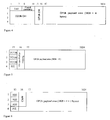
- Figure 1 shows the structure of an OTN frame according to the related art
- Figure 2 shows the principles of 699.84 MHz-based synchronous cross-connect switching according to the related art
- Figure 3 shows a flowchart of the method for synchronous cross-connect switching in optical transport networks according to an embodiment of the present invention
- Figure 4 shows the structure of an ODUs frame according to an embodiment of the present invention
- Figure 5 shows the frame structure of the OPUk portion after an ODUs-Xv frame is split into X ODUs frames according to an embodiment of the present invention
- Figure 6 shows the frame structure of the OPUk portion of an ODUs frame when using an agnostic Constant Bit Rate (CBR) service mapping method according to an embodiment of the present invention
- Figure 7 shows the frame structure of the OPUk portion of an ODUs-Xv frame when using an agnostic Constant Bit Rate (CBR) service mapping method according to an embodiment of the present invention
- Figure 8 shows the principles of synchronous cross-connect performed after OTU signals are demapped into ODU signals according to the an embodiment of the present invention.
- Figure 9 shows the structure of the apparatus for synchronous cross-connect in optical transport networks according to an embodiment of the present invention.
- Optical channel Transport Unit (OTU) signals or Optical Channel Data Unit (ODU) are mapped into interim switching units then are switched by a synchronous cross-connect matrix, so that synchronous hybrid cross-connect of OTN signals at various bit rate levels is performed. Therefore, the switching capacity of the system is expanded.
- OTU signals are the signals with OTU structure, which include OTU1, OTU2, OTU1e/2e, OTU3 and future possible OTU signals defined by ITU-T, for example OTUO, OTU3+ and OTU4.
- ODU signals are the signals with ODU structure, which include ODU1, ODU2, ODU1e/2e, ODU3 and future possible ODU signals defined by ITU-T, for example, ODUO, ODU3e, ODU4e and possible ODU signal carried client signals.
- ODU signals could be obtained by demapping the OTU wrapper or adding ODU wrapper to client signal.
- the bandwidth of interim switching unit which will be described in the embodiments of the present invention is 2.5G b/s rate level.
- the embodiments of the present invention do not try to limit the specified bit rate level for interim switching unit, if the bit rate of the interim switching unit is adopted as other bit rate levels, such as 1.25G b/s, it is still accordant to the range of the present invention.
- the interim switching unit described in the embodiments of the present invention may include the basic interim switching unit and/or the combination of the basic interim switching units.
- the combination of the basic interim switching units is an interim switching unit which combines a number of basic interim switching units via pre-established protocol, and these basic interim switching units are combined in a fixed phase relation, and some additional overhead information should be added to indicate the fixed phase relation.
- the fixed phase relation includes the position of these basic interim switching units, optionally. It is also possible to include the sending order of these basic interim switching units.
- the basic interim switching unit is a signal with fixed structure.
- this kind of basic interim switching unit is called Optical channel data unit switching (ODUs).
- ODUs Optical channel data unit switching
- ODUs-Xv Optical channel data unit switching
- the embodiments of the present invention does not try to limit the interim switching unit as ODUs or ODUs-Xv, it also includes other examples, such as timeslot, in corresponding, the combination of basic interim switching units is timeslot group. And it is easy for this case, so it will not be described in detail.
- One embodiment of the present invention provides a method for synchronous cross-connect switching in optical transport network, which includes:
- Step 11 receiving the OTU signals in the OTN.
- the OTU signals are OTU1 signals.
- Step 12 mapping the OTU1 signal into the ODUs frames that match the bit rates of the OTU1 signals.
- Step 13 performing a synchronous cross-connect switching for the ODUs frames using a synchronous cross-connect matrix.
- Step 14 demapping the ODUs frames after the synchronous cross-connect switching and obtain the OTU1 signals.
- mapping and the demapping may use the same methods described in the other embodiments of the present invention.
- the steps of this embodiment may be implemented by one or more device or units.
- Another embodiment of the present invention provides a method for synchronous cross-connect switching in optical transport network, which includes:
- Step 21 receiving OTU signals in the OTN
- the received OTU signals include at least one of OTU2 and OTU3 signals.
- Step 22 mapping the OTU signals into ODUs-Xv frames that match the bit rates of the OTU signals.
- the ODUs-Xv frames may be obtained by combining a plurality of ODUs frames according to a virtual concatenation rule, and the ODUs-Xv frames have higher capacity than the ODUs frames so that the ODUs-Xv frames can carry the OTU signals having higher bit rates, for example, OTU2 and OTU3 signals.
- Step 23 dividing the ODUs-Xv frames into a plurality of groups having parallel ODUs frames.
- Step 24 performing a synchronous cross-connect switching on the a plurality of groups having parallel ODUs frames.
- Step 25 assembling the parallel ODUs frames belonging to the same group after the synchronous cross-connect switching into the ODUs-Xv frames in step 2.
- Step 26 demapping the ODUs-Xv frames to obtain the OTU signals in the step 1.
- the steps of removing outer encapsulation of the OTU signals and performing an outer encapsulation to the optical channel data units may also be included.
- mapping and the demapping may use the same methods described in the other embodiments of the present invention.
- the steps of this embodiment may be implemented by one or more devices or units.
- one embodiment of the present invention provides a method for synchronous cross-connect switch in optical transport networks.
- a 2.5 Gb/s bit rate level is taken as the switching granularity of ODUs frame and is taken as an example.
- the method includes the following steps.
- step 101 ODUs frames and ODUs virtual concatenation frames are preset.
- the ODUs frames are used to carry OTU1 signal and the ODUs-Xv frames are used to carry OTUk signal having higher bit rate such as OTU2 or OTU3 signal.
- the bit rate of the ODUs frame is slightly higher than the bit rate of OTU1 signal. Therefore, the ODUs frame is able to carry OTU1 signal. Similarly, the rate of the ODUs-Xv frame is higher than all the other OTUk signals except OTU1 signals (k > 1), thus the ODUs-Xv frame is able to carry all the other OTUk signals.
- ODUs-Xv frame may be obtained after virtual concatenation, where X equals 4 or 16; ODUs-4v frame can carry OTU2 signals and ODUs-16v frame can carry OTU3 signals.
- the ODUs frame may adopt the standard ODU frame structure or a simplified ODU frame structure. As shown in Figure 4 , when the OTU OH excluding the FEC OH in a standard ODU frame is changed into a fixed padding field, a simplified ODU frame is obtained.
- the simplified ODU frame includes an FAS, a fixed padding field, an ODUk OH, an OPUk OH, and a payload area.
- the ODUk OH monitors the transport status of the ODUs frame.
- the ODUk OH may be further simplified to provide only an bit error detection function for the ODUs frame so as to reduce the complexity and cost of apparatus.
- Figure 5 shows the frame structure of the OPUk portion after an ODUs-Xv frame is split into X ODUs frames.
- several Virtual Concatenation Overhead (VCOH) bytes replace the reserved bytes in the OPUk OH. These VCOH bytes are used to identify the fixed phase relation among the ODUs frames, that is, the sequence of the ODUs frames.
- the delay between the ODUs frames may be controlled by control the wirings in a circuit board so that the multiframe MFI1/MFI2 function in the VCOH may be omitted and the cache is not needed to align the delay so as to save logical resources.
- step 102 receive OTU signals in an OTN.
- the received OTU signals may be OTU1, OTU2, and/or OTU3 signals of various bit rate levels or at least one of them.
- the OTU signals of each bit rate level may further include multiple channels of OTUk signals. For instance, one channel of OTU1 signals, two channels of OTU2 signals and five channels of OTU3 signals may be received.
- the received signals may also be OTU1e, OTU2e or other similar signals.
- step 103 map the received OTU signals into the ODUs or ODUs-Xv frames that match the bit rate of the received OTU signals.
- OTU1 (2.666057143 Gb/s) ----> ODUs; OTU2 (10.709225316 Gb/s) ----> ODUs-4v; OTU3 (43.018413559 Gb/s) ----> ODUs-16v.
- the reference frequency offset is allowed to be ⁇ 20 ppm or a smaller range.
- an agnostic Constant Bit Rate (CBR) service mapping method may be used to perform asynchronous mapping.
- CBR Constant Bit Rate
- an agnostic CBR mapping method is put forward to flexibly map customer signals.
- the agnostic CBR mapping method suites scenarios where multiple types of OTU signals such as OTU1, OTU2, OTU1e, OTU2e and OTU3 exist and hybrid switching is required.
- Cn which is the number of customer signal bytes to be sent in the next frame is first mapped into a Cbyte field in the overhead area, and then the Cn customer signal bytes are mapped in a distributed way into ODUs or ODUs-Xv frames using a ⁇ - ⁇ algorithm.
- FIG. 6 shows the frame structure of the OPUk portion of an ODUs frame when the agnostic CBR mapping method is applied.
- the OPUk OH includes a Payload Structure Identifier (PSI), a Cbyte field, and some reserved bytes (RES).
- PSI Payload Structure Identifier
- RES reserved bytes
- the PSI identifies the structure type of the OPUk.
- the Cbyte carries the Cn (the number of customer signal bytes to be sent in the next ODUs frame).
- the reserved bytes are reserved for future standardized expansion.
- FIG. 7 shows the structure of the OPUk portion after an ODUs-Xv frame is split when the agnostic CBR mapping method is applied.
- the OPUk OH includes a PSI, a Cbyte field, and several Virtual Concatenation (VCOH) bytes.
- the PSI identifies the structure type of virtual concatenation.
- the Cbyte field carries the Cn (the number of customer signal bytes to be sent in the next ODUs-Xv frame).
- the VCOH bytes indicate the use of virtual concatenation.
- the bit padding method used for mapping can better eliminate the clock jitter caused by padding and improve the quality of the clocks restored at the receiving end.
- bit padding method and the byte padding method, it is necessary to pad a fixed number of bits or bytes in an ODUs or ODUs-Xv frame.
- a certain number of justification bites or bytes must be reserved, similar to the Positive Justification Byte (PJO) or Negative Justification Byte (NJO) defined in ITU-T Recommendation G.709, so as to absorb the asynchronous frequency offset between ODU1/ODU2/ODU3 signals and ODUs/ODUs-4v/ODUs-16v frame signals.
- PJO Positive Justification Byte
- NJO Negative Justification Byte
- OPUk and OPUk-Xv overheads are added in the following way after the mapping is completed:
- a PSI and an OH specified for mapping are added to each of the ODUs or ODUs-Xv frames after the mapping.
- VCOHs are also be added.
- a fixed padding field is added to replace the unused overhead bytes.
- step 104 the ODUs-Xv frames are divided into multiple groups of parallel ODUs frames, and then ODUk OH bytes are added to the ODUs frames divided from the ODUs-Xv frames whereas OTUk OH bytes are added to the ODUs frames that carry OTU1 signals so as to form complete ODUs frame signals:
- the ODUs-Xv frames are divided according to the virtual concatenation rules previously mentioned into multiple groups of parallel ODUs frame signals.
- the ODUs frames that carry OTU1 signals are not divided. For instance, the ODUs frames that carry OTU1 signals are not divided but each channel of ODUs-4v frames carrying OTU2 signals is split into 4 channels of parallel ODUs frame signals whereas each channel of ODUs-16v frames carrying OTU3 signals is split into 16 channels of parallel ODUs frame signals.
- the 4 channels of ODUs frame signals are organized into a group to carry complete OTU2 signals.
- the 16 channels of ODUs frame signals are organized into a group to carry complete OTU3 signals.
- the added OH bytes include FAS, OTUk OH (excluding FEC) and ODUk OH bytes.
- a fixed padding field is also added to replace the unused OTUk OH (excluding FEC) and the unused ODUk OH.
- the signals are scrambled to form complete ODUs frame signals.
- step 105 the synchronous cross-connect matrix performs synchronous cross-connect switching for the complete ODUs frame signals.
- the synchronous cross-connect matrix may assume one of multiple forms.
- the synchronous cross-connect matrix may be an N ⁇ N CLOS cross-connect network, that is, a common 3-layer CLOS cross-connect network or a bit slice cross-connect network or other similar ones.
- step 106 the ODUs frame signals obtained after the switching by the synchronous cross-connect matrix are interpreted.
- the groups of parallel ODUs frames after the above-mentioned bound switching are assembled into ODUs-Xv frames.
- step 104 If scrambling is applied in step 104, then the ODUs frame signals are descrambled before they are interpreted.
- the step for interpreting the ODUs frame signals further includes interpreting the FAS OH, OTUk OH, ODUk OH and OPUk OH of each ODUs frame, and detecting the errors of ODUs frames.
- the fixed padding portion is omitted.
- For a group of parallel ODUs frame signals after the bound switching first all the parallel ODUs frames in the group are aligned according to the frame alignment signal in the FAS OH and then are assembled into ODUs-Xv frames according to the VCOHs in the OPUk OH.
- step 107 the ODUs frames that do not belong to any group after the interpretation and the ODUs-Xv frames after the assembly are de-mapped to restore the received OTU signals previously mentioned.
- the above-mentioned demapping refers to demapping the frames using the previously-mentioned bit padding, byte padding or agnostic CBR mapping method as indicated by the PSI to restore the received OTU signals and then sending the OTU signals.
- a 2.5 Gb/s bit rate is used for switching ODUs frames.
- the bit rate level of ODUs frames may be chosen according to the actual backplane bit rate maturity. For instance, when the received OTU signals include multiple channels of OTU1 signals, a 5 Gb/s or 10 Gb/s bit rate may be set for the ODUs frames and then the bit rate level of the ODUs frames is higher than the bit rate level of the OTU1 signals and thus the bit slice method may be adopted to map the received OTU1 signals into ODUs frames for cross-connect switching.
- the outer encapsulation of the received OTU signals may further be removed to obtain ODU signals.
- bit rate adaptation is performed for the ODU signals to map the ODU signals into the preset ODUs or ODUs-Xv frames. Accordingly, the ODUs or ODUs-Xv frames after synchronous cross-connect switching are demapped into the ODU signals and then outer encapsulation is performed to form the above-mentioned OTU signals.
- the ODU signals are mapped into ODUs or ODUs-Xv frames and a relationship may apply during the demapping of these ODUs or ODUs-Xv frames: ODU1 (2.498775126 Gb/s) ----> ODUs; ODU2 (10.037273924 Gb/s) ----> ODUs-4; ODU3 (40.319218983 Gb/s) ----> ODUs-16v.
- ODU1 (2.498775126 Gb/s)
- ODU2 (10.037273924 Gb/s)
- ODU3 (40.319218983 Gb/s)
- the reference frequency offset is allowed to be ⁇ 20 ppm or a smaller range.
- the reference frequency of the ODUs frame signals may slightly deviate from the above-calculated value.
- OTU signals are mapped into the preset ODUs or ODUs-Xv frames, which are then switched using a synchronous cross-connect matrix to complete synchronous hybrid cross-connect switching of OTN signals at various bit rate levels, so as to improve the compatibility of the switching technology and reduce the development cost of chips.
- the ODUs frames may use an appropriate bit rate to effectively lower the requirements on logical resources. For instance, a 2.5 GHz bit rate level can reduce the consumed logical resources and effectively save power consumption and cost.
- the N ⁇ N CLOS network or bit slice cross-connect network used for synchronous cross-connect switching can further expand the switching capacity of the system, solve the capacity limitation that exists with asynchronous cross-connect switching, maximally improve the switching capacity of the system, and effectively bring into play the advantages of large-granularity cross-connect switching in OTN. Furthermore, as ODUs frames are compatible with OTN frames, the development workload of cross-connect chips is reduced and the system implementation is quicker. With the use of the agnostic CBR mapping method during asynchronous mapping, the mapping paths of various ODUk signals are unified. This improves the reuse of chip codes and reduces the cost of chip research and development.
- the apparatus for synchronous cross-connect switching in optical transport networks includes the following modules:
- a receiving module which receives Optical Transport Unit (OTU) signals in an Optical Transport Network (OTN);
- OFT Optical Transport Unit
- a mapping and dividing module which maps the OTU signals received by the receiving module into ODUs or ODUs-Xv frames, and divides the ODUs-Xv frames into multiple groups of parallel ODUs frames;
- a switching module which performs synchronous cross-connect switching for the ODUs frames obtained by the mapping and dividing module using a synchronous cross-connect matrix
- An assembly and demapping module which assembles the groups of parallel ODUs frames obtained by the switching module into ODUs-Xv frames, and demaps the ODUs-Xv frames that are obtained after the assembly and the ODUs frames that do not belong to any group among the ODUs frames obtained by the switching module into OTU signals.
- mapping and dividing module may further include the following units:
- a decapsulation unit which removes the outer encapsulation of the OTU signals received by the receiving module to obtain ODU signals
- a mapping unit which maps the ODU signals obtained by the decapsulation unit into ODUs frames or ODUs-Xv frames;
- a dividing unit which divides the ODUs-Xv frames obtained by the mapping unit into multiple groups of parallel ODUs frames
- the assembly and demapping module may also further include the following units:
- An assembly unit which assembles the groups of ODUs frames obtained by the switching module into the above-mentioned ODUs-Xv frames;
- a demapping unit which demaps the ODUs-Xv frames obtained by the assembly unit and the ODUs frames that do not belong to any group among the ODUs frames obtained by the switching module into ODU signals;
- An encapsulation unit which performs an outer encapsulation to the ODU signals obtained by the demapping unit into OTU signals.
- the ODUs frames carry OTU1 signals whereas the ODUs-Vx frames carry the other OTU signals.
- the mapping and dividing module maps OTU signals into the preset ODUs or ODUs-Xv frames and then the switching module switches the ODUs or ODUs-Xv frames using a synchronous cross-connect matrix to complete synchronous hybrid cross-connect switching of OTN signals at various bit rate levels, so as to improve the compatibility of the switching technology and reduce the development cost of chips.
- the ODUs frames may use an appropriate bit rate to effectively lower the requirements on logical resources.
- the N ⁇ N CLOS network or bit slice cross-connect network used for synchronous cross-connect switching can further expand the switching capacity of the system, solve the capacity limitation that exists with asynchronous cross-connect switching, maximally improve the switching capacity of the system, and effectively bring into play the advantages of large-granularity cross-connect switching in OTN. Furthermore, as ODUs frames are compatible with OTN frames, the development workload of cross-connect chips is reduced and the system implementation is quicker. With the use of the agnostic CBR mapping method during asynchronous mapping, the mapping paths of various ODUk signals are unified. This improves the reuse of chip codes and reduces the cost of chip research and development.
- One embodiment of the present invention provides a network apparatus that may be used in theoptical transport network, the network apparatus includes a receiving unit, a mapping unit, a synchronous cross-connect matrix and a demapping unit.
- the receiving unit is configured to receive the OTU signals in the OTN
- the mapping unit is configured to mapping the received OTU signals into interim switching units
- the synchronous cross-connect matrix is configured to perform a synchronous cross-connect switching for the interim switching units
- the demapping unit is configured to demap the interim switching units after the synchronous cross-connect switching to obtain the OTU signals.
- the interim switching units can carry the OTU signals, and match the bit rates of the OTU signals.
- the bit rate of the interim switching units is slightly higher than that of the OTU signals so the interim switching units can carry the OTU signals.
- the interim switching units may include optical channel data unit switching frames (ODUs frames) and optical channel data unit switching virtual concatenation frames (ODUs-Xv), the ODUs frames carry the OTU1 signals and the ODUs-Xv carry the OTU signals having higher bit rates than the OTU1 signals, for example, OTU2 and/or OTU3 signals.
- the interim switching units may be obtained by preset.
- the network apparatus may further include decapsulation unit configured to remove the outer encapsulation of the received OTU signals to obtain the optical channel data units, and a encapsulating unit to perform an outer encapsulation to the optical channel data unit obtained demapping the interim switching units.
- Various embodiments of the present invention may be embodied via software.
- the programs of the software may be stored in an accessible storage media such as the hard disk or cache of a network apparatus in the optical transport network.
Claims (17)
- Une méthode pour une commutation répartitrice synchronisée sur un réseau de transport optique, comprenant :la réception de signaux d'une unité de données de canal optique, UDO, (102) ;
caractérisée par le mappage des signaux UDO dans des unités intermédiaires (103), où les unités intermédiaires de commutation adoptent une structure cadre des signaux UDO, ou une structure cadre obtenue en procédant à un remplissage fixe vers plusieurs surdébits des signaux UDO, et qui correspond au débit binaire des signaux UDO reçus ;exécution d'une commutation répartitrice synchronisée sur la base des unités intermédiaires de commutation (105) ; etdémappage des unités intermédiaires de commutation obtenues après la commutation répartitrice synchronisée pour obtenir les signaux UDO (107). - La méthode de la revendication 1, mappage des signaux UDO dans les unités intermédiaires de commutation via un débit binaire constant, DBC, agnostique, une méthode de mappage du service, une méthode de remplissage d'octets, ou une méthode de remplissage de bits.
- La méthode de la revendication 1, où le débit binaire des unités intermédiaires de commutation est supérieur à celui des signaux UDO.
- La méthode de la revendication 1, où les signaux UDO ont un faible débit binaire, les unités intermédiaires de commutation sont des commutations d'unités de données optiques (UDO).
- La méthode de la revendication 1, comprenant de plus les étapes de :mappage des signaux UDO dans des cadres virtuels de concaténation des commutations d'unités de données de canal optique (UDO-Xv), où les cadres UDO-Xv sont obtenus en combinant une pluralité de cadres UDO, conformément à une règle préétablie ;répartition des cadres UDO-Xv en une pluralité de groupes ayant des cadres UDO parallèles ;exécution de la commutation répartitrice synchronisée pour la pluralité de groupes ayant des cadres UDO parallèles ;assemblage des cadres UDO parallèles appartenant à un même groupe dans les cadres UDO-Xv ; etdémappage des cadres UDO-Xv pour obtenir les signaux UDO.
- La méthode de la revendication 1, où les signaux UDO reçus comprennent les premiers signaux UDO et les seconds signaux UDO, et la méthode comprend de plus les étapes de :mappage des premiers signaux UDO dans des cadres UDO, et mappage des seconds signaux UDO dans des cadres UDO-Xv, où les cadres UDO-Xv sont obtenus en combinant une pluralité de cadres UDO, conformément à une règle préétablie ;répartition des cadres UDO-Xv en une pluralité de groupes ayant des cadres UDO parallèles, conformément à la règle actuelle ;exécution de la commutation répartitrice synchronisée pour la pluralité de groupes ayant des cadres UDO parallèles et des cadres UDO où les premiers signaux UDO sont mappés ;assemblage des cadres UDO parallèles appartenant à un même groupe dans les cadres UDO-Xv ; etdémappage des cadres UDO-Xv et des cadres UDO où les premiers signaux UTO sont mappés pour obtenir des signaux UDO.
- La méthode de la revendication 5 ou de la revendication 6, où les cadres UDO-XV sont obtenus en combinant la pluralité d'UDO, conformément à une relation de phase fixe.
- La méthode de la revendication 7, où la relation de phase fixe comprend une position de pluralité de cadres UDO, ou un ordre d'envoi de la pluralité de cadres UDO.
- La méthode de la revendication 5 ou de la revendication 6, où la règle actuelle est une règle de concaténation virtuelle.
- Un équipement de réseau comprenant :une unité réceptrice, configurée pour recevoir des signaux UDO ;caractérisée par une unité de mappage, configurée pour mapper les signaux UDO en des unités intermédiaires de commutation, où les unités intermédiaires de commutation correspondent aux débits binaires des signaux UDO, et qui sont configurées pour transporter les signaux UTO ;une matrice répartitrice synchronisée, configurée pour exécuter une commutation de matrice répartitrice synchronisée pour les unités intermédiaires de commutation ; etune unité de démappage, configurée pour démapper les unités intermédiaires de commutation afin d'obtenir les signaux UDO.
- L'équipement de réseau de la revendication 10, où les signaux UDO sont des signaux UTO1, les unités intermédiaires de commutation sont des cadres UDO.
- L'équipement de réseau de la revendication 10, où les signaux UDO sont des signaux UTO2 ou UTO3, les unités intermédiaires de commutation sont des cadres UDO, les cadres UDO-Xv sont obtenus en combinant une pluralité de cadres UDO, conformément à une règle préétablie, l'équipement de réseau comprend de plus :une unité de répartition, configurée pour répartir des cadres UDO-Xv en une pluralité de groupes ayant des cadres UDO parallèles ;une unité d'assemblage, configurée pour assembler des cadres UDO parallèles appartenant à un même groupe dans les cadres UDO-Xv.
- L'équipement de réseau de la revendication 12, où la règle actuelle est une relation fixe.
- L'équipement de réseau de la revendication 12, où la relation de phase fixe est une position de la pluralité d'UDO, ou un ordre d'envoi de la pluralité d'UDO.
- L'équipement de réseau de la revendication 10, où :les signaux UDO reçus comprennent les premiers signaux UDO et les seconds signaux UDO;l'unité de mappage est de plus configurée pour mapper les premiers signaux UDO dans des cadres UDO, et pour mapper les seconds signaux UDO dans des cadres UDO-Xv, et répartir les cadres UDO-Xv en une pluralité de groupes ayant des cadres UDO parallèles, où les cadres UDO-Xv sont obtenus en combinant une pluralité de cadres UDO, conformément à une règle préétablie ; etl'équipement de réseau comprend de plus :un module de commutation, configuré pour exécuter une commutation répartitrice synchronisée pour les cadres UDO et la pluralité de groupes ayant des cadres UDO parallèles en utilisant une matrice répartitrice synchronisée ; etun module d'assemblage et de démappage, configuré pour assembler les cadres UDO parallèles appartenant à un même groupe dans les cadres UDO-Xv, et démapper les cadres UDO-Xv et les cadres UDO pour obtenir les premiers signaux UDO et les seconds signaux UDO.
- L'équipement de réseau de la revendication 15, où les premiers signaux UDO ont un faible débit binaire, et où les seconds signaux UDO ont un débit binaire élevé.
- Un dispositif lisible par ordinateur, comprenant une logique codifiée dans le dispositif lisible par ordinateur, la logique - quand exécutée par un ordinateur - étant configurée pour que l'ordinateur exécute toutes les étapes de la revendication 1.
Applications Claiming Priority (1)
| Application Number | Priority Date | Filing Date | Title |
|---|---|---|---|
| CN2007101217415A CN101389146B (zh) | 2007-09-13 | 2007-09-13 | 光传送网同步交叉调度的方法和装置 |
Publications (2)
| Publication Number | Publication Date |
|---|---|
| EP2037604A1 EP2037604A1 (fr) | 2009-03-18 |
| EP2037604B1 true EP2037604B1 (fr) | 2009-11-04 |
Family
ID=40043036
Family Applications (1)
| Application Number | Title | Priority Date | Filing Date |
|---|---|---|---|
| EP08164221A Active EP2037604B1 (fr) | 2007-09-13 | 2008-09-12 | Procédé et appareil pour commutation de répartiteur synchrone dans un réseau de transport optique |
Country Status (5)
| Country | Link |
|---|---|
| US (1) | US7782843B2 (fr) |
| EP (1) | EP2037604B1 (fr) |
| CN (1) | CN101389146B (fr) |
| AT (1) | ATE447804T1 (fr) |
| DE (1) | DE602008000260D1 (fr) |
Families Citing this family (42)
| Publication number | Priority date | Publication date | Assignee | Title |
|---|---|---|---|---|
| EP2192787B1 (fr) * | 2008-11-28 | 2011-01-26 | Alcatel Lucent | Procédé et appareil de protection d'équipement |
| US8359525B2 (en) * | 2009-03-06 | 2013-01-22 | Electronics And Telecommunications Research Institute | Method and apparatus for transmitting data in optical transport network |
| CN101834688B (zh) * | 2009-03-09 | 2011-08-31 | 华为技术有限公司 | 光传送网中的映射、解映射方法及装置 |
| CN102017521B (zh) * | 2009-06-04 | 2012-09-05 | 华为技术有限公司 | 实现光信道数据单元共享保护环的方法和装置 |
| US20120148240A1 (en) * | 2009-06-26 | 2012-06-14 | Telefonaktiebolaget L M Ericsson (Publ) | Reserving a path using gmpls extensions for odu signalling |
| CN101610430B (zh) * | 2009-06-30 | 2013-03-27 | 中兴通讯股份有限公司 | 一种实现ODUk交叉调度的方法和装置 |
| US8446906B2 (en) | 2009-07-01 | 2013-05-21 | Infinera Corporation | Providing access to client overhead while transparently transmitting the client signal |
| CN101616341B (zh) * | 2009-08-05 | 2012-10-10 | 中兴通讯股份有限公司 | 一种交叉保护的方法和装置 |
| CN101998184B (zh) * | 2009-08-12 | 2015-04-01 | 中兴通讯股份有限公司 | 适配装置及方法 |
| CN101998182B (zh) * | 2009-08-25 | 2013-08-14 | 华为技术有限公司 | 光网络中的信息处理方法、光通信装置和光通信系统 |
| CN101702637B (zh) * | 2009-10-30 | 2015-01-28 | 中兴通讯股份有限公司 | 时隙交叉方法和系统 |
| EP2532106B1 (fr) * | 2010-02-02 | 2020-04-08 | Telefonaktiebolaget LM Ericsson (publ) | Différenciation de trafic dans un réseau de transport |
| CN101814968B (zh) * | 2010-03-16 | 2014-06-11 | 中兴通讯股份有限公司 | 实现帧头对齐和复帧归零的方法及装置 |
| CN102201973B (zh) * | 2010-03-25 | 2015-08-12 | 中兴通讯股份有限公司 | 一种基于g.709的多级复用路由控制方法和网关网元 |
| JP5344088B2 (ja) * | 2010-04-30 | 2013-11-20 | 富士通株式会社 | データ量導出装置 |
| GB2495673A (en) * | 2010-07-30 | 2013-04-17 | Fujitsu Ltd | Signal storage method, frame generating device, frame receiving device and transmission system |
| CN102572618B (zh) * | 2010-12-17 | 2015-09-16 | 中兴通讯股份有限公司 | 一种基于g.709的多级复用路由控制方法和网关网元 |
| CN102594648B (zh) * | 2011-01-07 | 2014-11-05 | 中兴通讯股份有限公司 | 业务调度方法及装置 |
| CN102655470B (zh) * | 2011-03-02 | 2015-08-12 | 中兴通讯股份有限公司 | 在光传送网中节点实现业务调度的方法和系统 |
| JP5736964B2 (ja) * | 2011-05-26 | 2015-06-17 | 富士通株式会社 | 伝送装置及びデータ伝送方法 |
| US8934479B2 (en) * | 2011-10-28 | 2015-01-13 | Infinera Corporation | Super optical channel transport unit signal supported by multiple wavelengths |
| CN104365114A (zh) * | 2012-04-04 | 2015-02-18 | 瑞典爱立信有限公司 | 用于使用分级数据结构交换传输的信息的装置和方法 |
| US9167272B2 (en) * | 2012-04-25 | 2015-10-20 | Omnivision Technologies, Inc. | Method, apparatus and system for exchanging video data in parallel |
| CN103384178B (zh) * | 2012-05-02 | 2017-10-17 | 中兴通讯股份有限公司 | 类odu帧的映射方法及装置 |
| CN106301661B (zh) * | 2012-07-30 | 2018-10-19 | 华为技术有限公司 | 光传送网中传送、接收客户信号的方法和装置 |
| US9288006B1 (en) | 2012-09-21 | 2016-03-15 | Pmc-Sierra Us, Inc. | Demultiplexing high-order to low-order ODU signals in an optical transport network |
| EP2738964A1 (fr) * | 2012-12-03 | 2014-06-04 | Alcatel Lucent | Procédé et appareil pour transmettre un signal de transport asynchrone sur une section optique |
| ES2640440T3 (es) * | 2012-12-05 | 2017-11-03 | Huawei Technologies Co., Ltd. | Procedimiento de procesamiento de datos, placa única de comunicación y dispositivo |
| ES2629184T3 (es) | 2013-03-15 | 2017-08-07 | Huawei Technologies Co., Ltd. | Dispositivo y método de transferencia de servicio para unidad de datos de canal óptico |
| US9438376B2 (en) * | 2013-03-15 | 2016-09-06 | Cortina Systems, Inc. | Apparatus and method for forward error correction over a communication channel |
| WO2014139180A1 (fr) | 2013-03-15 | 2014-09-18 | 华为技术有限公司 | Dispositif et procédé de transfert de service d'unité de données de canal optique (odu) |
| US8958514B2 (en) * | 2013-07-12 | 2015-02-17 | IPLight Ltd. | Clock recovery in communication of hierarchically encapsulated signals |
| CN103840878B (zh) * | 2014-02-26 | 2016-04-13 | 烽火通信科技股份有限公司 | Otn设备基于odu0/1颗粒的电交叉容量测试系统及方法 |
| EP2916561B1 (fr) * | 2014-03-05 | 2016-06-22 | Alcatel Lucent | Commutateur crossbar pour un réseau WDM |
| US10079641B1 (en) * | 2014-04-01 | 2018-09-18 | Sprint Spectrum, L.P. | Systems and methods of transporting data over an optical transport network |
| CN105790875B (zh) * | 2014-12-24 | 2019-04-30 | 深圳市中兴微电子技术有限公司 | 一种交叉调度方法及其装置 |
| CN106559141B (zh) | 2015-09-25 | 2020-01-10 | 华为技术有限公司 | 一种信号发送、接收方法、装置及系统 |
| CN106982105B (zh) * | 2016-01-15 | 2020-03-31 | 华为技术有限公司 | 处理弹性以太网信号的方法和装置 |
| US10298348B2 (en) | 2016-04-01 | 2019-05-21 | Ipg Photonics Corporation | Transparent clocking in a cross connect system |
| CN109412746B (zh) | 2017-08-15 | 2021-01-05 | 深圳市海思半导体有限公司 | 数据处理的方法和相关装置 |
| CN113411689B (zh) * | 2020-03-17 | 2023-04-11 | 华为技术有限公司 | 一种数据帧的传送方法以及相关设备 |
| CN114466087B (zh) * | 2022-02-21 | 2023-05-30 | 重庆奥普泰通信技术有限公司 | 数据传输方法、装置、设备以及存储介质 |
Family Cites Families (15)
| Publication number | Priority date | Publication date | Assignee | Title |
|---|---|---|---|---|
| US6430201B1 (en) * | 1999-12-21 | 2002-08-06 | Sycamore Networks, Inc. | Method and apparatus for transporting gigabit ethernet and fiber channel signals in wavelength-division multiplexed systems |
| EP1229692A1 (fr) * | 2001-02-02 | 2002-08-07 | BRITISH TELECOMMUNICATIONS public limited company | Procédé et dispositif pour un mode tunnel dans un réseau |
| JP3586204B2 (ja) * | 2001-02-19 | 2004-11-10 | 日本電信電話株式会社 | 多重化中継伝送装置 |
| ATE281746T1 (de) * | 2001-07-23 | 2004-11-15 | Cit Alcatel | Netzelement für signale des optical transport networks (otn) |
| US20030048813A1 (en) * | 2001-09-05 | 2003-03-13 | Optix Networks Inc. | Method for mapping and multiplexing constant bit rate signals into an optical transport network frame |
| US7286487B2 (en) * | 2002-11-18 | 2007-10-23 | Infinera Corporation | Optical transmission network with asynchronous mapping and demapping and digital wrapper frame for the same |
| US7787460B2 (en) * | 2003-10-08 | 2010-08-31 | Ciena Corporation | System and method for switching packet traffic over an optical transport network |
| DE602004012066T2 (de) * | 2004-04-05 | 2009-03-19 | Alcatel Lucent | Zeitmultiplexstreckenverbindungen zwischen einer Koppelmatrix und einem Port in einem Netzelement |
| CN1791278B (zh) * | 2004-12-14 | 2010-04-14 | 华为技术有限公司 | 光传送网络调度系统及其方法 |
| CN100584103C (zh) * | 2005-03-10 | 2010-01-20 | 华为技术有限公司 | 光传送网中的信号调度方法和系统 |
| US7711007B2 (en) | 2005-04-28 | 2010-05-04 | Alcatel-Lucent Usa Inc. | Method and apparatus for synchronous switching of optical transport network signals |
| US8908674B2 (en) * | 2005-08-08 | 2014-12-09 | Telecom Italia S.P.A. | Method for configuring an optical network |
| US8699886B2 (en) * | 2005-11-23 | 2014-04-15 | Ciena Corporation | Externally synchronized optical transport network systems and associated methods |
| CN101159495B (zh) * | 2006-10-08 | 2012-07-04 | 华为技术有限公司 | 无源光纤网络中信号传送系统、设备及方法 |
| US8054853B2 (en) * | 2007-01-29 | 2011-11-08 | Ciena Corporation | Systems and methods for combining time division multiplexed and packet connection in a meshed switching architecture |
-
2007
- 2007-09-13 CN CN2007101217415A patent/CN101389146B/zh active Active
-
2008
- 2008-09-12 EP EP08164221A patent/EP2037604B1/fr active Active
- 2008-09-12 US US12/209,619 patent/US7782843B2/en active Active
- 2008-09-12 DE DE602008000260T patent/DE602008000260D1/de active Active
- 2008-09-12 AT AT08164221T patent/ATE447804T1/de not_active IP Right Cessation
Also Published As
| Publication number | Publication date |
|---|---|
| US7782843B2 (en) | 2010-08-24 |
| EP2037604A1 (fr) | 2009-03-18 |
| DE602008000260D1 (de) | 2009-12-17 |
| US20090074410A1 (en) | 2009-03-19 |
| CN101389146B (zh) | 2011-01-05 |
| ATE447804T1 (de) | 2009-11-15 |
| CN101389146A (zh) | 2009-03-18 |
Similar Documents
| Publication | Publication Date | Title |
|---|---|---|
| EP2037604B1 (fr) | Procédé et appareil pour commutation de répartiteur synchrone dans un réseau de transport optique | |
| EP3462647B1 (fr) | Procédé de transport d'un signal de client dans un réseau de transport optique, et dispositif de transport | |
| EP2107705B1 (fr) | Procédé de multiplexage de données ethernet indépendantes, dispositif et système associés | |
| EP1826925B1 (fr) | Systeme de programmation uniforme de reseau optique synchrone et de reseau de transport optique, et procede | |
| EP2120380B1 (fr) | Procédé de multiplexage et de démultiplexage de service de faible débit binaire | |
| US8374186B2 (en) | Method, apparatus and system for transmitting and receiving client signals | |
| EP1826926B1 (fr) | Procede de transmission de signal de trafic bas debit dans un reseau de transport optique | |
| US9497064B2 (en) | Method and apparatus for transporting ultra-high-speed Ethernet service | |
| US11405703B2 (en) | Method and apparatus for transmission using interface, and device | |
| WO2006051041A1 (fr) | Procede et appareil permettant de transporter un signal de couche client sur un reseau de transport optique (otn) | |
| CN113395613B (zh) | 一种业务承载的方法、装置和系统 | |
| US8238365B2 (en) | Method and device for supporting optical transmission network service dispatch in optical synchronization network | |
| US11910135B2 (en) | Optical signal transmission method and related apparatus | |
| US7711007B2 (en) | Method and apparatus for synchronous switching of optical transport network signals | |
| CN101150879B (zh) | 基于光传送网的交叉调度系统和方法 | |
| CN101350691B (zh) | 一种业务汇聚和adm分插复用方法及设备 | |
| KR20090039403A (ko) | 종속신호를 통합하는 방법 및 통합 접속보드 |
Legal Events
| Date | Code | Title | Description |
|---|---|---|---|
| PUAI | Public reference made under article 153(3) epc to a published international application that has entered the european phase |
Free format text: ORIGINAL CODE: 0009012 |
|
| AK | Designated contracting states |
Kind code of ref document: A1 Designated state(s): AT BE BG CH CY CZ DE DK EE ES FI FR GB GR HR HU IE IS IT LI LT LU LV MC MT NL NO PL PT RO SE SI SK TR |
|
| AX | Request for extension of the european patent |
Extension state: AL BA MK RS |
|
| 17P | Request for examination filed |
Effective date: 20090512 |
|
| GRAP | Despatch of communication of intention to grant a patent |
Free format text: ORIGINAL CODE: EPIDOSNIGR1 |
|
| RIN1 | Information on inventor provided before grant (corrected) |
Inventor name: WU, QIUYOU Inventor name: DONG, LIMIN Inventor name: ZOU, SHIMIN |
|
| GRAS | Grant fee paid |
Free format text: ORIGINAL CODE: EPIDOSNIGR3 |
|
| GRAA | (expected) grant |
Free format text: ORIGINAL CODE: 0009210 |
|
| AK | Designated contracting states |
Kind code of ref document: B1 Designated state(s): AT BE BG CH CY CZ DE DK EE ES FI FR GB GR HR HU IE IS IT LI LT LU LV MC MT NL NO PL PT RO SE SI SK TR |
|
| REG | Reference to a national code |
Ref country code: GB Ref legal event code: FG4D |
|
| REG | Reference to a national code |
Ref country code: CH Ref legal event code: EP |
|
| AKX | Designation fees paid |
Designated state(s): AT BE BG CH CY CZ DE DK EE ES FI FR GB GR HR HU IE IS IT LI LT LU LV MC MT NL NO PL PT RO SE SI SK TR |
|
| REG | Reference to a national code |
Ref country code: IE Ref legal event code: FG4D |
|
| REF | Corresponds to: |
Ref document number: 602008000260 Country of ref document: DE Date of ref document: 20091217 Kind code of ref document: P |
|
| LTIE | Lt: invalidation of european patent or patent extension |
Effective date: 20091104 |
|
| PG25 | Lapsed in a contracting state [announced via postgrant information from national office to epo] |
Ref country code: ES Free format text: LAPSE BECAUSE OF FAILURE TO SUBMIT A TRANSLATION OF THE DESCRIPTION OR TO PAY THE FEE WITHIN THE PRESCRIBED TIME-LIMIT Effective date: 20100215 Ref country code: LT Free format text: LAPSE BECAUSE OF FAILURE TO SUBMIT A TRANSLATION OF THE DESCRIPTION OR TO PAY THE FEE WITHIN THE PRESCRIBED TIME-LIMIT Effective date: 20091104 Ref country code: FI Free format text: LAPSE BECAUSE OF FAILURE TO SUBMIT A TRANSLATION OF THE DESCRIPTION OR TO PAY THE FEE WITHIN THE PRESCRIBED TIME-LIMIT Effective date: 20091104 Ref country code: NO Free format text: LAPSE BECAUSE OF FAILURE TO SUBMIT A TRANSLATION OF THE DESCRIPTION OR TO PAY THE FEE WITHIN THE PRESCRIBED TIME-LIMIT Effective date: 20100204 Ref country code: IS Free format text: LAPSE BECAUSE OF FAILURE TO SUBMIT A TRANSLATION OF THE DESCRIPTION OR TO PAY THE FEE WITHIN THE PRESCRIBED TIME-LIMIT Effective date: 20100304 Ref country code: SE Free format text: LAPSE BECAUSE OF FAILURE TO SUBMIT A TRANSLATION OF THE DESCRIPTION OR TO PAY THE FEE WITHIN THE PRESCRIBED TIME-LIMIT Effective date: 20091104 |
|
| PG25 | Lapsed in a contracting state [announced via postgrant information from national office to epo] |
Ref country code: HR Free format text: LAPSE BECAUSE OF FAILURE TO SUBMIT A TRANSLATION OF THE DESCRIPTION OR TO PAY THE FEE WITHIN THE PRESCRIBED TIME-LIMIT Effective date: 20091104 Ref country code: SI Free format text: LAPSE BECAUSE OF FAILURE TO SUBMIT A TRANSLATION OF THE DESCRIPTION OR TO PAY THE FEE WITHIN THE PRESCRIBED TIME-LIMIT Effective date: 20091104 Ref country code: PL Free format text: LAPSE BECAUSE OF FAILURE TO SUBMIT A TRANSLATION OF THE DESCRIPTION OR TO PAY THE FEE WITHIN THE PRESCRIBED TIME-LIMIT Effective date: 20091104 Ref country code: LV Free format text: LAPSE BECAUSE OF FAILURE TO SUBMIT A TRANSLATION OF THE DESCRIPTION OR TO PAY THE FEE WITHIN THE PRESCRIBED TIME-LIMIT Effective date: 20091104 Ref country code: CY Free format text: LAPSE BECAUSE OF FAILURE TO SUBMIT A TRANSLATION OF THE DESCRIPTION OR TO PAY THE FEE WITHIN THE PRESCRIBED TIME-LIMIT Effective date: 20091104 |
|
| PG25 | Lapsed in a contracting state [announced via postgrant information from national office to epo] |
Ref country code: AT Free format text: LAPSE BECAUSE OF FAILURE TO SUBMIT A TRANSLATION OF THE DESCRIPTION OR TO PAY THE FEE WITHIN THE PRESCRIBED TIME-LIMIT Effective date: 20091104 |
|
| PG25 | Lapsed in a contracting state [announced via postgrant information from national office to epo] |
Ref country code: BG Free format text: LAPSE BECAUSE OF FAILURE TO SUBMIT A TRANSLATION OF THE DESCRIPTION OR TO PAY THE FEE WITHIN THE PRESCRIBED TIME-LIMIT Effective date: 20100204 Ref country code: RO Free format text: LAPSE BECAUSE OF FAILURE TO SUBMIT A TRANSLATION OF THE DESCRIPTION OR TO PAY THE FEE WITHIN THE PRESCRIBED TIME-LIMIT Effective date: 20091104 Ref country code: DK Free format text: LAPSE BECAUSE OF FAILURE TO SUBMIT A TRANSLATION OF THE DESCRIPTION OR TO PAY THE FEE WITHIN THE PRESCRIBED TIME-LIMIT Effective date: 20091104 Ref country code: EE Free format text: LAPSE BECAUSE OF FAILURE TO SUBMIT A TRANSLATION OF THE DESCRIPTION OR TO PAY THE FEE WITHIN THE PRESCRIBED TIME-LIMIT Effective date: 20091104 |
|
| PG25 | Lapsed in a contracting state [announced via postgrant information from national office to epo] |
Ref country code: CZ Free format text: LAPSE BECAUSE OF FAILURE TO SUBMIT A TRANSLATION OF THE DESCRIPTION OR TO PAY THE FEE WITHIN THE PRESCRIBED TIME-LIMIT Effective date: 20091104 Ref country code: SK Free format text: LAPSE BECAUSE OF FAILURE TO SUBMIT A TRANSLATION OF THE DESCRIPTION OR TO PAY THE FEE WITHIN THE PRESCRIBED TIME-LIMIT Effective date: 20091104 |
|
| PLBE | No opposition filed within time limit |
Free format text: ORIGINAL CODE: 0009261 |
|
| STAA | Information on the status of an ep patent application or granted ep patent |
Free format text: STATUS: NO OPPOSITION FILED WITHIN TIME LIMIT |
|
| 26N | No opposition filed |
Effective date: 20100805 |
|
| PG25 | Lapsed in a contracting state [announced via postgrant information from national office to epo] |
Ref country code: GR Free format text: LAPSE BECAUSE OF FAILURE TO SUBMIT A TRANSLATION OF THE DESCRIPTION OR TO PAY THE FEE WITHIN THE PRESCRIBED TIME-LIMIT Effective date: 20100205 |
|
| PG25 | Lapsed in a contracting state [announced via postgrant information from national office to epo] |
Ref country code: MC Free format text: LAPSE BECAUSE OF NON-PAYMENT OF DUE FEES Effective date: 20100930 |
|
| PG25 | Lapsed in a contracting state [announced via postgrant information from national office to epo] |
Ref country code: IE Free format text: LAPSE BECAUSE OF NON-PAYMENT OF DUE FEES Effective date: 20100912 |
|
| PG25 | Lapsed in a contracting state [announced via postgrant information from national office to epo] |
Ref country code: MT Free format text: LAPSE BECAUSE OF FAILURE TO SUBMIT A TRANSLATION OF THE DESCRIPTION OR TO PAY THE FEE WITHIN THE PRESCRIBED TIME-LIMIT Effective date: 20091104 |
|
| PG25 | Lapsed in a contracting state [announced via postgrant information from national office to epo] |
Ref country code: LU Free format text: LAPSE BECAUSE OF NON-PAYMENT OF DUE FEES Effective date: 20100912 Ref country code: HU Free format text: LAPSE BECAUSE OF FAILURE TO SUBMIT A TRANSLATION OF THE DESCRIPTION OR TO PAY THE FEE WITHIN THE PRESCRIBED TIME-LIMIT Effective date: 20100505 |
|
| PG25 | Lapsed in a contracting state [announced via postgrant information from national office to epo] |
Ref country code: TR Free format text: LAPSE BECAUSE OF FAILURE TO SUBMIT A TRANSLATION OF THE DESCRIPTION OR TO PAY THE FEE WITHIN THE PRESCRIBED TIME-LIMIT Effective date: 20091104 |
|
| REG | Reference to a national code |
Ref country code: CH Ref legal event code: PL |
|
| PG25 | Lapsed in a contracting state [announced via postgrant information from national office to epo] |
Ref country code: PT Free format text: LAPSE BECAUSE OF NON-PAYMENT OF DUE FEES Effective date: 20091104 Ref country code: LI Free format text: LAPSE BECAUSE OF NON-PAYMENT OF DUE FEES Effective date: 20120930 Ref country code: CH Free format text: LAPSE BECAUSE OF NON-PAYMENT OF DUE FEES Effective date: 20120930 |
|
| REG | Reference to a national code |
Ref country code: FR Ref legal event code: PLFP Year of fee payment: 9 |
|
| REG | Reference to a national code |
Ref country code: FR Ref legal event code: PLFP Year of fee payment: 10 |
|
| REG | Reference to a national code |
Ref country code: FR Ref legal event code: PLFP Year of fee payment: 11 |
|
| PGFP | Annual fee paid to national office [announced via postgrant information from national office to epo] |
Ref country code: NL Payment date: 20230816 Year of fee payment: 16 |
|
| PGFP | Annual fee paid to national office [announced via postgrant information from national office to epo] |
Ref country code: IT Payment date: 20230810 Year of fee payment: 16 Ref country code: GB Payment date: 20230803 Year of fee payment: 16 |
|
| PGFP | Annual fee paid to national office [announced via postgrant information from national office to epo] |
Ref country code: FR Payment date: 20230808 Year of fee payment: 16 Ref country code: DE Payment date: 20230802 Year of fee payment: 16 Ref country code: BE Payment date: 20230818 Year of fee payment: 16 |