EP2037573A1 - Ultra-low power consumption low noise amplifier - Google Patents
Ultra-low power consumption low noise amplifier Download PDFInfo
- Publication number
- EP2037573A1 EP2037573A1 EP07116605A EP07116605A EP2037573A1 EP 2037573 A1 EP2037573 A1 EP 2037573A1 EP 07116605 A EP07116605 A EP 07116605A EP 07116605 A EP07116605 A EP 07116605A EP 2037573 A1 EP2037573 A1 EP 2037573A1
- Authority
- EP
- European Patent Office
- Prior art keywords
- noise amplifier
- low noise
- transistor
- amplifier according
- transistors
- Prior art date
- Legal status (The legal status is an assumption and is not a legal conclusion. Google has not performed a legal analysis and makes no representation as to the accuracy of the status listed.)
- Withdrawn
Links
Images

Classifications
-
- H—ELECTRICITY
- H03—ELECTRONIC CIRCUITRY
- H03F—AMPLIFIERS
- H03F1/00—Details of amplifiers with only discharge tubes, only semiconductor devices or only unspecified devices as amplifying elements
- H03F1/02—Modifications of amplifiers to raise the efficiency, e.g. gliding Class A stages, use of an auxiliary oscillation
- H03F1/0205—Modifications of amplifiers to raise the efficiency, e.g. gliding Class A stages, use of an auxiliary oscillation in transistor amplifiers
- H03F1/0283—Reducing the number of DC-current paths
-
- H—ELECTRICITY
- H03—ELECTRONIC CIRCUITRY
- H03F—AMPLIFIERS
- H03F1/00—Details of amplifiers with only discharge tubes, only semiconductor devices or only unspecified devices as amplifying elements
- H03F1/56—Modifications of input or output impedances, not otherwise provided for
- H03F1/565—Modifications of input or output impedances, not otherwise provided for using inductive elements
-
- H—ELECTRICITY
- H03—ELECTRONIC CIRCUITRY
- H03F—AMPLIFIERS
- H03F3/00—Amplifiers with only discharge tubes or only semiconductor devices as amplifying elements
- H03F3/189—High-frequency amplifiers, e.g. radio frequency amplifiers
- H03F3/19—High-frequency amplifiers, e.g. radio frequency amplifiers with semiconductor devices only
- H03F3/193—High-frequency amplifiers, e.g. radio frequency amplifiers with semiconductor devices only with field-effect devices
-
- H—ELECTRICITY
- H03—ELECTRONIC CIRCUITRY
- H03F—AMPLIFIERS
- H03F3/00—Amplifiers with only discharge tubes or only semiconductor devices as amplifying elements
- H03F3/189—High-frequency amplifiers, e.g. radio frequency amplifiers
- H03F3/19—High-frequency amplifiers, e.g. radio frequency amplifiers with semiconductor devices only
- H03F3/195—High-frequency amplifiers, e.g. radio frequency amplifiers with semiconductor devices only in integrated circuits
-
- H—ELECTRICITY
- H03—ELECTRONIC CIRCUITRY
- H03F—AMPLIFIERS
- H03F3/00—Amplifiers with only discharge tubes or only semiconductor devices as amplifying elements
- H03F3/45—Differential amplifiers
- H03F3/45071—Differential amplifiers with semiconductor devices only
- H03F3/45076—Differential amplifiers with semiconductor devices only characterised by the way of implementation of the active amplifying circuit in the differential amplifier
- H03F3/45179—Differential amplifiers with semiconductor devices only characterised by the way of implementation of the active amplifying circuit in the differential amplifier using MOSFET transistors as the active amplifying circuit
- H03F3/45183—Long tailed pairs
-
- H—ELECTRICITY
- H03—ELECTRONIC CIRCUITRY
- H03F—AMPLIFIERS
- H03F2200/00—Indexing scheme relating to amplifiers
- H03F2200/168—Two amplifying stages are coupled by means of a filter circuit
-
- H—ELECTRICITY
- H03—ELECTRONIC CIRCUITRY
- H03F—AMPLIFIERS
- H03F2200/00—Indexing scheme relating to amplifiers
- H03F2200/294—Indexing scheme relating to amplifiers the amplifier being a low noise amplifier [LNA]
-
- H—ELECTRICITY
- H03—ELECTRONIC CIRCUITRY
- H03F—AMPLIFIERS
- H03F2200/00—Indexing scheme relating to amplifiers
- H03F2200/451—Indexing scheme relating to amplifiers the amplifier being a radio frequency amplifier
-
- H—ELECTRICITY
- H03—ELECTRONIC CIRCUITRY
- H03F—AMPLIFIERS
- H03F2200/00—Indexing scheme relating to amplifiers
- H03F2200/537—A transformer being used as coupling element between two amplifying stages
-
- H—ELECTRICITY
- H03—ELECTRONIC CIRCUITRY
- H03F—AMPLIFIERS
- H03F2203/00—Indexing scheme relating to amplifiers with only discharge tubes or only semiconductor devices as amplifying elements covered by H03F3/00
- H03F2203/45—Indexing scheme relating to differential amplifiers
- H03F2203/45316—Indexing scheme relating to differential amplifiers the AAC comprising one or more discrete inductive elements or coils
-
- H—ELECTRICITY
- H03—ELECTRONIC CIRCUITRY
- H03F—AMPLIFIERS
- H03F2203/00—Indexing scheme relating to amplifiers with only discharge tubes or only semiconductor devices as amplifying elements covered by H03F3/00
- H03F2203/45—Indexing scheme relating to differential amplifiers
- H03F2203/45458—Indexing scheme relating to differential amplifiers the CSC comprising one or more capacitors
-
- H—ELECTRICITY
- H03—ELECTRONIC CIRCUITRY
- H03F—AMPLIFIERS
- H03F2203/00—Indexing scheme relating to amplifiers with only discharge tubes or only semiconductor devices as amplifying elements covered by H03F3/00
- H03F2203/45—Indexing scheme relating to differential amplifiers
- H03F2203/45464—Indexing scheme relating to differential amplifiers the CSC comprising one or more coils
-
- H—ELECTRICITY
- H03—ELECTRONIC CIRCUITRY
- H03F—AMPLIFIERS
- H03F2203/00—Indexing scheme relating to amplifiers with only discharge tubes or only semiconductor devices as amplifying elements covered by H03F3/00
- H03F2203/45—Indexing scheme relating to differential amplifiers
- H03F2203/45652—Indexing scheme relating to differential amplifiers the LC comprising one or more further dif amp stages, either identical to the dif amp or not, in cascade
-
- H—ELECTRICITY
- H03—ELECTRONIC CIRCUITRY
- H03F—AMPLIFIERS
- H03F2203/00—Indexing scheme relating to amplifiers with only discharge tubes or only semiconductor devices as amplifying elements covered by H03F3/00
- H03F2203/45—Indexing scheme relating to differential amplifiers
- H03F2203/45704—Indexing scheme relating to differential amplifiers the LC comprising one or more parallel resonance circuits
Definitions
- the present invention is related to a low power, low noise amplifier (LNA), preferably a single input to differential output low noise amplifier topology.
- LNA low power, low noise amplifier
- a Low-Noise Amplifier is typically used for RF receivers in wireless communication systems for obtaining power gain and reducing the noise factor.
- the LNA is one of the most relevant devices of the system, due to its high influence in total system noise figure (LNA is located at the input of receiver chain and the overall noise figure of the receiver front end is dominated by the first few stages, according Frits' formula), sensitivity and power consumption of the system RF blocks.
- the LNA achieves simultaneous noise and input matching (in order to optimize gain) at any given amount of power dissipation.
- One of the advantages of the present invention is that it obtains the above-cited performances with a high gain and ultra-low power consumption. Additionally, the invention provides a differential output which is very useful for commercial receivers (which typically have two branches i.e. I and Q branches).
- a first aspect of the invention refers to a low noise amplifier (LNA) including at least a first circuit branch comprising a first transistor and a second transistor, located in cascade configuration to amplify an input signal.
- the LNA also comprises a LC tank to choke said input signal and avoid signal transmission from the drain of the first transistor to the source of the second transistor. In fact, signal flows to the second transistor by its gate.
- the tank is formed by an inductor, preferably of a transformer, and a capacitor connected in parallel, and the value of said inductor and capacitor are calculated to provide high impedance at the resonant frequency of the LC tank.
- the effective resonant frequency has been designed to provide a frequency in the vicinity of the operation range of the LNA (i.e. 2.45GHz).
- a LC tank implemented by a differential transformer and a capacitor connected in parallel and tuned at the desired frequency (for example 2.45 Ghz), advantageously avoids RF signal transmission between the drain of the first transistor and the source of the second transistor.
- the LC tank has an improved choke function compared with a conventional inductor, since higher impedance at resonance frequency of the LC tank in comparison to a single inductor is achieved.
- the LNA of the invention comprises two symmetric circuit branches to form a differential amplifier having a single input to differential output configuration.
- the second circuit branch comprises third and fourth transistors located in a cascade configuration, and a second LC tank connected between the third and fourth transistors to avoid signal transmission from the drain of the third transistor to the source of the fourth transistor.
- the LNA is provided with a differential transformer, and the inductors of the first and second LC tanks, are the windings of said transformer that avoids RF signal transmission between the drains of the first and third transistors (first amplifying stage) and the sources of the second and fourth transistors (second amplifying stage).
- the present invention compared with prior-art techniques, provides a LNA having an ultra-low power consumption and a high gain in a single to differential LNA topology, due to the use of the LC tank implemented preferably by means of a single to differential transformer, between the first and the second gain stages.
- Figure 1 shows a preferred embodiment of a LNA according to the present invention, which comprises a first circuit branch formed by a first transistor (M1) and a second transistor (M2) located in cascade configuration to amplify an input signal.
- M1 first transistor
- M2 second transistor
- the first and the second transistors (M1,M2) are arranged as common source transistors, and a first LC tank is connected between the drain of the first transistor (M1) and the source of the second transistor (M2), to choke a signal between said nodes of the first and second transistors.
- the first LC tank is formed by a first inductor (Lt1), corresponding to a part of a transformer (T1) and a first tank capacitor (Ctl) connected in parallel, the value of said inductor, transformer coupling factor, and capacitor being calculated to provide a high impedance at the resonant frequency of the LC tank.
- the ideal coupling factor of the transformer is 1, although in practical embodiments it may be less than 1, for instance 0.7.
- the drain of the first transistor (M1) is coupled to the gate of the second transistor (M2) through a first capacitor (Cint) selected to apply or transfer a RF signal at the drain of the first transistor (M1) to the gate of the second transistor (M2).
- a first capacitor (Cint) selected to apply or transfer a RF signal at the drain of the first transistor (M1) to the gate of the second transistor (M2).
- An input terminal (RFin) to receive said input signal is coupled to the gate of the first transistor (M1) through a matching network formed by a first and a second matching capacitors (C1,C2) and a matching inductor (Lg) connected in a ⁇ -configuration.
- the matching network can be connected in a T-configuration. This matching network is used to deliver maximum amount of power transference from the input terminal (RFin) to the LNA and to minimise noise power.
- a series decoupling capacitor (Cin) is connected between the matching network and the gate of the first transistor (M1), in order to avoid DC contribution over the RF input.
- the low noise amplifier comprises a first and second symmetric circuit branches to form a differential amplifier having a single input terminal (Rfin) and differential output terminals (Rfout+,Rfout-).
- a second circuit branch comprises third and fourth transistors (M3,M4) coupled also in a cascaded configuration, are arranged as common source transistors.
- the drain of the third transistor (M3) is coupled to the gate of the fourth transistor (M4) through a second capacitor (Cint), to transfer a RF signal to the gate of the fourth transistor (M4).
- the implementation of the amplifier is fully symmetrical to ensure a good differential performance of the amplifier.
- a second LC tank connected between the drain of the third transistor (M3) and the source of the fourth transistor (M4), is formed by a second inductor (Lt1'), corresponding to a part of the transformer (T1) and a second tank capacitor (Ct1') connected in parallel, that is also calculated to provide a high impedance at the resonant frequency of the LC tank and avoid signal transmission between said nodes of the transistors.
- Lt1' second inductor
- Ct1' second tank capacitor
- the first and the second LC tanks are the windings of a differential transformer (T1), and two capacitors (Ct1,Ct1') are connected in parallel and are tuned at the desired frequency (in this case 2.45 GHz), to avoids RF signal transmission between (M2-M4) sources and (M1-M3) drains.
- T1 differential transformer
- Ct1,Ct1' two capacitors
- the gate of the third transistor (M3) is coupled to the drain of the first transistor (M1) by means of a third capacitor (Cdiff), which value is selected to copy the RF signal from one branch to the other one, and at the same time block the DC current.
- Cdiff third capacitor
- First and second shunt capacitors are respectively connected in shunt configuration with capacitance Cgs (capacitance gate-source) of transistors (M1) and (M3) in order to increase matching controllability and improve noise figure.
- shunt capacitors are respectively connected between the gate and the source of the first and third transistors (M1,M3).
- Capacitors (Cs,Cs') are included in the input matching and allow a certain degree of controllability since they increase the effective Cgs of transistors (M1,M3).
- the drains of the second and fourth transistors (M2,M4) are coupled respectively to output terminals (RFout+, RFin-), preferably by means of first and second output capacitors (Cout,Cout'), in order to avoid DC contribution over the differential output.
- the output terminals (RFout+, RFin-) provide a 180° differential output.
- the drains of the second and fourth transistors (M2,M4) are connected to a DC supply source through a second differential transformer (T2) formed by third and fourth coupled inductors (Lt2,Lt2').
- This second transformer (T2) is used to provide output matching and to perform good 180° output differential signal.
- the ideal coupling factor of (T1) and (T2) is 1, but in practial implementations the coupling factor of the transformers is lower than 1.
- the simulations have been performed with a coupling factor of 0.7.
- the third inductor (Lt2) is connected between the drain of the second transistor (M2) and the DC power supply
- the fourth inductor (Lt2') is connected between the drain of the fourth transistor (M4) and the power supply.
- Third and fourth inductors (Lt2,Lt2') are connected in parallel respectively with third and fourth tank capacitors (Ct2,Ct2'), to form LC tanks respectively in the first and second circuit branches to avoid RF signal transmission to the DC power supply.
- a bypass capacitor (Cbypass) is connected between ground and the sources of the second and fourth transistors (M2,M4), to provide a reliable path to ground for the RF signal.
- the sources of the first and third transistors are coupled to ground, through a degeneration inductor (Ls).
- the degeneration inductor (Ls) provides also another degree of freedom with regard to impedance matching. Moreover, it is designed to increase the impedance at node formed by (M1,M3) sources, because it improves the balanced gain and phase of the device. The reason to increase this node impedance is due to the fact that although the symmetric circuit configuration provides ideal 180° phase difference between branches, gain and phase could be degraded if this impedance is not controlled.
- the first and the third inductors (Lt1,Lt2) and the degeneration inductor (Ls), provide a dc current path from the dc power supply to ground.
- the second and fourth inductors (Lt1',Lt2') and (Ls) also provide a dc current path from the dc power supply to ground. Therefore, in this arrangement the same DC current is used for the pair of transistors (M1-M2) and for the pair of transistors (M3-M4), therefore saving power compared with cascaded amplifiers topologies.
- the current for each branch is equivalent if they are designed symmetrically.
- the circuit of this implementation is fully symmetrical from the first amplification stage to the voltage supply.
- Transistor biasing is carried out in a conventional voltage bias manner.
- first and second biasing resistors (Rbias1,Rbias1') are connected respectively between the gate nodes of the first and third transistors (M1,M3) and a first biasing voltage terminal (Vbias1).
- Third and fourth biasing resistors (Rbias2,Rbias2'), are connected respectively between the gate nodes of the second and fourth transistors (M2,M4) and a second biasing voltage terminal (Vbias2).
- the (M2-M4) stage may present the role of any cascade gain stage following a first amplifier formed by (M1-M3), since the bypass capacitor (Cbypass) provides a path to ground for the RF signal.
- the (M2-M4) stage could play the role of the transconductance stage of a following mixer device. In other words, this structure can be seen just as a LNA or a LNA with part of a mixer stage requiring the same power consumption.
- the invention also refers to an integrated circuit and to a wireless communication device, including a low noise amplifier according to the present invention.
- the invention allows the use of a good quality transformer instead of a conventional inductor, thereby also reducing the surface required in a semiconductor die.
Landscapes
- Engineering & Computer Science (AREA)
- Power Engineering (AREA)
- Microelectronics & Electronic Packaging (AREA)
- Amplifiers (AREA)
Abstract
The present invention is related to a low power low noise amplifier (LNA), preferably a single input to differential output low noise amplifier topology. The LNA includes at least a first circuit branch comprising a first transistor (M1) and a second transistor (M2) connected in cascade configuration to amplify an input signal. A LC tank is provided to choke signal transmission from the drain of the first transistor (M1) to the source of the second transistor (M2). The LNA of the invention provides high gain and an ultra-low power consumption.
Description
- The present invention is related to a low power, low noise amplifier (LNA), preferably a single input to differential output low noise amplifier topology.
- It is an object of the present invention to provide a high gain and an ultra-low power consumption LNA, in a single to differential LNA topology.
- A Low-Noise Amplifier (LNA), is typically used for RF receivers in wireless communication systems for obtaining power gain and reducing the noise factor. In typical radio receivers, the LNA is one of the most relevant devices of the system, due to its high influence in total system noise figure (LNA is located at the input of receiver chain and the overall noise figure of the receiver front end is dominated by the first few stages, according Frits' formula), sensitivity and power consumption of the system RF blocks.
- Typically, the LNA achieves simultaneous noise and input matching (in order to optimize gain) at any given amount of power dissipation. One of the advantages of the present invention is that it obtains the above-cited performances with a high gain and ultra-low power consumption. Additionally, the invention provides a differential output which is very useful for commercial receivers (which typically have two branches i.e. I and Q branches).
- The following references are related to the present invention:
- H.Ma, S.J. Fang, F.Lin and H. Nakamura, "Novel Active Differential Phase Splitters in RFIC for Wireless applications", IEEE Transactions on Microwave Theory and Tecniques, vol 46, No 12, December 1998".
- M. Kumarasamy, T. Tear K. Nuntha and W. Sheng, "A fully integrated variable gain 5.75-Ghz LNA with on chip Active Balun for WLAN", IEEE Radio Frequency Integrated Circuits Symposium, pp 439-442, 2003.
- A first aspect of the invention refers to a low noise amplifier (LNA) including at least a first circuit branch comprising a first transistor and a second transistor, located in cascade configuration to amplify an input signal. The LNA also comprises a LC tank to choke said input signal and avoid signal transmission from the drain of the first transistor to the source of the second transistor. In fact, signal flows to the second transistor by its gate.
- The tank is formed by an inductor, preferably of a transformer, and a capacitor connected in parallel, and the value of said inductor and capacitor are calculated to provide high impedance at the resonant frequency of the LC tank. The effective resonant frequency has been designed to provide a frequency in the vicinity of the operation range of the LNA (i.e. 2.45GHz).
- In the present invention, it has been found that a LC tank implemented by a differential transformer and a capacitor connected in parallel and tuned at the desired frequency (for example 2.45 Ghz), advantageously avoids RF signal transmission between the drain of the first transistor and the source of the second transistor. The LC tank has an improved choke function compared with a conventional inductor, since higher impedance at resonance frequency of the LC tank in comparison to a single inductor is achieved.
- Preferably, the LNA of the invention comprises two symmetric circuit branches to form a differential amplifier having a single input to differential output configuration. The second circuit branch comprises third and fourth transistors located in a cascade configuration, and a second LC tank connected between the third and fourth transistors to avoid signal transmission from the drain of the third transistor to the source of the fourth transistor.
- Preferably the LNA is provided with a differential transformer, and the inductors of the first and second LC tanks, are the windings of said transformer that avoids RF signal transmission between the drains of the first and third transistors (first amplifying stage) and the sources of the second and fourth transistors (second amplifying stage).
- The present invention compared with prior-art techniques, provides a LNA having an ultra-low power consumption and a high gain in a single to differential LNA topology, due to the use of the LC tank implemented preferably by means of a single to differential transformer, between the first and the second gain stages.
- The features of the invention will be better understood by reference to the accompanying drawings, which illustrate preferred embodiments of the invention.
-
Figure 1 .- shows the topology of the LNA according to a preferred embodiment of the present invention. -
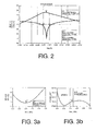
Figure 2 .- shows a diagram of the insertion losses (from ports 1-2, S(2,1) and ports 1-3, S(3,1) and return losses S(1,1). The scattering parameters S(2,1) and S(3,1) represent the transmision coefficient between the input port (1) and the output ports (2 and 3) respectively. This parameters are related with the gain of the structure. As can be seen the maximum gain is obtained in the vicinity of 2.45GHz, which is the interest operation frequency band. S(1,1) corresponds to the reflection atport 1. -
Figure 3 .- diagram (a) shows a simulated noise figure with a load impedance matched at the output ports , and diagram (b) shows the output differential phase vs frequency. -
Figure 1 shows a preferred embodiment of a LNA according to the present invention, which comprises a first circuit branch formed by a first transistor (M1) and a second transistor (M2) located in cascade configuration to amplify an input signal. - The first and the second transistors (M1,M2) are arranged as common source transistors, and a first LC tank is connected between the drain of the first transistor (M1) and the source of the second transistor (M2), to choke a signal between said nodes of the first and second transistors.
- The first LC tank is formed by a first inductor (Lt1), corresponding to a part of a transformer (T1) and a first tank capacitor (Ctl) connected in parallel, the value of said inductor, transformer coupling factor, and capacitor being calculated to provide a high impedance at the resonant frequency of the LC tank. The ideal coupling factor of the transformer is 1, although in practical embodiments it may be less than 1, for instance 0.7.
- The drain of the first transistor (M1) is coupled to the gate of the second transistor (M2) through a first capacitor (Cint) selected to apply or transfer a RF signal at the drain of the first transistor (M1) to the gate of the second transistor (M2).
- An input terminal (RFin) to receive said input signal, is coupled to the gate of the first transistor (M1) through a matching network formed by a first and a second matching capacitors (C1,C2) and a matching inductor (Lg) connected in a π-configuration. Alternatively the matching network can be connected in a T-configuration. This matching network is used to deliver maximum amount of power transference from the input terminal (RFin) to the LNA and to minimise noise power.
- A series decoupling capacitor (Cin) is connected between the matching network and the gate of the first transistor (M1), in order to avoid DC contribution over the RF input.
- In this preferred embodiment, the low noise amplifier comprises a first and second symmetric circuit branches to form a differential amplifier having a single input terminal (Rfin) and differential output terminals (Rfout+,Rfout-). Then, a second circuit branch comprises third and fourth transistors (M3,M4) coupled also in a cascaded configuration, are arranged as common source transistors. The drain of the third transistor (M3) is coupled to the gate of the fourth transistor (M4) through a second capacitor (Cint), to transfer a RF signal to the gate of the fourth transistor (M4). As it can be observed in
figure 1 , after the first amplifying stage, the implementation of the amplifier is fully symmetrical to ensure a good differential performance of the amplifier. - A second LC tank, connected between the drain of the third transistor (M3) and the source of the fourth transistor (M4), is formed by a second inductor (Lt1'), corresponding to a part of the transformer (T1) and a second tank capacitor (Ct1') connected in parallel, that is also calculated to provide a high impedance at the resonant frequency of the LC tank and avoid signal transmission between said nodes of the transistors.
- The first and the second LC tanks are the windings of a differential transformer (T1), and two capacitors (Ct1,Ct1') are connected in parallel and are tuned at the desired frequency (in this case 2.45 GHz), to avoids RF signal transmission between (M2-M4) sources and (M1-M3) drains.
- The gate of the third transistor (M3) is coupled to the drain of the first transistor (M1) by means of a third capacitor (Cdiff), which value is selected to copy the RF signal from one branch to the other one, and at the same time block the DC current.
- First and second shunt capacitors (Cs,Cs') are respectively connected in shunt configuration with capacitance Cgs (capacitance gate-source) of transistors (M1) and (M3) in order to increase matching controllability and improve noise figure. In particular, shunt capacitors (Cs,Cs') are respectively connected between the gate and the source of the first and third transistors (M1,M3). Capacitors (Cs,Cs') are included in the input matching and allow a certain degree of controllability since they increase the effective Cgs of transistors (M1,M3).
- The drains of the second and fourth transistors (M2,M4) are coupled respectively to output terminals (RFout+, RFin-), preferably by means of first and second output capacitors (Cout,Cout'), in order to avoid DC contribution over the differential output. The output terminals (RFout+, RFin-) provide a 180° differential output.
- In this embodiment, the drains of the second and fourth transistors (M2,M4) are connected to a DC supply source through a second differential transformer (T2) formed by third and fourth coupled inductors (Lt2,Lt2'). This second transformer (T2) is used to provide output matching and to perform good 180° output differential signal.
- The ideal coupling factor of (T1) and (T2) is 1, but in practial implementations the coupling factor of the transformers is lower than 1. The simulations have been performed with a coupling factor of 0.7.
- More in detail, the third inductor (Lt2) is connected between the drain of the second transistor (M2) and the DC power supply, and the fourth inductor (Lt2') is connected between the drain of the fourth transistor (M4) and the power supply. Third and fourth inductors (Lt2,Lt2') are connected in parallel respectively with third and fourth tank capacitors (Ct2,Ct2'), to form LC tanks respectively in the first and second circuit branches to avoid RF signal transmission to the DC power supply.
- A bypass capacitor (Cbypass) is connected between ground and the sources of the second and fourth transistors (M2,M4), to provide a reliable path to ground for the RF signal.
- The sources of the first and third transistors (M1,M3) are coupled to ground, through a degeneration inductor (Ls). The degeneration inductor (Ls) provides also another degree of freedom with regard to impedance matching. Moreover, it is designed to increase the impedance at node formed by (M1,M3) sources, because it improves the balanced gain and phase of the device. The reason to increase this node impedance is due to the fact that although the symmetric circuit configuration provides ideal 180° phase difference between branches, gain and phase could be degraded if this impedance is not controlled.
- In this amplifier, the first and the third inductors (Lt1,Lt2) and the degeneration inductor (Ls), provide a dc current path from the dc power supply to ground. Similarly in the second circuit branch, the second and fourth inductors (Lt1',Lt2') and (Ls) also provide a dc current path from the dc power supply to ground. Therefore, in this arrangement the same DC current is used for the pair of transistors (M1-M2) and for the pair of transistors (M3-M4), therefore saving power compared with cascaded amplifiers topologies. The current for each branch is equivalent if they are designed symmetrically.
- The second amplification stage formed by transistors (M2,M4) stacked over the first amplification stage (M1,M3), reduce the noise impact in the structure and increase the LNA gain. The circuit of this implementation is fully symmetrical from the first amplification stage to the voltage supply.
- Transistor biasing is carried out in a conventional voltage bias manner. In particular, first and second biasing resistors (Rbias1,Rbias1') are connected respectively between the gate nodes of the first and third transistors (M1,M3) and a first biasing voltage terminal (Vbias1). Third and fourth biasing resistors (Rbias2,Rbias2'), are connected respectively between the gate nodes of the second and fourth transistors (M2,M4) and a second biasing voltage terminal (Vbias2)..
- It is significant to note that the (M2-M4) stage may present the role of any cascade gain stage following a first amplifier formed by (M1-M3), since the bypass capacitor (Cbypass) provides a path to ground for the RF signal. In particular, the (M2-M4) stage could play the role of the transconductance stage of a following mixer device. In other words, this structure can be seen just as a LNA or a LNA with part of a mixer stage requiring the same power consumption.
- From S-parameters simulations according to
figure 2 , it can be observed a good matching (S(1,1)<15dB) and high gain performance (S(2,1)=16dB) as well as good noise figure performance (NF<4dB) and excellent differential output with 180.0°±0.1° accuracy in the operation frequency range. - The invention also refers to an integrated circuit and to a wireless communication device, including a low noise amplifier according to the present invention.
- The invention allows the use of a good quality transformer instead of a conventional inductor, thereby also reducing the surface required in a semiconductor die.
- Further embodiments of the invention are described in the attached dependent claims.
- The invention has been described according to some preferred embodiments of it, but for a skilled person in the art, it will be clear that many variations may be made to the preferred embodiments without departing from the object of the claimed invention.
Claims (26)
- A low noise amplifier including at least a first circuit branch, said first circuit branch comprising a first transistor (M1) and a second transistor (M2) connected in cascaded configuration to amplify an input signal, characterised in that it further comprises a first LC tank connected between the drain of the first transistor (M1) and the source of the second transistor (M2), wherein the LC tank is calculated to choke signal transmission.
- Low noise amplifier according to claim 1 wherein the first and the second transistors (M1,M2) are arranged as common source transistors.
- Low noise amplifier according to claim 1 or claim 2 wherein the drain of the first transistor (M1) is coupled to the gate of the second transistor (M2) through a first capacitor (Cint) selected to apply a signal at the drain of the first transistor to the gate of the second transistor.
- Low noise amplifier according to any of the preceding claims wherein it comprises an input terminal (RFin) to receive said input signal, and wherein said input terminal is coupled to the gate of the first transistor (M1).
- Low noise amplifier according to claim 4 wherein said input terminal is connected to the gate of the first transistor through a matching network, said matching network comprising a first and second matching capacitors (C1,C2) and a matching inductor (Lg) connected in a π-configuration or in a T-configuration.
- Low noise amplifier according to claim 4 or 5 wherein the matching network is connected between said input terminal (Rfin) and the gate of the first transistor.
- Low noise amplifier according to claim 6 wherein a series capacitor (Cin) is connected between the matching network and the gate of the first transistor, to avoid DC contribution over the RF input.
- Low noise amplifier according to any of the preceding claims wherein it comprises a first and second symmetric circuit branches to form a differential amplifier, having a single input terminal (Rfin) and differential output terminals (Rfout+,Rfout-).
- Low noise amplifier according to claim 8 wherein the second circuit branch comprises third and fourth transistors (M3,M4) connected in a cascaded configuration and arranged as common source transistors, wherein the drain of the third transistor (M3) is coupled to the gate of the fourth transistor (M4) through a second capacitor (Cint'), and wherein a second LC tank is connected between the drain of the third transistor (M3) and the source of the fourth transistor (M4).
- Low noise amplifier according to claim 9 wherein the gate of the third transistor (M3) is coupled to the drain of the first transistor (M1) by means of a third capacitor (Cdiff).
- Low noise amplifier according to claims 9 or 10 wherein a first and a second shunt capacitors (Cs,Cs') are respectively connected between the gate and the source of the first and third transistors (M1,M3).
- Low noise amplifier according to any of the preceding claims wherein the first LC tank is formed by a first inductor (Lt1) and a first tank capacitor (Ct1) connected in parallel, the LC tank being calculated to provide high impedance at the resonant frequency of the LC tank to avoid signal transmission.
- Low noise amplifier according to any of the claims 9 to 12 wherein the second LC tank is formed by a second inductor (Lt1') and a second tank capacitor (Ct1') connected in parallel, the LC tank being calculated to provide a high impedance at the resonant frequency of the LC tank to avoid signal transmission.
- Low noise amplifier according to claims 12 and 13 wherein the first and the second inductors (Lt1,Lt1') are coupled and are the windings of a first transformer (T1).
- Low noise amplifier according to any of the claims 9 to 14 wherein the drains of the second and fourth transistors (M2,M4) are coupled respectively to output terminals (RFout+,RFout-) to provide a differential output.
- Low noise amplifier according to claim 15 wherein the drains of the second and fourth transistors are coupled to the output terminals (RFout+,RFout-) respectively by means of first and second output capacitors (Cout,Cout').
- Low noise amplifier according to any of the claims 9 to 16, wherein the sources of the first and third transistors (M1,M3) are coupled to ground.
- Low noise amplifier according to claim 17 wherein the sources of the first and third transistors are connected to ground through a degeneration inductor (Ls).
- Low noise amplifier according to any of the claims 9 to 18, wherein the drains of the second and fourth transistors (M2,M4) are supplied by a DC source.
- Low noise amplifier according to claim 19 wherein the drains of the second and fourth transistors are connected to a DC supply through a second differential transformer (T2) formed by third and fourth inductors (Lt2,Lt2').
- Low noise amplifier according to claim 20 wherein the third inductor (Lt2) is connected between the drain of the second transistor (M2) and the DC power supply, and the fourth inductor (Lt2') is connected between the drain of the fourth transistor (M4) and the power supply.
- Low noise amplifier according to claim 20 or 21, wherein the third and fourth inductors (Lt2,Lt2') are connected in parallel respectively with third and fourth tank capacitors (Ct2,Ct2'), to form a LC tanks in the first and second circuit branches to provide a RF choke.
- Low noise amplifier according to any of the claims 9 to 22 wherein a bypass capacitor (Cbypass) is connected between ground and the sources of the second and fourth transistors (M2,M4), to provide a path to ground for the RF signal.
- Low noise amplifier according to any of the preceding claims wherein it is adapted to operate within a band having a central frequency of approximately 2.45 GHz.
- Integrated circuit having a semiconductor die including at least one low noise amplifier according to any of the claims 1 to 24.
- wireless communication device including a low noise amplifier according to any of the claims 1 to 24.
Priority Applications (1)
| Application Number | Priority Date | Filing Date | Title |
|---|---|---|---|
| EP07116605A EP2037573A1 (en) | 2007-09-17 | 2007-09-17 | Ultra-low power consumption low noise amplifier |
Applications Claiming Priority (1)
| Application Number | Priority Date | Filing Date | Title |
|---|---|---|---|
| EP07116605A EP2037573A1 (en) | 2007-09-17 | 2007-09-17 | Ultra-low power consumption low noise amplifier |
Publications (1)
| Publication Number | Publication Date |
|---|---|
| EP2037573A1 true EP2037573A1 (en) | 2009-03-18 |
Family
ID=38962005
Family Applications (1)
| Application Number | Title | Priority Date | Filing Date |
|---|---|---|---|
| EP07116605A Withdrawn EP2037573A1 (en) | 2007-09-17 | 2007-09-17 | Ultra-low power consumption low noise amplifier |
Country Status (1)
| Country | Link |
|---|---|
| EP (1) | EP2037573A1 (en) |
Cited By (13)
| Publication number | Priority date | Publication date | Assignee | Title |
|---|---|---|---|---|
| CN101807883A (en) * | 2010-04-08 | 2010-08-18 | 复旦大学 | Single-ended input and differential output low-noise amplifier applied in UWB system |
| CN102801389A (en) * | 2012-08-30 | 2012-11-28 | 东南大学 | Ultra-low power consumption low-noise amplifier |
| WO2014008189A3 (en) * | 2012-07-06 | 2014-02-27 | Analog Devices, Inc. | Common mode bias circuit |
| TWI454052B (en) * | 2011-04-01 | 2014-09-21 | Realtek Semiconductor Corp | Single-ended to double-ended circuit |
| EP2913922A1 (en) * | 2014-02-28 | 2015-09-02 | Telefonaktiebolaget L M Ericsson (publ) | A low noise amplifier circuit |
| KR101694075B1 (en) * | 2015-11-11 | 2017-01-06 | 이화여자대학교 산학협력단 | Differential Trans-impedance Amplifier |
| CN108880481A (en) * | 2017-05-16 | 2018-11-23 | 博通集成电路(上海)股份有限公司 | Low noise amplifier, receiver and method for low noise amplifier |
| EP3462609A1 (en) * | 2017-09-29 | 2019-04-03 | NXP USA, Inc. | Radio frequency (rf) receiver circuit |
| CN111446928A (en) * | 2019-01-16 | 2020-07-24 | 三星电机株式会社 | Inductor and low noise amplifier including the same |
| CN112514248A (en) * | 2018-05-30 | 2021-03-16 | 斯威特科技有限公司 | Wideband Low Noise Amplifier (LNA) with reconfigurable bandwidth for millimeter wave 5G communications |
| WO2023082932A1 (en) * | 2021-10-18 | 2023-05-19 | 深圳飞骧科技股份有限公司 | Low-noise amplifier, related device and chip |
| CN116192067A (en) * | 2023-04-28 | 2023-05-30 | 广东工业大学 | A Power Amplifier with Enhanced Voltage Swing in Transistor Stacks |
| CN119401953A (en) * | 2024-10-16 | 2025-02-07 | 中山大学 | A low noise amplifier structure using multi-inductor coupling and current multiplexing |
Citations (5)
| Publication number | Priority date | Publication date | Assignee | Title |
|---|---|---|---|---|
| DE4031642A1 (en) * | 1989-10-06 | 1991-04-18 | Alps Electric Co Ltd | TWO-STAGE DIFFERENTIAL AMPLIFIER IN CASCADE |
| US6122532A (en) * | 1998-11-18 | 2000-09-19 | Triquint Semiconductor Corporation | RF amplifier with reduced power consumption |
| US6133793A (en) * | 1998-07-27 | 2000-10-17 | Motorola, Inc. | Circuit and method of amplifying a signal for a receiver |
| US6366171B1 (en) * | 2000-04-06 | 2002-04-02 | Texas Instruments Incorporated | Single-to-differential low noise amplifier |
| US20030141953A1 (en) * | 2002-01-28 | 2003-07-31 | Haslett James William | Monolithic transformer compensated circuit |
-
2007
- 2007-09-17 EP EP07116605A patent/EP2037573A1/en not_active Withdrawn
Patent Citations (5)
| Publication number | Priority date | Publication date | Assignee | Title |
|---|---|---|---|---|
| DE4031642A1 (en) * | 1989-10-06 | 1991-04-18 | Alps Electric Co Ltd | TWO-STAGE DIFFERENTIAL AMPLIFIER IN CASCADE |
| US6133793A (en) * | 1998-07-27 | 2000-10-17 | Motorola, Inc. | Circuit and method of amplifying a signal for a receiver |
| US6122532A (en) * | 1998-11-18 | 2000-09-19 | Triquint Semiconductor Corporation | RF amplifier with reduced power consumption |
| US6366171B1 (en) * | 2000-04-06 | 2002-04-02 | Texas Instruments Incorporated | Single-to-differential low noise amplifier |
| US20030141953A1 (en) * | 2002-01-28 | 2003-07-31 | Haslett James William | Monolithic transformer compensated circuit |
Non-Patent Citations (3)
| Title |
|---|
| DARIUSZ PIENKOWSKI ET AL: "A 3.6 dB NF, 6 GHz band CMOS LNA with 3.6 mW power consumption", WIRELESS TECHNOLOGY, 2006. THE 9TH EUROPEAN CONFERENCE ON, IEEE, PI, September 2006 (2006-09-01), pages 67 - 70, XP031005241, ISBN: 2-9600551-5-2 * |
| DEVLIN L M ET AL: "A 2.4 GHz single chip transceiver", MICROWAVE AND MILLIMETER-WAVE MONOLITHIC CIRCUITS SYMPOSIUM, 1993. DIGEST OF PAPERS., IEEE 1993 ATLANTA, GA, USA 14-15 JUNE 1993, NEW YORK, NY, USA,IEEE, US, 14 June 1993 (1993-06-14), pages 23 - 26, XP010069076, ISBN: 0-7803-1322-4 * |
| LIAO C-H ET AL: "A 5.7-GHZ 0.18-MUM CMOS GAIN-CONTROLLED DIFFERENTIAL LNA WITH CURRENT REUSE FOR WLAN RECEIVER", IEEE MICROWAVE AND WIRELESS COMPONENTS LETTERS, IEEE SERVICE CENTER, NEW YORK, NY, US, vol. 13, no. 12, December 2003 (2003-12-01), pages 526 - 528, XP001190047, ISSN: 1531-1309 * |
Cited By (24)
| Publication number | Priority date | Publication date | Assignee | Title |
|---|---|---|---|---|
| CN101807883A (en) * | 2010-04-08 | 2010-08-18 | 复旦大学 | Single-ended input and differential output low-noise amplifier applied in UWB system |
| TWI454052B (en) * | 2011-04-01 | 2014-09-21 | Realtek Semiconductor Corp | Single-ended to double-ended circuit |
| WO2014008189A3 (en) * | 2012-07-06 | 2014-02-27 | Analog Devices, Inc. | Common mode bias circuit |
| US8803602B2 (en) | 2012-07-06 | 2014-08-12 | Analog Devices, Inc. | Common mode bias circuit |
| CN102801389A (en) * | 2012-08-30 | 2012-11-28 | 东南大学 | Ultra-low power consumption low-noise amplifier |
| US10454431B2 (en) | 2014-02-28 | 2019-10-22 | Telefonaktiebolaget L M Ericsson (Publ) | Low noise amplifier circuit |
| EP2913922A1 (en) * | 2014-02-28 | 2015-09-02 | Telefonaktiebolaget L M Ericsson (publ) | A low noise amplifier circuit |
| US12375044B2 (en) | 2014-02-28 | 2025-07-29 | Telefonaktiebolaget Lm Ericsson (Publ) | Low noise amplifier circuit |
| US11057005B2 (en) | 2014-02-28 | 2021-07-06 | Telefonaktiebolaget Lm Ericsson (Publ) | Low noise amplifier circuit |
| KR101694075B1 (en) * | 2015-11-11 | 2017-01-06 | 이화여자대학교 산학협력단 | Differential Trans-impedance Amplifier |
| WO2017082575A1 (en) * | 2015-11-11 | 2017-05-18 | 이화여자대학교 산학협력단 | Differential transmission impedance amplifier |
| CN108880481A (en) * | 2017-05-16 | 2018-11-23 | 博通集成电路(上海)股份有限公司 | Low noise amplifier, receiver and method for low noise amplifier |
| CN108880481B (en) * | 2017-05-16 | 2021-10-08 | 博通集成电路(上海)股份有限公司 | Low noise amplifier, receiver for low noise amplifier and method |
| US10447206B2 (en) | 2017-09-29 | 2019-10-15 | Nxp Usa, Inc. | Radio frequency (RF) receiver circuit |
| EP3462609A1 (en) * | 2017-09-29 | 2019-04-03 | NXP USA, Inc. | Radio frequency (rf) receiver circuit |
| CN109586742A (en) * | 2017-09-29 | 2019-04-05 | 恩智浦美国有限公司 | Rf reception device circuit |
| CN109586742B (en) * | 2017-09-29 | 2022-08-05 | 恩智浦美国有限公司 | Radio Frequency (RF) receiver circuit |
| CN112514248A (en) * | 2018-05-30 | 2021-03-16 | 斯威特科技有限公司 | Wideband Low Noise Amplifier (LNA) with reconfigurable bandwidth for millimeter wave 5G communications |
| CN111446928A (en) * | 2019-01-16 | 2020-07-24 | 三星电机株式会社 | Inductor and low noise amplifier including the same |
| CN111446928B (en) * | 2019-01-16 | 2024-03-26 | 三星电机株式会社 | Inductor and low noise amplifier including the inductor |
| WO2023082932A1 (en) * | 2021-10-18 | 2023-05-19 | 深圳飞骧科技股份有限公司 | Low-noise amplifier, related device and chip |
| CN116192067A (en) * | 2023-04-28 | 2023-05-30 | 广东工业大学 | A Power Amplifier with Enhanced Voltage Swing in Transistor Stacks |
| CN116192067B (en) * | 2023-04-28 | 2023-08-15 | 广东工业大学 | A Power Amplifier with Enhanced Voltage Swing in Transistor Stacks |
| CN119401953A (en) * | 2024-10-16 | 2025-02-07 | 中山大学 | A low noise amplifier structure using multi-inductor coupling and current multiplexing |
Similar Documents
| Publication | Publication Date | Title |
|---|---|---|
| EP2037573A1 (en) | Ultra-low power consumption low noise amplifier | |
| CN102355200B (en) | Single-ended input and differential output parallel dual-frequency low noise amplifier and design method thereof | |
| KR102557851B1 (en) | Transmit and Receive Switches and Broadband Power Amplifier Matching Networks for Multi-Band Millimeter Wave 5G Communications | |
| US9935585B2 (en) | RF amplifier operational in different power modes | |
| CN104779919A (en) | Self-biased ultra wideband low-power-consumption low-noise amplifier (LNA) | |
| US8437723B2 (en) | Amplifier circuit and communication device | |
| CN114094955A (en) | W-waveband high-gain low-noise amplifier circuit | |
| CN107408927A (en) | Amplifiers for Noise Suppression | |
| Reja et al. | An area-efficient multistage 3.0-to 8.5-GHz CMOS UWB LNA using tunable active inductors | |
| CN118399899A (en) | Millimeter wave frequency band double-circuit synthesized bidirectional amplifier, chip and electronic equipment | |
| CN105071778B (en) | A kind of Terahertz power amplifier realized based on CMOS technology | |
| Li et al. | A 4.5–8.5 GHz GaAs power amplifier with high in-band flatness | |
| US20260058617A1 (en) | Low noise amplifier incorporating sutardja transformer | |
| US20080231383A1 (en) | Origami Cascaded Topology For Analog and Mixed-Signal Applications | |
| EP2037572A1 (en) | Ultra-low power consumption current-reused front-end for a RF system | |
| Cheng et al. | A 1.4-mW Ka-band Low Noise Amplifier Using Self-Resonant Transformer Matching in 90-nm CMOS Process | |
| Li et al. | A novel design approach for GHz CMOS low noise amplifiers | |
| Spandana et al. | Design and performance analysis of low noise amplifiers: A review | |
| CN112436810A (en) | Low noise amplifier, receiver and electronic equipment based on inverter | |
| Heller et al. | Analysis of cross-coupled common-source cores for W-band LNA design at 28nm CMOS | |
| Wan et al. | A V-band Power Amplifier for Satellite Communications in 40-nm CMOS | |
| Ninan et al. | Design and analysis of low noise amplifier at 60 GHz using active feedback and current re-use topologies | |
| US20260074658A1 (en) | Noise-cancellation amplifier | |
| Lee et al. | 90 GHz Power Amplifier in 150nm GaAs Process | |
| Saraswat et al. | Doherty Power Amplifier Based TR front end Network for 5G Mm-Wave Applications |
Legal Events
| Date | Code | Title | Description |
|---|---|---|---|
| PUAI | Public reference made under article 153(3) epc to a published international application that has entered the european phase |
Free format text: ORIGINAL CODE: 0009012 |
|
| AK | Designated contracting states |
Kind code of ref document: A1 Designated state(s): AT BE BG CH CY CZ DE DK EE ES FI FR GB GR HU IE IS IT LI LT LU LV MC MT NL PL PT RO SE SI SK TR |
|
| AX | Request for extension of the european patent |
Extension state: AL BA HR MK RS |
|
| AKX | Designation fees paid | ||
| REG | Reference to a national code |
Ref country code: DE Ref legal event code: 8566 |
|
| STAA | Information on the status of an ep patent application or granted ep patent |
Free format text: STATUS: THE APPLICATION IS DEEMED TO BE WITHDRAWN |
|
| 18D | Application deemed to be withdrawn |
Effective date: 20090919 |