EP2026355A2 - System and method for implementing a memory defect map - Google Patents
System and method for implementing a memory defect map Download PDFInfo
- Publication number
- EP2026355A2 EP2026355A2 EP08014498A EP08014498A EP2026355A2 EP 2026355 A2 EP2026355 A2 EP 2026355A2 EP 08014498 A EP08014498 A EP 08014498A EP 08014498 A EP08014498 A EP 08014498A EP 2026355 A2 EP2026355 A2 EP 2026355A2
- Authority
- EP
- European Patent Office
- Prior art keywords
- memory
- defect map
- defective
- map
- defect
- Prior art date
- Legal status (The legal status is an assumption and is not a legal conclusion. Google has not performed a legal analysis and makes no representation as to the accuracy of the status listed.)
- Granted
Links
- 230000007547 defect Effects 0.000 title claims abstract description 114
- 238000000034 method Methods 0.000 title claims abstract description 35
- 230000002950 deficient Effects 0.000 claims abstract description 91
- 238000013467 fragmentation Methods 0.000 claims description 6
- 238000006062 fragmentation reaction Methods 0.000 claims description 6
- 230000009977 dual effect Effects 0.000 claims description 2
- 238000010586 diagram Methods 0.000 description 8
- 238000013507 mapping Methods 0.000 description 6
- 230000008901 benefit Effects 0.000 description 5
- 238000012545 processing Methods 0.000 description 5
- 230000008569 process Effects 0.000 description 4
- 238000004891 communication Methods 0.000 description 3
- 238000005516 engineering process Methods 0.000 description 3
- 238000013500 data storage Methods 0.000 description 2
- 230000005055 memory storage Effects 0.000 description 2
- 230000002411 adverse Effects 0.000 description 1
- 230000004075 alteration Effects 0.000 description 1
- 230000001668 ameliorated effect Effects 0.000 description 1
- 230000006399 behavior Effects 0.000 description 1
- 230000000694 effects Effects 0.000 description 1
- 230000006870 function Effects 0.000 description 1
- 230000014759 maintenance of location Effects 0.000 description 1
- 238000007726 management method Methods 0.000 description 1
- 230000007246 mechanism Effects 0.000 description 1
- 239000000203 mixture Substances 0.000 description 1
- 230000006855 networking Effects 0.000 description 1
- 230000009467 reduction Effects 0.000 description 1
- 238000012552 review Methods 0.000 description 1
- 239000007787 solid Substances 0.000 description 1
- 238000006467 substitution reaction Methods 0.000 description 1
- 238000012360 testing method Methods 0.000 description 1
Images


Classifications
-
- G—PHYSICS
- G11—INFORMATION STORAGE
- G11C—STATIC STORES
- G11C5/00—Details of stores covered by group G11C11/00
- G11C5/02—Disposition of storage elements, e.g. in the form of a matrix array
- G11C5/04—Supports for storage elements, e.g. memory modules; Mounting or fixing of storage elements on such supports
-
- G—PHYSICS
- G11—INFORMATION STORAGE
- G11C—STATIC STORES
- G11C29/00—Checking stores for correct operation ; Subsequent repair; Testing stores during standby or offline operation
- G11C29/70—Masking faults in memories by using spares or by reconfiguring
- G11C29/78—Masking faults in memories by using spares or by reconfiguring using programmable devices
- G11C29/80—Masking faults in memories by using spares or by reconfiguring using programmable devices with improved layout
- G11C29/808—Masking faults in memories by using spares or by reconfiguring using programmable devices with improved layout using a flexible replacement scheme
-
- G—PHYSICS
- G11—INFORMATION STORAGE
- G11C—STATIC STORES
- G11C29/00—Checking stores for correct operation ; Subsequent repair; Testing stores during standby or offline operation
- G11C29/04—Detection or location of defective memory elements, e.g. cell constructio details, timing of test signals
- G11C2029/0407—Detection or location of defective memory elements, e.g. cell constructio details, timing of test signals on power on
-
- G—PHYSICS
- G11—INFORMATION STORAGE
- G11C—STATIC STORES
- G11C29/00—Checking stores for correct operation ; Subsequent repair; Testing stores during standby or offline operation
- G11C29/04—Detection or location of defective memory elements, e.g. cell constructio details, timing of test signals
- G11C2029/0409—Online test
-
- G—PHYSICS
- G11—INFORMATION STORAGE
- G11C—STATIC STORES
- G11C29/00—Checking stores for correct operation ; Subsequent repair; Testing stores during standby or offline operation
- G11C29/56—External testing equipment for static stores, e.g. automatic test equipment [ATE]; Interfaces therefor
- G11C2029/5606—Error catch memory
Definitions
- the present disclosure relates generally to computing systems and information handling systems, and, more particularly, to a system and method for creating a map of memory which governs its use by the computing system or information handling system.
- An information handling system generally processes, compiles, stores, and/or communicates information or data for business, personal, or other purposes thereby allowing users to take advantage of the value of the information. Because technology and information handling needs and requirements vary between different users or applications, information handling systems may vary with respect to the type of information handled; the methods for handling the information; the methods for processing, storing or communicating the information; the amount of information processed, stored, or communicated; and the speed and efficiency with which the information is processed, stored, or communicated.
- information handling systems allow for information handling systems to be general or configured for a specific user or specific use such as financial transaction processing, airline reservations, enterprise data storage, or global communications.
- information handling systems may include or comprise a variety of hardware and software components that may be configured to process, store, and communicate information and may include one or more computer systems, data storage systems, and networking systems.
- An information handling system will typically include some type of temporary information storage medium, such as random access memory.
- the amount of memory included in an information handling system may be on the order of gigabytes. As memory size increases, the likelihood that part of the memory will either be manufactured defective or become defective over time increases. If left unmanaged, the presence of defective memory cells, regardless of their size, can cause the information handling system to fail. Such failure can initiate an abrupt end to the current operation of the information handling system, resulting in the loss of critical data. A memory failure could also prevent the information handling system from starting up altogether.
- a system and method are herein disclosed for managing memory defects in an information handling system.
- a first quantity of memory such as RAM
- a second quantity of memory such as EEPROM
- the memory defect map may then be referenced by the BIOS or the operating system to preclude use of regions of memory containing defective memory elements.
- the system and method disclosed herein are technically advantageous because a mechanism is provided for reducing the functional and financial impact of defective memory elements.
- the present disclosure provides a way for an information handling system to operate normally, despite the presence of one or more defective memory elements, with minimal impact on system performance. By effectively hiding defective memory blocks from the operating system, crashes of the information handling system are better avoided.
- the present disclosure extends the life of memory. Overall system costs for the information handling system are correspondingly reduced as memory need not be replaced even after multiple memory elements are found to be defective. Other technical advantages will be apparent to those of ordinary skill in the art in view of the following specification, claims, and drawings.
- an information handling system may include any instrumentality or aggregate of instrumentalities operable to compute, classify, process, transmit, receive, retrieve, originate, switch, store, display, manifest, detect, record, reproduce, handle, or utilize any form of information, intelligence, or data for business, scientific, control, or other purposes.
- an information handling system may be a personal computer, a network storage device, or any other suitable device and may vary in size, shape, performance, functionality, and price.
- the information handling system may include random access memory (RAM), one or more processing resources such as a central processing unit (CPU) or hardware or software control logic, ROM, and/or other types of nonvolatile memory.
- Additional components of the information handling system may include one or more disk drives, one or more network ports for communication with external devices as well as various input and output (I/O) devices, such as a keyboard, a mouse, and a video display.
- the information handling system may also include one or more buses operable to transmit communications between the various hardware components.
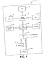
- FIG. 1 Shown in Figure 1 is a block diagram of a typical information handling system.
- a processor or CPU 12 of the typical information handling system 10 is communicatively coupled to a memory controller hub or north bridge 30.
- Memory controller hub 30 is coupled to RAM 20 and a graphics processing unit 40.
- Memory controller hub 30 is also coupled to an I/O controller hub or south bridge 60.
- I/O hub 60 is coupled to storage elements of the computer system, including a storage element 50, which may comprise a flash ROM that includes the BIOS of the computer system.
- I/O hub 60 is also coupled to the hard drive 70 of the computer system.
- I/O hub 60 may also be coupled to a Super I/O chip 80, which is itself coupled to several of the I/O ports of the computer system, including keyboard 90, mouse 100, and one or more parallel ports.
- the system and method described herein involve the management of the memory resources of an information handling system.
- the system and method involve the use of storage included within memory devices to identify which, if any, of the physical memory of the memory device is unusable by the system. If physical memory is identified as being unusable by the system, the physical memory is logically mapped out of a resulting memory map of the usable computer system, resulting in a memory map of usable memory that does not include the defective physical memory of the memory device.
- FIG. 2A is a diagram of the memory space that is reviewed by a memory mapping call, such as an E820 call, within the information handling system.
- the information handling system 10 may be comprised of numerous distinct components capable of being addressed as memory, including dual-inline memory modules (DIMMs) 120 and PCI devices 130, such as discrete graphics cards. Devices that include addressable memory are detected during the BIOS initialization period, and the memory within these devices is mapped and identified as system-accessible memory during the memory mapping call.
- a memory mapping call results in the iterative interrogation of possible memory locations, beginning with memory having the lowest possible address within the system 110.
- the memory mapping call reviews all addressable memory locations, including memory blocks 124, 125 and 126, even though memory block 125 contains a memory defect As system-accessible memory is located, including DIMMs 120, a map is created of usable, non-defective memory.
- FIG. 2B is a diagram of a usable memory map in which the unusable locations in the memory of the computer system have been logically mapped out of the computer system. For example, memory blocks 124 and 126 are included in the usable memory map, but memory block 125, which contains a defective memory element, is not.
- the usable memory map is acquired by the operating system, either as a result of a set of iterative memory mapping calls by the operating system or as a result of a memory mapping function in which the BIOS transmits the completed map to the operating system. Because the map excludes from its scope those physical memory locations that are determined to be unavailable or defective, the operating system is only able to access the memory that is mapped as being usable. Physical memory that is mapped as being unusable cannot be used by the operating system and can therefore be described as being not visible by the operating system.
- information regarding the location of usable memory regions is sent to the operating system. This information may take the form of a starting address, the size of the memory block in question, and the type of memory at that location. As defective memory blocks are carved or mapped out of the memory map, the memory map is divided into more pieces and the number of discrete entries that are required to describe the memory available (or unavailable) to the system increases, requiring additional storage and resulting in the fragmentation of memory. A number of strategies can be employed to reduce the administrative burden of identifying an excessive number of defective entries and usable entries.
- FIGS. 3A and 3B illustrate DIMMs 300 divided into memory blocks 310.
- a memory block is a defined section of contiguous storage within a memory device. Included within DIMMs 300 are defect blocks 320 and 340.
- a defect block is a memory block that includes at least some defective memory within the block.
- a defect block may include a mixture of defective memory and non-defective or usable memory. If defect blocks 320 and 340 were individually mapped out of the usable memory map, each block would be identified by a starting address and an ending address.
- Such fragmentation may be ameliorated by detecting the presence of small blocks of usable memory between defective memory blocks and grouping the small usable memory block together with the adjacent defective memory blocks and designating the entire group as unusable. This excludes additional non-defective memory from use by the information handling system, but it reduces the number of addresses that must be stored as part of the usable memory map.
- defect blocks 320 and 340 can be grouped into one larger defect block which includes non-defective memory block 330. Since only a single defect block is identified to the operating system, a single usable memory map entry is sufficient to map out both memory defects. To accomplish this reduction in fragmentation, the memory defect map is searched for defect blocks within some specified number of memory blocks from each other. When two such blocks are found, any intervening blocks are marked as defective. This information is subsequently stored in the memory defect map. When the information handling system is next initialized, the usable memory map will include only one entry for the contiguous memory blocks marked as defective, including the intervening non-defective memory block.
- FIG. 4 presents a block diagram of memory elements within DIMMs 400.
- a DIMM may include both RAM 410 and a quantity of electrically-erasable programmable read-only memory (EEPROM) 420, which comprises non-volatile storage that is included on DIMM 400.
- EEPROM 420 can store serial presence detect (SPD) information, which is data that describes the size, speed, electrical requirements, and other information about the RAM 410.
- SPD serial presence detect
- DIMMs typically include an additional instance of nonvolatile memory 440 that is not dedicated to SPD information and is referred to herein as memory defect storage 440.
- Memory defect storage 440 of EEPROM 420 is used to store information describing the location of defective memory in RAM 410.
- a memory cell is identified as defective or if it is otherwise determined that the system should not be granted access to that cell, a block of memory containing the memory cell in question is identified and the location of that memory is stored in memory defect storage 440.
- the placement of the defect memory storage in a DIMM has advantages in that the memory location within the DIMM is widely implemented in information handling systems and is available for the storage of this information. Moreover, the placement of the memory defect map within the DIMM itself is advantageous, as the memory defect information remains with the DIMM and allows the defect information for the DIMM to travel with the DIMM in the event that the DIMM moves from one computer system to another.
- memory defect storage 440 serves a dedicated location for the identification of defective memory locations, it is not necessary that the defect map be stored in a nonvolatile location within EEPROM 420. Rather, any form of non-volatile storage that is accessible by the computer system could be used to store the record of defective memory locations.
- the content of the memory defect storage location is a memory defect map, with each entry in the map corresponding to a region of the physical address on the associated DIMM 400.
- the size of each designated region in the map is defined by the memory capacity of the DIMM amortized across the number of entries permitted in the map.
- the size of memory block designated as defective is thus equal to the DIMM capacity divided by the number of bits in the defect map. The larger the available space for the memory defect map, the smaller the size of the memory block that can be designated as defective.
- each bit in the memory defect map in memory defect storage corresponds to one memory block in the DIMM.
- the size of the memory defect map can be adjusted as appropriate either to minimize the size of the memory map or to maximize the resolution of the memory map, which results in more usable memory. If storage space for the memory map is at a premium, the size of the map can be reduced by simply associating each bit in the memory map with a larger memory block in the RAM of the DIMM. If the maximization of usable memory is a more important consideration, the resolution and size of the memory map may be increased, resulting in finer granularity in identifying the defective memory cells, thereby resulting in fewer usable memory cells being grouped with the defective cell in each memory block and designated unusable as a result.
- the grouping of memory cells that are designated as being unusable, including defective memory cells and usable memory cells grouped with the defective memory cells, is known as the defect block.
- the defect block As an example, in a system that includes 4GB of RAM and the defect memory map is constrained to be 80 bytes (640 bits) in size, each time a defective memory cell is detected, 6.4MB (4GB/80 bytes) of memory is blocked out as unusable, even if only one cell is identified as being defective. Thus, increasing the size of the defect memory map may result in fewer usable memory cells being grouped with the defective memory cell and being designated as unusable.
- the defect map may be implemented with one byte per entry. This increases the size of the map considerably, but results in much less wasted memory for each defective cell.
- the defect map is initially indexed such that each entry in the defect map corresponds to one region of memory on the DIMM. Each entry in the defect map is eight bits in length. One bit of each eight-bit entry flags the region as one containing a defective bit. The remaining seven bits of each entry are used as an address for one or more sub-blocks within the designated memory region.
- each memory region corresponding to each eight-bit entry in the defect map is thus divided into 2 7 (128) sub-blocks, and seven bits of each entry are used as an address to point to the specific sub-block within the larger region that contains the defective memory cell.
- This type of map has the same trade-off between granularity and map size, but it provides an effective way to manage defect maps with much higher granularity.
- a defect map within a DIMM can be implemented when both high granularity and smaller map size are desired, if the number of defective regions is capped at a specific number.
- the size of each entry in the memory defect map is maximized based on the space available for the map and the number of defective regions chosen. For instance, if the SPD has sixty-four bytes (512 bits) available for the defect map and a limit of forty defective regions is chosen, each entry would be 512 bits divided by the forty available entries, resulting in 16 bits per entry. Unlike other examples, no bits are used to flag a region as defective or usable. Instead, all the bits are used as an offset pointer from the lowest memory address on the DIMM.
- Entries are populated serially as memory defects are found, and each populated entry indicates that the region beginning at the pointer contains a defective memory cell.
- This type of map has the advantages of increased granularity (resulting in less wasted memory per defect) and small map size, but the memory cannot support more than the chosen number of defective regions. Any additional defects would not be incorporated into the map, and could either be left unmanaged or could be managed by some other method.
- An information handling system may include multiple DIMMs.
- the memory defect map that is included in the memory storage locations of each of the DIMMs may be combined in the memory of the information handling system into a global memory defect map that identifies the defective memory of the entire information handling system.
- locations of defective memory are known and defective memory locations can be excluded during computing operations. If additional defective memory locations are discovered during operation of the information handling system, these locations are added to the global memory defect map on a real-time basis. If a defective memory location is discovered during operation of the information handling system, a defective memory pointer to the block of defective memory is established in system memory at memory address that is above or higher than the memory space of the DIMMs of the information handling system.
- the first one, two, or three bits of the entry are a DIMM index that identifies the DIMM that includes the defective memory block.
- the remaining bits of the defective memory pointer are a block index that identifies the location of the defective memory block within the affected DIMM.
- the block index is created by dividing the physical address of the defective memory cell on the DIMM by the defined block size of the defect block that has been established for the DIMMs of the information handling system. In this manner, an index is created, comprising an entry in memory that includes (a) an index to the DIMM that includes a defect and (b) an index to the memory block within the DIMM. After this pointer is created, the pointer is added to the global memory defect map, resulting in the defective memory block being excluded from operations in the information handling system.
- FIG. 5 is a flow diagram of the creation of a usable memory map.
- the power-on self-test (POST) phase begins at step 510.
- POST power-on self-test
- memory devices are identified and the defect maps for memory are retrieved from each respective device (step 520).
- a defect map is a memory map of defective memory locations at step 530.
- a usable memory map is created which excludes the memory locations that are identified in the memory defect map. Thus, even though a memory device includes defective memory, the locations of the defective memory are mapped out of the usable memory map that is created by the operating system.
- a magnetic storage device may be coupled to other non-volatile storage which contains a defect map for the magnetic storage device.
Abstract
Description
- The present disclosure relates generally to computing systems and information handling systems, and, more particularly, to a system and method for creating a map of memory which governs its use by the computing system or information handling system.
- As the value and use of information continues to increase, individuals and businesses seek additional ways to process and store information. One option available to these users is an information handling system. An information handling system generally processes, compiles, stores, and/or communicates information or data for business, personal, or other purposes thereby allowing users to take advantage of the value of the information. Because technology and information handling needs and requirements vary between different users or applications, information handling systems may vary with respect to the type of information handled; the methods for handling the information; the methods for processing, storing or communicating the information; the amount of information processed, stored, or communicated; and the speed and efficiency with which the information is processed, stored, or communicated. The variations in information handling systems allow for information handling systems to be general or configured for a specific user or specific use such as financial transaction processing, airline reservations, enterprise data storage, or global communications. In addition, information handling systems may include or comprise a variety of hardware and software components that may be configured to process, store, and communicate information and may include one or more computer systems, data storage systems, and networking systems.
- An information handling system will typically include some type of temporary information storage medium, such as random access memory. The amount of memory included in an information handling system may be on the order of gigabytes. As memory size increases, the likelihood that part of the memory will either be manufactured defective or become defective over time increases. If left unmanaged, the presence of defective memory cells, regardless of their size, can cause the information handling system to fail. Such failure can initiate an abrupt end to the current operation of the information handling system, resulting in the loss of critical data. A memory failure could also prevent the information handling system from starting up altogether.
- As information handling systems continue to evolve and computer technology advances, the operational relationship between the CPU and memory becomes more significant and complex. Many attributes of modem systems (specifically, the introduction of multi-core processors and virtualization) are contributing to an ever-larger memory footprint within a typical information handling system. Consequently, not only is system memory becoming a much more substantial percentage of the overall cost of the information handling solution, the impact of erroneous behavior in the memory can have a much more adverse effect on the life cycle expense associated with the information handling system.
- In accordance with the present disclosure, a system and method are herein disclosed for managing memory defects in an information handling system. In an information handling system, a first quantity of memory, such as RAM, may contain defective memory elements. A second quantity of memory, such as EEPROM, is physically coupled to the first quantity of memory and is used to store a memory defect map containing information regarding the location of defective memory elements in the first quantity of memory. The memory defect map may then be referenced by the BIOS or the operating system to preclude use of regions of memory containing defective memory elements.
- The system and method disclosed herein are technically advantageous because a mechanism is provided for reducing the functional and financial impact of defective memory elements. In particular, the present disclosure provides a way for an information handling system to operate normally, despite the presence of one or more defective memory elements, with minimal impact on system performance. By effectively hiding defective memory blocks from the operating system, crashes of the information handling system are better avoided. In addition, by sequestering defective memory elements, the present disclosure extends the life of memory. Overall system costs for the information handling system are correspondingly reduced as memory need not be replaced even after multiple memory elements are found to be defective. Other technical advantages will be apparent to those of ordinary skill in the art in view of the following specification, claims, and drawings.
- A more complete understanding of the present embodiments and advantages thereof may be acquired by referring to the following description taken in conjunction with the accompanying drawings, in which like reference numbers indicate like features, and wherein:
-
Figure 1 is a block diagram of a typical information handling system; -
Figure 2A shows the addressable memory space for a typical information handling system; -
Figure 2B shows the memory space included in a usable memory map which excludes defect blocks; -
Figures 3A and 3B depict the results of reducing fragmentation in a usable memory map; -
Figure 4 is a block diagram of two dual-inline memory modules; and -
Figure 5 shows a flow diagram from system initialization to the creation of a usable memory map. - For purposes of this disclosure, an information handling system may include any instrumentality or aggregate of instrumentalities operable to compute, classify, process, transmit, receive, retrieve, originate, switch, store, display, manifest, detect, record, reproduce, handle, or utilize any form of information, intelligence, or data for business, scientific, control, or other purposes. For example, an information handling system may be a personal computer, a network storage device, or any other suitable device and may vary in size, shape, performance, functionality, and price. The information handling system may include random access memory (RAM), one or more processing resources such as a central processing unit (CPU) or hardware or software control logic, ROM, and/or other types of nonvolatile memory. Additional components of the information handling system may include one or more disk drives, one or more network ports for communication with external devices as well as various input and output (I/O) devices, such as a keyboard, a mouse, and a video display. The information handling system may also include one or more buses operable to transmit communications between the various hardware components.
- Shown in
Figure 1 is a block diagram of a typical information handling system. A processor or CPU 12 of the typicalinformation handling system 10 is communicatively coupled to a memory controller hub ornorth bridge 30.Memory controller hub 30 is coupled toRAM 20 and agraphics processing unit 40.Memory controller hub 30 is also coupled to an I/O controller hub orsouth bridge 60. I/O hub 60 is coupled to storage elements of the computer system, including astorage element 50, which may comprise a flash ROM that includes the BIOS of the computer system. I/O hub 60 is also coupled to thehard drive 70 of the computer system. I/O hub 60 may also be coupled to a Super I/O chip 80, which is itself coupled to several of the I/O ports of the computer system, includingkeyboard 90,mouse 100, and one or more parallel ports. - The system and method described herein involve the management of the memory resources of an information handling system. The system and method involve the use of storage included within memory devices to identify which, if any, of the physical memory of the memory device is unusable by the system. If physical memory is identified as being unusable by the system, the physical memory is logically mapped out of a resulting memory map of the usable computer system, resulting in a memory map of usable memory that does not include the defective physical memory of the memory device.
- At initialization, the information handling system will create a map of the memory or RAM of the system.
Figure 2A is a diagram of the memory space that is reviewed by a memory mapping call, such as an E820 call, within the information handling system. Theinformation handling system 10 may be comprised of numerous distinct components capable of being addressed as memory, including dual-inline memory modules (DIMMs) 120 andPCI devices 130, such as discrete graphics cards. Devices that include addressable memory are detected during the BIOS initialization period, and the memory within these devices is mapped and identified as system-accessible memory during the memory mapping call. A memory mapping call results in the iterative interrogation of possible memory locations, beginning with memory having the lowest possible address within thesystem 110. The memory mapping call reviews all addressable memory locations, includingmemory blocks memory block 125 contains a memory defect As system-accessible memory is located, includingDIMMs 120, a map is created of usable, non-defective memory. - As the usable memory map is created, portions of physical memory that are determined to be unavailable or unusable are excluded from the map, resulting in the creation of a logical map that only includes usable and non-defective memory locations.
Figure 2B is a diagram of a usable memory map in which the unusable locations in the memory of the computer system have been logically mapped out of the computer system. For example,memory blocks memory block 125, which contains a defective memory element, is not. - The usable memory map is acquired by the operating system, either as a result of a set of iterative memory mapping calls by the operating system or as a result of a memory mapping function in which the BIOS transmits the completed map to the operating system. Because the map excludes from its scope those physical memory locations that are determined to be unavailable or defective, the operating system is only able to access the memory that is mapped as being usable. Physical memory that is mapped as being unusable cannot be used by the operating system and can therefore be described as being not visible by the operating system.
- During the creation of the usable memory map, information regarding the location of usable memory regions is sent to the operating system. This information may take the form of a starting address, the size of the memory block in question, and the type of memory at that location. As defective memory blocks are carved or mapped out of the memory map, the memory map is divided into more pieces and the number of discrete entries that are required to describe the memory available (or unavailable) to the system increases, requiring additional storage and resulting in the fragmentation of memory. A number of strategies can be employed to reduce the administrative burden of identifying an excessive number of defective entries and usable entries.
- One strategy for reducing the administrative burden of identifying an excessive number of defective entries and usable entries involves grouping proximate defective memory cells into a common defective entry.
Figures 3A and 3B illustrateDIMMs 300 divided into memory blocks 310. A memory block is a defined section of contiguous storage within a memory device. Included withinDIMMs 300 aredefect blocks - As shown in
Figure 3B , defect blocks 320 and 340 can be grouped into one larger defect block which includesnon-defective memory block 330. Since only a single defect block is identified to the operating system, a single usable memory map entry is sufficient to map out both memory defects. To accomplish this reduction in fragmentation, the memory defect map is searched for defect blocks within some specified number of memory blocks from each other. When two such blocks are found, any intervening blocks are marked as defective. This information is subsequently stored in the memory defect map. When the information handling system is next initialized, the usable memory map will include only one entry for the contiguous memory blocks marked as defective, including the intervening non-defective memory block. -
Figure 4 presents a block diagram of memory elements withinDIMMs 400. A DIMM may include bothRAM 410 and a quantity of electrically-erasable programmable read-only memory (EEPROM) 420, which comprises non-volatile storage that is included onDIMM 400.EEPROM 420 can store serial presence detect (SPD) information, which is data that describes the size, speed, electrical requirements, and other information about theRAM 410. Although the standards of the JEDEC Solid State Technology Association specify that the lower 128bytes 430 of the EEPROM are reserved for SPD information, DIMMs typically include an additional instance ofnonvolatile memory 440 that is not dedicated to SPD information and is referred to herein asmemory defect storage 440. -
Memory defect storage 440 ofEEPROM 420 is used to store information describing the location of defective memory inRAM 410. When a memory cell is identified as defective or if it is otherwise determined that the system should not be granted access to that cell, a block of memory containing the memory cell in question is identified and the location of that memory is stored inmemory defect storage 440. The placement of the defect memory storage in a DIMM has advantages in that the memory location within the DIMM is widely implemented in information handling systems and is available for the storage of this information. Moreover, the placement of the memory defect map within the DIMM itself is advantageous, as the memory defect information remains with the DIMM and allows the defect information for the DIMM to travel with the DIMM in the event that the DIMM moves from one computer system to another. Althoughmemory defect storage 440 serves a dedicated location for the identification of defective memory locations, it is not necessary that the defect map be stored in a nonvolatile location withinEEPROM 420. Rather, any form of non-volatile storage that is accessible by the computer system could be used to store the record of defective memory locations. - The content of the memory defect storage location is a memory defect map, with each entry in the map corresponding to a region of the physical address on the associated
DIMM 400. The size of each designated region in the map is defined by the memory capacity of the DIMM amortized across the number of entries permitted in the map. The size of memory block designated as defective is thus equal to the DIMM capacity divided by the number of bits in the defect map. The larger the available space for the memory defect map, the smaller the size of the memory block that can be designated as defective. - In one embodiment, each bit in the memory defect map in memory defect storage corresponds to one memory block in the DIMM. The size of the memory defect map can be adjusted as appropriate either to minimize the size of the memory map or to maximize the resolution of the memory map, which results in more usable memory. If storage space for the memory map is at a premium, the size of the map can be reduced by simply associating each bit in the memory map with a larger memory block in the RAM of the DIMM. If the maximization of usable memory is a more important consideration, the resolution and size of the memory map may be increased, resulting in finer granularity in identifying the defective memory cells, thereby resulting in fewer usable memory cells being grouped with the defective cell in each memory block and designated unusable as a result. The grouping of memory cells that are designated as being unusable, including defective memory cells and usable memory cells grouped with the defective memory cells, is known as the defect block. As an example, in a system that includes 4GB of RAM and the defect memory map is constrained to be 80 bytes (640 bits) in size, each time a defective memory cell is detected, 6.4MB (4GB/80 bytes) of memory is blocked out as unusable, even if only one cell is identified as being defective. Thus, increasing the size of the defect memory map may result in fewer usable memory cells being grouped with the defective memory cell and being designated as unusable.
- In another embodiment, the defect map may be implemented with one byte per entry. This increases the size of the map considerably, but results in much less wasted memory for each defective cell. The defect map is initially indexed such that each entry in the defect map corresponds to one region of memory on the DIMM. Each entry in the defect map is eight bits in length. One bit of each eight-bit entry flags the region as one containing a defective bit. The remaining seven bits of each entry are used as an address for one or more sub-blocks within the designated memory region. Thus, each memory region corresponding to each eight-bit entry in the defect map is thus divided into 27 (128) sub-blocks, and seven bits of each entry are used as an address to point to the specific sub-block within the larger region that contains the defective memory cell. This type of map has the same trade-off between granularity and map size, but it provides an effective way to manage defect maps with much higher granularity.
- Another embodiment of a defect map within a DIMM can be implemented when both high granularity and smaller map size are desired, if the number of defective regions is capped at a specific number. In this type of defect map, the size of each entry in the memory defect map is maximized based on the space available for the map and the number of defective regions chosen. For instance, if the SPD has sixty-four bytes (512 bits) available for the defect map and a limit of forty defective regions is chosen, each entry would be 512 bits divided by the forty available entries, resulting in 16 bits per entry. Unlike other examples, no bits are used to flag a region as defective or usable. Instead, all the bits are used as an offset pointer from the lowest memory address on the DIMM. Entries are populated serially as memory defects are found, and each populated entry indicates that the region beginning at the pointer contains a defective memory cell. This type of map has the advantages of increased granularity (resulting in less wasted memory per defect) and small map size, but the memory cannot support more than the chosen number of defective regions. Any additional defects would not be incorporated into the map, and could either be left unmanaged or could be managed by some other method.
- An information handling system may include multiple DIMMs. During operation of the information handling system, the memory defect map that is included in the memory storage locations of each of the DIMMs may be combined in the memory of the information handling system into a global memory defect map that identifies the defective memory of the entire information handling system. Thus, during operation of the information handling system, locations of defective memory are known and defective memory locations can be excluded during computing operations. If additional defective memory locations are discovered during operation of the information handling system, these locations are added to the global memory defect map on a real-time basis. If a defective memory location is discovered during operation of the information handling system, a defective memory pointer to the block of defective memory is established in system memory at memory address that is above or higher than the memory space of the DIMMs of the information handling system. Depending on the number of DIMM in the information handling system, the first one, two, or three bits of the entry are a DIMM index that identifies the DIMM that includes the defective memory block. The remaining bits of the defective memory pointer are a block index that identifies the location of the defective memory block within the affected DIMM. The block index is created by dividing the physical address of the defective memory cell on the DIMM by the defined block size of the defect block that has been established for the DIMMs of the information handling system. In this manner, an index is created, comprising an entry in memory that includes (a) an index to the DIMM that includes a defect and (b) an index to the memory block within the DIMM. After this pointer is created, the pointer is added to the global memory defect map, resulting in the defective memory block being excluded from operations in the information handling system.
-
Figure 5 is a flow diagram of the creation of a usable memory map. After the information handling system is initialized at step 500, the power-on self-test (POST) phase begins at step 510. During POST, memory devices are identified and the defect maps for memory are retrieved from each respective device (step 520). A defect map is a memory map of defective memory locations at step 530. At step 540, a usable memory map is created which excludes the memory locations that are identified in the memory defect map. Thus, even though a memory device includes defective memory, the locations of the defective memory are mapped out of the usable memory map that is created by the operating system. - Although this disclosure has been described with respect to the operation of DTMMs within an information handling system, it should be recognized that the memory system and method described herein may be implemented with any physical storage device that is potentially subject to defects. Consistent with this disclosure, for example, a magnetic storage device may be coupled to other non-volatile storage which contains a defect map for the magnetic storage device.
- Although the present disclosure has been described in detail, it should be understood that various changes, substitutions, and alterations can be made hereto without departing from the spirit and the scope of the invention as defined by the appended claims.
- In the following further embodiments are described to facilitate understanding:
- 1. A system for managing memory defects, comprising:
- a first quantity of memory;
- a second quantity of memory;
- a memory defect map, wherein said memory defect map contains information regarding the first quantity of memory and is stored in the second quantity of memory.
- 2. The system as under number 1, wherein the second quantity of memory is nonvolatile.
- 3. The system as under number 1, wherein the first and second quantities of memory are physically coupled
- 4. The system as under number 1, wherein the first quantity of memory is random access memory.
- 5. The system as under number 1, wherein the second quantity of memory is read-only memory.
- 6. The system as under number 1, wherein a portion of the read-only memory is reserved for serial presence detect information.
- 7. The system as under number 1, wherein the first and second quantities of memory are comprised in a dual inline memory module.
- 8. A method for managing memory defects, comprising:
- detecting defective portions of a first quantity of memory;
- creating a memory defect map;
- storing the memory defect map; and
- restricting access to the first quantity of memory by an information handling system according to the information stored in the memory defect map
- 9. The system as under number 8, wherein the memory defect map is stored in a second quantity of memory.
- 10. The system as under number 8, wherein the memory defect map and the first quantity of memory are physically coupled.
- 11. The system as under number 8, wherein the memory defect map is used to prevent access to defective memory by an operating system running on the information handling system.
- 12. A method for creating a memory defect map, comprising:
- determining the quantity of storage available for a memory defect map;
- determining a quantity of memory to be mapped by the memory defect map;
- dividing the quantity of memory to be mapped into a number of regions corresponding to the quantity of storage available for the memory defect map; and
- storing, in entries of the memory defect map corresponding to the regions of memory to be mapped, information regarding the presence of defective memory in each respective region of memory.
- 13. The method as under number 12, wherein each entry comprises one bit.
- 14. The method as under number 12, wherein each entry comprises one byte.
- 15. The method as under number 12, wherein a single bit of each entry indicates the presence of defective memory within the corresponding region of memory.
- 16. The method as under number 12 further comprising the step of:
- storing, in the available bits of each entry in the memory defect map, address information specifying more particularly the location of the defective memory within the associated memory region.
- 17. A method for creating a memory defect map, comprising the steps of:
- determining the quantity of memory to be addressed by the memory defect map;
- determining a maximum number of defective regions of memory to be addressed by the memory defect map; and
- storing a reference address to the location of each defective memory region until the maximum number of defective regions of memory has been reached.
- 18. The method of as under number, further comprising the steps of:
- determining the quantity of storage available for a memory defect map;
- determining the maximum storage space available for each reference address based on the quantity of storage available for the memory defect map and the maximum number of defective regions of memory to be addressed; and
- addressing the smallest memory regions possible based on the quantity of storage used for each reference address and the quantity of memory to be addressed.
- 19. A method for reducing the fragmentation of a memory defect map, comprising the steps of:
- searching a memory defect map for defect blocks within a specified number of memory blocks of each other; and
- modifying the memory defect map to designate intervening memory blocks as defective.
- 20. The method as under number 19, further comprising the step of:
- creating a usable memory map based on the modified memory defect map.
Claims (15)
- A system for managing memory defects, comprising:a first quantity of memory;a second quantity of memory;a memory defect map, wherein said memory defect map contains information regarding the first quantity of memory and is stored in the second quantity of memory.
- The system of claim 1, wherein the second quantity of memory is nonvolatile.
- The system of claim 1, wherein the second quantity of memory is read-only memory.
- The system of claim 1, wherein a portion of the read-only memory is reserved for serial presence detect information.
- The system of claim 1, wherein the first and second quantities of memory are comprised in a dual inline memory module.
- A method for managing memory defects, comprising:detecting defective portions of a first quantity of memory;creating a memory defect map;storing the memory defect map; andrestricting access to the first quantity of memory by an information handling system according to the information stored in the memory defect map
- The method of claim 6, wherein the memory defect map is stored in a second quantity of memory.
- The method of claim 6, wherein the memory defect map is used to prevent access to defective memory by an operating system running on the information handling system.
- A method for creating a memory defect map, comprising:determining the quantity of storage available for a memory defect map;determining a quantity of memory to be mapped by the memory defect map;dividing the quantity of memory to be mapped into a number of regions corresponding to the quantity of storage available for the memory defect map; andstoring, in entries of the memory defect map corresponding to the regions of memory to be mapped, information regarding the presence of defective memory in each respective region of memory.
- The method of claim 9, wherein a single bit of each entry indicates the presence of defective memory within the corresponding region of memory.
- The method of claim 9, further comprising the step of:storing, in the available bits of each entry in the memory defect map, address information specifying more particularly the location of the defective memory within the associated memory region.
- A method for creating a memory defect map, comprising the steps of:determining the quantity of memory to be addressed by the memory defect map;determining a maximum number of defective regions of memory to be addressed by the memory defect map; andstoring a reference address to the location of each defective memory region until the maximum number of defective regions of memory has been reached.
- The method of claim 12, further comprising the steps of:determining the quantity of storage available for a memory defect map;determining the maximum storage space available for each reference address based on the quantity of storage available for the memory defect map and the maximum number of defective regions of memory to be addressed; andaddressing the smallest memory regions possible based on the quantity of storage used for each reference address and the quantity of memory to be addressed.
- A method for reducing the fragmentation of a memory defect map, comprising the steps of:searching a memory defect map for defect blocks within a specified number of memory blocks of each other; andmodifying the memory defect map to designate intervening memory blocks as defective.
- The method of claim 14, further comprising the step of:creating a usable memory map based on the modified memory defect map.
Applications Claiming Priority (1)
| Application Number | Priority Date | Filing Date | Title |
|---|---|---|---|
| US11/838,593 US9373362B2 (en) | 2007-08-14 | 2007-08-14 | System and method for implementing a memory defect map |
Publications (3)
| Publication Number | Publication Date |
|---|---|
| EP2026355A2 true EP2026355A2 (en) | 2009-02-18 |
| EP2026355A3 EP2026355A3 (en) | 2009-04-01 |
| EP2026355B1 EP2026355B1 (en) | 2017-12-27 |
Family
ID=39865762
Family Applications (1)
| Application Number | Title | Priority Date | Filing Date |
|---|---|---|---|
| EP08014498.3A Active EP2026355B1 (en) | 2007-08-14 | 2008-08-14 | System and method for implementing a memory defect map |
Country Status (5)
| Country | Link |
|---|---|
| US (1) | US9373362B2 (en) |
| EP (1) | EP2026355B1 (en) |
| CN (1) | CN101369245B (en) |
| SG (1) | SG150448A1 (en) |
| TW (1) | TWI475384B (en) |
Cited By (2)
| Publication number | Priority date | Publication date | Assignee | Title |
|---|---|---|---|---|
| US8904228B2 (en) | 2011-12-07 | 2014-12-02 | Dell Products L.P. | Methods and systems for repairing memory |
| US9183081B2 (en) | 2013-03-12 | 2015-11-10 | Sandisk Technologies Inc. | Systems and methods for performing defect detection and data recovery in a memory system |
Families Citing this family (12)
| Publication number | Priority date | Publication date | Assignee | Title |
|---|---|---|---|---|
| US11734393B2 (en) | 2004-09-20 | 2023-08-22 | Warner Bros. Entertainment Inc. | Content distribution with renewable content protection |
| US20060064386A1 (en) | 2004-09-20 | 2006-03-23 | Aaron Marking | Media on demand via peering |
| US7752518B2 (en) * | 2008-02-13 | 2010-07-06 | Texas Instruments Incorporated | System and method for increasing the extent of built-in self-testing of memory and circuitry |
| US8745323B2 (en) | 2011-09-01 | 2014-06-03 | Dell Products L.P. | System and method for controller independent faulty memory replacement |
| US8724408B2 (en) | 2011-11-29 | 2014-05-13 | Kingtiger Technology (Canada) Inc. | Systems and methods for testing and assembling memory modules |
| US9117552B2 (en) | 2012-08-28 | 2015-08-25 | Kingtiger Technology(Canada), Inc. | Systems and methods for testing memory |
| KR102178833B1 (en) | 2013-12-12 | 2020-11-13 | 삼성전자주식회사 | Memory system and computing system including the same |
| KR20150085301A (en) * | 2014-01-15 | 2015-07-23 | 삼성전자주식회사 | Method of operating memory system and method of initializing memory system including the same |
| CN104979017B (en) * | 2014-04-03 | 2020-10-27 | 皇虎科技(加拿大)有限公司 | System and method for testing and assembling memory modules |
| CN104111895A (en) * | 2014-07-25 | 2014-10-22 | 记忆科技(深圳)有限公司 | Method for utilizing DRAM defective products |
| KR102233068B1 (en) * | 2014-09-01 | 2021-03-30 | 삼성전자주식회사 | Method for repairing defect memory cells in semiconductor memory device |
| CN110008141B (en) * | 2019-03-28 | 2023-02-24 | 维沃移动通信有限公司 | Fragment sorting method and electronic equipment |
Citations (2)
| Publication number | Priority date | Publication date | Assignee | Title |
|---|---|---|---|---|
| US6035432A (en) | 1997-07-31 | 2000-03-07 | Micron Electronics, Inc. | System for remapping defective memory bit sets |
| US20040088614A1 (en) | 2002-11-01 | 2004-05-06 | Ting-Chin Wu | Management system for defective memory |
Family Cites Families (79)
| Publication number | Priority date | Publication date | Assignee | Title |
|---|---|---|---|---|
| US4209846A (en) * | 1977-12-02 | 1980-06-24 | Sperry Corporation | Memory error logger which sorts transient errors from solid errors |
| US4240143A (en) * | 1978-12-22 | 1980-12-16 | Burroughs Corporation | Hierarchical multi-processor network for memory sharing |
| US4426688A (en) * | 1981-08-03 | 1984-01-17 | Ncr Corporation | Memory system having an alternate memory |
| US4479214A (en) * | 1982-06-16 | 1984-10-23 | International Business Machines Corporation | System for updating error map of fault tolerant memory |
| EP0618535B1 (en) * | 1989-04-13 | 1999-08-25 | SanDisk Corporation | EEPROM card with defective cell substitution and cache memory |
| JP3461825B2 (en) * | 1991-06-26 | 2003-10-27 | 三星電子株式会社 | Multiprocessor distributed initialization and self-test system |
| US5588112A (en) * | 1992-12-30 | 1996-12-24 | Digital Equipment Corporation | DMA controller for memory scrubbing |
| EP0675436B1 (en) * | 1994-03-31 | 1999-10-27 | STMicroelectronics, Inc. | Recoverable set associative cache |
| US5539697A (en) * | 1994-08-03 | 1996-07-23 | Bi-Search Corporation | Method and structure for using defective unrepairable semiconductor memory |
| DE69421925T2 (en) | 1994-09-30 | 2000-03-16 | St Microelectronics Srl | Storage device with error detection and correction and method for writing and erasing the storage device |
| US5642506A (en) * | 1994-12-14 | 1997-06-24 | International Business Machines Corporation | Method and apparatus for initializing a multiprocessor system |
| US5751641A (en) | 1995-12-27 | 1998-05-12 | Sgs-Thomson Microelectronics, Inc. | Microprocessor memory test circuit and method |
| US5764878A (en) * | 1996-02-07 | 1998-06-09 | Lsi Logic Corporation | Built-in self repair system for embedded memories |
| US5758056A (en) * | 1996-02-08 | 1998-05-26 | Barr; Robert C. | Memory system having defective address identification and replacement |
| US5774647A (en) * | 1996-05-15 | 1998-06-30 | Hewlett-Packard Company | Management of memory modules |
| GB9614551D0 (en) | 1996-07-11 | 1996-09-04 | Memory Corp Plc | Memory system |
| US6125392A (en) * | 1996-10-11 | 2000-09-26 | Intel Corporation | Method and apparatus for high speed event log data compression within a non-volatile storage area |
| US5862314A (en) * | 1996-11-01 | 1999-01-19 | Micron Electronics, Inc. | System and method for remapping defective memory locations |
| US5905858A (en) * | 1996-11-01 | 1999-05-18 | Micron Electronics, Inc. | System for method memory error handling |
| US5996096A (en) * | 1996-11-15 | 1999-11-30 | International Business Machines Corporation | Dynamic redundancy for random access memory assemblies |
| DE69827949T2 (en) | 1997-07-28 | 2005-10-27 | Intergraph Hardware Technologies Co., Las Vegas | DEVICE AND METHOD FOR DETECTING AND REPORTING MEMORY ERRORS |
| US6154851A (en) * | 1997-08-05 | 2000-11-28 | Micron Technology, Inc. | Memory repair |
| US5986950A (en) * | 1997-10-15 | 1999-11-16 | International Business Machines Corporation | Use of redundant circuits to improve the reliability of an integrated circuit |
| TW333648B (en) * | 1997-10-30 | 1998-06-11 | Key Technology Corp | The connection structure and algorithm for flash memory |
| GB9805054D0 (en) * | 1998-03-11 | 1998-05-06 | Process Intelligence Limited | Memory test system with buffer memory |
| GB9806687D0 (en) * | 1998-03-27 | 1998-05-27 | Memory Corp Plc | Memory system |
| US6173382B1 (en) * | 1998-04-28 | 2001-01-09 | International Business Machines Corporation | Dynamic configuration of memory module using modified presence detect data |
| US6496945B2 (en) * | 1998-06-04 | 2002-12-17 | Compaq Information Technologies Group, L.P. | Computer system implementing fault detection and isolation using unique identification codes stored in non-volatile memory |
| US6324657B1 (en) * | 1998-06-11 | 2001-11-27 | Micron Technology, Inc. | On-clip testing circuit and method for improving testing of integrated circuits |
| US6260127B1 (en) * | 1998-07-13 | 2001-07-10 | Compaq Computer Corporation | Method and apparatus for supporting heterogeneous memory in computer systems |
| JP3266126B2 (en) * | 1999-01-14 | 2002-03-18 | 日本電気株式会社 | Network fault information management system and storage medium |
| US7017020B2 (en) | 1999-07-16 | 2006-03-21 | Broadcom Corporation | Apparatus and method for optimizing access to memory |
| US6304989B1 (en) * | 1999-07-21 | 2001-10-16 | Credence Systems Corporation | Built-in spare row and column replacement analysis system for embedded memories |
| US6601183B1 (en) * | 1999-09-30 | 2003-07-29 | Silicon Graphics, Inc. | Diagnostic system and method for a highly scalable computing system |
| US6536005B1 (en) * | 1999-10-26 | 2003-03-18 | Teradyne, Inc. | High-speed failure capture apparatus and method for automatic test equipment |
| US6499120B1 (en) | 1999-12-30 | 2002-12-24 | Infineon Technologies Richmond, Lp | Usage of redundancy data for displaying failure bit maps for semiconductor devices |
| US7111190B2 (en) * | 2001-02-23 | 2006-09-19 | Intel Corporation | Method and apparatus for reconfigurable memory |
| US6820224B1 (en) * | 2000-04-04 | 2004-11-16 | Promos Technologies Inc. | Method and system for increasing yield in embedded memory devices |
| US7269765B1 (en) * | 2000-04-13 | 2007-09-11 | Micron Technology, Inc. | Method and apparatus for storing failing part locations in a module |
| US6728907B1 (en) * | 2000-04-14 | 2004-04-27 | Microsoft Corporation | System and method for self-diagnosing system crashes |
| JP2002025288A (en) * | 2000-06-30 | 2002-01-25 | Hitachi Ltd | Semiconductor integrated circuit |
| US6990607B2 (en) * | 2000-09-27 | 2006-01-24 | Seagate Technology Llc | System and method for adaptive storage and caching of a defect table |
| US6600614B2 (en) * | 2000-09-28 | 2003-07-29 | Seagate Technology Llc | Critical event log for a disc drive |
| US6622269B1 (en) * | 2000-11-27 | 2003-09-16 | Intel Corporation | Memory fault isolation apparatus and methods |
| US7124412B2 (en) * | 2000-12-13 | 2006-10-17 | Intel Corporation | Extensible BIOS error log |
| US7162668B2 (en) * | 2001-04-19 | 2007-01-09 | Micron Technology, Inc. | Memory with element redundancy |
| US6725336B2 (en) * | 2001-04-20 | 2004-04-20 | Sun Microsystems, Inc. | Dynamically allocated cache memory for a multi-processor unit |
| US6760869B2 (en) * | 2001-06-29 | 2004-07-06 | Intel Corporation | Reporting hard disk drive failure |
| JP2003077293A (en) * | 2001-08-31 | 2003-03-14 | Toshiba Corp | Semiconductor device |
| US6572206B2 (en) * | 2001-09-24 | 2003-06-03 | American Trim, Llc | Multiple position control panel |
| DE10147138B4 (en) | 2001-09-25 | 2009-01-22 | Qimonda Ag | Method for integrating imperfect semiconductor memory devices in data processing devices |
| US20030088744A1 (en) * | 2001-11-06 | 2003-05-08 | Infineon Technologies Aktiengesellschaft | Architecture with shared memory |
| TW567414B (en) * | 2002-01-29 | 2003-12-21 | Admtek Inc | Dynamic built-in-self-skip method for shared memory fault recovery |
| JP4268367B2 (en) * | 2002-03-18 | 2009-05-27 | 博幸 荻野 | Semiconductor memory inspection and defect relief method, and semiconductor memory inspection and defect relief circuit |
| US7035953B2 (en) * | 2002-05-03 | 2006-04-25 | Hewlett-Packard Development Company, L.P. | Computer system architecture with hot pluggable main memory boards |
| EP1530763B1 (en) * | 2002-08-10 | 2018-04-18 | Cisco Technology, Inc. | Associative memory with enhanced capabilities |
| US6754117B2 (en) * | 2002-08-16 | 2004-06-22 | Micron Technology, Inc. | System and method for self-testing and repair of memory modules |
| US7047438B2 (en) * | 2002-11-21 | 2006-05-16 | Hitachi Global Storage Technologies Netherlands B.V. | Accommodation of media defect growth on a data storage medium through dynamic remapping |
| US6889305B2 (en) | 2003-02-14 | 2005-05-03 | Hewlett-Packard Development Company, L.P. | Device identification using a memory profile |
| US7827375B2 (en) * | 2003-04-30 | 2010-11-02 | International Business Machines Corporation | Defensive heap memory management |
| US7320100B2 (en) * | 2003-05-20 | 2008-01-15 | Cray Inc. | Apparatus and method for memory with bit swapping on the fly and testing |
| US7065630B1 (en) * | 2003-08-27 | 2006-06-20 | Nvidia Corporation | Dynamically creating or removing a physical-to-virtual address mapping in a memory of a peripheral device |
| US7346755B2 (en) * | 2003-09-16 | 2008-03-18 | Hewlett-Packard Development, L.P. | Memory quality assurance |
| US7444564B2 (en) | 2003-11-19 | 2008-10-28 | International Business Machines Corporation | Automatic bit fail mapping for embedded memories with clock multipliers |
| US20050144516A1 (en) * | 2003-12-30 | 2005-06-30 | Gonzalez Carlos J. | Adaptive deterministic grouping of blocks into multi-block units |
| US7251744B1 (en) | 2004-01-21 | 2007-07-31 | Advanced Micro Devices Inc. | Memory check architecture and method for a multiprocessor computer system |
| JP2005234744A (en) | 2004-02-18 | 2005-09-02 | Nec Corp | Multiprocessor system and failure processing method |
| US7246269B1 (en) * | 2004-05-05 | 2007-07-17 | Advanced Micro Devices, Inc. | Efficient memory check architecture and method |
| CN101036194B (en) * | 2004-06-21 | 2011-12-14 | 皇家飞利浦电子股份有限公司 | defect management for real-time information |
| US7123051B1 (en) * | 2004-06-21 | 2006-10-17 | Altera Corporation | Soft core control of dedicated memory interface hardware in a programmable logic device |
| US7873776B2 (en) * | 2004-06-30 | 2011-01-18 | Oracle America, Inc. | Multiple-core processor with support for multiple virtual processors |
| US7272758B2 (en) * | 2004-08-31 | 2007-09-18 | Micron Technology, Inc. | Defective memory block identification in a memory device |
| US8301938B2 (en) * | 2005-03-21 | 2012-10-30 | Hewlett-Packard Development Company, L.P. | Managing memory health |
| US20070061637A1 (en) | 2005-09-12 | 2007-03-15 | Lsi Logic Corporation | Process for conducting high-speed bitmapping of memory cells during production |
| US7447955B2 (en) | 2005-11-30 | 2008-11-04 | Advantest Corporation | Test apparatus and test method |
| JP2007172778A (en) | 2005-12-26 | 2007-07-05 | Nec Electronics Corp | Memory test circuit and memory test method |
| US7478285B2 (en) * | 2005-12-30 | 2009-01-13 | Silicon Graphics, Inc. | Generation and use of system level defect tables for main memory |
| US8121237B2 (en) * | 2006-03-16 | 2012-02-21 | Rambus Inc. | Signaling system with adaptive timing calibration |
| US20080229143A1 (en) | 2006-09-21 | 2008-09-18 | Sony Computer Entertainment Inc. | Management of available circuits to repair defective circuits |
-
2007
- 2007-08-14 US US11/838,593 patent/US9373362B2/en active Active
-
2008
- 2008-07-31 TW TW097129002A patent/TWI475384B/en active
- 2008-08-04 SG SG200805818-2A patent/SG150448A1/en unknown
- 2008-08-11 CN CN200810145712.7A patent/CN101369245B/en active Active
- 2008-08-14 EP EP08014498.3A patent/EP2026355B1/en active Active
Patent Citations (2)
| Publication number | Priority date | Publication date | Assignee | Title |
|---|---|---|---|---|
| US6035432A (en) | 1997-07-31 | 2000-03-07 | Micron Electronics, Inc. | System for remapping defective memory bit sets |
| US20040088614A1 (en) | 2002-11-01 | 2004-05-06 | Ting-Chin Wu | Management system for defective memory |
Cited By (2)
| Publication number | Priority date | Publication date | Assignee | Title |
|---|---|---|---|---|
| US8904228B2 (en) | 2011-12-07 | 2014-12-02 | Dell Products L.P. | Methods and systems for repairing memory |
| US9183081B2 (en) | 2013-03-12 | 2015-11-10 | Sandisk Technologies Inc. | Systems and methods for performing defect detection and data recovery in a memory system |
Also Published As
| Publication number | Publication date |
|---|---|
| CN101369245B (en) | 2015-11-25 |
| EP2026355B1 (en) | 2017-12-27 |
| TW200912644A (en) | 2009-03-16 |
| US20090049257A1 (en) | 2009-02-19 |
| EP2026355A3 (en) | 2009-04-01 |
| CN101369245A (en) | 2009-02-18 |
| US9373362B2 (en) | 2016-06-21 |
| SG150448A1 (en) | 2009-03-30 |
| TWI475384B (en) | 2015-03-01 |
Similar Documents
| Publication | Publication Date | Title |
|---|---|---|
| EP2026355B1 (en) | System and method for implementing a memory defect map | |
| EP2026209B1 (en) | System and method for using a memory mapping function to map memory defects | |
| US7949913B2 (en) | Method for creating a memory defect map and optimizing performance using the memory defect map | |
| US9053808B2 (en) | Flash memory with targeted read scrub algorithm | |
| US8095765B2 (en) | Memory block management | |
| KR101421366B1 (en) | Boot partitions in memory devices and systems | |
| US20110302445A1 (en) | Selective retirement of blocks | |
| US11599304B2 (en) | Data aggregation in ZNS drive | |
| US10395750B2 (en) | System and method for post-package repair across DRAM banks and bank groups | |
| US20200089603A1 (en) | Operating method of memory system and memory system | |
| US9646721B1 (en) | Solid state drive bad block management | |
| US9047186B2 (en) | Allocation method and apparatus of moderate memory | |
| CN108027711A (en) | Technology for the high-performance memory region of the reservation that manages solid state drive | |
| US11537305B1 (en) | Dissimilar write prioritization in ZNS devices | |
| US20120030435A1 (en) | Memory device, memory management device, and memory management method | |
| CN112925669A (en) | Configuring partitions of a memory subsystem for different data | |
| CN101727397B (en) | Block management and change method, flash memory storage system and controller thereof | |
| CN114036079A (en) | Mapping table compression method and system, memory controller, solid state disk and data reading method | |
| US11169871B2 (en) | Data storage device and operating method thereof | |
| US20190107960A1 (en) | Systems and methods for granular non-volatile memory health visibility to a host | |
| US11789654B2 (en) | Data storage device and method for file-based interrupt coalescing | |
| CN103218308A (en) | Buffer memory management method, memory controller and memory storage device | |
| US11409459B2 (en) | Data parking for SSDs with zones | |
| US11720463B2 (en) | Managing memory objects that are assigned a respective designation | |
| US9274709B2 (en) | Indicators for storage cells |
Legal Events
| Date | Code | Title | Description |
|---|---|---|---|
| PUAI | Public reference made under article 153(3) epc to a published international application that has entered the european phase |
Free format text: ORIGINAL CODE: 0009012 |
|
| 17P | Request for examination filed |
Effective date: 20080814 |
|
| AK | Designated contracting states |
Kind code of ref document: A2 Designated state(s): AT BE BG CH CY CZ DE DK EE ES FI FR GB GR HR HU IE IS IT LI LT LU LV MC MT NL NO PL PT RO SE SI SK TR |
|
| AX | Request for extension of the european patent |
Extension state: AL BA MK RS |
|
| PUAL | Search report despatched |
Free format text: ORIGINAL CODE: 0009013 |
|
| AK | Designated contracting states |
Kind code of ref document: A3 Designated state(s): AT BE BG CH CY CZ DE DK EE ES FI FR GB GR HR HU IE IS IT LI LT LU LV MC MT NL NO PL PT RO SE SI SK TR |
|
| AX | Request for extension of the european patent |
Extension state: AL BA MK RS |
|
| 17Q | First examination report despatched |
Effective date: 20090513 |
|
| AKX | Designation fees paid |
Designated state(s): AT BE BG CH CY CZ DE DK EE ES FI FR GB GR HR HU IE IS IT LI LT LU LV MC MT NL NO PL PT RO SE SI SK TR |
|
| GRAP | Despatch of communication of intention to grant a patent |
Free format text: ORIGINAL CODE: EPIDOSNIGR1 |
|
| INTG | Intention to grant announced |
Effective date: 20170725 |
|
| GRAS | Grant fee paid |
Free format text: ORIGINAL CODE: EPIDOSNIGR3 |
|
| GRAA | (expected) grant |
Free format text: ORIGINAL CODE: 0009210 |
|
| AK | Designated contracting states |
Kind code of ref document: B1 Designated state(s): AT BE BG CH CY CZ DE DK EE ES FI FR GB GR HR HU IE IS IT LI LT LU LV MC MT NL NO PL PT RO SE SI SK TR |
|
| REG | Reference to a national code |
Ref country code: GB Ref legal event code: FG4D |
|
| REG | Reference to a national code |
Ref country code: CH Ref legal event code: EP |
|
| REG | Reference to a national code |
Ref country code: AT Ref legal event code: REF Ref document number: 958944 Country of ref document: AT Kind code of ref document: T Effective date: 20180115 |
|
| REG | Reference to a national code |
Ref country code: IE Ref legal event code: FG4D |
|
| REG | Reference to a national code |
Ref country code: DE Ref legal event code: R096 Ref document number: 602008053478 Country of ref document: DE |
|
| PG25 | Lapsed in a contracting state [announced via postgrant information from national office to epo] |
Ref country code: LT Free format text: LAPSE BECAUSE OF FAILURE TO SUBMIT A TRANSLATION OF THE DESCRIPTION OR TO PAY THE FEE WITHIN THE PRESCRIBED TIME-LIMIT Effective date: 20171227 Ref country code: NO Free format text: LAPSE BECAUSE OF FAILURE TO SUBMIT A TRANSLATION OF THE DESCRIPTION OR TO PAY THE FEE WITHIN THE PRESCRIBED TIME-LIMIT Effective date: 20180327 Ref country code: FI Free format text: LAPSE BECAUSE OF FAILURE TO SUBMIT A TRANSLATION OF THE DESCRIPTION OR TO PAY THE FEE WITHIN THE PRESCRIBED TIME-LIMIT Effective date: 20171227 |
|
| REG | Reference to a national code |
Ref country code: NL Ref legal event code: MP Effective date: 20171227 |
|
| REG | Reference to a national code |
Ref country code: LT Ref legal event code: MG4D |
|
| REG | Reference to a national code |
Ref country code: AT Ref legal event code: MK05 Ref document number: 958944 Country of ref document: AT Kind code of ref document: T Effective date: 20171227 |
|
| PG25 | Lapsed in a contracting state [announced via postgrant information from national office to epo] |
Ref country code: HR Free format text: LAPSE BECAUSE OF FAILURE TO SUBMIT A TRANSLATION OF THE DESCRIPTION OR TO PAY THE FEE WITHIN THE PRESCRIBED TIME-LIMIT Effective date: 20171227 Ref country code: LV Free format text: LAPSE BECAUSE OF FAILURE TO SUBMIT A TRANSLATION OF THE DESCRIPTION OR TO PAY THE FEE WITHIN THE PRESCRIBED TIME-LIMIT Effective date: 20171227 Ref country code: GR Free format text: LAPSE BECAUSE OF FAILURE TO SUBMIT A TRANSLATION OF THE DESCRIPTION OR TO PAY THE FEE WITHIN THE PRESCRIBED TIME-LIMIT Effective date: 20180328 Ref country code: BG Free format text: LAPSE BECAUSE OF FAILURE TO SUBMIT A TRANSLATION OF THE DESCRIPTION OR TO PAY THE FEE WITHIN THE PRESCRIBED TIME-LIMIT Effective date: 20180327 |
|
| PG25 | Lapsed in a contracting state [announced via postgrant information from national office to epo] |
Ref country code: NL Free format text: LAPSE BECAUSE OF FAILURE TO SUBMIT A TRANSLATION OF THE DESCRIPTION OR TO PAY THE FEE WITHIN THE PRESCRIBED TIME-LIMIT Effective date: 20171227 |
|
| PG25 | Lapsed in a contracting state [announced via postgrant information from national office to epo] |
Ref country code: ES Free format text: LAPSE BECAUSE OF FAILURE TO SUBMIT A TRANSLATION OF THE DESCRIPTION OR TO PAY THE FEE WITHIN THE PRESCRIBED TIME-LIMIT Effective date: 20171227 Ref country code: CZ Free format text: LAPSE BECAUSE OF FAILURE TO SUBMIT A TRANSLATION OF THE DESCRIPTION OR TO PAY THE FEE WITHIN THE PRESCRIBED TIME-LIMIT Effective date: 20171227 Ref country code: EE Free format text: LAPSE BECAUSE OF FAILURE TO SUBMIT A TRANSLATION OF THE DESCRIPTION OR TO PAY THE FEE WITHIN THE PRESCRIBED TIME-LIMIT Effective date: 20171227 Ref country code: CY Free format text: LAPSE BECAUSE OF FAILURE TO SUBMIT A TRANSLATION OF THE DESCRIPTION OR TO PAY THE FEE WITHIN THE PRESCRIBED TIME-LIMIT Effective date: 20171227 Ref country code: SK Free format text: LAPSE BECAUSE OF FAILURE TO SUBMIT A TRANSLATION OF THE DESCRIPTION OR TO PAY THE FEE WITHIN THE PRESCRIBED TIME-LIMIT Effective date: 20171227 |
|
| PG25 | Lapsed in a contracting state [announced via postgrant information from national office to epo] |
Ref country code: RO Free format text: LAPSE BECAUSE OF FAILURE TO SUBMIT A TRANSLATION OF THE DESCRIPTION OR TO PAY THE FEE WITHIN THE PRESCRIBED TIME-LIMIT Effective date: 20171227 Ref country code: IS Free format text: LAPSE BECAUSE OF FAILURE TO SUBMIT A TRANSLATION OF THE DESCRIPTION OR TO PAY THE FEE WITHIN THE PRESCRIBED TIME-LIMIT Effective date: 20180427 Ref country code: AT Free format text: LAPSE BECAUSE OF FAILURE TO SUBMIT A TRANSLATION OF THE DESCRIPTION OR TO PAY THE FEE WITHIN THE PRESCRIBED TIME-LIMIT Effective date: 20171227 Ref country code: IT Free format text: LAPSE BECAUSE OF FAILURE TO SUBMIT A TRANSLATION OF THE DESCRIPTION OR TO PAY THE FEE WITHIN THE PRESCRIBED TIME-LIMIT Effective date: 20171227 Ref country code: PL Free format text: LAPSE BECAUSE OF FAILURE TO SUBMIT A TRANSLATION OF THE DESCRIPTION OR TO PAY THE FEE WITHIN THE PRESCRIBED TIME-LIMIT Effective date: 20171227 |
|
| REG | Reference to a national code |
Ref country code: DE Ref legal event code: R097 Ref document number: 602008053478 Country of ref document: DE |
|
| PLBE | No opposition filed within time limit |
Free format text: ORIGINAL CODE: 0009261 |
|
| STAA | Information on the status of an ep patent application or granted ep patent |
Free format text: STATUS: NO OPPOSITION FILED WITHIN TIME LIMIT |
|
| PG25 | Lapsed in a contracting state [announced via postgrant information from national office to epo] |
Ref country code: DK Free format text: LAPSE BECAUSE OF FAILURE TO SUBMIT A TRANSLATION OF THE DESCRIPTION OR TO PAY THE FEE WITHIN THE PRESCRIBED TIME-LIMIT Effective date: 20171227 |
|
| 26N | No opposition filed |
Effective date: 20180928 |
|
| PG25 | Lapsed in a contracting state [announced via postgrant information from national office to epo] |
Ref country code: SI Free format text: LAPSE BECAUSE OF FAILURE TO SUBMIT A TRANSLATION OF THE DESCRIPTION OR TO PAY THE FEE WITHIN THE PRESCRIBED TIME-LIMIT Effective date: 20171227 |
|
| PG25 | Lapsed in a contracting state [announced via postgrant information from national office to epo] |
Ref country code: MC Free format text: LAPSE BECAUSE OF FAILURE TO SUBMIT A TRANSLATION OF THE DESCRIPTION OR TO PAY THE FEE WITHIN THE PRESCRIBED TIME-LIMIT Effective date: 20171227 |
|
| REG | Reference to a national code |
Ref country code: CH Ref legal event code: PL |
|
| PG25 | Lapsed in a contracting state [announced via postgrant information from national office to epo] |
Ref country code: LI Free format text: LAPSE BECAUSE OF NON-PAYMENT OF DUE FEES Effective date: 20180831 Ref country code: LU Free format text: LAPSE BECAUSE OF NON-PAYMENT OF DUE FEES Effective date: 20180814 Ref country code: CH Free format text: LAPSE BECAUSE OF NON-PAYMENT OF DUE FEES Effective date: 20180831 |
|
| REG | Reference to a national code |
Ref country code: BE Ref legal event code: MM Effective date: 20180831 |
|
| REG | Reference to a national code |
Ref country code: IE Ref legal event code: MM4A |
|
| PG25 | Lapsed in a contracting state [announced via postgrant information from national office to epo] |
Ref country code: IE Free format text: LAPSE BECAUSE OF NON-PAYMENT OF DUE FEES Effective date: 20180814 |
|
| PG25 | Lapsed in a contracting state [announced via postgrant information from national office to epo] |
Ref country code: BE Free format text: LAPSE BECAUSE OF NON-PAYMENT OF DUE FEES Effective date: 20180831 Ref country code: FR Free format text: LAPSE BECAUSE OF NON-PAYMENT OF DUE FEES Effective date: 20180831 |
|
| PG25 | Lapsed in a contracting state [announced via postgrant information from national office to epo] |
Ref country code: MT Free format text: LAPSE BECAUSE OF NON-PAYMENT OF DUE FEES Effective date: 20180814 |
|
| PG25 | Lapsed in a contracting state [announced via postgrant information from national office to epo] |
Ref country code: TR Free format text: LAPSE BECAUSE OF FAILURE TO SUBMIT A TRANSLATION OF THE DESCRIPTION OR TO PAY THE FEE WITHIN THE PRESCRIBED TIME-LIMIT Effective date: 20171227 |
|
| PG25 | Lapsed in a contracting state [announced via postgrant information from national office to epo] |
Ref country code: PT Free format text: LAPSE BECAUSE OF FAILURE TO SUBMIT A TRANSLATION OF THE DESCRIPTION OR TO PAY THE FEE WITHIN THE PRESCRIBED TIME-LIMIT Effective date: 20171227 Ref country code: HU Free format text: LAPSE BECAUSE OF FAILURE TO SUBMIT A TRANSLATION OF THE DESCRIPTION OR TO PAY THE FEE WITHIN THE PRESCRIBED TIME-LIMIT; INVALID AB INITIO Effective date: 20080814 |
|
| PG25 | Lapsed in a contracting state [announced via postgrant information from national office to epo] |
Ref country code: SE Free format text: LAPSE BECAUSE OF FAILURE TO SUBMIT A TRANSLATION OF THE DESCRIPTION OR TO PAY THE FEE WITHIN THE PRESCRIBED TIME-LIMIT Effective date: 20171227 |
|
| P01 | Opt-out of the competence of the unified patent court (upc) registered |
Effective date: 20230528 |
|
| PGFP | Annual fee paid to national office [announced via postgrant information from national office to epo] |
Ref country code: GB Payment date: 20230720 Year of fee payment: 16 |
|
| PGFP | Annual fee paid to national office [announced via postgrant information from national office to epo] |
Ref country code: DE Payment date: 20230720 Year of fee payment: 16 |