EP2023389A2 - Integrated heat sink for semiconductor modules - Google Patents
Integrated heat sink for semiconductor modules Download PDFInfo
- Publication number
- EP2023389A2 EP2023389A2 EP08161714A EP08161714A EP2023389A2 EP 2023389 A2 EP2023389 A2 EP 2023389A2 EP 08161714 A EP08161714 A EP 08161714A EP 08161714 A EP08161714 A EP 08161714A EP 2023389 A2 EP2023389 A2 EP 2023389A2
- Authority
- EP
- European Patent Office
- Prior art keywords
- semiconductor module
- frame part
- reinforcing beam
- semiconductor
- semiconductor device
- Prior art date
- Legal status (The legal status is an assumption and is not a legal conclusion. Google has not performed a legal analysis and makes no representation as to the accuracy of the status listed.)
- Granted
Links
- 239000004065 semiconductor Substances 0.000 title claims abstract description 215
- 230000003014 reinforcing effect Effects 0.000 claims abstract description 71
- 229920005989 resin Polymers 0.000 claims abstract description 8
- 239000011347 resin Substances 0.000 claims abstract description 8
- 238000000465 moulding Methods 0.000 claims description 9
- 238000003780 insertion Methods 0.000 claims description 7
- 230000037431 insertion Effects 0.000 claims description 7
- 239000007769 metal material Substances 0.000 claims description 7
- 229920003002 synthetic resin Polymers 0.000 claims description 5
- 239000000057 synthetic resin Substances 0.000 claims description 5
- 238000001816 cooling Methods 0.000 description 40
- 239000000463 material Substances 0.000 description 11
- 230000009467 reduction Effects 0.000 description 9
- 238000000034 method Methods 0.000 description 8
- 238000003825 pressing Methods 0.000 description 6
- 230000035882 stress Effects 0.000 description 5
- RYGMFSIKBFXOCR-UHFFFAOYSA-N Copper Chemical compound [Cu] RYGMFSIKBFXOCR-UHFFFAOYSA-N 0.000 description 4
- XEEYBQQBJWHFJM-UHFFFAOYSA-N Iron Chemical compound [Fe] XEEYBQQBJWHFJM-UHFFFAOYSA-N 0.000 description 4
- 229910052802 copper Inorganic materials 0.000 description 4
- 239000010949 copper Substances 0.000 description 4
- 238000010586 diagram Methods 0.000 description 4
- 230000000694 effects Effects 0.000 description 3
- 230000006872 improvement Effects 0.000 description 3
- 238000007493 shaping process Methods 0.000 description 3
- 230000008859 change Effects 0.000 description 2
- 238000005520 cutting process Methods 0.000 description 2
- 238000009432 framing Methods 0.000 description 2
- 229910052742 iron Inorganic materials 0.000 description 2
- 229910052751 metal Inorganic materials 0.000 description 2
- 239000002184 metal Substances 0.000 description 2
- 230000008569 process Effects 0.000 description 2
- 230000000087 stabilizing effect Effects 0.000 description 2
- 230000001629 suppression Effects 0.000 description 2
- 230000008646 thermal stress Effects 0.000 description 2
- 238000003466 welding Methods 0.000 description 2
- FYYHWMGAXLPEAU-UHFFFAOYSA-N Magnesium Chemical compound [Mg] FYYHWMGAXLPEAU-UHFFFAOYSA-N 0.000 description 1
- 230000004075 alteration Effects 0.000 description 1
- 229910052782 aluminium Inorganic materials 0.000 description 1
- XAGFODPZIPBFFR-UHFFFAOYSA-N aluminium Chemical compound [Al] XAGFODPZIPBFFR-UHFFFAOYSA-N 0.000 description 1
- 239000011248 coating agent Substances 0.000 description 1
- 238000000576 coating method Methods 0.000 description 1
- 239000004020 conductor Substances 0.000 description 1
- 238000005336 cracking Methods 0.000 description 1
- 238000013461 design Methods 0.000 description 1
- 230000006866 deterioration Effects 0.000 description 1
- 238000004512 die casting Methods 0.000 description 1
- 238000007599 discharging Methods 0.000 description 1
- 230000001747 exhibiting effect Effects 0.000 description 1
- 230000005484 gravity Effects 0.000 description 1
- 230000020169 heat generation Effects 0.000 description 1
- 238000010438 heat treatment Methods 0.000 description 1
- 238000001746 injection moulding Methods 0.000 description 1
- 229910052749 magnesium Inorganic materials 0.000 description 1
- 239000011777 magnesium Substances 0.000 description 1
- 238000004519 manufacturing process Methods 0.000 description 1
- 238000012986 modification Methods 0.000 description 1
- 230000004048 modification Effects 0.000 description 1
- 230000002093 peripheral effect Effects 0.000 description 1
- 238000012545 processing Methods 0.000 description 1
- 238000005728 strengthening Methods 0.000 description 1
- 229920001169 thermoplastic Polymers 0.000 description 1
- 239000004416 thermosoftening plastic Substances 0.000 description 1
Images


Classifications
-
- H—ELECTRICITY
- H01—ELECTRIC ELEMENTS
- H01L—SEMICONDUCTOR DEVICES NOT COVERED BY CLASS H10
- H01L23/00—Details of semiconductor or other solid state devices
- H01L23/34—Arrangements for cooling, heating, ventilating or temperature compensation ; Temperature sensing arrangements
- H01L23/40—Mountings or securing means for detachable cooling or heating arrangements ; fixed by friction, plugs or springs
-
- H—ELECTRICITY
- H05—ELECTRIC TECHNIQUES NOT OTHERWISE PROVIDED FOR
- H05K—PRINTED CIRCUITS; CASINGS OR CONSTRUCTIONAL DETAILS OF ELECTRIC APPARATUS; MANUFACTURE OF ASSEMBLAGES OF ELECTRICAL COMPONENTS
- H05K7/00—Constructional details common to different types of electric apparatus
- H05K7/20—Modifications to facilitate cooling, ventilating, or heating
- H05K7/2039—Modifications to facilitate cooling, ventilating, or heating characterised by the heat transfer by conduction from the heat generating element to a dissipating body
- H05K7/20436—Inner thermal coupling elements in heat dissipating housings, e.g. protrusions or depressions integrally formed in the housing
- H05K7/2049—Pressing means used to urge contact, e.g. springs
-
- H—ELECTRICITY
- H01—ELECTRIC ELEMENTS
- H01L—SEMICONDUCTOR DEVICES NOT COVERED BY CLASS H10
- H01L23/00—Details of semiconductor or other solid state devices
- H01L23/16—Fillings or auxiliary members in containers or encapsulations, e.g. centering rings
-
- H—ELECTRICITY
- H01—ELECTRIC ELEMENTS
- H01L—SEMICONDUCTOR DEVICES NOT COVERED BY CLASS H10
- H01L23/00—Details of semiconductor or other solid state devices
- H01L23/48—Arrangements for conducting electric current to or from the solid state body in operation, e.g. leads, terminal arrangements ; Selection of materials therefor
-
- H—ELECTRICITY
- H01—ELECTRIC ELEMENTS
- H01L—SEMICONDUCTOR DEVICES NOT COVERED BY CLASS H10
- H01L2924/00—Indexing scheme for arrangements or methods for connecting or disconnecting semiconductor or solid-state bodies as covered by H01L24/00
- H01L2924/0001—Technical content checked by a classifier
- H01L2924/0002—Not covered by any one of groups H01L24/00, H01L24/00 and H01L2224/00
-
- H—ELECTRICITY
- H01—ELECTRIC ELEMENTS
- H01L—SEMICONDUCTOR DEVICES NOT COVERED BY CLASS H10
- H01L2924/00—Indexing scheme for arrangements or methods for connecting or disconnecting semiconductor or solid-state bodies as covered by H01L24/00
- H01L2924/10—Details of semiconductor or other solid state devices to be connected
- H01L2924/11—Device type
- H01L2924/12—Passive devices, e.g. 2 terminal devices
- H01L2924/1204—Optical Diode
- H01L2924/12044—OLED
Definitions
- This invention relates to a semiconductor device provided with a semiconductor module that is mounted on a mobile object such as a vehicle, the invention contributing particularly to a reduction in influence of a thermal stress due to heating.
- a conventional semiconductor device is generally provided with a semiconductor module having a semiconductor element sealed with a resin and a screw through-hole provided at a central part thereof, a plate-like presser spring disposed at one side of the semiconductor module, a reinforcing beam for reinforcing the presser plate-like spring, and a heatsink disposed at the other side of the semiconductor module, wherein the semiconductor module is fixed to the heatsink by a screw inserted from the reinforcing beam side into the screw through-hole of the semiconductor module via the reinforcing beam and the presser plate-like spring, and the presser plate-like spring has a slit formed for dividing a peripheral part thereof (see Patent Publication 1, for example).
- Patent Publication 1 JP-A-2005-235 992 (Paragraph [0005], Fig. 1 , etc.)
- the conventional semiconductor device is formed by fixing the members such as the semiconductor module, the plate-like spring, and the reinforcing beam to the heatsink.
- the heat generated in the semiconductor module is discharged to the heatsink, and the heat transferred to the heatsink is discharged to the outside via a cooling member attached to a reverse surface (a surface reverse to a surface on which the semiconductor module is attached).
- a thermally conductive member in the form of a paste or a flexible sheet is generally provided between the semiconductor module and the heatsink and between the heatsink and the cooling member for suppressing heat resistance.
- the semiconductor device has a difficulty in stably exhibiting the original performance since the deformation of the heatsink is subject to various factors such as influences of the pressing force by the reinforcing beam and the plate-like spring, influence of the pressure contact force for keeping the thermally conductive member thin and uniform, and influence of the thermal stress caused by a use environment temperature of the semiconductor device and the heat generation in the semiconductor module.
- the present invention has been made to solve the above-described problems, and an object thereof is to obtain a semiconductor device that is reduced in size, weight, and cost and improved in performance stability and productivity.
- the semiconductor device of this invention comprises: a semiconductor module in which a semiconductor element is sealed with a resin; a reinforcing beam fixed to an upper surface of the semiconductor module; and a frame part to which the reinforcing beam is fixed, the frame part being disposed in such a fashion as to enclose an outer periphery of the semiconductor module and the reinforcing beam fixed to the semiconductor module.
- any heatsink is unnecessary, thereby achieving the desired reductions in size, weight, and cost of the semiconductor device. Also, since a heatsink is unnecessary, it is possible to discharge heat generated in the semiconductor module directly to a cooling member as well as to suppress thermal resistance, thereby enabling the semiconductor to stably exhibit its performance.
- Fig. 1 is a broken perspective view showing a structure of a semiconductor device according to Embodiment 1 of this invention.
- Fig. 2 is a perspective view showing a state in which the semiconductor device of Fig. 1 is assembled.
- Fig. 3 is a sectional view showing a part of the semiconductor device of Fig. 2 , wherein a frame part is omitted.
- Fig. 4 is a schematic diagram showing one example of fixing a cooling member and a control unit to the semiconductor device of Fig. 2 .
- a semiconductor device 1 is provided with semiconductor modules 2 in which semiconductor elements are sealed with a resin, a reinforcing beam 4 fixed to an upper surface of the semiconductor module 2 via a plate-like spring 3, a frame part 6 disposed in such a fashion as to enclose the semiconductor module 2, the plate-like spring 3, and the reinforcing beam 4, the reinforcing beam 4 having its both ends fixed to the frame part 6.
- the semiconductor modules 2 are provided with control terminals 21 connected to a control unit described later in this specification and terminals 22 for connection to connection terminals that are provided at the frame part and described later in this specification.
- a screw hole 23 is provided at a central part of the semiconductor module 2, for fixing the plate-like spring 3 and the reinforcing beam 4.
- Embodiment 1 three semiconductor modules 2 are disposed in line at a predetermined interval, and the plate-like spring 3 of which a part at a position corresponding to each of the semiconductor modules 2 is formed into a pentroof type sectional shape is disposed on the upper surface of each of the semiconductor modules 2. Also, a fixing hole 31 is provided at a position on the plate-like spring 3 corresponding to the screw hole 23 of the semiconductor module 2.
- the reinforcing beam 4 extending in a direction in which the semiconductor modules 2 are disposed, i.e. along a length direction of the plate-like spring 3, is disposed, and through-holes 41 are provided corresponding to the interval at which the three semiconductor modules 2 are disposed.
- a fixing hole 42 for the fixation to the frame part 6 is provided at each of the both ends of the reinforcing beam 4.
- the reinforcing beam 4, the plate-like spring 3, and the semiconductor modules 2 are fixed to one another by a screw 5 inserted as a first fastening tool from above the reinforcing beam 4 into the through-hole 41, the hole 31, and the screw hole 23 in this order.
- the fastening force of the screw 5 is distributed by flexure of a part of the pentroof type sectional shape of the plate-like spring 3, so that a uniform load is applied on the semiconductor module 2 when the plate-like spring 3 is fixed as being perfectly spread.
- a nut may be formed inside the semiconductor module 2 by insertion molding when there is a risk of cracking in the resin or when a high fastening force is required.
- the fixing method is not limited to the above, and the members may be fixed by providing a through-hole in the semiconductor module 2 in place of the screw hole 23, disposing a nut on a lower surface of the semiconductor module 2, and fastening the screw 5 with the nut, for example.
- the members may be fixed by providing a through-hole in the semiconductor module 2 in place of the screw hole 23, providing a screw hole in the reinforcing beam 4 in place of the through-hole 41, and inserting the screw from the lower surface of the semiconductor module 2.
- thread-cutting on the semiconductor module 2 is unnecessary, and it is possible to prevent rupture of the semiconductor module 2 otherwise caused by a crack or the like in the screw hole 23.
- the frame part 6 is formed in the form of a frame in such a fashion as to enclose from four directions the reinforcing beam 4, the plate-like spring 3, and the semiconductor module 2 that are integrally fixed to one another.
- a step part 61 is projecting from each of opposite inner walls in a width direction of the frame part 6 for fixing the reinforcing beam 4, and a screw hole 62 is provided at a central part of the step part 61.
- the reinforcing beam 4 is disposed in such a fashion that the fixing hole 42 of the reinforcing beam 4 overlaps with the screw hole 62, so that the reinforcing beam 4 and the frame part 6 are fixed to each other when a screw 7 serving as a second fixing tool is inserted from the side of the reinforcing beam 4 to be fastened in the screw hole 62.
- the semiconductor module 2, the plate-like spring 3, the reinforcing beam 4, and the frame part 6 are integrally fixed to form the semiconductor device 1.
- the reinforcing beam 4 is fixed to the frame part 6 in Embodiment 1, this invention is not limited thereto, and the plate-like spring 3 may be fixed to the frame part 6 together with the reinforcing beam 4 by extending both ends in the length direction of the plate-like spring 3.
- Jutting parts 64 in which fixing holes 63 for fixing onto the cooling member described later in this specification are disposed are formed on each of both outer wall surfaces in the length direction of the frame part 6.
- Support parts 65 for fixing and supporting the control unit described later in this specification are provided at each of four corners of an upper surface of a framing part of the frame part 6.
- thermoplastic synthetic resin material such as ABS, PBT, and PPS may be used as a material for the frame part 6, and the frame part 6 may be shaped by injection molding.
- connection terminal 66a One end of the bus bar 66 is exposed to an inner wall side of the frame part 6 as a connection terminal 66a to be connected to the terminal 22 of the semiconductor module 2, and the other end is exposed to an outer wall side of the frame part 6 as an external terminal 66b to be connected to an external component.
- the terminal 22 and the connection terminal 66a are connected by welding, for example, to form a desired electric circuit.
- the connection method is not limited to the welding, and the connection may be established by fastening with a screw.
- thicknesses of the semiconductor module 2, the frame part 6, the step part 61, and the like are so set that positions of the lower surface of the semiconductor module 2 and the lower surface of the frame part 6 are on an identical plane when the members (semiconductor module 2, plate-like spring 3, reinforcing beam 4, frame part 6) are integrally fixed. With such a constitution, the cooling member described later in this specification and the lower surface of the semiconductor module 2 are reliably brought into contact with each other.
- FIG. 4 The schematic diagram of Fig. 4 is a diagram as viewed from a side of the semiconductor device 1 shown in Fig. 2 in the width direction.
- the cooling member 80 is disposed at a side of the lower surface of the semiconductor device 1 and used for discharging heat generated in the semiconductor module 2 by contacting the lower surface of the semiconductor module 2.
- a screw hole 81 is provided on the cooling member 80 at a position corresponding to the fixing hole 63 provided on the respective jutting part 64 of the frame part 6.
- the cooling member 80 is disposed below the frame part 6 in such a fashion as to be in contact with the lower surface of the semiconductor module 2, and a screw is fastened in the screw hole 81 of the cooling member 80 via the fixing hole 63, so that the frame part 6 and the cooling member 80 are fixed to each other.
- the fixing method of the frame member 6 and the cooling member 80 is not limited to the above, and the frame member 6 and the cooling member 80 are fixed in accordance with use conditions and the like of the semiconductor device 1.
- a thermally conductive member 82 (see Fig. 4 ) having a thermal conductivity ratio of about 1 W/mK to several W/mK and in the form of a paste or a flexible sheet is provided between the semiconductor module 2 and the cooling member 80 by coating, sandwiching, or the like.
- the thermally conductive member 82 allows smooth thermal conduction by closely contacting a contact surface between the semiconductor module 2 and the cooling member 80.
- a heat discharge effect of the thermally conductive member 82 is increased as the thickness thereof is reduced, but heat resistance of a part having a relatively large thickness is increased when the thickness is increased and non-uniform.
- the thermally conductive member 82 Since performance of the thermally conducive member 82 is limited to the part having the larger heat resistance, the thermally conductive member 82 can be the major factor of deterioration of heat resistance when the thermally conductive member 82 is not used appropriately. Therefore, it is desirable to keep the thickness of the thermally conductive member 82 small and uniform by increasing a pressure contact force between the semiconductor module 2 and the cooling member 80.
- the pressure contact force depends on rigidity of the reinforcing beam 4. Therefore, by using an iron-based material having a high Young's modulus as a material for the reinforcing beam 4, it is possible to more reliably prevent the reinforcing beam 4 from being deformed and the like when the pressure contact force is increased.
- a rib for example, passing between the semiconductor modules 2 may be provided in the length direction of the frame part 6 for further suppressing the reinforcing beam 4 from being deformed.
- a force of pressing the central semiconductor module 2 among the three semiconductor modules 2 can be weakened as compared to those of the semiconductor modules 2 on both ends when the reinforcing beam 4 is slightly deformed depending on the rigidity of the reinforcing beam 4.
- the deformation amount of the central spring is increased by increasing an angle of an inclined part of the pentroof type section, thereby increasing the pressing force for the semiconductor module 2.
- the deformation amount of the spring may be changed by changing a spring constant of the plate-like spring 3.
- a recessed part is provided on the cooling member 80 at a part corresponding to the jutting part of the nut.
- the control unit 83 (see Fig. 4 ) is disposed above the frame part 6, for example, for driving and controlling the semiconductor module 2.
- through-holes 84 are provided in the control unit 83 at each of positions corresponding to the support members 65 provided at the four corners of the framing part of the frame part 6, and the control unit 83 is fastened with a screw as being disposed in such a fashion as to cover the upper side of the frame part 6, thereby fixing the control unit 83 and the frame part 6 to each other.
- connection method for the frame part 6 and the control unit 83 is not limited to the above, and the fixing method may be selected in accordance with use conditions and the like of the semiconductor device 1.
- the heatsink is not provided, it is possible to discharge the heat of the semiconductor module 2 by bringing the semiconductor module 2 and the cooling member 80 into direct contact with each other as well as to reduce the number of the thermally conductive member 82 worsening the heat resistance provided between the semiconductor module 2 and the cooling member 80 to only one.
- the reinforcing beam 4 by forming the reinforcing beam 4 from the material having the high rigidity, it is possible to prevent the reinforcing beam 4 from being deformed when the pressure contact force between the semiconductor module 2 and the cooling member 80 is increased. Accordingly, it is possible to reliably establish the pressure contact between the upper surface of the cooling member 80 disposed at the lower surface side of the frame 6 and the lower surface of the semiconductor module 2 as well as to keep the thickness of the thermally conductive member 82 disposed between the members to be small and uniform. Therefore, the heat resistance is suppressed, thereby stabilizing the performance of the semiconductor device 1.
- the support part 65 for supporting the control unit 83 that controls the semiconductor module 2 is provided on the frame part 6, it is possible to support the control unit 83 by a simple structure, thereby enabling a reduction in number of components, suppression of assembly cost, simplification of assembly process, and improvement in productivity.
- Fig. 5 is a broken perspective view showing a structure of a semiconductor device according to Embodiment 2 of this invention.
- Fig. 6 is a perspective view showing a state in which the semiconductor device of Fig. 5 is assembled. Components which are the same as those of Embodiment 1 are denoted by the same reference numerals, and descriptions thereof are omitted.
- a frame part 6 is made from a metal material having high rigidity, such as iron, aluminum, and magnesium, and produced by molding, die casting, or the like. Since the frame part 6 itself is formed from an electroconductive material, it is difficult to adapt the structure of Embodiment 1 wherein the bus bars serving as electroconductive parts are formed by insertion molding, and the connection terminal and the external terminal are exposed. Accordingly, a terminal board (not shown) for forming internal wiring and external terminal is separately provided.
- the frame part 6 is a molded article, die cast article, or the like made from the metal material having a greater freedom degree for shaping in the semiconductor device 1 of Embodiment 2, it is possible to enable improvement in rigidity in the frame part, easy shaping, and low production cost in addition to the effects of Embodiment 1.
- the support member 65 supporting the control unit 83 is also made from the metal material, the rigidity in increased, and it is possible to prevent a loss at the support part 65 otherwise caused by vibration of the semiconductor device 1, thereby improving vibration resistance of the semiconductor device 1.
- a material for the frame part may be a synthetic resin as in Embodiment 1 or a metal material as in Embodiment 2 depending on the object, and the case of using a metal material will be described in Embodiment 3.
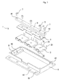
- Fig. 7 is a broken perspective view showing a structure of a semiconductor device according to Embodiment 3 of this invention.
- Fig. 8 is a perspective view showing a state in which the semiconductor device of Fig. 7 is assembled.
- Components which are the same as those of Embodiment 1 are denoted by the same reference numerals, and descriptions thereof are omitted.
- the semiconductor module 2 and a plate-like spring 300 fixed to the upper surface of the semiconductor module 2 are disposed below a beam part 601 formed integrally with a frame part 600 and serving as the reinforcing beam.
- the screw 5 serving as the first fixing tool is fastened as being inserted from below the semiconductor module 2 into the through-hole 24 provided at the central part of the semiconductor module 2, a hole 301 provided in the plate-like spring 300, and a screw hole 602 provided on the beam part 601 in this order, so that the semiconductor module 2 and the plate-like spring 300 are fixed to the beam part 601 of the frame part 600.
- a rib 603 passing between the semiconductor modules 2 fixed to the beam part 601 is formed on the frame part 600 to support the beam part 601.
- the plate-like spring 300 is divided into three components corresponding to the semiconductor modules 2, so that the plate-like spring 300 is fixed to the beam part 601 while avoiding the rib 603.
- the frame part 600 is integrally formed with the beam part 601 serving as the reinforcing beam in the semiconductor device 1 of Embodiment 3, it is possible to achieve a reduction in number of components and a simplification of the assembly process in addition to the effects same as those of the above-described Embodiments. Also, the integrally formed component contributes to realization of a higher rigidity.
- the screw 5 serving as the first fixing tool is inserted from below the semiconductor module 2 to be fastened in the screw hole 602 of the beam part 601, it is unnecessary to provide a screw hole and a nut by insertion molding on the semiconductor module 2. Therefore, thread-cutting on the semiconductor module 2 is unnecessary, and it is possible to prevent rupture of the semiconductor module 2 otherwise caused by a crack or the like in the screw hole.
- a recessed part corresponding to the projecting part of the screw is formed on the cooling member 80 in order to achieve close contact between the cooling member 80 and the semiconductor module 2. Also, as described in Embodiment 1, the structure of fastening from the beam part 601 serving as the reinforcing beam may be adapted.
- the rib 603 is formed on the frame part 600, it is possible to more reliably support the beam part 601, thereby preventing the beam part 601 from being deformed. Accordingly, it is possible to reduce the thickness of the thermally conductive member 82 as well as to suppress the heat resistance, thereby stabilizing the performance of the semiconductor device 1. Note that the rib 603 is not always necessary, and, in the case where the structure wherein the rib 603 is omitted, the shape of the plate-like spring 3 of Embodiment 1 and 2 is adapted without dividing the plate-like spring 300 into three components.
- Embodiment 4 a structure wherein the cooling member 80 attached from the lower surface side of the semiconductor device 1 and the semiconductor module 2 are reliably brought into contact without ensuring the above-specified dimension accuracy will be described.
- Fig. 9 is a sectional view showing a part of the semiconductor device according to Embodiment 4 of this invention, wherein a frame part is omitted.
- Embodiment 4 Since the basic structure of Embodiment 4 is the same as that of Embodiment 1, the perspective view thereof is the same as Fig. 2 . As shown in Fig. 9 , the semiconductor module 2 and the reinforcing beam 4 are fixed via the plate-like spring 3 in a state where the semiconductor module 2 and the plate-like spring 3 arc not in close contact with a slight gap being defined therebetween. Components which are the same as those of Embodiment 1 are denoted by the same reference numerals, and descriptions thereof are omitted.
- the semiconductor module 2 is provided with the control terminal 21 connected to the control unit 83 (see Fig. 4 ) and the terminal 22 for connection to the connection terminal 66a of the frame part 6, and horizontal members 21a and 22b are provided on the control terminal 21 and the terminal 22, respectively.
- a screw hole 230 for fixing the plate-like spring 3 and the reinforcing beam 4 is provided on the central part of the semiconductor module 2, and the screw hole 230 does not penetrate through the semiconductor module 2 to serve as a blind hole.
- the screw hole 230 may be formed by a mold resin, but a structure of allowing insertion molding of the nut 24 is adapted in Embodiment 4 to achieve strengthening of a part of the screw hole 230.
- the screw 5 inserted from above the reinforcing beam 4 is stopped at the bottom of the screw hole 230, so that the plate-like spring 3 and the semiconductor module 2 are fixed with the gap being defined therebetween.
- the lower surface of the semiconductor module 2 is projecting from the lower surface of the frame part 6 by the gap.
- the cooling member 80 is attached to the semiconductor device 1 from below (see Fig. 4 )
- the plate-like member 3 is deformed as being pressed by the cooling member 80, and the lower surface of the semiconductor 2 is moved as being pressed upward by the cooling member 80 to reach the position at which the lower surface of the semiconductor module 2 is on the plane where the lower surface of the frame part 6 is positioned.
- the semiconductor module 2 and the cooling member 80 are reliably brought into contact to each other, and it is possible to keep the small thickness of the thermally conductive member 82 disposed between the semiconductor module 2 and the cooling member 80 as well as to have the thermally conductive member 82 pressed uniformly.
- a projection amount of the semiconductor module 2 may preferably be about 0.05 to 0.2 mm so as not to prevent downsizing of the semiconductor device 1.
- the semiconductor module 2 and the reinforcing beam 4 are fixed in a state where the gap is defined between the semiconductor module 2 and the plate-like spring 3 in the semiconductor device 1 of Embodiment 4, it is possible to change the height of the lower surface of the semiconductor module 2 by way of the deformation of the plate-like spring 3. Accordingly, in the case of fixing the cooling member 80 to the semiconductor device 1, it is possible to align the lower surface of the semiconductor module 2 and the lower surface of the frame part 6 since the semiconductor module 2 is lifted upward as being pressed by the cooling member 80.
- the semiconductor module 2 and the cooling member 80 are brought into contact with each other, and it is possible to keep the small thickness of the thermally conductive member 82 as well as to have the thermally conductive member 82 pressed uniformly.
- the horizontal member 21a and the horizontal member 22a are provided on the control terminal 21 and the terminal 22, respectively, it is possible to alleviate the stress on the connection parts between the control unit 83 and the control terminal 21 and between the connection terminal 66a and the terminal 22 occuring by movement of the semiconductor module 2.
- Embodiment 4 has been described based on the structure of Embodiment 1, it is of course possible to combine the features of Embodiment 4 with the structure of Embodiment 2 or 3. For instance, it is possible to change the through-hole 24 of the semiconductor module 2 into a blind hole in Embodiment 3.
Landscapes
- Physics & Mathematics (AREA)
- Engineering & Computer Science (AREA)
- Microelectronics & Electronic Packaging (AREA)
- Condensed Matter Physics & Semiconductors (AREA)
- General Physics & Mathematics (AREA)
- Computer Hardware Design (AREA)
- Power Engineering (AREA)
- Thermal Sciences (AREA)
- Cooling Or The Like Of Semiconductors Or Solid State Devices (AREA)
Abstract
Description
- This invention relates to a semiconductor device provided with a semiconductor module that is mounted on a mobile object such as a vehicle, the invention contributing particularly to a reduction in influence of a thermal stress due to heating.
- A conventional semiconductor device is generally provided with a semiconductor module having a semiconductor element sealed with a resin and a screw through-hole provided at a central part thereof, a plate-like presser spring disposed at one side of the semiconductor module, a reinforcing beam for reinforcing the presser plate-like spring, and a heatsink disposed at the other side of the semiconductor module, wherein the semiconductor module is fixed to the heatsink by a screw inserted from the reinforcing beam side into the screw through-hole of the semiconductor module via the reinforcing beam and the presser plate-like spring, and the presser plate-like spring has a slit formed for dividing a peripheral part thereof (see
Patent Publication 1, for example). - Patent Publication 1:
JP-A-2005-235 992 Fig. 1 , etc.) - The conventional semiconductor device is formed by fixing the members such as the semiconductor module, the plate-like spring, and the reinforcing beam to the heatsink. The heat generated in the semiconductor module is discharged to the heatsink, and the heat transferred to the heatsink is discharged to the outside via a cooling member attached to a reverse surface (a surface reverse to a surface on which the semiconductor module is attached).
- With such a structure, a thermally conductive member in the form of a paste or a flexible sheet is generally provided between the semiconductor module and the heatsink and between the heatsink and the cooling member for suppressing heat resistance. In order to realize effective thermal conduction by the thermally conductive member, it is necessary to reduce a thickness of the thermally conductive member disposed between the heatsink and the semiconductor module and between the heatsink and the cooling member by increasing a pressure contact force between the members as well as to increase flatness of the heatsink for maintaining uniformity of the thickness. Therefore, a member for forming the heatsink is required to have high rigidity capable of enduring the pressure and ensuring the flatness.
- However, since copper that is generally used as a material satisfying the conditions has a high specific gravity and is expensive, there has been a problem of difficulty in achieving downsizing, light weight, and low cost of the semiconductor device when the copper is used as the member for the heatsink or the rigidity is increased by increasing the thickness of the member. Also, since a plate material that is easily available is generally used in the case of using the copper, there has been a problem of difficulty in shaping from the reasons such as cost suppression in mechanical processing and the like.
- Further, there has been a problem that it is difficult to achieve a reduced and uniform thickness of the thermally conductive member due to reduction of rigidity of the heatsink and deformation of the heatsink that is caused when the heatsink is reduced in thickness, weight, and so forth in order to achieve downsizing, light weight, and reduced cost of the semiconductor device.
- Also, there has been a problem that the semiconductor device has a difficulty in stably exhibiting the original performance since the deformation of the heatsink is subject to various factors such as influences of the pressing force by the reinforcing beam and the plate-like spring, influence of the pressure contact force for keeping the thermally conductive member thin and uniform, and influence of the thermal stress caused by a use environment temperature of the semiconductor device and the heat generation in the semiconductor module.
- The present invention has been made to solve the above-described problems, and an object thereof is to obtain a semiconductor device that is reduced in size, weight, and cost and improved in performance stability and productivity.
- The semiconductor device of this invention comprises: a semiconductor module in which a semiconductor element is sealed with a resin; a reinforcing beam fixed to an upper surface of the semiconductor module; and a frame part to which the reinforcing beam is fixed, the frame part being disposed in such a fashion as to enclose an outer periphery of the semiconductor module and the reinforcing beam fixed to the semiconductor module.
- According to the semiconductor device of this invention, since the semiconductor module is fixed at the frame part by the reinforcing beam, any heatsink is unnecessary, thereby achieving the desired reductions in size, weight, and cost of the semiconductor device. Also, since a heatsink is unnecessary, it is possible to discharge heat generated in the semiconductor module directly to a cooling member as well as to suppress thermal resistance, thereby enabling the semiconductor to stably exhibit its performance.
- The foregoing and other objects, features, aspects, and advantages of the present invention will become more apparent from the following detailed description when read in conjunction with the accompanying drawings.
-
- Fig. 1
- is a broken perspective view showing a structure of a semiconductor device according to
Embodiment 1 of this invention; - Fig. 2
- is a perspective view showing a state in which the semiconductor device of
Fig. 1 is assembled; - Fig. 3
- is a sectional view showing a part of the semiconductor device of
Fig. 2 , wherein a frame part is omitted; - Fig. 4
- is a schematic diagram showing one example of fixing a cooling member and a control unit to the semiconductor device of
Fig. 2 ; - Fig. 5
- is a broken perspective view showing a structure of a semiconductor device according to
Embodiment 2 of this invention; - Fig. 6
- is a perspective view showing a state in which the semiconductor device of
Fig. 5 is assembled; - Fig. 7
- is a broken perspective view showing a structure of a semiconductor device according to
Embodiment 3 of this invention; - Fig. 8
- is a perspective view showing a state in which the semiconductor device of
Fig. 7 is assembled; and - Fig. 9
- is a sectional view showing a part of the semiconductor device according to
Embodiment 4 of this invention, wherein a frame part is omitted. -
Fig. 1 is a broken perspective view showing a structure of a semiconductor device according toEmbodiment 1 of this invention.Fig. 2 is a perspective view showing a state in which the semiconductor device ofFig. 1 is assembled.Fig. 3 is a sectional view showing a part of the semiconductor device ofFig. 2 , wherein a frame part is omitted.Fig. 4 is a schematic diagram showing one example of fixing a cooling member and a control unit to the semiconductor device ofFig. 2 . - Referring to
Figs. 1 to 3 , asemiconductor device 1 is provided withsemiconductor modules 2 in which semiconductor elements are sealed with a resin, a reinforcingbeam 4 fixed to an upper surface of thesemiconductor module 2 via a plate-like spring 3, aframe part 6 disposed in such a fashion as to enclose thesemiconductor module 2, the plate-like spring 3, and the reinforcingbeam 4, the reinforcingbeam 4 having its both ends fixed to theframe part 6. - The
semiconductor modules 2 are provided withcontrol terminals 21 connected to a control unit described later in this specification andterminals 22 for connection to connection terminals that are provided at the frame part and described later in this specification. At a central part of thesemiconductor module 2, ascrew hole 23 is provided for fixing the plate-like spring 3 and the reinforcingbeam 4. - In
Embodiment 1, threesemiconductor modules 2 are disposed in line at a predetermined interval, and the plate-like spring 3 of which a part at a position corresponding to each of thesemiconductor modules 2 is formed into a pentroof type sectional shape is disposed on the upper surface of each of thesemiconductor modules 2. Also, afixing hole 31 is provided at a position on the plate-like spring 3 corresponding to thescrew hole 23 of thesemiconductor module 2. - On an upper surface of the plate-
like spring 3, thereinforcing beam 4 extending in a direction in which thesemiconductor modules 2 are disposed, i.e. along a length direction of the plate-like spring 3, is disposed, and through-holes 41 are provided corresponding to the interval at which the threesemiconductor modules 2 are disposed. Afixing hole 42 for the fixation to theframe part 6 is provided at each of the both ends of the reinforcingbeam 4. - The reinforcing
beam 4, the plate-like spring 3, and thesemiconductor modules 2 are fixed to one another by ascrew 5 inserted as a first fastening tool from above the reinforcingbeam 4 into the through-hole 41, thehole 31, and thescrew hole 23 in this order. - For example, it is possible to directly fix the reinforcing
beam 4 and thesemiconductor module 2 to each other without the plate-like spring 3. However, due to the structure of fixing with the plate-like spring 3 being placed between thereinforcing beam 4 and thesemiconductor module 2 as inEmbodiment 1, the fastening force of thescrew 5 is distributed by flexure of a part of the pentroof type sectional shape of the plate-like spring 3, so that a uniform load is applied on thesemiconductor module 2 when the plate-like spring 3 is fixed as being perfectly spread. - Though the members are fixed by providing the
screw hole 23 formed from a mold resin on thesemiconductor module 2 and fastening thescrew 5 inserted from the side of the reinforcingbeam 4 to thesemiconductor module 2 inEmbodiment 1, a nut may be formed inside thesemiconductor module 2 by insertion molding when there is a risk of cracking in the resin or when a high fastening force is required. - Also, the fixing method is not limited to the above, and the members may be fixed by providing a through-hole in the
semiconductor module 2 in place of thescrew hole 23, disposing a nut on a lower surface of thesemiconductor module 2, and fastening thescrew 5 with the nut, for example. - Furthermore, the members may be fixed by providing a through-hole in the
semiconductor module 2 in place of thescrew hole 23, providing a screw hole in the reinforcingbeam 4 in place of the through-hole 41, and inserting the screw from the lower surface of thesemiconductor module 2. With such constitution, thread-cutting on thesemiconductor module 2 is unnecessary, and it is possible to prevent rupture of thesemiconductor module 2 otherwise caused by a crack or the like in thescrew hole 23. - The
frame part 6 is formed in the form of a frame in such a fashion as to enclose from four directions thereinforcing beam 4, the plate-like spring 3, and thesemiconductor module 2 that are integrally fixed to one another. Astep part 61 is projecting from each of opposite inner walls in a width direction of theframe part 6 for fixing the reinforcingbeam 4, and ascrew hole 62 is provided at a central part of thestep part 61. - The reinforcing
beam 4 is disposed in such a fashion that thefixing hole 42 of the reinforcingbeam 4 overlaps with thescrew hole 62, so that the reinforcingbeam 4 and theframe part 6 are fixed to each other when ascrew 7 serving as a second fixing tool is inserted from the side of the reinforcingbeam 4 to be fastened in thescrew hole 62. - Thus, the
semiconductor module 2, the plate-like spring 3, thereinforcing beam 4, and theframe part 6 are integrally fixed to form thesemiconductor device 1. Though only thereinforcing beam 4 is fixed to theframe part 6 inEmbodiment 1, this invention is not limited thereto, and the plate-like spring 3 may be fixed to theframe part 6 together with thereinforcing beam 4 by extending both ends in the length direction of the plate-like spring 3. - Jutting
parts 64 in which fixing holes 63 for fixing onto the cooling member described later in this specification are disposed are formed on each of both outer wall surfaces in the length direction of theframe part 6.Support parts 65 for fixing and supporting the control unit described later in this specification are provided at each of four corners of an upper surface of a framing part of theframe part 6. - A thermoplastic synthetic resin material such as ABS, PBT, and PPS may be used as a material for the
frame part 6, and theframe part 6 may be shaped by injection molding. A plurality ofbus bars 66 that are made from a metal having a high electroconductivity, such as copper, are formed inside theframe part 6 by insertion molding or the like to serve as conductors. - One end of the
bus bar 66 is exposed to an inner wall side of theframe part 6 as aconnection terminal 66a to be connected to theterminal 22 of thesemiconductor module 2, and the other end is exposed to an outer wall side of theframe part 6 as anexternal terminal 66b to be connected to an external component. The terminal 22 and theconnection terminal 66a are connected by welding, for example, to form a desired electric circuit. Of course, the connection method is not limited to the welding, and the connection may be established by fastening with a screw. - In
Embodiment 1, thicknesses of thesemiconductor module 2, theframe part 6, thestep part 61, and the like are so set that positions of the lower surface of thesemiconductor module 2 and the lower surface of theframe part 6 are on an identical plane when the members (semiconductor module 2, plate-like spring 3, reinforcingbeam 4, frame part 6) are integrally fixed. With such a constitution, the cooling member described later in this specification and the lower surface of thesemiconductor module 2 are reliably brought into contact with each other. - Hereinafter, one example of fixing the cooling
member 80 and thecontrol unit 83 to thesemiconductor device 1 having the structure described above will be described with reference toFig. 4 . The schematic diagram ofFig. 4 is a diagram as viewed from a side of thesemiconductor device 1 shown inFig. 2 in the width direction. - As shown in
Fig. 4 , the coolingmember 80 is disposed at a side of the lower surface of thesemiconductor device 1 and used for discharging heat generated in thesemiconductor module 2 by contacting the lower surface of thesemiconductor module 2. For example, ascrew hole 81 is provided on the coolingmember 80 at a position corresponding to the fixinghole 63 provided on the respective juttingpart 64 of theframe part 6. - The cooling
member 80 is disposed below theframe part 6 in such a fashion as to be in contact with the lower surface of thesemiconductor module 2, and a screw is fastened in thescrew hole 81 of the coolingmember 80 via the fixinghole 63, so that theframe part 6 and the coolingmember 80 are fixed to each other. The fixing method of theframe member 6 and the coolingmember 80 is not limited to the above, and theframe member 6 and the coolingmember 80 are fixed in accordance with use conditions and the like of thesemiconductor device 1. - A thermally conductive member 82 (see
Fig. 4 ) having a thermal conductivity ratio of about 1 W/mK to several W/mK and in the form of a paste or a flexible sheet is provided between thesemiconductor module 2 and the coolingmember 80 by coating, sandwiching, or the like. The thermallyconductive member 82 allows smooth thermal conduction by closely contacting a contact surface between thesemiconductor module 2 and the coolingmember 80. A heat discharge effect of the thermallyconductive member 82 is increased as the thickness thereof is reduced, but heat resistance of a part having a relatively large thickness is increased when the thickness is increased and non-uniform. - Since performance of the thermally
conducive member 82 is limited to the part having the larger heat resistance, the thermallyconductive member 82 can be the major factor of deterioration of heat resistance when the thermallyconductive member 82 is not used appropriately. Therefore, it is desirable to keep the thickness of the thermallyconductive member 82 small and uniform by increasing a pressure contact force between thesemiconductor module 2 and the coolingmember 80. - Since the
semiconductor module 2 is fixed to theframe part 6 by the reinforcingbeam 4 inEmbodiment 1, the pressure contact force depends on rigidity of the reinforcingbeam 4. Therefore, by using an iron-based material having a high Young's modulus as a material for the reinforcingbeam 4, it is possible to more reliably prevent the reinforcingbeam 4 from being deformed and the like when the pressure contact force is increased. - Though only the both ends of the reinforcing
beam 4 are fixed to theframe part 6 inEmbodiment 1, a rib, for example, passing between thesemiconductor modules 2 may be provided in the length direction of theframe part 6 for further suppressing the reinforcingbeam 4 from being deformed. By fixing the both ends of the reinforcingbeam 4 not only to theframe part 6 but also to the rib, it is possible to further suppress the reinforcingbeam 4 from being deformed. - Also, a force of pressing the
central semiconductor module 2 among the threesemiconductor modules 2 can be weakened as compared to those of thesemiconductor modules 2 on both ends when the reinforcingbeam 4 is slightly deformed depending on the rigidity of the reinforcingbeam 4. - In such case, it is possible to reinforce the pressing force for the
central semiconductor module 2 by changing the deformation amount of the central spring at a part of the pentroof type sectional shape among the plate-like springs 3. Specifically, the deformation amount of the spring is increased by increasing an angle of an inclined part of the pentroof type section, thereby increasing the pressing force for thesemiconductor module 2. Also, the deformation amount of the spring may be changed by changing a spring constant of the plate-like spring 3. - In the case of fixing the reinforcing
beam 4, the plate-like spring 3, and thesemiconductor module 2 by providing the through-hole in thesemiconductor module 2 and disposing the nut on the lower surface side of thesemiconductor module 2 or by providing the through-hole in thesemiconductor module 2, providing the screw hole in the reinforcingbeam 4, and inserting the screw from the lower surface side of thesemiconductor module 2, head portions of the nut and the screw are projecting on the lower surface of thesemiconductor module 2. - Therefore, in order to achieve the close contact between the cooling
member 80 and thesemiconductor module 2, a recessed part is provided on the coolingmember 80 at a part corresponding to the jutting part of the nut. - The control unit 83 (see
Fig. 4 ) is disposed above theframe part 6, for example, for driving and controlling thesemiconductor module 2. InEmbodiment 1, through-holes 84 are provided in thecontrol unit 83 at each of positions corresponding to thesupport members 65 provided at the four corners of the framing part of theframe part 6, and thecontrol unit 83 is fastened with a screw as being disposed in such a fashion as to cover the upper side of theframe part 6, thereby fixing thecontrol unit 83 and theframe part 6 to each other. - By connecting the
control terminal 21 of thesemiconductor module 2 to thecontrol unit 83, thecontrol unit 83 performs the control on thesemiconductor module 2. Of course, the connection method for theframe part 6 and thecontrol unit 83 is not limited to the above, and the fixing method may be selected in accordance with use conditions and the like of thesemiconductor device 1. - As described in the foregoing, since the
semiconductor device 1 ofEmbodiment 1 does not require the heatsink since thesemiconductor module 2 is fixed to theframe part 6 via the reinforcingbeam 4, reductions in size, weight, and cost of thesemiconductor device 1 are achieved. - Also, since the heatsink is not provided, it is possible to discharge the heat of the
semiconductor module 2 by bringing thesemiconductor module 2 and the coolingmember 80 into direct contact with each other as well as to reduce the number of the thermallyconductive member 82 worsening the heat resistance provided between thesemiconductor module 2 and the coolingmember 80 to only one. - Accordingly, since the heat resistance is suppressed and the heat generated in the
semiconductor module 2 is effectively discharged, performance of thesemiconductor device 1 is stably exhibited. Also, due to the reduction in number of components, it is possible to achieve a reduced cost, a reduction in assembly process steps, and improvement in productivity. - Also, by forming the reinforcing
beam 4 from the material having the high rigidity, it is possible to prevent the reinforcingbeam 4 from being deformed when the pressure contact force between thesemiconductor module 2 and the coolingmember 80 is increased. Accordingly, it is possible to reliably establish the pressure contact between the upper surface of the coolingmember 80 disposed at the lower surface side of theframe 6 and the lower surface of thesemiconductor module 2 as well as to keep the thickness of the thermallyconductive member 82 disposed between the members to be small and uniform. Therefore, the heat resistance is suppressed, thereby stabilizing the performance of thesemiconductor device 1. - Since the fastening force of the
screw 5 is distributed when the part of the pentroof type sectional shape of the plate-like spring 3 is deflected by fixing thesemiconductor module 2 and the reinforcingbeam 4 to each other via the plate-like spring 3, it is possible to uniformly apply a load on thewhole semiconctor modules 2. - It is possible to adjust the pressing force for the
semiconctor module 2 by partially changing the spring deformation amount of the plate-like spring 3. For example, by increasing the spring deformation amount of the part of the pentroof type sectional shape positioned at the central part of the plate-like spring 3 where the reinforcingbeam 4 is subject to deformation, it is possible to reinforce the pressing force for thecentral semiconductor module 2, thereby keeping the uniform pressure contact force between thesemiconductor module 2 and the coolingmember 80. - Since a synthetic resin is used as the material for the
frame part 6, and since the plurality ofbus bars 66 are formed inside theframe part 6 by insertion molding, wiring work and connection work inside thesemiconductor device 1 are facilitated, and it is possible to realize a preferable shape of thesemiconductor device 1 easily and at a low cost. - Since the
support part 65 for supporting thecontrol unit 83 that controls thesemiconductor module 2 is provided on theframe part 6, it is possible to support thecontrol unit 83 by a simple structure, thereby enabling a reduction in number of components, suppression of assembly cost, simplification of assembly process, and improvement in productivity. - While the
frame part 6 is made from a synthetic resin material inEmbodiment 1, the frame part is made from a metal having high rigidity inEmbodiment 2.Fig. 5 is a broken perspective view showing a structure of a semiconductor device according toEmbodiment 2 of this invention.Fig. 6 is a perspective view showing a state in which the semiconductor device ofFig. 5 is assembled. Components which are the same as those ofEmbodiment 1 are denoted by the same reference numerals, and descriptions thereof are omitted. - Referring to
Figs. 5 and6 , aframe part 6 is made from a metal material having high rigidity, such as iron, aluminum, and magnesium, and produced by molding, die casting, or the like. Since theframe part 6 itself is formed from an electroconductive material, it is difficult to adapt the structure ofEmbodiment 1 wherein the bus bars serving as electroconductive parts are formed by insertion molding, and the connection terminal and the external terminal are exposed. Accordingly, a terminal board (not shown) for forming internal wiring and external terminal is separately provided. - As described above, since the
frame part 6 is a molded article, die cast article, or the like made from the metal material having a greater freedom degree for shaping in thesemiconductor device 1 ofEmbodiment 2, it is possible to enable improvement in rigidity in the frame part, easy shaping, and low production cost in addition to the effects ofEmbodiment 1. - Since the
support member 65 supporting thecontrol unit 83 is also made from the metal material, the rigidity in increased, and it is possible to prevent a loss at thesupport part 65 otherwise caused by vibration of thesemiconductor device 1, thereby improving vibration resistance of thesemiconductor device 1. - Also, when a rib (not shown) passing between the
semiconductor modules 2 and made from the metal material is provided on theframe part 6, it is possible to further suppress the reinforcingbeam 4 from being deformed as compared toEmbodiment 1 as well as to reliably achieve reductions in thickness and heat resistance of the thermallyconductive member 82. - While the frame part and the reinforcing beam are formed as separate components and fixed by a screw and the like in
Embodiments Embodiment 3. A material for the frame part may be a synthetic resin as inEmbodiment 1 or a metal material as inEmbodiment 2 depending on the object, and the case of using a metal material will be described inEmbodiment 3. -
Fig. 7 is a broken perspective view showing a structure of a semiconductor device according toEmbodiment 3 of this invention.Fig. 8 is a perspective view showing a state in which the semiconductor device ofFig. 7 is assembled. Components which are the same as those ofEmbodiment 1 are denoted by the same reference numerals, and descriptions thereof are omitted. - As shown in
Figs. 7 and8 , thesemiconductor module 2 and a plate-like spring 300 fixed to the upper surface of thesemiconductor module 2 are disposed below abeam part 601 formed integrally with aframe part 600 and serving as the reinforcing beam. - The
screw 5 serving as the first fixing tool is fastened as being inserted from below thesemiconductor module 2 into the through-hole 24 provided at the central part of thesemiconductor module 2, ahole 301 provided in the plate-like spring 300, and ascrew hole 602 provided on thebeam part 601 in this order, so that thesemiconductor module 2 and the plate-like spring 300 are fixed to thebeam part 601 of theframe part 600. - A
rib 603 passing between thesemiconductor modules 2 fixed to thebeam part 601 is formed on theframe part 600 to support thebeam part 601. The plate-like spring 300 is divided into three components corresponding to thesemiconductor modules 2, so that the plate-like spring 300 is fixed to thebeam part 601 while avoiding therib 603. - Since the
frame part 600 is integrally formed with thebeam part 601 serving as the reinforcing beam in thesemiconductor device 1 ofEmbodiment 3, it is possible to achieve a reduction in number of components and a simplification of the assembly process in addition to the effects same as those of the above-described Embodiments. Also, the integrally formed component contributes to realization of a higher rigidity. - Since the
screw 5 serving as the first fixing tool is inserted from below thesemiconductor module 2 to be fastened in thescrew hole 602 of thebeam part 601, it is unnecessary to provide a screw hole and a nut by insertion molding on thesemiconductor module 2. Therefore, thread-cutting on thesemiconductor module 2 is unnecessary, and it is possible to prevent rupture of thesemiconductor module 2 otherwise caused by a crack or the like in the screw hole. - In the case where a head portion of the
screw 5 is projecting on the lower surface of thesemiconductor module 2, a recessed part corresponding to the projecting part of the screw is formed on the coolingmember 80 in order to achieve close contact between the coolingmember 80 and thesemiconductor module 2. Also, as described inEmbodiment 1, the structure of fastening from thebeam part 601 serving as the reinforcing beam may be adapted. - Since the
rib 603 is formed on theframe part 600, it is possible to more reliably support thebeam part 601, thereby preventing thebeam part 601 from being deformed. Accordingly, it is possible to reduce the thickness of the thermallyconductive member 82 as well as to suppress the heat resistance, thereby stabilizing the performance of thesemiconductor device 1. Note that therib 603 is not always necessary, and, in the case where the structure wherein therib 603 is omitted, the shape of the plate-like spring 3 ofEmbodiment like spring 300 into three components. - While the lower surface of the
semiconductor module 2 and the lower surface of the frame part 6 (frame part 600) are positioned on the identical plane in thesemiconductor device 1 described inEmbodiments 1 to 3, so that the coolingmember 80 attached from the lower surface side of thesemiconductor device 1 and thesemiconductor module 2 are brought into contact without fail, and that the thermallyconductive member 82 disposed between the coolingmember 80 and thesemiconductor module 2 is thin and uniformly pressed. - As accuracy is required for such a design, it is necessary to keep a difference between the lower surface of the
semiconductor module 2 and the lower surface of theframe part 6 to be ± 50 µm or less. Therefore, it is generally considered desirable to perform molding of thesemiconductor module 2, the frame part 6 (frame part 600), and the like with accuracy achieving the accuracy of ± 50 µm or less. - In
Embodiment 4, a structure wherein the coolingmember 80 attached from the lower surface side of thesemiconductor device 1 and thesemiconductor module 2 are reliably brought into contact without ensuring the above-specified dimension accuracy will be described. -
Fig. 9 is a sectional view showing a part of the semiconductor device according toEmbodiment 4 of this invention, wherein a frame part is omitted. - Since the basic structure of
Embodiment 4 is the same as that ofEmbodiment 1, the perspective view thereof is the same asFig. 2 . As shown inFig. 9 , thesemiconductor module 2 and the reinforcingbeam 4 are fixed via the plate-like spring 3 in a state where thesemiconductor module 2 and the plate-like spring 3 arc not in close contact with a slight gap being defined therebetween. Components which are the same as those ofEmbodiment 1 are denoted by the same reference numerals, and descriptions thereof are omitted. - As shown in
Figs. 2 and9 , thesemiconductor module 2 is provided with thecontrol terminal 21 connected to the control unit 83 (seeFig. 4 ) and the terminal 22 for connection to theconnection terminal 66a of theframe part 6, andhorizontal members 21a and 22b are provided on thecontrol terminal 21 and the terminal 22, respectively. - A
screw hole 230 for fixing the plate-like spring 3 and the reinforcingbeam 4 is provided on the central part of thesemiconductor module 2, and thescrew hole 230 does not penetrate through thesemiconductor module 2 to serve as a blind hole. Thescrew hole 230 may be formed by a mold resin, but a structure of allowing insertion molding of thenut 24 is adapted inEmbodiment 4 to achieve strengthening of a part of thescrew hole 230. - In the case of fixing the reinforcing
beam 4, the plate-like spring 3, and thesemiconductor module 2, thescrew 5 inserted from above the reinforcingbeam 4 is stopped at the bottom of thescrew hole 230, so that the plate-like spring 3 and thesemiconductor module 2 are fixed with the gap being defined therebetween. - With the structure of defining the gap as described above, when the reinforcing
beam 4 is fixed to theframe part 6 to integrally fix thesemiconductor module 2, the plate-like spring 3, the reinforcingbeam 4, and theframe part 6, the lower surface of thesemiconductor module 2 is projecting from the lower surface of theframe part 6 by the gap. When the coolingmember 80 is attached to thesemiconductor device 1 from below (seeFig. 4 ), the plate-like member 3 is deformed as being pressed by the coolingmember 80, and the lower surface of thesemiconductor 2 is moved as being pressed upward by the coolingmember 80 to reach the position at which the lower surface of thesemiconductor module 2 is on the plane where the lower surface of theframe part 6 is positioned. - Therefore, even when the dimension accuracy in a thickness direction of the
semiconductor module 2 and theframe part 6 is not maintained as high as specified above, thesemiconductor module 2 and the coolingmember 80 are reliably brought into contact to each other, and it is possible to keep the small thickness of the thermallyconductive member 82 disposed between thesemiconductor module 2 and the coolingmember 80 as well as to have the thermallyconductive member 82 pressed uniformly. - When the
semiconductor module 2 is moved as being pressed upward by the coolingmember 80, relative positions of thesemiconductor module 2 and theframe part 6 are changed to easily cause a stress on the connection part of thecontrol unit 83 and thecontrol terminal 21 and the connection part of theconnection terminal 66a and the terminal 22. In such a case, the stress caused on the connection parts is alleviated by deformation of thehorizontal parts control terminal 21 and the terminal 22. - Since the stress applied on the connection parts is increased in the case where the
semiconductor module 2 is greatly projecting as compared to theframe 6, i.e. in the case where the gap between thesemiconductor module 2 and the plate-like spring 3 is large, it is necessary to lengthen thehorizontal parts semiconductor module 2 may preferably be about 0.05 to 0.2 mm so as not to prevent downsizing of thesemiconductor device 1. - Since the
semiconductor module 2 and the reinforcingbeam 4 are fixed in a state where the gap is defined between thesemiconductor module 2 and the plate-like spring 3 in thesemiconductor device 1 ofEmbodiment 4, it is possible to change the height of the lower surface of thesemiconductor module 2 by way of the deformation of the plate-like spring 3. Accordingly, in the case of fixing the coolingmember 80 to thesemiconductor device 1, it is possible to align the lower surface of thesemiconductor module 2 and the lower surface of theframe part 6 since thesemiconductor module 2 is lifted upward as being pressed by the coolingmember 80. - Therefore, without ensuring the dimension accuracy in the thickness direction of the
semiconductor module 2 and theframe part 6 as high as the above-specified accuracy, thesemiconductor module 2 and the coolingmember 80 are brought into contact with each other, and it is possible to keep the small thickness of the thermallyconductive member 82 as well as to have the thermallyconductive member 82 pressed uniformly. - Since the
horizontal member 21a and thehorizontal member 22a are provided on thecontrol terminal 21 and the terminal 22, respectively, it is possible to alleviate the stress on the connection parts between thecontrol unit 83 and thecontrol terminal 21 and between theconnection terminal 66a and the terminal 22 occuring by movement of thesemiconductor module 2. - Though
Embodiment 4 has been described based on the structure ofEmbodiment 1, it is of course possible to combine the features ofEmbodiment 4 with the structure ofEmbodiment hole 24 of thesemiconductor module 2 into a blind hole inEmbodiment 3. - Various modifications and alterations of this invention will be apparent to those skilled in the art without departing from the scope and spirit of this invention, and it should be understood that this invention is not limited to the illustrative embodiments set forth herein.
Claims (8)
- A semiconductor device (1) comprising:- a semiconductor module (2) in which a semiconductor element is sealed with a resin,- a reinforcing beam (4) fixed to an upper surface of the semiconductor module (2), and- a frame part (6) to which the reinforcing beam (4) is fixed, the frame part (6) being disposed in such a fashion as to enclose an outer periphery of the semiconductor module (2) and the reinforcing beam (4) fixed to the semiconductor module (2).
- The semiconductor device according to claim 1,
wherein the semiconductor module (2) and the reinforcing beam (4) are fixed via a plate-like spring (3). - The semiconductor device according to claim 2,
wherein the semiconductor module (2) and the reinforcing beam (4) are fixed with a gap being defined between the semiconductor module (2) and the plate-like spring (3), and
wherein the semiconductor module (2) is movable in a vertical direction with respect to the frame part (6) by way of deformation of the plate-like spring (3). - The semiconductor device according to claim 2 or 3,
wherein a deformation amount of the plate-like spring (3) is partially changed. - The semiconductor device according to any one of claims 1 to 4,
wherein the frame part (6) is made from a synthetic resin, and
wherein a conduction part (66) electrically connected to the semiconductor module (2) is formed inside the frame part (6) by insertion molding. - The semiconductor device according to any one of claims 1 to 4,
wherein the frame part (6) is made from a metal material. - The semiconductor device according to any one of claims 1 to 6,
wherein the frame part (600) is integrally formed with the reinforcing beam (601). - The semiconductor device according to any one of claims 1 to 7,
wherein the frame part (6) comprises a support member (65) for supporting a control unit (83) controlling the semiconductor module (2).
Applications Claiming Priority (1)
| Application Number | Priority Date | Filing Date | Title |
|---|---|---|---|
| JP2007206163A JP5014016B2 (en) | 2007-08-08 | 2007-08-08 | Semiconductor device |
Publications (3)
| Publication Number | Publication Date |
|---|---|
| EP2023389A2 true EP2023389A2 (en) | 2009-02-11 |
| EP2023389A3 EP2023389A3 (en) | 2013-03-20 |
| EP2023389B1 EP2023389B1 (en) | 2015-01-21 |
Family
ID=40070805
Family Applications (1)
| Application Number | Title | Priority Date | Filing Date |
|---|---|---|---|
| EP08161714.4A Ceased EP2023389B1 (en) | 2007-08-08 | 2008-08-04 | Semiconductor device |
Country Status (5)
| Country | Link |
|---|---|
| US (1) | US7880299B2 (en) |
| EP (1) | EP2023389B1 (en) |
| JP (1) | JP5014016B2 (en) |
| KR (1) | KR100984880B1 (en) |
| CN (1) | CN101364575B (en) |
Cited By (1)
| Publication number | Priority date | Publication date | Assignee | Title |
|---|---|---|---|---|
| EP4164349A1 (en) | 2021-10-06 | 2023-04-12 | MAHLE International GmbH | Control device for an electric machine |
Families Citing this family (20)
| Publication number | Priority date | Publication date | Assignee | Title |
|---|---|---|---|---|
| JP5267283B2 (en) * | 2009-04-02 | 2013-08-21 | 三菱電機株式会社 | Power module |
| DE102009002993B4 (en) * | 2009-05-11 | 2012-10-04 | Infineon Technologies Ag | Power semiconductor module with spaced circuit carriers |
| JP4968316B2 (en) * | 2009-12-14 | 2012-07-04 | アンデン株式会社 | Electronic circuit equipment |
| US8198725B2 (en) * | 2009-12-31 | 2012-06-12 | Star Technologies Inc. | Heat sink and integrated circuit assembly using the same |
| JP2012054262A (en) * | 2010-08-31 | 2012-03-15 | Mitsubishi Electric Corp | Semiconductor device |
| JP5510432B2 (en) * | 2011-02-28 | 2014-06-04 | 株式会社豊田自動織機 | Semiconductor device |
| JP5832215B2 (en) * | 2011-09-28 | 2015-12-16 | 株式会社ケーヒン | Semiconductor control device |
| KR101228841B1 (en) * | 2011-10-04 | 2013-02-04 | 엘에스산전 주식회사 | A springy clip type apparatus for fastening power semiconductor |
| JP5971190B2 (en) * | 2012-06-07 | 2016-08-17 | 株式会社豊田自動織機 | Semiconductor device |
| JP2014064463A (en) * | 2013-12-20 | 2014-04-10 | Panasonic Corp | Power supply control device |
| JP6645315B2 (en) * | 2016-03-29 | 2020-02-14 | アイシン・エィ・ダブリュ株式会社 | Inverter device and method of manufacturing inverter device |
| JP6920790B2 (en) * | 2016-05-24 | 2021-08-18 | ローム株式会社 | How to assemble intelligent power modules, electric or hybrid vehicles, and intelligent power modules |
| JP6800319B2 (en) * | 2017-04-21 | 2020-12-16 | 三菱電機株式会社 | Power converter |
| WO2019215805A1 (en) * | 2018-05-08 | 2019-11-14 | 三菱電機株式会社 | Fastening structure and power conversion device using fastening structure |
| DE102019122640A1 (en) * | 2019-08-22 | 2021-02-25 | Ebm-Papst Mulfingen Gmbh & Co. Kg | Holding device for thermal contact between an electronic component mounted on a printed circuit board and a heat sink |
| CN111225544B (en) * | 2019-12-06 | 2021-11-05 | 法雷奥西门子新能源汽车(深圳)有限公司 | Heat sink for electronic component |
| US11444002B2 (en) * | 2020-07-29 | 2022-09-13 | Taiwan Semiconductor Manufacturing Company, Ltd. | Package structure |
| JP7452373B2 (en) * | 2020-10-19 | 2024-03-19 | 株式会社デンソー | power converter |
| JP7468433B2 (en) | 2021-03-30 | 2024-04-16 | 株式会社豊田自動織機 | Electric Compressor |
| JP2023009908A (en) * | 2021-07-08 | 2023-01-20 | 株式会社豊田自動織機 | electric compressor |
Citations (2)
| Publication number | Priority date | Publication date | Assignee | Title |
|---|---|---|---|---|
| JP2005235992A (en) | 2004-02-19 | 2005-09-02 | Mitsubishi Electric Corp | Semiconductor apparatus |
| US20070008700A1 (en) | 2005-07-05 | 2007-01-11 | Cheng-Ping Lee | Power supply with heat sink |
Family Cites Families (10)
| Publication number | Priority date | Publication date | Assignee | Title |
|---|---|---|---|---|
| JPS6223079Y2 (en) * | 1981-01-27 | 1987-06-12 | ||
| JPH0289356A (en) * | 1988-09-26 | 1990-03-29 | Mitsubishi Electric Corp | Semiconductor device |
| JPH02140856U (en) * | 1989-04-27 | 1990-11-26 | ||
| US6043981A (en) * | 1997-11-13 | 2000-03-28 | Chrysler Corporation | Heat sink assembly for electrical components |
| US5977640A (en) * | 1998-06-26 | 1999-11-02 | International Business Machines Corporation | Highly integrated chip-on-chip packaging |
| JP2001160696A (en) | 1999-12-02 | 2001-06-12 | Kenwood Corp | Electronic component mounting mechanism |
| JP3881488B2 (en) * | 1999-12-13 | 2007-02-14 | 株式会社東芝 | Circuit module cooling device and electronic apparatus having the cooling device |
| JP3725103B2 (en) * | 2002-08-23 | 2005-12-07 | 三菱電機株式会社 | Semiconductor device |
| DE102005055713B4 (en) * | 2005-11-23 | 2011-11-17 | Semikron Elektronik Gmbh & Co. Kg | Power semiconductor module with connection elements |
| JP4589239B2 (en) * | 2006-01-12 | 2010-12-01 | 株式会社日立製作所 | Electronic equipment cooling structure |
-
2007
- 2007-08-08 JP JP2007206163A patent/JP5014016B2/en active Active
-
2008
- 2008-07-15 US US12/173,495 patent/US7880299B2/en active Active
- 2008-08-04 EP EP08161714.4A patent/EP2023389B1/en not_active Ceased
- 2008-08-07 KR KR1020080077478A patent/KR100984880B1/en active IP Right Grant
- 2008-08-07 CN CN2008101453535A patent/CN101364575B/en active Active
Patent Citations (2)
| Publication number | Priority date | Publication date | Assignee | Title |
|---|---|---|---|---|
| JP2005235992A (en) | 2004-02-19 | 2005-09-02 | Mitsubishi Electric Corp | Semiconductor apparatus |
| US20070008700A1 (en) | 2005-07-05 | 2007-01-11 | Cheng-Ping Lee | Power supply with heat sink |
Cited By (1)
| Publication number | Priority date | Publication date | Assignee | Title |
|---|---|---|---|---|
| EP4164349A1 (en) | 2021-10-06 | 2023-04-12 | MAHLE International GmbH | Control device for an electric machine |
Also Published As
| Publication number | Publication date |
|---|---|
| US20090039504A1 (en) | 2009-02-12 |
| JP5014016B2 (en) | 2012-08-29 |
| JP2009043863A (en) | 2009-02-26 |
| CN101364575B (en) | 2011-10-12 |
| EP2023389B1 (en) | 2015-01-21 |
| KR20090015844A (en) | 2009-02-12 |
| EP2023389A3 (en) | 2013-03-20 |
| US7880299B2 (en) | 2011-02-01 |
| KR100984880B1 (en) | 2010-10-01 |
| CN101364575A (en) | 2009-02-11 |
Similar Documents
| Publication | Publication Date | Title |
|---|---|---|
| EP2023389B1 (en) | Semiconductor device | |
| JP5028085B2 (en) | Electronic circuit device and manufacturing method thereof | |
| JP4936021B2 (en) | Motor control device | |
| US10582607B2 (en) | Circuit assembly having a heat transfer member | |
| US7321492B2 (en) | Heat sink module for an electronic device | |
| JP2013070028A (en) | Electronic controller | |
| JP7016054B2 (en) | Power supplies, headlights, and mobiles | |
| JP4643703B2 (en) | Semiconductor device fixture and mounting structure thereof | |
| US20220263305A1 (en) | Circuit structure | |
| CN115985855A (en) | Power module and method for producing power module | |
| CN211959879U (en) | Thermal interface for multiple discrete electronic devices | |
| JP2008258241A (en) | Semiconductor device | |
| JP2001177280A (en) | Casing for electric device | |
| WO2016113858A1 (en) | Motor, and motor production method | |
| JP2008103577A (en) | Heat dissipating structure for power module, and motor controller equipped with the same | |
| JP4685039B2 (en) | Power semiconductor device | |
| US6535383B2 (en) | Clamshell heatsink | |
| JP7148274B2 (en) | electrical equipment | |
| JP5892691B2 (en) | Electronic equipment | |
| US20060164810A1 (en) | Electronic device comprising secure heat dissipation | |
| JP2007174863A (en) | Busbar connection type electronic circuit device and attaching method therefor | |
| JP4342253B2 (en) | Resin mold electrode | |
| JP2671700B2 (en) | Electrical equipment | |
| JP2018174218A (en) | Fixing structure of heating component and fixing method of heating component | |
| JP5022916B2 (en) | Mounting structure for components that can mount heating elements, metal bodies, and components that can mount heating elements |
Legal Events
| Date | Code | Title | Description |
|---|---|---|---|
| PUAI | Public reference made under article 153(3) epc to a published international application that has entered the european phase |
Free format text: ORIGINAL CODE: 0009012 |
|
| AK | Designated contracting states |
Kind code of ref document: A2 Designated state(s): AT BE BG CH CY CZ DE DK EE ES FI FR GB GR HR HU IE IS IT LI LT LU LV MC MT NL NO PL PT RO SE SI SK TR |
|
| AX | Request for extension of the european patent |
Extension state: AL BA MK RS |
|
| PUAL | Search report despatched |
Free format text: ORIGINAL CODE: 0009013 |
|
| AK | Designated contracting states |
Kind code of ref document: A3 Designated state(s): AT BE BG CH CY CZ DE DK EE ES FI FR GB GR HR HU IE IS IT LI LT LU LV MC MT NL NO PL PT RO SE SI SK TR |
|
| AX | Request for extension of the european patent |
Extension state: AL BA MK RS |
|
| RIC1 | Information provided on ipc code assigned before grant |
Ipc: H05K 7/20 20060101ALI20130208BHEP Ipc: H01L 23/40 20060101AFI20130208BHEP |
|
| 17P | Request for examination filed |
Effective date: 20130730 |
|
| RBV | Designated contracting states (corrected) |
Designated state(s): AT BE BG CH CY CZ DE DK EE ES FI FR GB GR HR HU IE IS IT LI LT LU LV MC MT NL NO PL PT RO SE SI SK TR |
|
| AKX | Designation fees paid |
Designated state(s): DE FR IT |
|
| 17Q | First examination report despatched |
Effective date: 20131105 |
|
| GRAP | Despatch of communication of intention to grant a patent |
Free format text: ORIGINAL CODE: EPIDOSNIGR1 |
|
| INTG | Intention to grant announced |
Effective date: 20140804 |
|
| GRAS | Grant fee paid |
Free format text: ORIGINAL CODE: EPIDOSNIGR3 |
|
| GRAA | (expected) grant |
Free format text: ORIGINAL CODE: 0009210 |
|
| AK | Designated contracting states |
Kind code of ref document: B1 Designated state(s): DE FR IT |
|
| REG | Reference to a national code |
Ref country code: DE Ref legal event code: R096 Ref document number: 602008036428 Country of ref document: DE Effective date: 20150305 |
|
| REG | Reference to a national code |
Ref country code: DE Ref legal event code: R097 Ref document number: 602008036428 Country of ref document: DE |
|
| PLBE | No opposition filed within time limit |
Free format text: ORIGINAL CODE: 0009261 |
|
| STAA | Information on the status of an ep patent application or granted ep patent |
Free format text: STATUS: NO OPPOSITION FILED WITHIN TIME LIMIT |
|
| 26N | No opposition filed |
Effective date: 20151022 |
|
| REG | Reference to a national code |
Ref country code: FR Ref legal event code: PLFP Year of fee payment: 9 |
|
| REG | Reference to a national code |
Ref country code: DE Ref legal event code: R084 Ref document number: 602008036428 Country of ref document: DE |
|
| REG | Reference to a national code |
Ref country code: FR Ref legal event code: PLFP Year of fee payment: 10 |
|
| REG | Reference to a national code |
Ref country code: FR Ref legal event code: PLFP Year of fee payment: 11 |
|
| PGFP | Annual fee paid to national office [announced via postgrant information from national office to epo] |
Ref country code: IT Payment date: 20220712 Year of fee payment: 15 Ref country code: DE Payment date: 20220621 Year of fee payment: 15 |
|
| PGFP | Annual fee paid to national office [announced via postgrant information from national office to epo] |
Ref country code: FR Payment date: 20220709 Year of fee payment: 15 |
|
| P01 | Opt-out of the competence of the unified patent court (upc) registered |
Effective date: 20230512 |
|
| REG | Reference to a national code |
Ref country code: DE Ref legal event code: R119 Ref document number: 602008036428 Country of ref document: DE |
|
| PG25 | Lapsed in a contracting state [announced via postgrant information from national office to epo] |
Ref country code: IT Free format text: LAPSE BECAUSE OF NON-PAYMENT OF DUE FEES Effective date: 20230804 Ref country code: FR Free format text: LAPSE BECAUSE OF NON-PAYMENT OF DUE FEES Effective date: 20230831 Ref country code: DE Free format text: LAPSE BECAUSE OF NON-PAYMENT OF DUE FEES Effective date: 20240301 |