EP2023388A2 - Semiconductor package - Google Patents
Semiconductor package Download PDFInfo
- Publication number
- EP2023388A2 EP2023388A2 EP08252629A EP08252629A EP2023388A2 EP 2023388 A2 EP2023388 A2 EP 2023388A2 EP 08252629 A EP08252629 A EP 08252629A EP 08252629 A EP08252629 A EP 08252629A EP 2023388 A2 EP2023388 A2 EP 2023388A2
- Authority
- EP
- European Patent Office
- Prior art keywords
- semiconductor package
- base plate
- generating unit
- heat conducting
- heat generating
- Prior art date
- Legal status (The legal status is an assumption and is not a legal conclusion. Google has not performed a legal analysis and makes no representation as to the accuracy of the status listed.)
- Granted
Links
Images



Classifications
-
- H—ELECTRICITY
- H10—SEMICONDUCTOR DEVICES; ELECTRIC SOLID-STATE DEVICES NOT OTHERWISE PROVIDED FOR
- H10W—GENERIC PACKAGES, INTERCONNECTIONS, CONNECTORS OR OTHER CONSTRUCTIONAL DETAILS OF DEVICES COVERED BY CLASS H10
- H10W40/00—Arrangements for thermal protection or thermal control
- H10W40/20—Arrangements for cooling
- H10W40/25—Arrangements for cooling characterised by their materials
- H10W40/255—Arrangements for cooling characterised by their materials having a laminate or multilayered structure, e.g. direct bond copper [DBC] ceramic substrates
-
- H—ELECTRICITY
- H10—SEMICONDUCTOR DEVICES; ELECTRIC SOLID-STATE DEVICES NOT OTHERWISE PROVIDED FOR
- H10W—GENERIC PACKAGES, INTERCONNECTIONS, CONNECTORS OR OTHER CONSTRUCTIONAL DETAILS OF DEVICES COVERED BY CLASS H10
- H10W40/00—Arrangements for thermal protection or thermal control
- H10W40/20—Arrangements for cooling
- H10W40/22—Arrangements for cooling characterised by their shape, e.g. having conical or cylindrical projections
- H10W40/226—Arrangements for cooling characterised by their shape, e.g. having conical or cylindrical projections characterised by projecting parts, e.g. fins to increase surface area
- H10W40/228—Arrangements for cooling characterised by their shape, e.g. having conical or cylindrical projections characterised by projecting parts, e.g. fins to increase surface area the projecting parts being wire-shaped or pin-shaped
-
- H—ELECTRICITY
- H10—SEMICONDUCTOR DEVICES; ELECTRIC SOLID-STATE DEVICES NOT OTHERWISE PROVIDED FOR
- H10W—GENERIC PACKAGES, INTERCONNECTIONS, CONNECTORS OR OTHER CONSTRUCTIONAL DETAILS OF DEVICES COVERED BY CLASS H10
- H10W40/00—Arrangements for thermal protection or thermal control
- H10W40/20—Arrangements for cooling
- H10W40/25—Arrangements for cooling characterised by their materials
- H10W40/257—Arrangements for cooling characterised by their materials having a heterogeneous or anisotropic structure, e.g. powder or fibres in a matrix, wire mesh or porous structures
-
- H—ELECTRICITY
- H10—SEMICONDUCTOR DEVICES; ELECTRIC SOLID-STATE DEVICES NOT OTHERWISE PROVIDED FOR
- H10W—GENERIC PACKAGES, INTERCONNECTIONS, CONNECTORS OR OTHER CONSTRUCTIONAL DETAILS OF DEVICES COVERED BY CLASS H10
- H10W40/00—Arrangements for thermal protection or thermal control
- H10W40/20—Arrangements for cooling
- H10W40/25—Arrangements for cooling characterised by their materials
Definitions
- the present invention relates to a semiconductor package.
- a conventional semiconductor package comprises a base plate formed of a material high in thermal conductivity, for example, copper or copper alloy, and having a flat first surface and a flat second surface facing in the opposite direction to the first surface, and a semiconductor element mounted in a predetermined region on the flat first surface of the base plate.
- the second surface of the base plate is supported in a predetermined position on a supporting member.
- the supporting member is also made of a metal material relatively high in thermal conductivity, but not so high as that of the base plate, such as aluminum or iron.
- the semiconductor element includes a semiconductor substrate made of, for example, silicon and mounted in the predetermined region on the first surface of the base plate, a heat generating unit disposed or formed on the semiconductor substrate and generating a relatively large quantity of heat by operation like, for example, an integrated circuit, and various circuit units disposed or formed around the heat generating unit on the semiconductor substrate.
- the various circuit units include printed wirings electrically connected to the heat generating unit and generate only very small quantity of heat as compared with the heat generated by the heat generating unit in operation.
- the various circuit units include a plurality of external connection terminals projecting from the printed wirings and the first surface of the base plate.
- the predetermined region on the first surface of the base plate is surrounded by a frame member, and an opening of the frame member on the opposite side of the first surface is closed by a lid.
- the plurality of external connection terminals of the semiconductor element penetrate through the frame member and are exposed to an external space.
- the base plate is provided with various cooling measures in order to enhance the heat radiation effect from the base plate.
- These conventional various cooling measures includes, for example, a direct attachment of a heat sink having a plurality of cooling fins to the second surface of the base plate or a combination of a high heat conductive element of a material having a higher thermal conductivity than that of the base plate, such as a graphite sheet, and adhered to the second surface and the heat sink additionally mounted on the high heat conductive element.
- the graphite sheet combined with the heat sink and adhered to the second surface is disclosed in, for example, Japanese Patent Application KOKAI Publication No. 2004-288949 .
- the heat generated by the heat generating unit of the semiconductor element on the first surface is transferred to the second surface in the base plate, and is positively discharged from the second surface by means of the heat sink.
- a semiconductor package comprises a base plate having first and second surfaces both facing in opposite directions and a heat conducting element disposed in the base plate and intersecting with the first and second surfaces.
- a semiconductor element having a heat generating unit is mounted on the first surface, and the second surface is supported on a supporting member having a thermal conductivity.
- the heat conducting element orientates a direction of higher thermal conductivity than the thermal conductivity of the base plate in a direction from the first surface toward the second surface.
- the semiconductor package is characterized in that the heat generating unit comprises a plurality of anisotropic heat conducting members disposed in the base plate and spaced away from each other. Each anisotropic heat conducting member has a sheet shape intersecting with the first surface and the second surface and orientates a direction of higher thermal conductivity than the thermal conductivity of the base plate in a direction from the first surface toward the second surface.
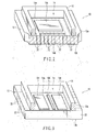
- a semiconductor package 10 according to a first embodiment of this invention will be described in detail with reference to FIGS. 1 to 3 .
- the semiconductor package 10 comprises a base plate 12 including a flat first surface 12a and a flat second surface 12b facing in a direction opposite to the first surface 12a.
- the base plate 12 is formed of a material which is high in thermal conductivity, for example, copper or copper alloy.
- a semiconductor element 14 is mounted at a predetermined region on the flat first surface 12a of the base plate 12.
- the semiconductor element 14 includes a semiconductor substrate 14a which is made of, for example, silicon and which is mounted at the predetermined region on the first surface 12a of the base plate 12, a heat generating unit 14b which generates a relatively large quantity of heat by operation like, for example, an integrated circuit and which is disposed or formed on the semiconductor substrate 14a, and various circuit units 14c which are disposed or formed around the heat generating unit 14b on the semiconductor substrate 14a.
- the various circuit units 14c include printed wirings (not shown) electrically connected to the heat generating unit 14b and generate only very small quantity of heat as compared with the heat generated by the heat generating unit 14b in operation.
- the various circuit units 14c include a plurality of external connection terminals 14d which project from the printed wirings and the first surface 12a of the base plate 12.
- the predetermined region on the first surface 12a of the base plate 12 is surrounded by a frame member 16, and an opening of the frame member 16 on the opposite side of the first surface 12a is closed by a lid 18.
- the plurality of external connection terminals 14d of the semiconductor element 14 penetrate through the frame member 16 and are exposed to an external space.
- An outer surface of the semiconductor package 10 is covered with a high-frequency current resistant material such as gold.
- a high-frequency current resistant material such as gold.
- Such covering is achieved by, for example, plating of the high-frequency current resistant material.
- the base plate 12 is detachably supported at a predetermined position on a supporting member 20 by means of a well known fixing element not shown, such as a plurality of fixing screws, while contacting the second surface 12b of the base plate 12 with the predetermined position on the supporting member 20.
- the supporting member 20 is also made of a metal material relatively high in thermal conductivity, but not so high as that of the base plate 12, such as aluminum or iron.
- the supporting member 20 may be a well known heat sink, and the well known heat sink may be an air-cooled structure or a liquid-cooled structure.
- a plurality of anisotropic heat conducting members 22 each having a sheet shape are disposed in the base plate 12 so that the anisotropic heat conducting members 22 intersect with the first surface 12a and the second surface 12b and are spaced from each other.
- Each anisotropic heat conducting member 22 orientates its higher thermal conductivity than the thermal conductivity of the base plate 12 in a direction from the first surface 12a toward the second surface 12b of the base plate 12.
- the majority of the plurality of anisotropic heat conducting members 22 intersects with the predetermined region enclosed by the frame member 16 on the first surface 12a of the base plate 12, that is, the region where the semiconductor substrate 14a of the semiconductor element 14 is mounted.
- each anisotropic heat conducting member 22 includes graphite sheet.
- At least a part of the plurality of anisotropic heat conducting members 22 intersects with the heat generating unit 14b of the semiconductor element 14 on the first surface 12a.
- the heat generating unit 14b of the semiconductor element 14 has a slender shape along the first surface 12a of the base plate 12. At least a part of the plurality of anisotropic heat conducting members 22 intersects with the heat generating unit 14c of the semiconductor element 14 on the first surface 12a in a direction orthogonal to the longitudinal direction of the heat generating unit 14c.
- the base plate 12 in which the plurality of anisotropic heat conducting members 22 are disposed in the predetermined layout as described above can be manufactured easily by a well known manufacturing method.
- the plurality of anisotropic heat conducting members 22 are disposed in the predetermined layout in a molding space (not shown) for the base plate 12 contained in a molding member (not shown)
- fine powder material for the base plate 12 is sequentially deposited in the molding space under a predetermined pressure.
- the heat generating unit 14b and various circuit units 14c of the semiconductor element 14 operate and generate heat.
- the majority of the heat is promptly transmitted from the predetermined region on which the heat generating unit 14b and various circuit units 14c of the semiconductor element 14 are mounted, on the first surface 12a of the base plate 12 to the second surface 12b by the plurality of anisotropic heat conducting members 22, and is diffused into the supporting member 20 through the second surface 12a of the base plate 12.
- the remaining heat is radiated into an external space through a region excluding the second surface 12b on the outer surface of the base plate 12.
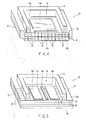
- FIG. 4 is a schematic sectional view of the semiconductor package 30 according to the second embodiment of the invention, which is like FIG. 2 ; and
- FIG. 5 is a schematic sectional view of the semiconductor package 30 according to the second embodiment of the invention, which is like FIG. 3 .
- the most structural members of the semiconductor package 30 are the same as those of the semiconductor package 10 according to the first embodiment of this invention and described above with reference to FIGS. 1 to 3 . Therefore, the structural members of the semiconductor package 30 which are the same as those of the semiconductor package 10 are denoted by the same reference numerals denoting the same structural members of the semiconductor package 10, and detailed explanation of them are omitted.
- the semiconductor package 30 of the second embodiment differs from the semiconductor package 10 of the first embodiment in that at least one thermal expansion control layer 32 is disposed along the first surface 12a between the first surface 12a and the second surface 12b in the base plate 12.
- the thermal expansion control layer 32 is formed of a material having a coefficient of thermal expansion substantially equivalent to that of the heat generating unit 14b of the semiconductor element 14.
- the thermal expansion control layer 32 securely prevents the semiconductor substrate 14a and the circuit units 14c including the printed wirings (not shown) and provided on the semiconductor substrate 14a from cracking while the coefficient of thermal expansion of the heat generating unit 14b is different from the coefficient of thermal expansion of the base plate 12 and the heat generating unit 14b generates heat of large quantity.
- the thermal expansion control layer 32 further prevents the base plate 12 from being distorted, so that a gap is not formed between the second surface 12b of the base plate 12 and the supporting member 20 (see FIG. 1 ) and a good heat transfer efficiency between the second surface 12b of the base plate 12 and the supporting member 20 (see FIG. 1 ) is maintained.
- thermal expansion control layer 32 is well known, and, for example, carbon cloth or molybdenum may be used.
- the thermal expansion control layer 32 can be disposed in the base plate 12 by the same manufacturing method as for the base plate 12 containing the plurality of anisotropic heat conducting members 22 in the semiconductor package 10 according to the first embodiment.
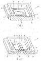
- FIG. 6 is a schematic sectional view of the semiconductor package 40 according to the third embodiment of the invention, which is like FIG. 2 ; and
- FIG. 7 is a schematic sectional view of the semiconductor package 40 according to the third embodiment of the invention, which is like FIG. 3 .
- the most structural members of the semiconductor package 40 are the same as those of the semiconductor package 10 according to the first embodiment of this invention and described above with reference to FIGS. 1 to 3 . Therefore, the structural members of the semiconductor package 40 which are the same as those of the semiconductor package 10 are denoted by the same reference numerals denoting the same structural members of the semiconductor package 10, and detailed explanation of them are omitted.
- the semiconductor package 40 of the third embodiment differs from the above described semiconductor package 10 of the first embodiment in the layout of a plurality of anisotropic heat conducting members 22' in the base plate 12.
- the plurality of anisotropic heat conducting members 22' of the semiconductor package 40 are similar to the plurality of anisotropic heat conducting members 22 of the semiconductor package 10 in the first embodiment. That is, the plurality of anisotropic heat conducting members 22' each having a sheet shape are disposed in the base plate 12 so that the anisotropic heat conducting members 22' intersect with the first surface 12a and the second surface 12b and are spaced from each other. Each anisotropic heat conducting member 22' orientates its higher thermal conductivity than the thermal conductivity of the base plate 12 in a direction from the first surface 12a toward the second surface 12b of the base plate 12.
- At least a part of the plurality of anisotropic heat conducting members 22' of the semiconductor package 40 intersects with the slender heat generating unit 14a of the semiconductor element 14 on the first surface 12a in a direction along the longitudinal direction of the heat generating unit 14a.
- the anisotropic heat conducting members 22' are spaced away from each other in parallel while extending from the heat generating unit 14b of the semiconductor element 14 on the first surface 12a toward the second surface 12b. This means that, in the semiconductor package 40 of this embodiment, when the base plate 12 is cut in a direction orthogonal to the longitudinal direction of the slender heat generating unit 14b as shown in FIG. 7 , the anisotropic heat conducting members 22' are arranged radially toward the second surface 12b from the heat generating unit 14b of the first surface 12b.
- heat generated from the heat generating unit 14b which generates the maximum quantity of heat in the semiconductor element 14 on the first surface 12a of the base plate 12 can be diffused efficiently to the second surface 12b. That is, the large quantity of heat generated in the heat generating unit 14b of the semiconductor element 14 on the first surface 12a of the base plate 12 can be efficiently transmitted to the supporting member 20 (see FIG. 1 ) through the second surface 12b of the base plate 12.
- the plurality of anisotropic heat conducting members 22' can be disposed in the base plate 12 by the same material and the same manufacturing method as those for the plurality of anisotropic heat conducting members 22 of the semiconductor package 10 in the first embodiment.
- At least one of a plurality of thermal expansion control layers 32 can be disposed in the base plate 12, so that the semiconductor package 40 of this embodiment can enjoy a desired function which can be obtained from the thermal expansion control layer 32.
- FIG. 8 is a schematic sectional view of the semiconductor package 50 according to the fourth embodiment of the invention, which is like FIG. 2 .
- the most structural members of the semiconductor package 50 are the same as those of the semiconductor package 10 according to the first embodiment of this invention and described above with reference to FIGS. 1 to 3 . Therefore, the structural members of the semiconductor package 50 which are the same as those of the semiconductor package 10 are denoted by the same reference numerals denoting the same structural members of the semiconductor package 10, and detailed explanation of them are omitted.
- the semiconductor package 50 of the fourth embodiment differs from the semiconductor package 10 of the first embodiment in the material of a plurality of anisotropic heat conducting members 52 in the base plate 12.
- Each anisotropic heat conducting member 52 includes a plurality of carbon nanotubes which are configured to a sheet shape.
- the plurality of anisotropic heat conducting members 52 of the semiconductor package 50 are similar to the plurality of anisotropic heat conducting members 22 of the semiconductor package 10 of the first embodiment. That is, the plurality of anisotropic heat conducting members 52 each having a sheet shape are disposed in the base plate 12 so that the anisotropic heat conducting members 52 intersect with the first surface 12a and the second surface 12b and are spaced from each other. Each anisotropic heat conducting member 52 orientates its higher thermal conductivity than the thermal conductivity of the base plate 12 in a direction from the first surface 12a toward the second surface 12b of the base plate 12.
- At least a part of the plurality of the anisotropic heat conducting members 52 intersects with the slender heat generating unit 14a of the semiconductor element 14 on the first surface 12a of the base plate 12 in a direction orthogonal to the longitudinal direction of the heat generating unit 14a.
- the plurality of anisotropic heat conducting members 52 can be disposed in the base plate 12 by the same manufacturing method as for the plurality of anisotropic heat conducting members 22 of the semiconductor package 10 in the first embodiment.
- the plurality of anisotropic heat conducting members 52 functions in the same way as the plurality of anisotropic heat conducting members 22 of the semiconductor package 10 in the first embodiment and can enjoy the same performance.
- FIG. 9 is a schematic sectional view of the semiconductor package 60 according to the fifth embodiment of the invention, which is like FIG. 3 .
- the most structural members of the semiconductor package 60 are the same as those of the semiconductor package 10 according to the first embodiment of this invention and described above with reference to FIGS. 1 to 3 . Therefore, the structural members of the semiconductor package 60 which are the same as those of the semiconductor package 10 are denoted by the same reference numerals denoting the same structural members of the semiconductor package 10, and detailed explanation of them are omitted.
- the semiconductor package 60 of the fifth embodiment differs from the semiconductor package 10 of the first embodiment in the material of a plurality of anisotropic heat conducting members 52' in the base plate 12.
- Each anisotropic heat conducting member 52' includes a plurality of carbon nanotubes which are configured to a sheet shape.
- the plurality of anisotropic heat conducting members 52' of the semiconductor package 60 are similar to the plurality of anisotropic heat conducting members 22 of the semiconductor package 10 of the first embodiment. That is, the plurality of anisotropic heat conducting members 52' each having a sheet shape are disposed in the base plate 12 so that the anisotropic heat conducting members 52' intersect with the first surface 12a and the second surface 12b and are spaced from each other. Each anisotropic heat conducting member 52' orientates its higher thermal conductivity than the thermal conductivity of the base plate 12 in a direction from the first surface 12a toward the second surface 12b of the base plate 12. But, like in the plurality of anisotropic heat conducting members 22' of the semiconductor package 40 of the third embodiment described above with reference to FIGS.
- the anisotropic heat conducting members 52' of the semiconductor package 60 intersects with the slender heat generating unit 14a of the semiconductor element 14 on the first surface 12a in a direction along the longitudinal direction of the heat generating unit 14a. Moreover, the anisotropic heat conducting members 52' are spaced away from each other in parallel while extending from the heat generating unit 14b of the semiconductor element 14 on the first surface 12a toward the second surface 12b. This means that, in the semiconductor package 60 of this embodiment, when the base plate 12 is cut in a direction orthogonal to the longitudinal direction of the slender heat generating unit 14b as shown in FIG. 9 , the anisotropic heat conducting members 52' are arranged radially toward the second surface 12b from the heat generating unit 14b of the first surface 12b.
- the plurality of anisotropic heat conducting members 52' can be disposed in the base plate 12 by the same manufacturing method as for the plurality of anisotropic heat conducting members 22 of the semiconductor package 10 in the first embodiment.
- the plurality of anisotropic heat conducting members 52' function in the same way as the plurality of anisotropic heat conducting members 22' of the semiconductor package 40 in the third embodiment shown in FIGS. 6 and 7 and can enjoy the same performance.
- FIG. 10 is a schematic sectional view of the semiconductor package 70 according to the sixth embodiment of the invention, which is like FIG. 2 .
- the semiconductor package 70 is configured by combining the structure of the semiconductor package 50 of the fourth embodiment described above with reference to FIG. 8 , with a plurality of thermal expansion control layers 32 used in the semiconductor package 30 according to the second embodiment described above with reference to FIGS. 4 and 5 .
- the semiconductor package 70 enjoys both the performance exhibited by the semiconductor package 50 of the fourth embodiment described above with reference to FIG. 8 and the performance exhibited by the plurality of thermal expansion control layers 32 used in the semiconductor package 30 of the second embodiment described above with reference to FIGS. 4 and 5 .
- FIG. 11 is a schematic sectional view of the semiconductor package 80 according to the seventh embodiment of this invention, which is like FIG. 3 .
- the semiconductor package 80 is configured by combining the semiconductor package 60 according to the fifth embodiment described above with reference to FIG. 9 , with a plurality of thermal expansion control layers 32 used in the semiconductor package 30 of the second embodiment described above with reference to FIGS. 4 and 5 .
- the semiconductor package 80 enjoys both the performance exhibited by the semiconductor package 60 of the fifth embodiment described above with reference to FIG. 9 and the performance exhibited by the plurality of thermal expansion control layers 32 used in the semiconductor package 30 of the second embodiment described above with reference to FIGS. 4 and 5 .
Landscapes
- Cooling Or The Like Of Semiconductors Or Solid State Devices (AREA)
Abstract
Description
- The present invention relates to a semiconductor package.
- A conventional semiconductor package comprises a base plate formed of a material high in thermal conductivity, for example, copper or copper alloy, and having a flat first surface and a flat second surface facing in the opposite direction to the first surface, and a semiconductor element mounted in a predetermined region on the flat first surface of the base plate. The second surface of the base plate is supported in a predetermined position on a supporting member. The supporting member is also made of a metal material relatively high in thermal conductivity, but not so high as that of the base plate, such as aluminum or iron.
- The semiconductor element includes a semiconductor substrate made of, for example, silicon and mounted in the predetermined region on the first surface of the base plate, a heat generating unit disposed or formed on the semiconductor substrate and generating a relatively large quantity of heat by operation like, for example, an integrated circuit, and various circuit units disposed or formed around the heat generating unit on the semiconductor substrate. The various circuit units include printed wirings electrically connected to the heat generating unit and generate only very small quantity of heat as compared with the heat generated by the heat generating unit in operation. The various circuit units include a plurality of external connection terminals projecting from the printed wirings and the first surface of the base plate.
- The predetermined region on the first surface of the base plate is surrounded by a frame member, and an opening of the frame member on the opposite side of the first surface is closed by a lid. The plurality of external connection terminals of the semiconductor element penetrate through the frame member and are exposed to an external space.
- When electric signals are input to the plurality of external connection terminals of the semiconductor element, the heat generating unit and various circuit units of the semiconductor element operate and generate heat. The heat is radiated to an external space through a region excluding the second surface on the outer surface of the base plate or is diffused to the supporting member through the second surface of the base plate.
- Along with the recent trend in which the performance of the semiconductor element becomes higher, the quantity of heat generated in the heat generating unit is increasing steeply. The semiconductor element cannot exhibit its predetermined performance when its temperature exceeds a predetermined value. Recently, therefore, the base plate is provided with various cooling measures in order to enhance the heat radiation effect from the base plate.
- These conventional various cooling measures includes, for example, a direct attachment of a heat sink having a plurality of cooling fins to the second surface of the base plate or a combination of a high heat conductive element of a material having a higher thermal conductivity than that of the base plate, such as a graphite sheet, and adhered to the second surface and the heat sink additionally mounted on the high heat conductive element. The graphite sheet combined with the heat sink and adhered to the second surface is disclosed in, for example, Japanese Patent Application KOKAI Publication No.
2004-288949 - In such conventional cooling measures, the heat generated by the heat generating unit of the semiconductor element on the first surface is transferred to the second surface in the base plate, and is positively discharged from the second surface by means of the heat sink.
- Considering, however, the present development scene of semiconductor elements, that is, the degree of increasing of heat density caused by progress of performance and reduction of outer size, it is desired to develop cooling measures having higher cooling performance than that of the conventional cooling measures for ensuring the predetermined high performance of recent advanced semiconductor elements.
- This invention is derived from these circumstances, and an object of of this invention is to provide a semiconductor package having cooling measures higher in cooling performance than the conventional cooling measures.
- According to one aspect of this invention, a semiconductor package comprises a base plate having first and second surfaces both facing in opposite directions and a heat conducting element disposed in the base plate and intersecting with the first and second surfaces. A semiconductor element having a heat generating unit is mounted on the first surface, and the second surface is supported on a supporting member having a thermal conductivity. The heat conducting element orientates a direction of higher thermal conductivity than the thermal conductivity of the base plate in a direction from the first surface toward the second surface. The semiconductor package is characterized in that the heat generating unit comprises a plurality of anisotropic heat conducting members disposed in the base plate and spaced away from each other. Each anisotropic heat conducting member has a sheet shape intersecting with the first surface and the second surface and orientates a direction of higher thermal conductivity than the thermal conductivity of the base plate in a direction from the first surface toward the second surface.
- The invention can be more fully understood from the following detailed description when taken in conjunction with accompanying drawings, in which:
-
FIG. 1 is a perspective exploded view schematically showing a semiconductor package according to a first embodiment of this invention; -
FIG. 2 is a schematic sectional view along a line II-II ofFIG. 1 ; -
FIG. 3 is a schematic sectional view along a line III-III ofFIG. 1 ; -
FIG. 4 is a schematic sectional view of a semiconductor package according to a second embodiment of this invention, which is likeFIG. 2 ; -
FIG. 5 is a schematic sectional view of the semiconductor package according to the second embodiment of this invention, which is likeFIG. 3 ; -
FIG. 6 is a schematic sectional view of a semiconductor package according to a third embodiment of this invention, which is likeFIG. 2 ; -
FIG. 7 is a schematic sectional view of the semiconductor package according to the third embodiment of this invention, which is likeFIG. 3 ; -
FIG. 8 is a schematic sectional view of a semiconductor package according to a fourth embodiment of this invention, which is likeFIG. 2 ; -
FIG. 9 is a schematic sectional view of a semiconductor package according to a fifth embodiment of this invention, which is likeFIG. 3 ; -
FIG. 10 is a schematic sectional view of a semiconductor package according to a sixth embodiment of this invention, which is likeFIG. 2 ; and -
FIG. 11 is a schematic sectional view of a semiconductor package according to a seventh embodiment of this invention, which is likeFIG. 3 . - A
semiconductor package 10 according to a first embodiment of this invention will be described in detail with reference toFIGS. 1 to 3 . - As shown in
FIG. 1 , thesemiconductor package 10 comprises abase plate 12 including a flatfirst surface 12a and aflat second surface 12b facing in a direction opposite to thefirst surface 12a. Thebase plate 12 is formed of a material which is high in thermal conductivity, for example, copper or copper alloy. - A
semiconductor element 14 is mounted at a predetermined region on the flatfirst surface 12a of thebase plate 12. Thesemiconductor element 14 includes asemiconductor substrate 14a which is made of, for example, silicon and which is mounted at the predetermined region on thefirst surface 12a of thebase plate 12, aheat generating unit 14b which generates a relatively large quantity of heat by operation like, for example, an integrated circuit and which is disposed or formed on thesemiconductor substrate 14a, andvarious circuit units 14c which are disposed or formed around theheat generating unit 14b on thesemiconductor substrate 14a. Thevarious circuit units 14c include printed wirings (not shown) electrically connected to theheat generating unit 14b and generate only very small quantity of heat as compared with the heat generated by theheat generating unit 14b in operation. Thevarious circuit units 14c include a plurality ofexternal connection terminals 14d which project from the printed wirings and thefirst surface 12a of thebase plate 12. - The predetermined region on the
first surface 12a of thebase plate 12 is surrounded by aframe member 16, and an opening of theframe member 16 on the opposite side of thefirst surface 12a is closed by alid 18. The plurality ofexternal connection terminals 14d of thesemiconductor element 14 penetrate through theframe member 16 and are exposed to an external space. - An outer surface of the
semiconductor package 10 is covered with a high-frequency current resistant material such as gold. Such covering is achieved by, for example, plating of the high-frequency current resistant material. - The
base plate 12 is detachably supported at a predetermined position on a supportingmember 20 by means of a well known fixing element not shown, such as a plurality of fixing screws, while contacting thesecond surface 12b of thebase plate 12 with the predetermined position on the supportingmember 20. The supportingmember 20 is also made of a metal material relatively high in thermal conductivity, but not so high as that of thebase plate 12, such as aluminum or iron. - The supporting
member 20 may be a well known heat sink, and the well known heat sink may be an air-cooled structure or a liquid-cooled structure. - As shown in
FIGS. 2 and 3 , a plurality of anisotropicheat conducting members 22 each having a sheet shape are disposed in thebase plate 12 so that the anisotropicheat conducting members 22 intersect with thefirst surface 12a and thesecond surface 12b and are spaced from each other. Each anisotropicheat conducting member 22 orientates its higher thermal conductivity than the thermal conductivity of thebase plate 12 in a direction from thefirst surface 12a toward thesecond surface 12b of thebase plate 12. - The majority of the plurality of anisotropic
heat conducting members 22 intersects with the predetermined region enclosed by theframe member 16 on thefirst surface 12a of thebase plate 12, that is, the region where thesemiconductor substrate 14a of thesemiconductor element 14 is mounted. - In this embodiment, each anisotropic
heat conducting member 22 includes graphite sheet. - At least a part of the plurality of anisotropic
heat conducting members 22 intersects with theheat generating unit 14b of thesemiconductor element 14 on thefirst surface 12a. - In this embodiment, the
heat generating unit 14b of thesemiconductor element 14 has a slender shape along thefirst surface 12a of thebase plate 12. At least a part of the plurality of anisotropicheat conducting members 22 intersects with theheat generating unit 14c of thesemiconductor element 14 on thefirst surface 12a in a direction orthogonal to the longitudinal direction of theheat generating unit 14c. - The
base plate 12 in which the plurality of anisotropicheat conducting members 22 are disposed in the predetermined layout as described above can be manufactured easily by a well known manufacturing method. For example, while the plurality of anisotropicheat conducting members 22 are disposed in the predetermined layout in a molding space (not shown) for thebase plate 12 contained in a molding member (not shown), fine powder material for thebase plate 12 is sequentially deposited in the molding space under a predetermined pressure. - In the
semiconductor package 10 according to the first embodiment of this invention and configured as described above in detail, when predetermined electric signals are input to the plurality ofexternal connection terminals 14b of thesemiconductor element 14, theheat generating unit 14b andvarious circuit units 14c of thesemiconductor element 14 operate and generate heat. The majority of the heat is promptly transmitted from the predetermined region on which theheat generating unit 14b andvarious circuit units 14c of thesemiconductor element 14 are mounted, on thefirst surface 12a of thebase plate 12 to thesecond surface 12b by the plurality of anisotropicheat conducting members 22, and is diffused into the supportingmember 20 through thesecond surface 12a of thebase plate 12. - The remaining heat is radiated into an external space through a region excluding the
second surface 12b on the outer surface of thebase plate 12. - Next, a
semiconductor package 30 according to a second embodiment of this invention will be described in detail with reference toFIGS. 4 and 5. FIG. 4 is a schematic sectional view of thesemiconductor package 30 according to the second embodiment of the invention, which is likeFIG. 2 ; andFIG. 5 is a schematic sectional view of thesemiconductor package 30 according to the second embodiment of the invention, which is likeFIG. 3 . - The most structural members of the
semiconductor package 30 are the same as those of thesemiconductor package 10 according to the first embodiment of this invention and described above with reference toFIGS. 1 to 3 . Therefore, the structural members of thesemiconductor package 30 which are the same as those of thesemiconductor package 10 are denoted by the same reference numerals denoting the same structural members of thesemiconductor package 10, and detailed explanation of them are omitted. - The
semiconductor package 30 of the second embodiment differs from thesemiconductor package 10 of the first embodiment in that at least one thermalexpansion control layer 32 is disposed along thefirst surface 12a between thefirst surface 12a and thesecond surface 12b in thebase plate 12. The thermalexpansion control layer 32 is formed of a material having a coefficient of thermal expansion substantially equivalent to that of theheat generating unit 14b of thesemiconductor element 14. The thermalexpansion control layer 32 securely prevents thesemiconductor substrate 14a and thecircuit units 14c including the printed wirings (not shown) and provided on thesemiconductor substrate 14a from cracking while the coefficient of thermal expansion of theheat generating unit 14b is different from the coefficient of thermal expansion of thebase plate 12 and theheat generating unit 14b generates heat of large quantity. The thermalexpansion control layer 32 further prevents thebase plate 12 from being distorted, so that a gap is not formed between thesecond surface 12b of thebase plate 12 and the supporting member 20 (seeFIG. 1 ) and a good heat transfer efficiency between thesecond surface 12b of thebase plate 12 and the supporting member 20 (seeFIG. 1 ) is maintained. - The material for such thermal
expansion control layer 32 is well known, and, for example, carbon cloth or molybdenum may be used. The thermalexpansion control layer 32 can be disposed in thebase plate 12 by the same manufacturing method as for thebase plate 12 containing the plurality of anisotropicheat conducting members 22 in thesemiconductor package 10 according to the first embodiment. - Next, a
semiconductor package 40 according to a third embodiment of this invention will be described in detail with reference toFIGS. 6 and 7. FIG. 6 is a schematic sectional view of thesemiconductor package 40 according to the third embodiment of the invention, which is likeFIG. 2 ; andFIG. 7 is a schematic sectional view of thesemiconductor package 40 according to the third embodiment of the invention, which is likeFIG. 3 . - The most structural members of the
semiconductor package 40 are the same as those of thesemiconductor package 10 according to the first embodiment of this invention and described above with reference toFIGS. 1 to 3 . Therefore, the structural members of thesemiconductor package 40 which are the same as those of thesemiconductor package 10 are denoted by the same reference numerals denoting the same structural members of thesemiconductor package 10, and detailed explanation of them are omitted. - The
semiconductor package 40 of the third embodiment differs from the above describedsemiconductor package 10 of the first embodiment in the layout of a plurality of anisotropic heat conducting members 22' in thebase plate 12. - The plurality of anisotropic heat conducting members 22' of the
semiconductor package 40 are similar to the plurality of anisotropicheat conducting members 22 of thesemiconductor package 10 in the first embodiment. That is, the plurality of anisotropic heat conducting members 22' each having a sheet shape are disposed in thebase plate 12 so that the anisotropic heat conducting members 22' intersect with thefirst surface 12a and thesecond surface 12b and are spaced from each other. Each anisotropic heat conducting member 22' orientates its higher thermal conductivity than the thermal conductivity of thebase plate 12 in a direction from thefirst surface 12a toward thesecond surface 12b of thebase plate 12. - However, at least a part of the plurality of anisotropic heat conducting members 22' of the
semiconductor package 40 intersects with the slenderheat generating unit 14a of thesemiconductor element 14 on thefirst surface 12a in a direction along the longitudinal direction of theheat generating unit 14a. - Moreover, the anisotropic heat conducting members 22' are spaced away from each other in parallel while extending from the
heat generating unit 14b of thesemiconductor element 14 on thefirst surface 12a toward thesecond surface 12b. This means that, in thesemiconductor package 40 of this embodiment, when thebase plate 12 is cut in a direction orthogonal to the longitudinal direction of the slenderheat generating unit 14b as shown inFIG. 7 , the anisotropic heat conducting members 22' are arranged radially toward thesecond surface 12b from theheat generating unit 14b of thefirst surface 12b. - In such configuration, heat generated from the
heat generating unit 14b which generates the maximum quantity of heat in thesemiconductor element 14 on thefirst surface 12a of thebase plate 12 can be diffused efficiently to thesecond surface 12b. That is, the large quantity of heat generated in theheat generating unit 14b of thesemiconductor element 14 on thefirst surface 12a of thebase plate 12 can be efficiently transmitted to the supporting member 20 (seeFIG. 1 ) through thesecond surface 12b of thebase plate 12. - The plurality of anisotropic heat conducting members 22' can be disposed in the
base plate 12 by the same material and the same manufacturing method as those for the plurality of anisotropicheat conducting members 22 of thesemiconductor package 10 in the first embodiment. - Also in this embodiment, as in the
semiconductor package 30 of the second embodiment described above with reference toFIGS. 4 and 5 , at least one of a plurality of thermal expansion control layers 32 can be disposed in thebase plate 12, so that thesemiconductor package 40 of this embodiment can enjoy a desired function which can be obtained from the thermalexpansion control layer 32. - Next, a
semiconductor package 50 according to a fourth embodiment of this invention will be described in detail with reference toFIG. 8. FIG. 8 is a schematic sectional view of thesemiconductor package 50 according to the fourth embodiment of the invention, which is likeFIG. 2 . - The most structural members of the
semiconductor package 50 are the same as those of thesemiconductor package 10 according to the first embodiment of this invention and described above with reference toFIGS. 1 to 3 . Therefore, the structural members of thesemiconductor package 50 which are the same as those of thesemiconductor package 10 are denoted by the same reference numerals denoting the same structural members of thesemiconductor package 10, and detailed explanation of them are omitted. - The
semiconductor package 50 of the fourth embodiment differs from thesemiconductor package 10 of the first embodiment in the material of a plurality of anisotropicheat conducting members 52 in thebase plate 12. Each anisotropicheat conducting member 52 includes a plurality of carbon nanotubes which are configured to a sheet shape. - The plurality of anisotropic
heat conducting members 52 of thesemiconductor package 50 are similar to the plurality of anisotropicheat conducting members 22 of thesemiconductor package 10 of the first embodiment. That is, the plurality of anisotropicheat conducting members 52 each having a sheet shape are disposed in thebase plate 12 so that the anisotropicheat conducting members 52 intersect with thefirst surface 12a and thesecond surface 12b and are spaced from each other. Each anisotropicheat conducting member 52 orientates its higher thermal conductivity than the thermal conductivity of thebase plate 12 in a direction from thefirst surface 12a toward thesecond surface 12b of thebase plate 12. Moreover, like in the plurality of anisotropicheat conducting members 22 of thesemiconductor package 10 of the first embodiment, at least a part of the plurality of the anisotropicheat conducting members 52 intersects with the slenderheat generating unit 14a of thesemiconductor element 14 on thefirst surface 12a of thebase plate 12 in a direction orthogonal to the longitudinal direction of theheat generating unit 14a. - The plurality of anisotropic
heat conducting members 52 can be disposed in thebase plate 12 by the same manufacturing method as for the plurality of anisotropicheat conducting members 22 of thesemiconductor package 10 in the first embodiment. The plurality of anisotropicheat conducting members 52 functions in the same way as the plurality of anisotropicheat conducting members 22 of thesemiconductor package 10 in the first embodiment and can enjoy the same performance. - Next, a
semiconductor package 60 according to a fifth embodiment of this invention will be described in detail with reference toFIG. 9. FIG. 9 is a schematic sectional view of thesemiconductor package 60 according to the fifth embodiment of the invention, which is likeFIG. 3 . - The most structural members of the
semiconductor package 60 are the same as those of thesemiconductor package 10 according to the first embodiment of this invention and described above with reference toFIGS. 1 to 3 . Therefore, the structural members of thesemiconductor package 60 which are the same as those of thesemiconductor package 10 are denoted by the same reference numerals denoting the same structural members of thesemiconductor package 10, and detailed explanation of them are omitted. - The
semiconductor package 60 of the fifth embodiment differs from thesemiconductor package 10 of the first embodiment in the material of a plurality of anisotropic heat conducting members 52' in thebase plate 12. Each anisotropic heat conducting member 52' includes a plurality of carbon nanotubes which are configured to a sheet shape. - The plurality of anisotropic heat conducting members 52' of the
semiconductor package 60 are similar to the plurality of anisotropicheat conducting members 22 of thesemiconductor package 10 of the first embodiment. That is, the plurality of anisotropic heat conducting members 52' each having a sheet shape are disposed in thebase plate 12 so that the anisotropic heat conducting members 52' intersect with thefirst surface 12a and thesecond surface 12b and are spaced from each other. Each anisotropic heat conducting member 52' orientates its higher thermal conductivity than the thermal conductivity of thebase plate 12 in a direction from thefirst surface 12a toward thesecond surface 12b of thebase plate 12. But, like in the plurality of anisotropic heat conducting members 22' of thesemiconductor package 40 of the third embodiment described above with reference toFIGS. 6 and 7 , at least a part of the plurality of anisotropic heat conducting members 52' of thesemiconductor package 60 intersects with the slenderheat generating unit 14a of thesemiconductor element 14 on thefirst surface 12a in a direction along the longitudinal direction of theheat generating unit 14a. Moreover, the anisotropic heat conducting members 52' are spaced away from each other in parallel while extending from theheat generating unit 14b of thesemiconductor element 14 on thefirst surface 12a toward thesecond surface 12b. This means that, in thesemiconductor package 60 of this embodiment, when thebase plate 12 is cut in a direction orthogonal to the longitudinal direction of the slenderheat generating unit 14b as shown inFIG. 9 , the anisotropic heat conducting members 52' are arranged radially toward thesecond surface 12b from theheat generating unit 14b of thefirst surface 12b. - The plurality of anisotropic heat conducting members 52' can be disposed in the
base plate 12 by the same manufacturing method as for the plurality of anisotropicheat conducting members 22 of thesemiconductor package 10 in the first embodiment. The plurality of anisotropic heat conducting members 52' function in the same way as the plurality of anisotropic heat conducting members 22' of thesemiconductor package 40 in the third embodiment shown inFIGS. 6 and 7 and can enjoy the same performance. - Next, a
semiconductor package 70 according to a sixth embodiment of this invention will be described in detail with reference toFIG. 10. FIG. 10 is a schematic sectional view of thesemiconductor package 70 according to the sixth embodiment of the invention, which is likeFIG. 2 . - The
semiconductor package 70 is configured by combining the structure of thesemiconductor package 50 of the fourth embodiment described above with reference toFIG. 8 , with a plurality of thermal expansion control layers 32 used in thesemiconductor package 30 according to the second embodiment described above with reference toFIGS. 4 and 5 . - Therefore, the
semiconductor package 70 enjoys both the performance exhibited by thesemiconductor package 50 of the fourth embodiment described above with reference toFIG. 8 and the performance exhibited by the plurality of thermal expansion control layers 32 used in thesemiconductor package 30 of the second embodiment described above with reference toFIGS. 4 and 5 . - Next, a
semiconductor package 80 according to a seventh embodiment of this invention will be described in detail with reference toFIG. 11. FIG. 11 is a schematic sectional view of thesemiconductor package 80 according to the seventh embodiment of this invention, which is likeFIG. 3 . - The
semiconductor package 80 is configured by combining thesemiconductor package 60 according to the fifth embodiment described above with reference toFIG. 9 , with a plurality of thermal expansion control layers 32 used in thesemiconductor package 30 of the second embodiment described above with reference toFIGS. 4 and 5 . - Therefore, the
semiconductor package 80 enjoys both the performance exhibited by thesemiconductor package 60 of the fifth embodiment described above with reference toFIG. 9 and the performance exhibited by the plurality of thermal expansion control layers 32 used in thesemiconductor package 30 of the second embodiment described above with reference toFIGS. 4 and 5 .
Claims (8)
- A semiconductor package (10, 30, 40, 50, 60, 70, 80) comprising: a base plate (12) including a first surface (12a) on which a semiconductor element (14) having a heat generating unit (14a) is mounted, and a second surface (12b) facing in the opposite direction to the first surface and supported on a supporting member (20) having a thermal conductivity; and a heat conducting element disposed in the base plate, intersecting with the first surface and the second surface and orientating a direction of higher thermal conductivity than the thermal conductivity of the base plate in a direction from the first surface toward the second surface, the semiconductor package characterized in that
the heat conducting element comprises a plurality of anisotropic heat conducting members (22, 22', 52, 52') disposed in the base plate (12) and spaced away from each other, each having a sheet shape intersecting with the first surface (12a) and the second surface (12b), and each orientating a direction of higher thermal conductivity than the thermal conductivity of the base plate in a direction from the first surface toward the second surface. - The semiconductor package (10, 30, 40, 50, 60, 70, 80) according to claim 1, characterized in that at least a part of the plurality of anisotropic heat conducting members (22, 22', 52, 52') intersects with the heat generating unit (14a) of the semiconductor element (14) on the first surface (12a).
- The semiconductor package (10, 30, 50, 70) according to claim 2, characterized in that
the heat generating unit (14a) of the semiconductor element (14) has a slender shape along the first surface (12a) of the base plate (12), and
at least a part of the plurality of anisotropic heat conducting members (22, 52) intersects with the heat generating unit (14a) of the semiconductor element (14) on the first surface (12a) in a direction orthogonal to a longitudinal direction of the heat generating unit (14a). - The semiconductor package (40, 60, 80) according to claim 2, characterized in that
the heat generating unit (14a) of the semiconductor element (14) has a slender shape along the first surface (12a) of the base plate (12), and
at least a part of the plurality of anisotropic heat conducting members (22', 52') intersects with the heat generating unit (14a) of the semiconductor element (14) on the first surface (12a) in a direction along a longitudinal direction of the heat generating unit (14a). - The semiconductor package (40, 60, 80) according to claim 4, characterized in that the anisotropic heat conducting members (22', 52') are spaced away from each other in parallel while extending from the heat generating unit (14a) of the semiconductor element (14) on the first surface (12a) to the second surface (12b).
- The semiconductor package (30, 70, 80) according to any one of claims 1 to 5, characterized by further comprising a thermal expansion control layer (32) having substantially the same coefficient of thermal expansion as that of the heat generating unit (14a) of the semiconductor element (14) and disposed along the first surface (12a) between the first surface (12a) and the second surface (12b) in the base plate (12).
- The semiconductor package (10, 30, 40) according to any one of claims 1 to 6, characterized in that each of the plurality of anisotropic heat conducting members (22, 22') includes a graphite sheet.
- The semiconductor package (50, 60, 70, 80) according to any one of claims 1 to 6, characterized in that each of the plurality of anisotropic heat conducting members (52, 52') includes a plurality of carbon nanotubes.
Applications Claiming Priority (1)
| Application Number | Priority Date | Filing Date | Title |
|---|---|---|---|
| JP2007205846A JP4504401B2 (en) | 2007-08-07 | 2007-08-07 | Semiconductor package |
Publications (3)
| Publication Number | Publication Date |
|---|---|
| EP2023388A2 true EP2023388A2 (en) | 2009-02-11 |
| EP2023388A3 EP2023388A3 (en) | 2009-11-11 |
| EP2023388B1 EP2023388B1 (en) | 2011-02-09 |
Family
ID=39765042
Family Applications (1)
| Application Number | Title | Priority Date | Filing Date |
|---|---|---|---|
| EP08252629A Not-in-force EP2023388B1 (en) | 2007-08-07 | 2008-08-05 | Semiconductor package |
Country Status (4)
| Country | Link |
|---|---|
| US (1) | US7868450B2 (en) |
| EP (1) | EP2023388B1 (en) |
| JP (1) | JP4504401B2 (en) |
| DE (1) | DE602008004858D1 (en) |
Families Citing this family (13)
| Publication number | Priority date | Publication date | Assignee | Title |
|---|---|---|---|---|
| JP5112101B2 (en) * | 2007-02-15 | 2013-01-09 | 株式会社東芝 | Semiconductor package |
| JP5013116B2 (en) * | 2007-12-11 | 2012-08-29 | 富士通株式会社 | Sheet-like structure, method for producing the same, and electronic device |
| US20100091477A1 (en) * | 2008-10-14 | 2010-04-15 | Kabushiki Kaisha Toshiba | Package, and fabrication method for the package |
| JP4643703B2 (en) * | 2008-11-21 | 2011-03-02 | 株式会社東芝 | Semiconductor device fixture and mounting structure thereof |
| US8477499B2 (en) | 2009-06-05 | 2013-07-02 | Laird Technologies, Inc. | Assemblies and methods for dissipating heat from handheld electronic devices |
| WO2011010394A1 (en) | 2009-07-21 | 2011-01-27 | トヨタ自動車株式会社 | Seed-crystal shaft for single-crystal growth by solution method |
| JP5806464B2 (en) * | 2010-02-03 | 2015-11-10 | 株式会社東芝 | Semiconductor element storage package and semiconductor device using the same |
| JP2011258755A (en) * | 2010-06-09 | 2011-12-22 | Denso Corp | Heat spreader and cooling device for heating element |
| JP5397340B2 (en) * | 2010-07-22 | 2014-01-22 | 株式会社デンソー | Semiconductor cooling device |
| JP5450313B2 (en) | 2010-08-06 | 2014-03-26 | 株式会社東芝 | High frequency semiconductor package and manufacturing method thereof |
| JP5621698B2 (en) * | 2011-04-08 | 2014-11-12 | 株式会社日本自動車部品総合研究所 | Heating element module and manufacturing method thereof |
| EP3780080A4 (en) * | 2018-03-28 | 2021-12-29 | Kyocera Corporation | Electronic element mounting substrate, electronic device, and electronic module |
| WO2020004459A1 (en) * | 2018-06-26 | 2020-01-02 | 京セラ株式会社 | Electronic element mounting substrate, electronic device, and electronic module |
Citations (1)
| Publication number | Priority date | Publication date | Assignee | Title |
|---|---|---|---|---|
| JP2004288949A (en) | 2002-11-26 | 2004-10-14 | Kyocera Corp | Semiconductor element storage package and semiconductor device |
Family Cites Families (26)
| Publication number | Priority date | Publication date | Assignee | Title |
|---|---|---|---|---|
| JPH09129793A (en) | 1995-10-27 | 1997-05-16 | Tonen Corp | Heat transfer plate for semiconductor package |
| JP2000273196A (en) | 1999-03-24 | 2000-10-03 | Polymatech Co Ltd | Thermal conductive resin substrate and semiconductor package |
| JP2001118974A (en) * | 1999-10-15 | 2001-04-27 | Mitsubishi Chemicals Corp | Heat sink |
| JP2001313345A (en) | 2000-04-28 | 2001-11-09 | Kyocera Corp | Package for storing semiconductor elements |
| US7332819B2 (en) * | 2002-01-09 | 2008-02-19 | Micron Technology, Inc. | Stacked die in die BGA package |
| AT413163B (en) * | 2001-12-18 | 2005-11-15 | Fotec Forschungs Und Technolog | COOLING DEVICE FOR A CHIP AND METHOD OF MANUFACTURE |
| JP2004076044A (en) * | 2002-08-12 | 2004-03-11 | Sumitomo Electric Ind Ltd | Ceramic-metal composite material and method for producing the same |
| ATE474443T1 (en) * | 2003-02-07 | 2010-07-15 | Panasonic Corp | LIGHTING DEVICE USING A BASE TO MOUNT A FLAT LED MODULE ON A HEATSINK |
| JP2005255503A (en) * | 2004-03-15 | 2005-09-22 | Matsushita Electric Ind Co Ltd | Low thermal expansion composite |
| JP2005272164A (en) * | 2004-03-23 | 2005-10-06 | Matsushita Electric Ind Co Ltd | High thermal conductivity member, method for manufacturing the same, and heat dissipation system using the same |
| JP2006045596A (en) * | 2004-08-02 | 2006-02-16 | Hitachi Metals Ltd | Composite body with high thermal conductivity and low thermal expansion, and its manufacturing method |
| JP2006093526A (en) * | 2004-09-27 | 2006-04-06 | Matsushita Electric Ind Co Ltd | Conductive heat conductive sheet |
| JP2006114826A (en) * | 2004-10-18 | 2006-04-27 | Yamaha Corp | Thermally conductive substrate, thermoelectric module, and method for producing thermally conductive substrate |
| US7361985B2 (en) * | 2004-10-27 | 2008-04-22 | Freescale Semiconductor, Inc. | Thermally enhanced molded package for semiconductors |
| JP2006144030A (en) * | 2004-11-16 | 2006-06-08 | Bridgestone Corp | High thermal conductive composite material and its manufacturing method |
| WO2006086738A1 (en) * | 2005-02-11 | 2006-08-17 | Heat Technnology, Inc. | Heat sink having directive heat elements |
| US20080118742A1 (en) * | 2005-02-16 | 2008-05-22 | Hitachi Metals, Ltd. | Heat Spreading Member And Manufacturing Method Thereof |
| JP2006261255A (en) * | 2005-03-16 | 2006-09-28 | Matsushita Electric Ind Co Ltd | Semiconductor device |
| JP2006310806A (en) * | 2005-03-28 | 2006-11-09 | Kyocera Corp | Heat dissipation member, electronic component mounting board, electronic component storage package, and electronic device |
| CN100404242C (en) * | 2005-04-14 | 2008-07-23 | 清华大学 | Thermal interface material and method of manufacturing the same |
| JP4608641B2 (en) * | 2005-04-27 | 2011-01-12 | 株式会社豊田自動織機 | Power module heat sink |
| JP5098642B2 (en) * | 2005-06-16 | 2012-12-12 | パナソニック株式会社 | Method for producing heat-dissipating graphite sheet |
| JP4686274B2 (en) * | 2005-06-30 | 2011-05-25 | ポリマテック株式会社 | Heat dissipation component and manufacturing method thereof |
| JP2007059875A (en) * | 2005-07-26 | 2007-03-08 | Kyocera Corp | Heat dissipation member, electronic component storage package and electronic device using the same |
| US7359205B1 (en) * | 2005-11-09 | 2008-04-15 | Nvidia Corporation | Bottom exit of exhaust air from a chassis to reduce acoustics emission |
| US7760507B2 (en) * | 2007-12-26 | 2010-07-20 | The Bergquist Company | Thermally and electrically conductive interconnect structures |
-
2007
- 2007-08-07 JP JP2007205846A patent/JP4504401B2/en not_active Expired - Fee Related
-
2008
- 2008-08-05 US US12/186,129 patent/US7868450B2/en not_active Expired - Fee Related
- 2008-08-05 DE DE602008004858T patent/DE602008004858D1/en active Active
- 2008-08-05 EP EP08252629A patent/EP2023388B1/en not_active Not-in-force
Patent Citations (1)
| Publication number | Priority date | Publication date | Assignee | Title |
|---|---|---|---|---|
| JP2004288949A (en) | 2002-11-26 | 2004-10-14 | Kyocera Corp | Semiconductor element storage package and semiconductor device |
Also Published As
| Publication number | Publication date |
|---|---|
| JP2009043851A (en) | 2009-02-26 |
| EP2023388A3 (en) | 2009-11-11 |
| EP2023388B1 (en) | 2011-02-09 |
| JP4504401B2 (en) | 2010-07-14 |
| US20090039500A1 (en) | 2009-02-12 |
| US7868450B2 (en) | 2011-01-11 |
| DE602008004858D1 (en) | 2011-03-24 |
Similar Documents
| Publication | Publication Date | Title |
|---|---|---|
| EP2023388B1 (en) | Semiconductor package | |
| US20110235278A1 (en) | Circuit module | |
| US9997432B2 (en) | Semiconductor device and electronic component using the same | |
| KR100253056B1 (en) | Cooling structure of the member | |
| CN107708286B (en) | Printed circuit board assembly | |
| EP3695438B1 (en) | Heat sink, integrated circuit chip and circuit board | |
| EP1058491A3 (en) | Printed wiring board structure with integral metal matrix composite core | |
| US6778398B2 (en) | Thermal-conductive substrate package | |
| JPH10247703A (en) | Ball grid array package and printed board | |
| KR101260179B1 (en) | A Laminated Heat Dissipating Plate and An Electronic Assembly Structure Using the Same | |
| JP2006093526A (en) | Conductive heat conductive sheet | |
| JP6098705B1 (en) | Inverter | |
| CN113268127A (en) | Electronic device | |
| JP6686467B2 (en) | Electronic component heat dissipation structure | |
| JP5100165B2 (en) | Cooling board | |
| JPH1168263A (en) | Electronic circuit board | |
| JP2003152368A (en) | Electronics | |
| US20060220188A1 (en) | Package structure having mixed circuit and composite substrate | |
| JP2003318579A (en) | Heat dissipation method of FET with heat sink | |
| US6399877B1 (en) | Heat sink | |
| JP2005158914A (en) | Printed circuit board | |
| CN223584567U (en) | A heat dissipation system | |
| JP2024000197A (en) | Semiconductor devices and semiconductor device manufacturing methods | |
| EP1950805A1 (en) | Electronic element, package having same, and electronic device | |
| JP5088939B2 (en) | Laminated board |
Legal Events
| Date | Code | Title | Description |
|---|---|---|---|
| PUAI | Public reference made under article 153(3) epc to a published international application that has entered the european phase |
Free format text: ORIGINAL CODE: 0009012 |
|
| 17P | Request for examination filed |
Effective date: 20080811 |
|
| AK | Designated contracting states |
Kind code of ref document: A2 Designated state(s): AT BE BG CH CY CZ DE DK EE ES FI FR GB GR HR HU IE IS IT LI LT LU LV MC MT NL NO PL PT RO SE SI SK TR |
|
| AX | Request for extension of the european patent |
Extension state: AL BA MK RS |
|
| PUAL | Search report despatched |
Free format text: ORIGINAL CODE: 0009013 |
|
| AK | Designated contracting states |
Kind code of ref document: A3 Designated state(s): AT BE BG CH CY CZ DE DK EE ES FI FR GB GR HR HU IE IS IT LI LT LU LV MC MT NL NO PL PT RO SE SI SK TR |
|
| AX | Request for extension of the european patent |
Extension state: AL BA MK RS |
|
| AKX | Designation fees paid |
Designated state(s): DE FR GB |
|
| GRAP | Despatch of communication of intention to grant a patent |
Free format text: ORIGINAL CODE: EPIDOSNIGR1 |
|
| GRAS | Grant fee paid |
Free format text: ORIGINAL CODE: EPIDOSNIGR3 |
|
| GRAA | (expected) grant |
Free format text: ORIGINAL CODE: 0009210 |
|
| AK | Designated contracting states |
Kind code of ref document: B1 Designated state(s): DE FR GB |
|
| REG | Reference to a national code |
Ref country code: GB Ref legal event code: FG4D |
|
| REF | Corresponds to: |
Ref document number: 602008004858 Country of ref document: DE Date of ref document: 20110324 Kind code of ref document: P |
|
| REG | Reference to a national code |
Ref country code: DE Ref legal event code: R096 Ref document number: 602008004858 Country of ref document: DE Effective date: 20110324 |
|
| PLBE | No opposition filed within time limit |
Free format text: ORIGINAL CODE: 0009261 |
|
| STAA | Information on the status of an ep patent application or granted ep patent |
Free format text: STATUS: NO OPPOSITION FILED WITHIN TIME LIMIT |
|
| 26N | No opposition filed |
Effective date: 20111110 |
|
| REG | Reference to a national code |
Ref country code: DE Ref legal event code: R097 Ref document number: 602008004858 Country of ref document: DE Effective date: 20111110 |
|
| REG | Reference to a national code |
Ref country code: FR Ref legal event code: PLFP Year of fee payment: 9 |
|
| REG | Reference to a national code |
Ref country code: FR Ref legal event code: PLFP Year of fee payment: 10 |
|
| REG | Reference to a national code |
Ref country code: FR Ref legal event code: PLFP Year of fee payment: 11 |
|
| PGFP | Annual fee paid to national office [announced via postgrant information from national office to epo] |
Ref country code: DE Payment date: 20190723 Year of fee payment: 12 Ref country code: FR Payment date: 20190711 Year of fee payment: 12 |
|
| PGFP | Annual fee paid to national office [announced via postgrant information from national office to epo] |
Ref country code: GB Payment date: 20190731 Year of fee payment: 12 |
|
| REG | Reference to a national code |
Ref country code: DE Ref legal event code: R119 Ref document number: 602008004858 Country of ref document: DE |
|
| GBPC | Gb: european patent ceased through non-payment of renewal fee |
Effective date: 20200805 |
|
| PG25 | Lapsed in a contracting state [announced via postgrant information from national office to epo] |
Ref country code: FR Free format text: LAPSE BECAUSE OF NON-PAYMENT OF DUE FEES Effective date: 20200831 Ref country code: DE Free format text: LAPSE BECAUSE OF NON-PAYMENT OF DUE FEES Effective date: 20210302 |
|
| PG25 | Lapsed in a contracting state [announced via postgrant information from national office to epo] |
Ref country code: GB Free format text: LAPSE BECAUSE OF NON-PAYMENT OF DUE FEES Effective date: 20200805 |