EP2022085B1 - Method for forming self-aligned metal silicide contacts - Google Patents
Method for forming self-aligned metal silicide contacts Download PDFInfo
- Publication number
- EP2022085B1 EP2022085B1 EP07755161.2A EP07755161A EP2022085B1 EP 2022085 B1 EP2022085 B1 EP 2022085B1 EP 07755161 A EP07755161 A EP 07755161A EP 2022085 B1 EP2022085 B1 EP 2022085B1
- Authority
- EP
- European Patent Office
- Prior art keywords
- device region
- platinum
- etching
- region
- nickel
- Prior art date
- Legal status (The legal status is an assumption and is not a legal conclusion. Google has not performed a legal analysis and makes no representation as to the accuracy of the status listed.)
- Not-in-force
Links
Images


Classifications
-
- H—ELECTRICITY
- H10—SEMICONDUCTOR DEVICES; ELECTRIC SOLID-STATE DEVICES NOT OTHERWISE PROVIDED FOR
- H10P—GENERIC PROCESSES OR APPARATUS FOR THE MANUFACTURE OR TREATMENT OF DEVICES COVERED BY CLASS H10
- H10P95/00—Generic processes or apparatus for manufacture or treatments not covered by the other groups of this subclass
- H10P95/50—Alloying conductive materials with semiconductor bodies
-
- H—ELECTRICITY
- H10—SEMICONDUCTOR DEVICES; ELECTRIC SOLID-STATE DEVICES NOT OTHERWISE PROVIDED FOR
- H10D—INORGANIC ELECTRIC SEMICONDUCTOR DEVICES
- H10D64/00—Electrodes of devices having potential barriers
- H10D64/01—Manufacture or treatment
- H10D64/011—Manufacture or treatment of electrodes ohmically coupled to a semiconductor
- H10D64/0111—Manufacture or treatment of electrodes ohmically coupled to a semiconductor to Group IV semiconductors
- H10D64/0112—Manufacture or treatment of electrodes ohmically coupled to a semiconductor to Group IV semiconductors using conductive layers comprising silicides
-
- C—CHEMISTRY; METALLURGY
- C23—COATING METALLIC MATERIAL; COATING MATERIAL WITH METALLIC MATERIAL; CHEMICAL SURFACE TREATMENT; DIFFUSION TREATMENT OF METALLIC MATERIAL; COATING BY VACUUM EVAPORATION, BY SPUTTERING, BY ION IMPLANTATION OR BY CHEMICAL VAPOUR DEPOSITION, IN GENERAL; INHIBITING CORROSION OF METALLIC MATERIAL OR INCRUSTATION IN GENERAL
- C23F—NON-MECHANICAL REMOVAL OF METALLIC MATERIAL FROM SURFACE; INHIBITING CORROSION OF METALLIC MATERIAL OR INCRUSTATION IN GENERAL; MULTI-STEP PROCESSES FOR SURFACE TREATMENT OF METALLIC MATERIAL INVOLVING AT LEAST ONE PROCESS PROVIDED FOR IN CLASS C23 AND AT LEAST ONE PROCESS COVERED BY SUBCLASS C21D OR C22F OR CLASS C25
- C23F1/00—Etching metallic material by chemical means
- C23F1/10—Etching compositions
- C23F1/14—Aqueous compositions
- C23F1/16—Acidic compositions
- C23F1/28—Acidic compositions for etching iron group metals
-
- C—CHEMISTRY; METALLURGY
- C23—COATING METALLIC MATERIAL; COATING MATERIAL WITH METALLIC MATERIAL; CHEMICAL SURFACE TREATMENT; DIFFUSION TREATMENT OF METALLIC MATERIAL; COATING BY VACUUM EVAPORATION, BY SPUTTERING, BY ION IMPLANTATION OR BY CHEMICAL VAPOUR DEPOSITION, IN GENERAL; INHIBITING CORROSION OF METALLIC MATERIAL OR INCRUSTATION IN GENERAL
- C23F—NON-MECHANICAL REMOVAL OF METALLIC MATERIAL FROM SURFACE; INHIBITING CORROSION OF METALLIC MATERIAL OR INCRUSTATION IN GENERAL; MULTI-STEP PROCESSES FOR SURFACE TREATMENT OF METALLIC MATERIAL INVOLVING AT LEAST ONE PROCESS PROVIDED FOR IN CLASS C23 AND AT LEAST ONE PROCESS COVERED BY SUBCLASS C21D OR C22F OR CLASS C25
- C23F1/00—Etching metallic material by chemical means
- C23F1/10—Etching compositions
- C23F1/14—Aqueous compositions
- C23F1/16—Acidic compositions
- C23F1/30—Acidic compositions for etching other metallic material
-
- C—CHEMISTRY; METALLURGY
- C23—COATING METALLIC MATERIAL; COATING MATERIAL WITH METALLIC MATERIAL; CHEMICAL SURFACE TREATMENT; DIFFUSION TREATMENT OF METALLIC MATERIAL; COATING BY VACUUM EVAPORATION, BY SPUTTERING, BY ION IMPLANTATION OR BY CHEMICAL VAPOUR DEPOSITION, IN GENERAL; INHIBITING CORROSION OF METALLIC MATERIAL OR INCRUSTATION IN GENERAL
- C23F—NON-MECHANICAL REMOVAL OF METALLIC MATERIAL FROM SURFACE; INHIBITING CORROSION OF METALLIC MATERIAL OR INCRUSTATION IN GENERAL; MULTI-STEP PROCESSES FOR SURFACE TREATMENT OF METALLIC MATERIAL INVOLVING AT LEAST ONE PROCESS PROVIDED FOR IN CLASS C23 AND AT LEAST ONE PROCESS COVERED BY SUBCLASS C21D OR C22F OR CLASS C25
- C23F1/00—Etching metallic material by chemical means
- C23F1/44—Compositions for etching metallic material from a metallic material substrate of different composition
-
- H—ELECTRICITY
- H10—SEMICONDUCTOR DEVICES; ELECTRIC SOLID-STATE DEVICES NOT OTHERWISE PROVIDED FOR
- H10P—GENERIC PROCESSES OR APPARATUS FOR THE MANUFACTURE OR TREATMENT OF DEVICES COVERED BY CLASS H10
- H10P50/00—Etching of wafers, substrates or parts of devices
Definitions
- the present invention generally relates to a method for forming self-aligned metal silicide contacts for semiconductor devices. More specifically, the present invention relates to a method for forming self-aligned metal silicide contacts for at least two silicon-containing semiconductor regions that are spaced apart from each other by an exposed dielectric region.
- Metal silicides have proven to be excellent contact materials, which can be readily formed in a self-aligned manner by a salicidation process.
- Formation of metal silicide contacts through the salicidation process typically involves the steps of depositing a thin metal layer (e.g., less than about 15 nm in thickness) that contains a silicide metal or metal alloy (i.e., a metal or metal alloy that is capable of reacting with silicon to form metal silicide) uniformly over a semiconductor substrate that contains both silicon-containing device regions and dielectric isolation regions, heating the semiconductor substrate to form silicide over the device regions, and then selectively etching away the unreacted metal from the dielectric isolation regions.
- the etching should be highly selective, i.e., it removes all unreacted metal or metal alloy from the dielectric isolation regions, without attacking or otherwise damaging the silicide on the device regions.
- Nickel or nickel alloy such as nickel-platinum alloy, have been commonly used as the silicide metal for forming the silicide contacts in the CMOS technology.
- a rapid thermal annealing (RTA) step is typically employed to convert the deposited thin nickel layer located on the device regions into nickel silicide, followed by a nickel-etching step to remove the unreacted nickel from the dielectric isolation regions.
- RTA rapid thermal annealing
- residual material probably nickel silicide, tends to form over the dielectric isolation regions after the RTA step.
- Such residual material cannot be satisfactorily removed by the etchant(s) used in the nickel-etching step.
- the presence of residue material on the dielectric isolation region significantly increases the risk of shorting between device regions and reduces the device reliability. This problem becomes more severe as the RTA temperature increases.
- An RTA step is also employed to convert nickel and platinum/rhenium into nickel silicide and platinum/rhenium silicide in the device regions, followed by an aqua regia (AR) etching step to remove both the unreacted nickel and platinum/rhenium from the dielectric isolation regions. Similar problem exists due to presence of residual material over the dielectric isolation regions after the RTA step.
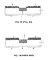
- FIGS. 1A and 1B illustrate silicon contacts formed by conventional RTA/AR etching processes. Specifically, silicide contacts 3 and 5, which preferably contain nickel silicide and platinum silicide, are formed over a semiconductor substrate 1 that includes two silicon-containing semiconductor device regions 2 and 4 with a dielectric isolation region 6 therebetween.
- the present invention provides a method as claimed in claim 1.
- substantially smooth surface refers to a surface that contains little or no surface damage and is characterized by surface protrusions and/or recesses of less than 1 nm in height.
- the present invention provides an improved salicidation method for forming self-aligned silicide contacts over device regions contained by a semiconductor substrate, while completely eliminating formation of residual materials over dielectric isolation regions located between the device regions, as well as minimizing the etching damages to the silicide contacts.
- the resulting structure contains dielectric isolation regions that are essentially free of undesired residual materials (e.g., metal or metal silicide), and the silicide contacts are characterized by a substantially smooth surface.
- FIGS. 2-7 The exemplary processing steps of the present invention will now be described in greater detail by referring to the accompanying FIGS. 2-7 .
- FIG. 2 shows a semiconductor substrate 10 that contains at least two device regions 12 and 14 that are isolated from each other by a dielectric isolation region 16.
- the semiconductor substrate 10 employed in the present invention may comprise any semiconductor material including, but not limited to: undoped Si, n-doped Si, p-doped Si, single crystal Si, polycrystalline Si, amorphous Si, Ge, SiGe, SiC, SiGeC, Ga, GaAs, InAs, InP and all other III/V or II/VI compound semiconductors.
- Semiconductor substrate 10 may also comprise an organic semiconductor or a layered semiconductor such as Si/SiGe, a silicon-on-insulator (SOI) or a SiGe-on-insulator (SGOI).
- the semiconductor substrate 10 is composed of a Si-containing semiconductor material, i.e., a semiconductor material that includes silicon, such as Si (including undoped Si, n-doped Si, p-doped Si, single crystal Si, polycrystalline Si, and amorphous Si), SiGe, SiGeC, etc.
- the silicon contained in the semiconductor substrate 10 can react with the silicide metal subsequently deposited to form the silicide contact.
- the semiconductor substrate 10 may not comprise silicon, and a patterned silicon-containing layer (not shown) is subsequently formed over the semiconductor substrate 10 to selectively cover the device regions 12 and 14, but not the dielectric isolation region 16. In this manner, the subsequently formed patterned silicon-containing layer provides the required silicon for forming the silicide contacts.
- the semiconductor substrate 10 may be doped, undoped or contain both doped and undoped regions therein. These doped regions are known as "wells" and can be used to define various device regions.
- the device region 12 may represent a first doped (n- or p-) region
- the device region 14 may represent a second doped (p- or n-) region, with either the same or different conductivities and/or doping concentrations.
- n-doped regions are used for forming p-channel field effect transistors (p-FETs), and p-doped regions are used for forming n-channel field effect transistors (n-FETs).
- the device regions 12 and 14 may both be n-FET or p-FET device regions, or one of these two regions 12 and 14 is an n-FET region while the other is a p-FET region.
- one of the device regions 12 and 14 is an n-FET region, and the other is a p-FET region.
- the semiconductor substrate 10 is a hybrid substrate, which comprising at least one region (e.g., the n-FET device region) in which mobility of electrons is enhanced, and another region (e.g., the p-FET device region) in which mobility of holes is enhanced.
- the n-FET device region in which mobility of electrons is enhanced
- the p-FET device region in which mobility of holes is enhanced.
- the semiconductor substrate 10 is a hybrid substrate that comprises different regions of different crystal orientations (which is referred to herein as a hybrid crystal orientation substrate).
- Functionality of such hybrid crystal orientation substrates is based on the anisotropy of carrier mobility in the semiconductor crystals.
- the mobility of charged carries such as electrons and holes varies with the crystal orientation of the semiconductor substrate. For example, hole mobility is enhanced for a (110) surface in comparison to a (100) surface in silicon substrate, but electron mobility is enhanced for the (100) silicon surface as compared to the (110) surface.
- the mobility of the respective charge carriers (i.e., either electrons or holes) in the n-FET and p-FET device regions are both enhanced.
- At least one dielectric isolation region 16 is typically provided in the semiconductor substrate 10 to isolate the adjacent device regions 12 and 14 from each other.
- the dielectric isolation region 16 may be a trench isolation region or a field oxide isolation region.
- the trench isolation region is formed utilizing a conventional trench isolation process well known to those skilled in the art. For example, lithography, etching and filling of the trench with a trench dielectric may be used in forming the trench isolation region.
- a liner may be formed in the trench prior to trench fill, a densification step may be performed after the trench fill and a planarization process may follow the trench fill as well.
- the field oxide may be formed utilizing a so-called local oxidation of silicon process.
- the device regions 12 and 14 may each comprise a gate stack (not shown) that includes at least a gate dielectric layer, a gate conductor, and optionally one or more sidewall spacers along the sidewalls of the gate conductor.
- the gate conductor may be a metallic gate conductor, a polysilicon gate conductor, or a gate conductor that comprises both metallic and polysilicon materials, either as a mixture or in separate layers.
- a metal alloy layer 20 is deposited over the semiconductor substrate 10, as shown in FIG. 3 .
- the metal alloy layer 20 comprises nickel alloyed with platinum and, optionally, at least one other metal.
- the total nickel content in the metal alloy layer 20 may range from about 50 to about 95 atomic %, with about 75 to 95 atomic % being more typical.
- the other metal(s) contained by the metal alloy layer 20 is preferably not more than about 50 atomic % but not less than about 5 atomic %, with about 10 to 20 atomic % being more typical.
- the metal alloy layer 20 comprises a nickel-platinum alloy, which can be formed by either depositing a mixture of nickel and platinum, or by first depositing a nickel layer and then incorporating platinum into the nickel layer. Platinum can be readily incorporated into the nickel layer by well-known techniques such as gas phase doping or ion implantation.
- the metal alloy layer 20 may further comprise one or more additional metals selected from the group consisting of Pd, Rh, Ti, V, Cr, Zr, Nb, Mo, Hf, Ta, W, Re, and combinations thereof.
- the additional metal is Re.
- the metal alloy layer preferably has a thickness ranging from about 1 nm to about 40 nm, more preferably from about 2 nm to about 20 nm, and most preferably from about 5 nm to about 15 nm.
- capping layer(s) may be optionally deposited over the metal alloy layer 20.
- Such capping layer(s) comprises at least one material selected from the group consisting of Ti, TiN, W, WN, Ta, and TaN, and it functions to protect the metal alloy layer 20 as well as the silicide contacts to be formed from the metal alloy layer 20.
- a first annealing step is carried out at a relatively low annealing temperature, which ranges from about 150°C to about 500°C using either a continuous heating regime or various ramp and soak heating cycles, for a duration ranging from about 1 second to about 1000 seconds. More preferably, the first annealing step is carried out at an annealing temperature ranging from about 200°C to about 400°C and for a duration ranging from about 5 seconds to about 500 seconds, and most preferably, it is carried out at an annealing temperature ranging from about 250°C to about 350°C and for a duration from about 10 seconds to about 100 seconds.
- a relatively low annealing temperature which ranges from about 150°C to about 500°C using either a continuous heating regime or various ramp and soak heating cycles, for a duration ranging from about 1 second to about 1000 seconds. More preferably, the first annealing step is carried out at an annealing temperature ranging from about 200°C to about 400°C and for a duration ranging from about 5 seconds
- the first annealing step is initiated by raising the surrounding temperature of the entire structure from ambient temperature to the desired annealing temperature at a ramp rate from about 1°C/second to about 35°C/second, more preferably from about 5°C/second to about 25°C/second, and most preferably from about 10°C/second to about 20°C/second. Further, it is preferred that the first annealing step is terminated by lowering the surrounding temperature of the entire structure to below 100°C within a time period from about 10 seconds to about 1000 seconds.
- the first annealing step as described hereinabove is hereby referred to as a low-temperature rapid thermal annealing (RTA) step.
- RTA rapid thermal annealing
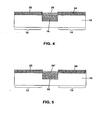
- nickel contained in the portions of the metal alloy layer 20 that are located directly over the first and second device regions 12 and 14 of the semiconductor substrate 10 react with silicon contained in the device regions 12 and 14 to form self-aligned silicide contacts 22 and 24, while the portion 26 of the metal alloy layer 20, which is located directly over the dielectric isolation region 16, contains unreacted nickel, as shown in FIG. 4 .
- the self-aligned silicide contacts 22 and 24 contain at least Ni 2 Si, which is formed by reaction between nickel and silicon at the relatively low annealing temperature and is characterized by a relatively higher resistivity in comparison with NiSi.
- the self-aligned silicide contacts 22 and 24 further contain platinum, which cannot react with silicon to form silicide at the low annealing temperature.
- a nickel-only etching step is carried out to remove substantially all un-reacted nickel, but not the un-reacted platinum, from the portion 26 of the metal alloy layer 20 that is located directly over the dielectric isolation region 16, to form a portion 26' that contains only residual platinum stringers, as shown in FIG. 5 .
- Such nickel-only etching step does not remove nickel silicide (i.e., Ni 2 Si at this point) from the self-aligned silicide contacts 22 and 24. Therefore, the self-aligned silicide contacts 22 and 24 remain substantially intact.
- the nickel-only etching step is carried out by using an etching solution that contains one or more oxidizers selected from the group consisting of hydrogen peroxide, sulfuric acid, potassium permanganate, ferric chloride, persulfate (e.g., ammonium persulfate, sodium persulfate, or potassium persulfate), nitric acid, a ceric compound (such as, for example, ceric ammonium nitrate), etc.
- the nickel-only etching step is carried out using a solution that contains from about 1% to 30% by volume of hydrogen peroxide and from about 10% to about 90% by volume of sulfuric acid.
- a second annealing step is carried out at a relatively high annealing temperature, which ranges from about 300°C to about 600°C using either a continuous heating regime or various ramp and soak heating cycles, for a duration ranging from about 1 second to about 600 seconds. More preferably, the first annealing step is carried out at an annealing temperature ranging from about 350°C to about 550°C and for a duration ranging from about 5 seconds to about 500 seconds, and most preferably, it is carried out at an annealing temperature ranging from about 400°C to about 500°C and for a duration from about 10 seconds to about 100 seconds.
- the second annealing step is initiated by raising the surrounding temperature of the entire structure from ambient temperature to the desired annealing temperature at a ramp rate from about 1°C/second to about 35°C/second, more preferably from about 5°C/second to about 25°C/second, and most preferably from about 10°C/second to about 20°C/second. Further, it is preferred that the second annealing step is terminated by lowering the surrounding temperature of the entire structure to below 100°C within a time period from about 10 seconds to about 600 seconds.
- the second annealing step as described hereinabove is hereby referred to as a high-temperature rapid thermal annealing (RTA) step.
- RTA rapid thermal annealing
- Ni 2 Si contained in the self-aligned silicide contacts 22 and 24 further reacts with silicon in the first and second device regions 12 and 14 of the semiconductor substrate 10 to form completely silicidated and self-aligned contacts 32 and 34 (as shown in FIG. 6 ), which contain NiSi that is characterized by a relatively lower resistivity than Ni 2 Si.
- the unreacted platinum contained in the self-aligned silicide contacts 22 and 24 reacts with silicon in the first and second device regions 12 and 14 at the high annealing temperature, to form platinum silicide in the contacts 32 and 34, while the platinum stringers contained by the portion 26' located directly over the dielectric isolation region 16 remain unreacted (due to lack of silicon in the region 16), as shown in FIG. 6 .
- a second etching step is carried out to remove substantially all the unreacted platinum stringers contained by the portion 26' in selection over the NiSi and PtSi contained by the self-aligned silicide contacts 32 and 34, thereby exposing the dielectric isolation region 16 but without damaging the self-aligned silicide contacts 32 and 34.
- the second etching step is carried out by using an etching solution that contains at least one oxidizing agent, at least one complexing agent, and at least one solvent.
- the molar ratio of the oxidizing agent(s), the complexing agent(s), and the solvent(s) in the second etching solution preferably ranges from about 1:10:200 to about 1:1:5.
- the at least one oxidizing agent used in the second etching step can be selected from the group consisting of nitric acid, hydrogen peroxide, potassium permanganate, sodium persulfate, ammonia persulfate, potassium persulfate, ceric ammonium nitriate, potassium monopersulfate, etc. More preferably, the oxidizing agent is nitric acid.
- the at least one complexing agent functions to form a complex with noble metal ions, such as platinum ions or gold ions, so as to facilitate etching of the noble metal(s).
- a complexing agent comprises halogen ions from at least one compound selected from the group consisting of sodium chloride, hydrochloric acid, sodium iodide, potassium iodide, sodium bromide, and potassium bromide. More preferably, the complexing agent comprises hydrochloric acid.
- the at least one solvent contained by the second etching solution can be either a polar solvent or a non-polar solvent, and preferably the solvent contains at least water.
- the second etching solution is an aqua regia (AR) solution that comprises nitric acid as the oxidizing agent, hydrochloric acid as the complexing agent, and water as the solvent. More preferably, the AR solution comprises from about 40% to about 80% by volume of nitric acid, from about 20% to about 60% by volume of hydrochloric acid, and the remaining balance of water.
- AR aqua regia
- the second etching step is preferably carried out at an etching temperature ranging from about 30°C to about 80°C for a duration ranging from about 3 minutes to about 45 minutes. More preferably, the second etching step is carried out at an etching temperature ranging from about 35°C to about 45°C for a duration of from about 15 minutes to about 45 minutes.
- the etching solution Prior to the etching (i.e., prior to the contact of the etching solution with the structure to be etched), it is preferred that the etching solution is maintained at an elevated temperature from about 30°C to about 80°C for a duration of at least about 10 minutes, more preferably at lest about 15 minutes. Further, after the etching (i.e., after removal of the structure from the etching solution), it is preferred that the structure is rinsed and then dried to remove trace amount of the etching solution.
- the second etching step effectively removes substantially all the unreacted platinum stringers from the upper surface of the dielectric isolation region 16, without attacking or otherwise damaging the NiSi and PtSi contained by the silicide contacts 32 and 34.
- both the first and second annealing steps are preferably carried out in a gas atmosphere, e.g., He, Ar, N 2 or forming gas. They may be carried out in different atmospheres or in the same atmosphere.
- He may be used in both annealing steps, or He can be used in the first annealing step and a forming gas may be used in the second annealing step.
- One unique aspect of the present invention is the use of two different etching solutions in two separate etching steps to remove the unreacted silicide metals (i.e., nickel and platinum).
- the first etching step which follows the low-temperature RTA step, removes the bulk amount of the unreacted nickel from the upper surface of the dielectric isolation region 16.
- the second, more aggressive etching step which follows the high-temperature RTA step, then removes the platinum stringers or other hard-to-remove alloying metal(s) from the upper surface of the dielectric isolation region 16.
- the high-temperature RTA step which proceeds the second etching step, functions to effectively convert the metals contacted by the silicide contacts 32 and 34 over the device regions 12 and 14 into complete silicide (such as NiSi and PtSi) that are resistant to attacks by the second etching step.
- the exposed dielectric isolation region 16 is essentially free of metal and metal silicide, while the self-aligned silicide contacts 32 and 34 are substantially undamaged and are characterized by a substantially smooth surface morphology (i.e., having surface protrusions and/or recesses of less than 1 nm in height), as shown in FIG. 7 .
- the second etching step as described hereinabove can also be used separately (i.e., independent of the RTA steps and the first etching step) for selective etching of nickel-platinum alloy over nickel silicide and platinum silicide.
- an etching bath comprising at least one oxidizing agent, at least one complexing agent, and at least one solvent, as described hereinabove, is first provided and maintained at an elevated temperature ranging from about 30°C to about 80°C for at least 15 minutes.
- a work piece that comprises nickel-platinum alloy, nickel silicide, and platinum silicide is contacted with the etching bath at an etching temperature ranging from about 30°C to about 80°C for a duration of from about 10 to about 45 minutes.
- the work piece is removed from the etching bath, and then rinsed and dried to remove traces of the etchants from the work piece.
- the substrate 10 may also comprise silicon-containing semiconductor alloys (eg., SiGe or SiC) for formation of other metal-semiconductor alloys (e.g., NiGe, NiC, PtGe, and/or PtC) in conjunction with the metal silicides.
- SiGe or SiC silicon-containing semiconductor alloys
- other metal-semiconductor alloys e.g., NiGe, NiC, PtGe, and/or PtC
- FIGS. 2-7 illustratively demonstrates exemplary processing steps that can be used to form self-aligned silicide contacts isolated from each other by an exposed dielectric region, according to a specific embodiment of the present invention, it is clear that a person ordinarily skilled in the art can readily modify such processing steps for adaptation to specific application requirements, consistent with the above descriptions.
Landscapes
- Chemical & Material Sciences (AREA)
- Chemical Kinetics & Catalysis (AREA)
- General Chemical & Material Sciences (AREA)
- Engineering & Computer Science (AREA)
- Materials Engineering (AREA)
- Mechanical Engineering (AREA)
- Metallurgy (AREA)
- Organic Chemistry (AREA)
- Electrodes Of Semiconductors (AREA)
- Internal Circuitry In Semiconductor Integrated Circuit Devices (AREA)
Description
- The present invention generally relates to a method for forming self-aligned metal silicide contacts for semiconductor devices. More specifically, the present invention relates to a method for forming self-aligned metal silicide contacts for at least two silicon-containing semiconductor regions that are spaced apart from each other by an exposed dielectric region.
- The technological development of micro-sized semiconductor integrated circuit devices has required improved methods for making conductive contacts to the semiconductor impurity regions. Metal silicides have proven to be excellent contact materials, which can be readily formed in a self-aligned manner by a salicidation process.
- Formation of metal silicide contacts through the salicidation process typically involves the steps of depositing a thin metal layer (e.g., less than about 15 nm in thickness) that contains a silicide metal or metal alloy (i.e., a metal or metal alloy that is capable of reacting with silicon to form metal silicide) uniformly over a semiconductor substrate that contains both silicon-containing device regions and dielectric isolation regions, heating the semiconductor substrate to form silicide over the device regions, and then selectively etching away the unreacted metal from the dielectric isolation regions. For successful fabrication of high performance semiconductor devices, the etching should be highly selective, i.e., it removes all unreacted metal or metal alloy from the dielectric isolation regions, without attacking or otherwise damaging the silicide on the device regions.
- Nickel or nickel alloy, such as nickel-platinum alloy, have been commonly used as the silicide metal for forming the silicide contacts in the CMOS technology.
- Specifically, for forming pure nickel silicide contacts, a rapid thermal annealing (RTA) step is typically employed to convert the deposited thin nickel layer located on the device regions into nickel silicide, followed by a nickel-etching step to remove the unreacted nickel from the dielectric isolation regions. However, residual material, probably nickel silicide, tends to form over the dielectric isolation regions after the RTA step. Such residual material cannot be satisfactorily removed by the etchant(s) used in the nickel-etching step. The presence of residue material on the dielectric isolation region significantly increases the risk of shorting between device regions and reduces the device reliability. This problem becomes more severe as the RTA temperature increases.
- Further, for forming silicide contacts that contain nickel silicide as well as one or more other metal silicides, such as platinum silicide and/or rhenium silicide, a nickel alloy layer that contains nickel and one or more additional silicide metals, such as platinum and/or rhenium, is deposited over the semiconductor substrate. An RTA step is also employed to convert nickel and platinum/rhenium into nickel silicide and platinum/rhenium silicide in the device regions, followed by an aqua regia (AR) etching step to remove both the unreacted nickel and platinum/rhenium from the dielectric isolation regions. Similar problem exists due to presence of residual material over the dielectric isolation regions after the RTA step.
- Moreover, when the RTA temperature equals or is less than about 400°C, the silicides formed by the RTA is highly susceptible to attacks by the AR etchant, and significant damages to the silicide contacts may result during the AR etching. On the other hand, when the RTA is carried out at a higher temperature (e.g., >600°C), gross formation of residual material is observed over the dielectric isolation regions.
FIGS. 1A and 1B illustrate silicon contacts formed by conventional RTA/AR etching processes. Specifically,silicide contacts 3 and 5, which preferably contain nickel silicide and platinum silicide, are formed over asemiconductor substrate 1 that includes two silicon-containingsemiconductor device regions dielectric isolation region 6 therebetween. When the RTA temperature is not high enough, thesilicide contacts 3 and 5 will be severely damaged by the AR etching, thereby resulting in a very irregular surface morphology, as shown inFIG. 1A . On the other hand, when the RTA temperature is higher, residual materials (e.g., nickel-platinum-silicide), which are denoted bylayer 7, can be formed over thedielectric isolation region 6, as shown inFIG. 1B . -
US 2005/158996 andUS 2006/051961 describe a method of forming self-aligned nickel silicide contacts including depositing a Ni Pt alloy. - There is therefore a continuing need for an improved method for fabricating the silicide contacts on semiconductor substrates, which is capable of both minimizing the formation of residual materials on the dielectric isolation regions and reducing etching damages to the silicide contacts.
- The present invention provides a method as claimed in
claim 1. - The term "substantially smooth surface" as used herein refers to a surface that contains little or no surface damage and is characterized by surface protrusions and/or recesses of less than 1 nm in height.
- Other aspects, features and advantages of the invention will be more fully apparent from the ensuing disclosure and appended claims.
-
-
FIGS. 1A and 1B show silicide contacts formed over a semiconductor substrate by conventional RTA/AR etching processes. -
FIGS. 2-7 show exemplary processing steps for forming silicide contacts over a semiconductor substrate, according to one embodiment of the present invention. - In the following description, numerous specific details are set forth, such as particular structures, components, materials, dimensions, processing steps and techniques, in order to provide a thorough understanding of the present invention. However, it will be appreciated by one of ordinary skill in the art that the invention may be practiced without these specific details. In other instances, well-known structures or processing steps have not been described in detail in order to avoid obscuring the invention.
- It will be understood that when an element as a layer, region or substrate is referred to as being "on" or "over" another element, it can be directly on the other element or intervening elements may also be present. In contrast, when an element is referred to as being "directly on" or "directly over" another element, there are no intervening elements present. It will also be understood that when an element is referred to as being "connected" or "coupled" to another element, it can be directly connected or coupled to the other element or intervening elements may be present. In contrast, when an element is referred to as being "directly connected" or "directly coupled" to another element, there are no intervening elements present.
- The present invention provides an improved salicidation method for forming self-aligned silicide contacts over device regions contained by a semiconductor substrate, while completely eliminating formation of residual materials over dielectric isolation regions located between the device regions, as well as minimizing the etching damages to the silicide contacts. The resulting structure contains dielectric isolation regions that are essentially free of undesired residual materials (e.g., metal or metal silicide), and the silicide contacts are characterized by a substantially smooth surface.
- The exemplary processing steps of the present invention will now be described in greater detail by referring to the accompanying
FIGS. 2-7 . - Reference is first made to
FIG. 2 , which shows asemiconductor substrate 10 that contains at least twodevice regions dielectric isolation region 16. - The
semiconductor substrate 10 employed in the present invention may comprise any semiconductor material including, but not limited to: undoped Si, n-doped Si, p-doped Si, single crystal Si, polycrystalline Si, amorphous Si, Ge, SiGe, SiC, SiGeC, Ga, GaAs, InAs, InP and all other III/V or II/VI compound semiconductors.Semiconductor substrate 10 may also comprise an organic semiconductor or a layered semiconductor such as Si/SiGe, a silicon-on-insulator (SOI) or a SiGe-on-insulator (SGOI). - In preferred embodiments of the present invention, the
semiconductor substrate 10 is composed of a Si-containing semiconductor material, i.e., a semiconductor material that includes silicon, such as Si (including undoped Si, n-doped Si, p-doped Si, single crystal Si, polycrystalline Si, and amorphous Si), SiGe, SiGeC, etc. The silicon contained in thesemiconductor substrate 10 can react with the silicide metal subsequently deposited to form the silicide contact. On the other hand, it is also contemplated by the present invention that thesemiconductor substrate 10 may not comprise silicon, and a patterned silicon-containing layer (not shown) is subsequently formed over thesemiconductor substrate 10 to selectively cover thedevice regions dielectric isolation region 16. In this manner, the subsequently formed patterned silicon-containing layer provides the required silicon for forming the silicide contacts. - The
semiconductor substrate 10 may be doped, undoped or contain both doped and undoped regions therein. These doped regions are known as "wells" and can be used to define various device regions. For example, thedevice region 12 may represent a first doped (n- or p-) region, and thedevice region 14 may represent a second doped (p- or n-) region, with either the same or different conductivities and/or doping concentrations. Typically, n-doped regions are used for forming p-channel field effect transistors (p-FETs), and p-doped regions are used for forming n-channel field effect transistors (n-FETs). Therefore, thedevice regions regions device regions - In a particularly preferred embodiment of the present invention, the
semiconductor substrate 10 is a hybrid substrate, which comprising at least one region (e.g., the n-FET device region) in which mobility of electrons is enhanced, and another region (e.g., the p-FET device region) in which mobility of holes is enhanced. By fabricating the n-FET in the electron-mobility-enhanced region and the p-FET in the hole-mobility-enhanced region, the mobility of the respective charge carriers (i.e., either electrons or holes) in the n-FET and p-FET device regions can simultaneously be enhanced, thereby improving the complementary metal-oxide-semiconductor (CMOS) device performance. - More specifically, the
semiconductor substrate 10 is a hybrid substrate that comprises different regions of different crystal orientations (which is referred to herein as a hybrid crystal orientation substrate). Functionality of such hybrid crystal orientation substrates is based on the anisotropy of carrier mobility in the semiconductor crystals. Specifically, the mobility of charged carries such as electrons and holes varies with the crystal orientation of the semiconductor substrate. For example, hole mobility is enhanced for a (110) surface in comparison to a (100) surface in silicon substrate, but electron mobility is enhanced for the (100) silicon surface as compared to the (110) surface. Therefore, by fabricating the n-FET in a device region having the (100) surface crystal orientation, and the p-FET in a different device region having the (110) surface crystal orientation, the mobility of the respective charge carriers (i.e., either electrons or holes) in the n-FET and p-FET device regions are both enhanced. - At least one
dielectric isolation region 16 is typically provided in thesemiconductor substrate 10 to isolate theadjacent device regions dielectric isolation region 16 may be a trench isolation region or a field oxide isolation region. The trench isolation region is formed utilizing a conventional trench isolation process well known to those skilled in the art. For example, lithography, etching and filling of the trench with a trench dielectric may be used in forming the trench isolation region. Optionally, a liner may be formed in the trench prior to trench fill, a densification step may be performed after the trench fill and a planarization process may follow the trench fill as well. The field oxide may be formed utilizing a so-called local oxidation of silicon process. - The
device regions - A
metal alloy layer 20 is deposited over thesemiconductor substrate 10, as shown inFIG. 3 . Themetal alloy layer 20 comprises nickel alloyed with platinum and, optionally, at least one other metal. The total nickel content in themetal alloy layer 20 may range from about 50 to about 95 atomic %, with about 75 to 95 atomic % being more typical. The other metal(s) contained by themetal alloy layer 20 is preferably not more than about 50 atomic % but not less than about 5 atomic %, with about 10 to 20 atomic % being more typical. - Preferably, the
metal alloy layer 20 comprises a nickel-platinum alloy, which can be formed by either depositing a mixture of nickel and platinum, or by first depositing a nickel layer and then incorporating platinum into the nickel layer. Platinum can be readily incorporated into the nickel layer by well-known techniques such as gas phase doping or ion implantation. Themetal alloy layer 20 may further comprise one or more additional metals selected from the group consisting of Pd, Rh, Ti, V, Cr, Zr, Nb, Mo, Hf, Ta, W, Re, and combinations thereof. Preferably, the additional metal is Re. The metal alloy layer preferably has a thickness ranging from about 1 nm to about 40 nm, more preferably from about 2 nm to about 20 nm, and most preferably from about 5 nm to about 15 nm. - One or more capping layers (not shown) may be optionally deposited over the
metal alloy layer 20. Such capping layer(s) comprises at least one material selected from the group consisting of Ti, TiN, W, WN, Ta, and TaN, and it functions to protect themetal alloy layer 20 as well as the silicide contacts to be formed from themetal alloy layer 20. - Next, a first annealing step is carried out at a relatively low annealing temperature, which ranges from about 150°C to about 500°C using either a continuous heating regime or various ramp and soak heating cycles, for a duration ranging from about 1 second to about 1000 seconds. More preferably, the first annealing step is carried out at an annealing temperature ranging from about 200°C to about 400°C and for a duration ranging from about 5 seconds to about 500 seconds, and most preferably, it is carried out at an annealing temperature ranging from about 250°C to about 350°C and for a duration from about 10 seconds to about 100 seconds. In a particularly preferred embodiment, the first annealing step is initiated by raising the surrounding temperature of the entire structure from ambient temperature to the desired annealing temperature at a ramp rate from about 1°C/second to about 35°C/second, more preferably from about 5°C/second to about 25°C/second, and most preferably from about 10°C/second to about 20°C/second. Further, it is preferred that the first annealing step is terminated by lowering the surrounding temperature of the entire structure to below 100°C within a time period from about 10 seconds to about 1000 seconds.
- The first annealing step as described hereinabove is hereby referred to as a low-temperature rapid thermal annealing (RTA) step. As a result of such a low-temperature RTA step, nickel contained in the portions of the
metal alloy layer 20 that are located directly over the first andsecond device regions semiconductor substrate 10 react with silicon contained in thedevice regions silicide contacts portion 26 of themetal alloy layer 20, which is located directly over thedielectric isolation region 16, contains unreacted nickel, as shown inFIG. 4 . The self-alignedsilicide contacts silicide contacts - After the low-temperature RTA step, a nickel-only etching step is carried out to remove substantially all un-reacted nickel, but not the un-reacted platinum, from the
portion 26 of themetal alloy layer 20 that is located directly over thedielectric isolation region 16, to form a portion 26' that contains only residual platinum stringers, as shown inFIG. 5 . Such nickel-only etching step does not remove nickel silicide (i.e., Ni2Si at this point) from the self-alignedsilicide contacts silicide contacts - Preferably, the nickel-only etching step is carried out by using an etching solution that contains one or more oxidizers selected from the group consisting of hydrogen peroxide, sulfuric acid, potassium permanganate, ferric chloride, persulfate (e.g., ammonium persulfate, sodium persulfate, or potassium persulfate), nitric acid, a ceric compound (such as, for example, ceric ammonium nitrate), etc. In a preferred embodiment of the present invention, the nickel-only etching step is carried out using a solution that contains from about 1% to 30% by volume of hydrogen peroxide and from about 10% to about 90% by volume of sulfuric acid.
- Subsequently, a second annealing step is carried out at a relatively high annealing temperature, which ranges from about 300°C to about 600°C using either a continuous heating regime or various ramp and soak heating cycles, for a duration ranging from about 1 second to about 600 seconds. More preferably, the first annealing step is carried out at an annealing temperature ranging from about 350°C to about 550°C and for a duration ranging from about 5 seconds to about 500 seconds, and most preferably, it is carried out at an annealing temperature ranging from about 400°C to about 500°C and for a duration from about 10 seconds to about 100 seconds. In a particularly preferred embodiment, the second annealing step is initiated by raising the surrounding temperature of the entire structure from ambient temperature to the desired annealing temperature at a ramp rate from about 1°C/second to about 35°C/second, more preferably from about 5°C/second to about 25°C/second, and most preferably from about 10°C/second to about 20°C/second. Further, it is preferred that the second annealing step is terminated by lowering the surrounding temperature of the entire structure to below 100°C within a time period from about 10 seconds to about 600 seconds.
- The second annealing step as described hereinabove is hereby referred to as a high-temperature rapid thermal annealing (RTA) step. As a result of such a high-temperature RTA step, Ni2Si contained in the self-aligned
silicide contacts second device regions semiconductor substrate 10 to form completely silicidated and self-alignedcontacts 32 and 34 (as shown inFIG. 6 ), which contain NiSi that is characterized by a relatively lower resistivity than Ni2Si. Further, the unreacted platinum contained in the self-alignedsilicide contacts second device regions contacts dielectric isolation region 16 remain unreacted (due to lack of silicon in the region 16), as shown inFIG. 6 . - After the high-temperature RTA step, a second etching step is carried out to remove substantially all the unreacted platinum stringers contained by the portion 26' in selection over the NiSi and PtSi contained by the self-aligned
silicide contacts dielectric isolation region 16 but without damaging the self-alignedsilicide contacts - The second etching step is carried out by using an etching solution that contains at least one oxidizing agent, at least one complexing agent, and at least one solvent. The molar ratio of the oxidizing agent(s), the complexing agent(s), and the solvent(s) in the second etching solution preferably ranges from about 1:10:200 to about 1:1:5.
- The at least one oxidizing agent used in the second etching step can be selected from the group consisting of nitric acid, hydrogen peroxide, potassium permanganate, sodium persulfate, ammonia persulfate, potassium persulfate, ceric ammonium nitriate, potassium monopersulfate, etc. More preferably, the oxidizing agent is nitric acid.
- The at least one complexing agent functions to form a complex with noble metal ions, such as platinum ions or gold ions, so as to facilitate etching of the noble metal(s). Preferably, such a complexing agent comprises halogen ions from at least one compound selected from the group consisting of sodium chloride, hydrochloric acid, sodium iodide, potassium iodide, sodium bromide, and potassium bromide. More preferably, the complexing agent comprises hydrochloric acid.
- The at least one solvent contained by the second etching solution can be either a polar solvent or a non-polar solvent, and preferably the solvent contains at least water.
- In a preferred embodiment of the present invention, the second etching solution is an aqua regia (AR) solution that comprises nitric acid as the oxidizing agent, hydrochloric acid as the complexing agent, and water as the solvent. More preferably, the AR solution comprises from about 40% to about 80% by volume of nitric acid, from about 20% to about 60% by volume of hydrochloric acid, and the remaining balance of water.
- The second etching step is preferably carried out at an etching temperature ranging from about 30°C to about 80°C for a duration ranging from about 3 minutes to about 45 minutes. More preferably, the second etching step is carried out at an etching temperature ranging from about 35°C to about 45°C for a duration of from about 15 minutes to about 45 minutes. Prior to the etching (i.e., prior to the contact of the etching solution with the structure to be etched), it is preferred that the etching solution is maintained at an elevated temperature from about 30°C to about 80°C for a duration of at least about 10 minutes, more preferably at lest about 15 minutes. Further, after the etching (i.e., after removal of the structure from the etching solution), it is preferred that the structure is rinsed and then dried to remove trace amount of the etching solution.
- The second etching step effectively removes substantially all the unreacted platinum stringers from the upper surface of the
dielectric isolation region 16, without attacking or otherwise damaging the NiSi and PtSi contained by thesilicide contacts - Note that both the first and second annealing steps are preferably carried out in a gas atmosphere, e.g., He, Ar, N2 or forming gas. They may be carried out in different atmospheres or in the same atmosphere. For example, He may be used in both annealing steps, or He can be used in the first annealing step and a forming gas may be used in the second annealing step.
- One unique aspect of the present invention is the use of two different etching solutions in two separate etching steps to remove the unreacted silicide metals (i.e., nickel and platinum). The first etching step, which follows the low-temperature RTA step, removes the bulk amount of the unreacted nickel from the upper surface of the
dielectric isolation region 16. The second, more aggressive etching step, which follows the high-temperature RTA step, then removes the platinum stringers or other hard-to-remove alloying metal(s) from the upper surface of thedielectric isolation region 16. More importantly, the high-temperature RTA step, which proceeds the second etching step, functions to effectively convert the metals contacted by thesilicide contacts device regions - Correspondingly, the exposed
dielectric isolation region 16 is essentially free of metal and metal silicide, while the self-alignedsilicide contacts FIG. 7 . - The second etching step as described hereinabove can also be used separately (i.e., independent of the RTA steps and the first etching step) for selective etching of nickel-platinum alloy over nickel silicide and platinum silicide. Specifically, an etching bath comprising at least one oxidizing agent, at least one complexing agent, and at least one solvent, as described hereinabove, is first provided and maintained at an elevated temperature ranging from about 30°C to about 80°C for at least 15 minutes. Next, a work piece that comprises nickel-platinum alloy, nickel silicide, and platinum silicide is contacted with the etching bath at an etching temperature ranging from about 30°C to about 80°C for a duration of from about 10 to about 45 minutes. Thereafter, the work piece is removed from the etching bath, and then rinsed and dried to remove traces of the etchants from the work piece.
- It is important to note that although the description hereinabove is focused primarily on formation of metal silicides on a
silicon substrate 10, it is readily understood that thesubstrate 10 may also comprise silicon-containing semiconductor alloys (eg., SiGe or SiC) for formation of other metal-semiconductor alloys (e.g., NiGe, NiC, PtGe, and/or PtC) in conjunction with the metal silicides. For example, when SiGe is used as the substrate material in thesemiconductor substrate 10, NiGe will be formed together with NiSi. The methods of the present invention are equally applicable to such semiconductor alloys. - While
FIGS. 2-7 illustratively demonstrates exemplary processing steps that can be used to form self-aligned silicide contacts isolated from each other by an exposed dielectric region, according to a specific embodiment of the present invention, it is clear that a person ordinarily skilled in the art can readily modify such processing steps for adaptation to specific application requirements, consistent with the above descriptions.
Claims (13)
- A method for forming a semiconductor structure comprising:providing a semiconductor substrate (10) including a first device region (12) comprising a silicon-containing semiconductor material, a second device region (14) comprising said silicon-containing semiconductor material, and a dielectric isolation region (16) laterally abutting said first device region and said second device region and located in said semiconductor substrate;forming a metal alloy layer (20) over said first device region and said second device region and said dielectric isolation region, wherein said metal alloy layer comprises nickel and platinum;annealing at a first annealing temperature ranging from 150°C to 500°C, wherein nickel contained in said metal alloy layer reacts with silicon contained in said first device region and said second device region to form nickel silicide of a first phase over said first device region and said second device region,;selectively etching said metal alloy layer using a first etching solution to remove substantially all un-reacted nickel from said dielectric isolation region between said first device region and said second device region, wherein platinum stringers remain over said dielectric isolation region;annealing at a second annealing temperature ranging from 300°C to 600°C, wherein said nickel silicide of said first phase further reacts with silicon contained in said first device region and said second region to form nickel silicide of a second phase over said first device region and said second device region, wherein the second phase has a lower resistivity than the first phase; andselectively etching said platinum stringers using a second etching solution to remove substantially all of said platinum from an upper surface of said dielectric isolation region, thereby forming self-aligned metal silicide contacts that are electrically isolated from each other.
- The method of claim 1, wherein said first device region and said second device region comprise at least one of undoped Si, n-doped Si, p-doped Si, single crystal Si, polycrystalline Si, amorphous Si, SiGe, SiGeC, and combinations thereof.
- The method of claim 1, wherein said metal alloy layer furher comprises, at least another metal selected from the group consisting of Pd, Rh, Ti, V, Cr, Zr, Nb, Mo, Hf, Ta, W, Re and combinations thereof.
- The method of Claim 3, wherein said another metal is Re.
- The method of Claims 1 or 3, wherein said metal alloy layer comprises from 50 to 95 atomic % of nickel, and up to 50 atomic % of platinum and said at least another metal.
- The method of Claim 1, wherein said metal alloy layer has a thickness ranging from 1 nm to 40 nm.
- The method of Claim 1, further comprising forming a capping layer over said metal alloy layer prior to annealing at said first temperature.
- The method of Claim 7, wherein said capping layer comprises at least one material selected from the group consisting of Ti, TiN, W, WN, Ta and TaN.
- The method of Claim 1, wherein said first etching solution comprises at least one of a peroxide-sulfuric acid solution, a ferric chloride solution, an ammonium persulfate solution, a nitric acid solution, and a ceric solution.
- The method of Claim 1, wherein said second etching solution comprises at least one oxidizing agent, at least one complexing agent, and at least one solvent, and wherein said platinum stringers are contacted with said second etching solution at an etching temperature ranging from 30°C to 80°C for a duration ranging from 3 minutes to 45 minutes, wherein substantially all of said platinum stringers are removed from said dielectric isolation region.
- The method of Claim 10, wherein said platinum stringers are contacted with said second etching solution at an etching temperature ranging from 35°C to 45°C for a duration of from 15 minutes to 45 minutes.
- The method of Claim 10, wherein said at least one oxidizing agent, said at least one complexing agent, and said at least one solvent are present in a molar ratio from 1:10:200 to 1:1:5.
- The method of Claim 10, wherein said at least one oxidizing agent comprises at least one selected from the group consisting of nitric acid, hydrogen peroxide, potassium permanganate, sodium persulfate, ammonia persulfate, potassium persulfate, ceric ammonium nitrate, and potassium monopersulfate.
Applications Claiming Priority (2)
| Application Number | Priority Date | Filing Date | Title |
|---|---|---|---|
| US11/415,922 US7618891B2 (en) | 2006-05-01 | 2006-05-01 | Method for forming self-aligned metal silicide contacts |
| PCT/US2007/008798 WO2007133356A1 (en) | 2006-05-01 | 2007-04-10 | Method for forming self-aligned metal silicide contacts |
Publications (3)
| Publication Number | Publication Date |
|---|---|
| EP2022085A1 EP2022085A1 (en) | 2009-02-11 |
| EP2022085A4 EP2022085A4 (en) | 2011-08-03 |
| EP2022085B1 true EP2022085B1 (en) | 2014-10-15 |
Family
ID=38648852
Family Applications (1)
| Application Number | Title | Priority Date | Filing Date |
|---|---|---|---|
| EP07755161.2A Not-in-force EP2022085B1 (en) | 2006-05-01 | 2007-04-10 | Method for forming self-aligned metal silicide contacts |
Country Status (7)
| Country | Link |
|---|---|
| US (2) | US7618891B2 (en) |
| EP (1) | EP2022085B1 (en) |
| JP (1) | JP5186486B2 (en) |
| KR (1) | KR20090037384A (en) |
| CN (1) | CN101432860B (en) |
| TW (1) | TWI415174B (en) |
| WO (1) | WO2007133356A1 (en) |
Families Citing this family (44)
| Publication number | Priority date | Publication date | Assignee | Title |
|---|---|---|---|---|
| US7618891B2 (en) * | 2006-05-01 | 2009-11-17 | International Business Machines Corporation | Method for forming self-aligned metal silicide contacts |
| US7501333B2 (en) * | 2006-07-19 | 2009-03-10 | Taiwan Semiconductor Manufacturing Co., Ltd. | Work function adjustment on fully silicided (FUSI) gate |
| JP5186701B2 (en) * | 2006-09-25 | 2013-04-24 | 富士通セミコンダクター株式会社 | Manufacturing method of semiconductor device |
| JP5286664B2 (en) * | 2006-11-29 | 2013-09-11 | 富士通セミコンダクター株式会社 | Manufacturing method of semiconductor device |
| FR2912549B1 (en) * | 2007-02-08 | 2009-06-05 | Commissariat Energie Atomique | PROCESS FOR PREPARING A GERMANIUM LAYER FROM A SILICON-GERMANIUM-INSULATING SUBSTRATE |
| JP4759079B2 (en) * | 2008-12-03 | 2011-08-31 | パナソニック株式会社 | Manufacturing method of semiconductor device |
| US9379011B2 (en) * | 2008-12-19 | 2016-06-28 | Asm International N.V. | Methods for depositing nickel films and for making nickel silicide and nickel germanide |
| JP4749471B2 (en) * | 2009-01-13 | 2011-08-17 | パナソニック株式会社 | Manufacturing method of semiconductor device |
| JP2010186984A (en) * | 2009-01-13 | 2010-08-26 | Panasonic Corp | Method for fabricating semiconductor device |
| JP5420345B2 (en) * | 2009-08-14 | 2014-02-19 | ルネサスエレクトロニクス株式会社 | Semiconductor device and manufacturing method thereof |
| US8686562B2 (en) | 2009-08-25 | 2014-04-01 | International Rectifier Corporation | Refractory metal nitride capped electrical contact and method for frabricating same |
| CN102110624B (en) * | 2009-12-23 | 2012-05-30 | 中芯国际集成电路制造(上海)有限公司 | Method for detecting nickel and platinum removing device |
| CN102194674A (en) * | 2010-03-12 | 2011-09-21 | 中芯国际集成电路制造(上海)有限公司 | Manufacturing method for self-aligned metal silicide |
| US20130130500A1 (en) * | 2010-08-05 | 2013-05-23 | Showa Denko K.K. | Composition for removal of nickel-platinum alloy-based metals |
| KR101938022B1 (en) | 2011-03-11 | 2019-01-11 | 후지필름 일렉트로닉 머티리얼스 유.에스.에이., 아이엔씨. | Novel etching composition |
| JP5992150B2 (en) * | 2011-07-08 | 2016-09-14 | 富士フイルム株式会社 | Semiconductor substrate product manufacturing method, thin film removing solution and kit used therefor |
| US8784572B2 (en) * | 2011-10-19 | 2014-07-22 | Intermolecular, Inc. | Method for cleaning platinum residues on a semiconductor substrate |
| TWI577834B (en) | 2011-10-21 | 2017-04-11 | 富士軟片電子材料美國股份有限公司 | Novel passivation composition and method |
| CN103137462B (en) * | 2011-11-25 | 2015-11-25 | 中芯国际集成电路制造(上海)有限公司 | The formation method of self-aligned metal silicate |
| ES2619568T3 (en) | 2011-12-15 | 2017-06-26 | Entegris Inc. | Apparatus and method of extraction of welding metals during the recycling of electrical and electronic waste equipment |
| US9136134B2 (en) * | 2012-02-22 | 2015-09-15 | Soitec | Methods of providing thin layers of crystalline semiconductor material, and related structures and devices |
| US8835318B2 (en) * | 2012-03-08 | 2014-09-16 | Globalfoundries Inc. | HNO3 single wafer clean process to strip nickel and for MOL post etch |
| JP6132082B2 (en) * | 2012-03-30 | 2017-05-24 | 栗田工業株式会社 | Semiconductor substrate cleaning method and cleaning system |
| WO2013170130A1 (en) * | 2012-05-11 | 2013-11-14 | Advanced Technology Materials, Inc. | Formulations for wet etching nipt during silicide fabrication |
| US8927422B2 (en) | 2012-06-18 | 2015-01-06 | International Business Machines Corporation | Raised silicide contact |
| CN102723268A (en) * | 2012-06-20 | 2012-10-10 | 上海华力微电子有限公司 | Method for preparing self-aligned nickel-silicide |
| US9263556B2 (en) * | 2012-06-29 | 2016-02-16 | Taiwan Semiconductor Manufacturing Company, Ltd. | Silicide process using OD spacers |
| CN103579000B (en) * | 2012-08-03 | 2016-09-21 | 中芯国际集成电路制造(上海)有限公司 | A kind of manufacture method of semiconductor device |
| JP5787098B2 (en) | 2012-08-22 | 2015-09-30 | 栗田工業株式会社 | Semiconductor substrate cleaning method and cleaning system |
| US8709277B2 (en) * | 2012-09-10 | 2014-04-29 | Fujifilm Corporation | Etching composition |
| US8835309B2 (en) | 2012-09-13 | 2014-09-16 | International Business Machines Corporation | Forming nickel—platinum alloy self-aligned silicide contacts |
| JP5880860B2 (en) | 2012-10-02 | 2016-03-09 | 栗田工業株式会社 | Semiconductor substrate cleaning method and cleaning system |
| TWI517235B (en) * | 2013-03-01 | 2016-01-11 | 栗田工業股份有限公司 | Semiconductor substrate cleaning system and semiconductor substrate cleaning method |
| JP6003919B2 (en) | 2014-02-10 | 2016-10-05 | トヨタ自動車株式会社 | Semiconductor device and manufacturing method thereof |
| JP2015162653A (en) * | 2014-02-28 | 2015-09-07 | 富士フイルム株式会社 | Etching composition, etching method using the same, and method for manufacturing semiconductor substrate product |
| CN104078344B (en) * | 2014-07-11 | 2017-04-05 | 上海华力微电子有限公司 | The method for reducing autoregistration nickle silicide spike defect and defect of pipeline |
| CN104362087A (en) * | 2014-11-07 | 2015-02-18 | 上海华力微电子有限公司 | Method for forming self-aligned metal silicide |
| WO2016147709A1 (en) * | 2015-03-13 | 2016-09-22 | 奥野製薬工業株式会社 | Electrolytic stripping agent for jig |
| CN106783965A (en) * | 2016-12-01 | 2017-05-31 | 上海华力微电子有限公司 | A kind of germanium silicon source drain electrode and preparation method |
| KR101985167B1 (en) * | 2017-10-31 | 2019-06-04 | 케이피엑스케미칼 주식회사 | Compositions for etching and methods for etching metal using the same |
| US11441229B2 (en) | 2018-07-06 | 2022-09-13 | Entegris, Inc. | Method for selectively removing nickel platinum material |
| US12276033B2 (en) | 2021-10-19 | 2025-04-15 | Tokyo Electron Limited | Methods for wet etching of noble metals |
| CN114122109A (en) * | 2021-11-24 | 2022-03-01 | 扬州国宇电子有限公司 | Preparation method of trench diode barrier layer |
| US12641829B2 (en) | 2022-04-07 | 2026-05-26 | Taiwan Semiconductor Manufacturing Company, Ltd. | Buffer epitaxial region in semiconductor devices and manufacturing method of the same |
Family Cites Families (24)
| Publication number | Priority date | Publication date | Assignee | Title |
|---|---|---|---|---|
| US2937940A (en) * | 1957-07-01 | 1960-05-24 | Eltex Chemical Corp | Selective stripping of electroplated metals |
| US3163524A (en) * | 1957-09-27 | 1964-12-29 | Eltex Chemical Corp | Selective stripping of electroplated metals |
| US3245780A (en) * | 1961-04-13 | 1966-04-12 | Phillip A Hunt Chemical Corp | Nickel stripping ammoniacal solution containing a nitro benzene compound |
| US3365401A (en) * | 1967-03-14 | 1968-01-23 | Enthone | Immersion type nickel stripper |
| US4345969A (en) * | 1981-03-23 | 1982-08-24 | Motorola, Inc. | Metal etch solution and method |
| US4561907A (en) * | 1984-07-12 | 1985-12-31 | Bruha Raicu | Process for forming low sheet resistance polysilicon having anisotropic etch characteristics |
| US6271131B1 (en) * | 1998-08-26 | 2001-08-07 | Micron Technology, Inc. | Methods for forming rhodium-containing layers such as platinum-rhodium barrier layers |
| SG97821A1 (en) * | 1999-11-17 | 2003-08-20 | Inst Materials Research & Eng | A method of fabricating semiconductor structures and a semiconductor structure formed thereby |
| TW463309B (en) * | 2000-08-10 | 2001-11-11 | Chartered Semiconductor Mfg | A titanium-cap/nickel (platinum) salicide process |
| US20020190028A1 (en) * | 2001-05-31 | 2002-12-19 | International Business Machines Corporation | Method of improving uniformity of etching of a film on an article |
| US20090004850A1 (en) * | 2001-07-25 | 2009-01-01 | Seshadri Ganguli | Process for forming cobalt and cobalt silicide materials in tungsten contact applications |
| US6982474B2 (en) * | 2002-06-25 | 2006-01-03 | Amberwave Systems Corporation | Reacted conductive gate electrodes |
| US6787864B2 (en) * | 2002-09-30 | 2004-09-07 | Advanced Micro Devices, Inc. | Mosfets incorporating nickel germanosilicided gate and methods for their formation |
| TW573333B (en) * | 2003-03-03 | 2004-01-21 | Promos Technologies Inc | Semiconductor device and manufacturing method thereof |
| US6916729B2 (en) * | 2003-04-08 | 2005-07-12 | Infineon Technologies Ag | Salicide formation method |
| KR100558006B1 (en) | 2003-11-17 | 2006-03-06 | 삼성전자주식회사 | Nickel Salicide Processes and Methods of Manufacturing Semiconductor Devices Using the Same |
| US7335606B2 (en) * | 2004-03-15 | 2008-02-26 | Agency For Science, Technology And Research | Silicide formed from ternary metal alloy films |
| US7449782B2 (en) * | 2004-05-04 | 2008-11-11 | International Business Machines Corporation | Self-aligned metal to form contacts to Ge containing substrates and structure formed thereby |
| US7241674B2 (en) * | 2004-05-13 | 2007-07-10 | Taiwan Semiconductor Manufacturing Co., Ltd. | Method of forming silicided gate structure |
| US7015126B2 (en) * | 2004-06-03 | 2006-03-21 | Taiwan Semiconductor Manufacturing Co., Ltd. | Method of forming silicided gate structure |
| JP2006060045A (en) * | 2004-08-20 | 2006-03-02 | Toshiba Corp | Semiconductor device |
| US7544610B2 (en) * | 2004-09-07 | 2009-06-09 | International Business Machines Corporation | Method and process for forming a self-aligned silicide contact |
| TWI253865B (en) * | 2005-01-11 | 2006-04-21 | Cheerteck Inc | Apparatus and method for video decoding |
| US7618891B2 (en) * | 2006-05-01 | 2009-11-17 | International Business Machines Corporation | Method for forming self-aligned metal silicide contacts |
-
2006
- 2006-05-01 US US11/415,922 patent/US7618891B2/en not_active Expired - Fee Related
-
2007
- 2007-04-10 JP JP2009509577A patent/JP5186486B2/en not_active Expired - Fee Related
- 2007-04-10 EP EP07755161.2A patent/EP2022085B1/en not_active Not-in-force
- 2007-04-10 CN CN2007800156179A patent/CN101432860B/en not_active Expired - Fee Related
- 2007-04-10 KR KR1020087027207A patent/KR20090037384A/en not_active Abandoned
- 2007-04-10 WO PCT/US2007/008798 patent/WO2007133356A1/en not_active Ceased
- 2007-04-30 TW TW096115409A patent/TWI415174B/en not_active IP Right Cessation
-
2009
- 2009-08-12 US US12/539,660 patent/US8039382B2/en not_active Expired - Fee Related
Also Published As
| Publication number | Publication date |
|---|---|
| KR20090037384A (en) | 2009-04-15 |
| US8039382B2 (en) | 2011-10-18 |
| CN101432860A (en) | 2009-05-13 |
| US7618891B2 (en) | 2009-11-17 |
| TW200743143A (en) | 2007-11-16 |
| WO2007133356A1 (en) | 2007-11-22 |
| EP2022085A4 (en) | 2011-08-03 |
| TWI415174B (en) | 2013-11-11 |
| US20090309228A1 (en) | 2009-12-17 |
| US20070254479A1 (en) | 2007-11-01 |
| CN101432860B (en) | 2011-06-15 |
| JP5186486B2 (en) | 2013-04-17 |
| EP2022085A1 (en) | 2009-02-11 |
| JP2009535846A (en) | 2009-10-01 |
Similar Documents
| Publication | Publication Date | Title |
|---|---|---|
| US7618891B2 (en) | Method for forming self-aligned metal silicide contacts | |
| US7544610B2 (en) | Method and process for forming a self-aligned silicide contact | |
| US6905922B2 (en) | Dual fully-silicided gate MOSFETs | |
| US8154130B2 (en) | Self-aligned metal to form contacts to Ge containing substrates and structure formed thereby | |
| US7208414B2 (en) | Method for enhanced uni-directional diffusion of metal and subsequent silicide formation | |
| US8927422B2 (en) | Raised silicide contact | |
| JP5221112B2 (en) | Semiconductor device manufacturing method and semiconductor device | |
| US20080246120A1 (en) | REDUCTION OF SILICIDE FORMATION TEMPERATURE ON SiGe CONTAINING SUBSTRATES | |
| JP2007150293A (en) | Method of forming a semiconductor structure containing dissimilar silicide / germanide in CMOS technology | |
| US7649263B2 (en) | Semiconductor device | |
| US20080224232A1 (en) | Silicidation process for mos transistor and transistor structure | |
| US9006071B2 (en) | Thin channel MOSFET with silicide local interconnect | |
| WO2008118840A2 (en) | Method of manufacturing metal silicide contacts | |
| JP2008508713A (en) | Reliable contact | |
| US7544553B2 (en) | Integration scheme for fully silicided gate | |
| TW201117301A (en) | Method for fabricating MOS transistor | |
| US20080132063A1 (en) | Fabrication method of semiconductor device | |
| JPH1167690A (en) | Method for manufacturing semiconductor device | |
| CN101894818A (en) | reliable contact | |
| KR20070040817A (en) | Contact Manufacturing Methods and Integrated Circuits |
Legal Events
| Date | Code | Title | Description |
|---|---|---|---|
| PUAI | Public reference made under article 153(3) epc to a published international application that has entered the european phase |
Free format text: ORIGINAL CODE: 0009012 |
|
| 17P | Request for examination filed |
Effective date: 20081127 |
|
| AK | Designated contracting states |
Kind code of ref document: A1 Designated state(s): AT BE BG CH CY CZ DE DK EE ES FI FR GB GR HU IE IS IT LI LT LU LV MC MT NL PL PT RO SE SI SK TR |
|
| AX | Request for extension of the european patent |
Extension state: AL BA HR MK RS |
|
| RIN1 | Information on inventor provided before grant (corrected) |
Inventor name: FANG, SUNFEI Inventor name: KNARR, RANDOLPH, F. Inventor name: LAVOIE, CHRISTIANC/O IBM UNITED KINGDOM LIMITED Inventor name: MO, RENEE, T.C/O IBM UNITED KINGDOM LIMITED Inventor name: STRANE, JAY, W. Inventor name: PRANATHARTHIHARAN, BALASUBRAMANIAN Inventor name: KRISHNAN, MAHADEVAIYER |
|
| RIN1 | Information on inventor provided before grant (corrected) |
Inventor name: MO, RENEE, T.C/O IBM UNITED KINGDOM LIMITED Inventor name: FANG, SUNFEI Inventor name: LAVOIE, CHRISTIANC/O IBM UNITED KINGDOM LIMITED Inventor name: STRANE, JAY, W. Inventor name: PRANATHARTHIHARAN, BALASUBRAMANIAN Inventor name: KNARR, RANDOLPH, F. Inventor name: KRISHNAN, MAHADEVAIYER |
|
| REG | Reference to a national code |
Ref country code: DE Ref legal event code: R079 Ref document number: 602007038914 Country of ref document: DE Free format text: PREVIOUS MAIN CLASS: H01L0021440000 Ipc: H01L0021285000 |
|
| A4 | Supplementary search report drawn up and despatched |
Effective date: 20110630 |
|
| RIC1 | Information provided on ipc code assigned before grant |
Ipc: H01L 21/285 20060101AFI20110624BHEP Ipc: H01L 21/3213 20060101ALI20110624BHEP |
|
| DAX | Request for extension of the european patent (deleted) | ||
| 17Q | First examination report despatched |
Effective date: 20140127 |
|
| GRAP | Despatch of communication of intention to grant a patent |
Free format text: ORIGINAL CODE: EPIDOSNIGR1 |
|
| INTG | Intention to grant announced |
Effective date: 20140613 |
|
| GRAS | Grant fee paid |
Free format text: ORIGINAL CODE: EPIDOSNIGR3 |
|
| GRAA | (expected) grant |
Free format text: ORIGINAL CODE: 0009210 |
|
| AK | Designated contracting states |
Kind code of ref document: B1 Designated state(s): AT BE BG CH CY CZ DE DK EE ES FI FR GB GR HU IE IS IT LI LT LU LV MC MT NL PL PT RO SE SI SK TR |
|
| REG | Reference to a national code |
Ref country code: GB Ref legal event code: FG4D Ref country code: CH Ref legal event code: EP |
|
| REG | Reference to a national code |
Ref country code: CH Ref legal event code: NV Representative=s name: IBM RESEARCH GMBH ZURICH RESEARCH LABORATORY I, CH |
|
| REG | Reference to a national code |
Ref country code: DE Ref legal event code: R084 Ref document number: 602007038914 Country of ref document: DE Ref country code: IE Ref legal event code: FG4D |
|
| REG | Reference to a national code |
Ref country code: AT Ref legal event code: REF Ref document number: 691994 Country of ref document: AT Kind code of ref document: T Effective date: 20141115 |
|
| REG | Reference to a national code |
Ref country code: GB Ref legal event code: 746 Effective date: 20141023 |
|
| REG | Reference to a national code |
Ref country code: DE Ref legal event code: R096 Ref document number: 602007038914 Country of ref document: DE Effective date: 20141127 |
|
| REG | Reference to a national code |
Ref country code: DE Ref legal event code: R084 Ref document number: 602007038914 Country of ref document: DE Effective date: 20141105 |
|
| REG | Reference to a national code |
Ref country code: NL Ref legal event code: VDEP Effective date: 20141015 |
|
| REG | Reference to a national code |
Ref country code: AT Ref legal event code: MK05 Ref document number: 691994 Country of ref document: AT Kind code of ref document: T Effective date: 20141015 |
|
| REG | Reference to a national code |
Ref country code: LT Ref legal event code: MG4D |
|
| PG25 | Lapsed in a contracting state [announced via postgrant information from national office to epo] |
Ref country code: NL Free format text: LAPSE BECAUSE OF FAILURE TO SUBMIT A TRANSLATION OF THE DESCRIPTION OR TO PAY THE FEE WITHIN THE PRESCRIBED TIME-LIMIT Effective date: 20141015 |
|
| PG25 | Lapsed in a contracting state [announced via postgrant information from national office to epo] |
Ref country code: ES Free format text: LAPSE BECAUSE OF FAILURE TO SUBMIT A TRANSLATION OF THE DESCRIPTION OR TO PAY THE FEE WITHIN THE PRESCRIBED TIME-LIMIT Effective date: 20141015 Ref country code: LT Free format text: LAPSE BECAUSE OF FAILURE TO SUBMIT A TRANSLATION OF THE DESCRIPTION OR TO PAY THE FEE WITHIN THE PRESCRIBED TIME-LIMIT Effective date: 20141015 Ref country code: PT Free format text: LAPSE BECAUSE OF FAILURE TO SUBMIT A TRANSLATION OF THE DESCRIPTION OR TO PAY THE FEE WITHIN THE PRESCRIBED TIME-LIMIT Effective date: 20150216 Ref country code: FI Free format text: LAPSE BECAUSE OF FAILURE TO SUBMIT A TRANSLATION OF THE DESCRIPTION OR TO PAY THE FEE WITHIN THE PRESCRIBED TIME-LIMIT Effective date: 20141015 Ref country code: IS Free format text: LAPSE BECAUSE OF FAILURE TO SUBMIT A TRANSLATION OF THE DESCRIPTION OR TO PAY THE FEE WITHIN THE PRESCRIBED TIME-LIMIT Effective date: 20150215 |
|
| PG25 | Lapsed in a contracting state [announced via postgrant information from national office to epo] |
Ref country code: AT Free format text: LAPSE BECAUSE OF FAILURE TO SUBMIT A TRANSLATION OF THE DESCRIPTION OR TO PAY THE FEE WITHIN THE PRESCRIBED TIME-LIMIT Effective date: 20141015 Ref country code: CY Free format text: LAPSE BECAUSE OF FAILURE TO SUBMIT A TRANSLATION OF THE DESCRIPTION OR TO PAY THE FEE WITHIN THE PRESCRIBED TIME-LIMIT Effective date: 20141015 Ref country code: GR Free format text: LAPSE BECAUSE OF FAILURE TO SUBMIT A TRANSLATION OF THE DESCRIPTION OR TO PAY THE FEE WITHIN THE PRESCRIBED TIME-LIMIT Effective date: 20150116 Ref country code: PL Free format text: LAPSE BECAUSE OF FAILURE TO SUBMIT A TRANSLATION OF THE DESCRIPTION OR TO PAY THE FEE WITHIN THE PRESCRIBED TIME-LIMIT Effective date: 20141015 Ref country code: SE Free format text: LAPSE BECAUSE OF FAILURE TO SUBMIT A TRANSLATION OF THE DESCRIPTION OR TO PAY THE FEE WITHIN THE PRESCRIBED TIME-LIMIT Effective date: 20141015 Ref country code: LV Free format text: LAPSE BECAUSE OF FAILURE TO SUBMIT A TRANSLATION OF THE DESCRIPTION OR TO PAY THE FEE WITHIN THE PRESCRIBED TIME-LIMIT Effective date: 20141015 |
|
| REG | Reference to a national code |
Ref country code: DE Ref legal event code: R097 Ref document number: 602007038914 Country of ref document: DE |
|
| PG25 | Lapsed in a contracting state [announced via postgrant information from national office to epo] |
Ref country code: RO Free format text: LAPSE BECAUSE OF FAILURE TO SUBMIT A TRANSLATION OF THE DESCRIPTION OR TO PAY THE FEE WITHIN THE PRESCRIBED TIME-LIMIT Effective date: 20141015 Ref country code: SK Free format text: LAPSE BECAUSE OF FAILURE TO SUBMIT A TRANSLATION OF THE DESCRIPTION OR TO PAY THE FEE WITHIN THE PRESCRIBED TIME-LIMIT Effective date: 20141015 Ref country code: DK Free format text: LAPSE BECAUSE OF FAILURE TO SUBMIT A TRANSLATION OF THE DESCRIPTION OR TO PAY THE FEE WITHIN THE PRESCRIBED TIME-LIMIT Effective date: 20141015 Ref country code: CZ Free format text: LAPSE BECAUSE OF FAILURE TO SUBMIT A TRANSLATION OF THE DESCRIPTION OR TO PAY THE FEE WITHIN THE PRESCRIBED TIME-LIMIT Effective date: 20141015 Ref country code: EE Free format text: LAPSE BECAUSE OF FAILURE TO SUBMIT A TRANSLATION OF THE DESCRIPTION OR TO PAY THE FEE WITHIN THE PRESCRIBED TIME-LIMIT Effective date: 20141015 |
|
| PGFP | Annual fee paid to national office [announced via postgrant information from national office to epo] |
Ref country code: GB Payment date: 20150428 Year of fee payment: 9 |
|
| PLBE | No opposition filed within time limit |
Free format text: ORIGINAL CODE: 0009261 |
|
| STAA | Information on the status of an ep patent application or granted ep patent |
Free format text: STATUS: NO OPPOSITION FILED WITHIN TIME LIMIT |
|
| PG25 | Lapsed in a contracting state [announced via postgrant information from national office to epo] |
Ref country code: IT Free format text: LAPSE BECAUSE OF FAILURE TO SUBMIT A TRANSLATION OF THE DESCRIPTION OR TO PAY THE FEE WITHIN THE PRESCRIBED TIME-LIMIT Effective date: 20141015 |
|
| 26N | No opposition filed |
Effective date: 20150716 |
|
| PG25 | Lapsed in a contracting state [announced via postgrant information from national office to epo] |
Ref country code: MC Free format text: LAPSE BECAUSE OF FAILURE TO SUBMIT A TRANSLATION OF THE DESCRIPTION OR TO PAY THE FEE WITHIN THE PRESCRIBED TIME-LIMIT Effective date: 20141015 Ref country code: LU Free format text: LAPSE BECAUSE OF FAILURE TO SUBMIT A TRANSLATION OF THE DESCRIPTION OR TO PAY THE FEE WITHIN THE PRESCRIBED TIME-LIMIT Effective date: 20150410 |
|
| REG | Reference to a national code |
Ref country code: CH Ref legal event code: PL |
|
| REG | Reference to a national code |
Ref country code: IE Ref legal event code: MM4A |
|
| PG25 | Lapsed in a contracting state [announced via postgrant information from national office to epo] |
Ref country code: LI Free format text: LAPSE BECAUSE OF NON-PAYMENT OF DUE FEES Effective date: 20150430 Ref country code: CH Free format text: LAPSE BECAUSE OF NON-PAYMENT OF DUE FEES Effective date: 20150430 |
|
| REG | Reference to a national code |
Ref country code: FR Ref legal event code: ST Effective date: 20151231 |
|
| PG25 | Lapsed in a contracting state [announced via postgrant information from national office to epo] |
Ref country code: SI Free format text: LAPSE BECAUSE OF FAILURE TO SUBMIT A TRANSLATION OF THE DESCRIPTION OR TO PAY THE FEE WITHIN THE PRESCRIBED TIME-LIMIT Effective date: 20141015 Ref country code: FR Free format text: LAPSE BECAUSE OF NON-PAYMENT OF DUE FEES Effective date: 20150430 |
|
| REG | Reference to a national code |
Ref country code: DE Ref legal event code: R082 Ref document number: 602007038914 Country of ref document: DE Representative=s name: RICHARDT PATENTANWAELTE PARTG MBB, DE Ref country code: DE Ref legal event code: R081 Ref document number: 602007038914 Country of ref document: DE Owner name: GLOBALFOUNDRIES US 2 LLC (N.D.GES.DES STAATES , US Free format text: FORMER OWNER: INTERNATIONAL BUSINESS MACHINES CORP., ARMONK, N.Y., US Ref country code: DE Ref legal event code: R081 Ref document number: 602007038914 Country of ref document: DE Owner name: GLOBALFOUNDRIES INC., KY Free format text: FORMER OWNER: INTERNATIONAL BUSINESS MACHINES CORP., ARMONK, N.Y., US |
|
| PG25 | Lapsed in a contracting state [announced via postgrant information from national office to epo] |
Ref country code: IE Free format text: LAPSE BECAUSE OF NON-PAYMENT OF DUE FEES Effective date: 20150410 |
|
| REG | Reference to a national code |
Ref country code: DE Ref legal event code: R082 Ref document number: 602007038914 Country of ref document: DE Representative=s name: RICHARDT PATENTANWAELTE PARTG MBB, DE Ref country code: DE Ref legal event code: R081 Ref document number: 602007038914 Country of ref document: DE Owner name: GLOBALFOUNDRIES INC., KY Free format text: FORMER OWNER: GLOBALFOUNDRIES US 2 LLC (N.D.GES.DES STAATES DELAWARE), HOPEWELL JUNCTION, N.Y., US |
|
| GBPC | Gb: european patent ceased through non-payment of renewal fee |
Effective date: 20160410 |
|
| PG25 | Lapsed in a contracting state [announced via postgrant information from national office to epo] |
Ref country code: MT Free format text: LAPSE BECAUSE OF FAILURE TO SUBMIT A TRANSLATION OF THE DESCRIPTION OR TO PAY THE FEE WITHIN THE PRESCRIBED TIME-LIMIT Effective date: 20141015 |
|
| PG25 | Lapsed in a contracting state [announced via postgrant information from national office to epo] |
Ref country code: GB Free format text: LAPSE BECAUSE OF NON-PAYMENT OF DUE FEES Effective date: 20160410 |
|
| PG25 | Lapsed in a contracting state [announced via postgrant information from national office to epo] |
Ref country code: BG Free format text: LAPSE BECAUSE OF FAILURE TO SUBMIT A TRANSLATION OF THE DESCRIPTION OR TO PAY THE FEE WITHIN THE PRESCRIBED TIME-LIMIT Effective date: 20141015 Ref country code: HU Free format text: LAPSE BECAUSE OF FAILURE TO SUBMIT A TRANSLATION OF THE DESCRIPTION OR TO PAY THE FEE WITHIN THE PRESCRIBED TIME-LIMIT; INVALID AB INITIO Effective date: 20070410 |
|
| PG25 | Lapsed in a contracting state [announced via postgrant information from national office to epo] |
Ref country code: TR Free format text: LAPSE BECAUSE OF FAILURE TO SUBMIT A TRANSLATION OF THE DESCRIPTION OR TO PAY THE FEE WITHIN THE PRESCRIBED TIME-LIMIT Effective date: 20141015 |
|
| PG25 | Lapsed in a contracting state [announced via postgrant information from national office to epo] |
Ref country code: BE Free format text: LAPSE BECAUSE OF FAILURE TO SUBMIT A TRANSLATION OF THE DESCRIPTION OR TO PAY THE FEE WITHIN THE PRESCRIBED TIME-LIMIT Effective date: 20141015 |
|
| PGFP | Annual fee paid to national office [announced via postgrant information from national office to epo] |
Ref country code: DE Payment date: 20180327 Year of fee payment: 12 |
|
| REG | Reference to a national code |
Ref country code: DE Ref legal event code: R119 Ref document number: 602007038914 Country of ref document: DE |
|
| PG25 | Lapsed in a contracting state [announced via postgrant information from national office to epo] |
Ref country code: DE Free format text: LAPSE BECAUSE OF NON-PAYMENT OF DUE FEES Effective date: 20191101 |