EP2021739B1 - Kapazitive mems-sensoranordnung - Google Patents
Kapazitive mems-sensoranordnung Download PDFInfo
- Publication number
- EP2021739B1 EP2021739B1 EP07735891.9A EP07735891A EP2021739B1 EP 2021739 B1 EP2021739 B1 EP 2021739B1 EP 07735891 A EP07735891 A EP 07735891A EP 2021739 B1 EP2021739 B1 EP 2021739B1
- Authority
- EP
- European Patent Office
- Prior art keywords
- signal
- plate
- voltage
- sensor device
- time interval
- Prior art date
- Legal status (The legal status is an assumption and is not a legal conclusion. Google has not performed a legal analysis and makes no representation as to the accuracy of the status listed.)
- Active
Links
- 238000001514 detection method Methods 0.000 claims description 6
- 238000000034 method Methods 0.000 claims description 5
- 238000011084 recovery Methods 0.000 description 14
- 239000012528 membrane Substances 0.000 description 13
- 239000003990 capacitor Substances 0.000 description 11
- 238000010586 diagram Methods 0.000 description 10
- 230000008901 benefit Effects 0.000 description 6
- 230000000694 effects Effects 0.000 description 6
- 230000035945 sensitivity Effects 0.000 description 6
- 230000001052 transient effect Effects 0.000 description 5
- 238000006243 chemical reaction Methods 0.000 description 3
- 229910052710 silicon Inorganic materials 0.000 description 3
- 239000010703 silicon Substances 0.000 description 3
- 230000001133 acceleration Effects 0.000 description 2
- 239000011248 coating agent Substances 0.000 description 2
- 238000000576 coating method Methods 0.000 description 2
- 238000005516 engineering process Methods 0.000 description 2
- 230000005284 excitation Effects 0.000 description 2
- 238000011070 membrane recovery Methods 0.000 description 2
- 230000003071 parasitic effect Effects 0.000 description 2
- 230000002411 adverse Effects 0.000 description 1
- 230000003750 conditioning effect Effects 0.000 description 1
- 230000008878 coupling Effects 0.000 description 1
- 238000010168 coupling process Methods 0.000 description 1
- 238000005859 coupling reaction Methods 0.000 description 1
- 230000003247 decreasing effect Effects 0.000 description 1
- 230000001419 dependent effect Effects 0.000 description 1
- 230000001614 effect on membrane Effects 0.000 description 1
- 230000024437 response to mechanical stimulus Effects 0.000 description 1
- 238000000926 separation method Methods 0.000 description 1
- 230000005236 sound signal Effects 0.000 description 1
- 238000001228 spectrum Methods 0.000 description 1
- 239000000758 substrate Substances 0.000 description 1
- 238000003466 welding Methods 0.000 description 1
Images

Classifications
-
- G—PHYSICS
- G01—MEASURING; TESTING
- G01D—MEASURING NOT SPECIALLY ADAPTED FOR A SPECIFIC VARIABLE; ARRANGEMENTS FOR MEASURING TWO OR MORE VARIABLES NOT COVERED IN A SINGLE OTHER SUBCLASS; TARIFF METERING APPARATUS; MEASURING OR TESTING NOT OTHERWISE PROVIDED FOR
- G01D5/00—Mechanical means for transferring the output of a sensing member; Means for converting the output of a sensing member to another variable where the form or nature of the sensing member does not constrain the means for converting; Transducers not specially adapted for a specific variable
- G01D5/12—Mechanical means for transferring the output of a sensing member; Means for converting the output of a sensing member to another variable where the form or nature of the sensing member does not constrain the means for converting; Transducers not specially adapted for a specific variable using electric or magnetic means
- G01D5/14—Mechanical means for transferring the output of a sensing member; Means for converting the output of a sensing member to another variable where the form or nature of the sensing member does not constrain the means for converting; Transducers not specially adapted for a specific variable using electric or magnetic means influencing the magnitude of a current or voltage
- G01D5/24—Mechanical means for transferring the output of a sensing member; Means for converting the output of a sensing member to another variable where the form or nature of the sensing member does not constrain the means for converting; Transducers not specially adapted for a specific variable using electric or magnetic means influencing the magnitude of a current or voltage by varying capacitance
- G01D5/241—Mechanical means for transferring the output of a sensing member; Means for converting the output of a sensing member to another variable where the form or nature of the sensing member does not constrain the means for converting; Transducers not specially adapted for a specific variable using electric or magnetic means influencing the magnitude of a current or voltage by varying capacitance by relative movement of capacitor electrodes
- G01D5/2417—Mechanical means for transferring the output of a sensing member; Means for converting the output of a sensing member to another variable where the form or nature of the sensing member does not constrain the means for converting; Transducers not specially adapted for a specific variable using electric or magnetic means influencing the magnitude of a current or voltage by varying capacitance by relative movement of capacitor electrodes by varying separation
-
- G—PHYSICS
- G01—MEASURING; TESTING
- G01D—MEASURING NOT SPECIALLY ADAPTED FOR A SPECIFIC VARIABLE; ARRANGEMENTS FOR MEASURING TWO OR MORE VARIABLES NOT COVERED IN A SINGLE OTHER SUBCLASS; TARIFF METERING APPARATUS; MEASURING OR TESTING NOT OTHERWISE PROVIDED FOR
- G01D3/00—Indicating or recording apparatus with provision for the special purposes referred to in the subgroups
- G01D3/08—Indicating or recording apparatus with provision for the special purposes referred to in the subgroups with provision for safeguarding the apparatus, e.g. against abnormal operation, against breakdown
-
- G—PHYSICS
- G01—MEASURING; TESTING
- G01D—MEASURING NOT SPECIALLY ADAPTED FOR A SPECIFIC VARIABLE; ARRANGEMENTS FOR MEASURING TWO OR MORE VARIABLES NOT COVERED IN A SINGLE OTHER SUBCLASS; TARIFF METERING APPARATUS; MEASURING OR TESTING NOT OTHERWISE PROVIDED FOR
- G01D5/00—Mechanical means for transferring the output of a sensing member; Means for converting the output of a sensing member to another variable where the form or nature of the sensing member does not constrain the means for converting; Transducers not specially adapted for a specific variable
- G01D5/12—Mechanical means for transferring the output of a sensing member; Means for converting the output of a sensing member to another variable where the form or nature of the sensing member does not constrain the means for converting; Transducers not specially adapted for a specific variable using electric or magnetic means
- G01D5/14—Mechanical means for transferring the output of a sensing member; Means for converting the output of a sensing member to another variable where the form or nature of the sensing member does not constrain the means for converting; Transducers not specially adapted for a specific variable using electric or magnetic means influencing the magnitude of a current or voltage
- G01D5/24—Mechanical means for transferring the output of a sensing member; Means for converting the output of a sensing member to another variable where the form or nature of the sensing member does not constrain the means for converting; Transducers not specially adapted for a specific variable using electric or magnetic means influencing the magnitude of a current or voltage by varying capacitance
-
- H—ELECTRICITY
- H04—ELECTRIC COMMUNICATION TECHNIQUE
- H04R—LOUDSPEAKERS, MICROPHONES, GRAMOPHONE PICK-UPS OR LIKE ACOUSTIC ELECTROMECHANICAL TRANSDUCERS; DEAF-AID SETS; PUBLIC ADDRESS SYSTEMS
- H04R3/00—Circuits for transducers, loudspeakers or microphones
- H04R3/007—Protection circuits for transducers
-
- H—ELECTRICITY
- H04—ELECTRIC COMMUNICATION TECHNIQUE
- H04R—LOUDSPEAKERS, MICROPHONES, GRAMOPHONE PICK-UPS OR LIKE ACOUSTIC ELECTROMECHANICAL TRANSDUCERS; DEAF-AID SETS; PUBLIC ADDRESS SYSTEMS
- H04R19/00—Electrostatic transducers
- H04R19/005—Electrostatic transducers using semiconductor materials
Definitions
- the present invention relates to a capacitive MEMS sensor device for sensing a mechanical quantity, to an electronic circuit for such a capacitive MEMS sensor device and to a method for operating such a capacitive MEMS sensor device.
- MEMS Micro Electro Mechanical System
- actuators are a fast-growing market.
- the present invention relates to capacitive MEMS sensors, e.g. microphones, accelerometers and pressure sensors.
- MEMS sensor comprises a capacitor which includes two parallel plates.
- One rigid plate is, for instance, fixed onto a frame, the other plate (e.g. a membrane) moves or flexes under the influence of the mechanical quantity to be measured, e.g. acoustic (air) pressure or acceleration.
- a change in the distance between the plates results in a change of the capacitance, thus an electrical signal that can be measured and processed.
- the senor will have to handle mechanical excitations over a wide amplitude range.
- the sound pressure may vary between 34 dB and 120 dB sound pressure level (SPL) or even higher.
- SPL sound pressure level
- the mechanical properties of the membrane can be dimensioned to maximize the sensitivity while avoiding mechanical contact with the fixed plate.
- the transient sound pressure exceeds the maximum level, like inside a train when it enters or leaves a tunnel. In this case, the distance between the plates may become very small or even zero.
- the electrical charge that is applied to the plates of the sensor causes an attracting electrical force between the plates and may lead to membrane sticking. This disables the sensor until the charge is sufficiently reduced, e.g. after power down.
- the membrane is often covered with an electrically insulating anti-sticking coating. The coating obstructs a discharge current between the plates and thereby a fast self-recovery from sticking.
- US 2006/0008097 A1 discloses a condensor microphone having a transducer element comprising a diaphragm having an electrically conductive portion, a back-plate having an electrically conductive portion, a DC bias voltage element operatively coupled to the diaphragm and the back-plate, a collapse detection element adapted to determine a physical parameter value related to a separation between the diaphragm and the back-plate, and a collapse control element adapted to control the DC bias voltage element based on the determined physical parameter value.
- the DC voltage level at the "BIAS" terminal is explicitly defined by the voltage source and the series impedance.
- the IN terminal does not have an explicitly defined DC level.
- an ESD (ElectroStatic Discharge) protection diode attached to the bondpad of the "IN" terminal takes care of this function, as it is commonly used for almost all IC pins to form a discharge path to ground. This has two undesirable side effects:
- US 2006/0008097 A1 does not present a complete and/or optimum solution for the problem of a (nearly) sticking membrane.
- EP1 106 981 A2 relates to signal conditioning electronics for providing an improved linear output voltage which varies in response to mechanical stimulus applied to capactive sensing elements.
- the present invention is based on the idea to apply a dual-switch principle for separately controlling the discharge of the two plates of the sensing element in case of an overload condition (it shall be noted that the expression "overload condition” shall also included near-overload conditions).
- This dual-switch principle ensures the fastest possible recovery from a mechanical (near-)overload.
- the voltage (DC) level at the input of the signal processing unit remains equal to the nominal level of the first bias voltage applied to the first plate.
- this has the effect of audio muting, i.e. the transient effects are not audible. Additionally, no pop noise will occur.
- the solution of the present invention overcomes both problems.
- a well-defined bias voltage is received on both sensor terminals. Since the sensing element will, in case of a (near-)overload condition, be short-circuited, no residual voltage will be left. This yields the fastest membrane recovery. Further, since the first bias voltage is short-circuited, the DC level at the signal processing unit will not change so that no audible pop noise will occur.
- the first bias voltage unit that is adapted for providing a first bias voltage to the first plate of the sensing element is a low-impedance voltage unit
- the second bias voltage unit that is adapted to provide a second voltage to the second plate of the sensing element
- the recharge time of the sensing element in case of a (near-)overload condition is thus almost entirely determined by the high impedance of the second voltage unit.
- the shortest possible recharge time ensures the shortest recovery time after which the sensor can resume normal operation.
- connection between said first voltage source and that first impedance element is provided as said first and second discharge terminal, i.e. there is only one common discharge terminal used.
- the supply voltage of said first voltage source is larger than the supply voltage of said second voltage source.
- the sensor sensitivity is proportional to the voltage across the two plates of the MEMS sensor. Since the sensor sensitivity should be high, so that the voltage applied to the first plate, i.e. the first bias voltage, should be high, e.g. larger than an available supply voltage.
- the voltage applied to the second plate i.e. the second bias voltage, a convenient value between 0 and the available supply voltage is selected to facilitate easy DC coupling to the signal processing unit.
- the first and second time intervals have substantially the same start time, but the first time interval is shorter than the second time interval.
- both plates of the sensing element are connected to their respective discharge terminals (or to a common discharge terminal, as used in a preferred embodiment) so that the voltage applied over both plates is decreased to zero while the voltage level at the second plate remains unaltered.
- the first plate is no longer connected to the discharge terminal so that the respective bias voltage of the sensing element (i.e. the first bias voltage applied to the first plate) will be restored.
- the second plate is still connected to the second voltage source for some time (until the end of the second time interval) ensuring that the recharge time is reduced by a factor depending on the impedance values of the first and second voltage units.
- the second bias voltage is again supplied to the second plate of the sensing element, and the electronic circuit returns from a voltage source mode (having a low impedance) into a charge pump mode (having a high impedance) again.
- the MEMS sensor device is then again ready for accurate conversion of a mechanical input signal into an electrical output signal.
- the discharge time is only limited by the residual resistance of the switches and the wires.
- the discharge time is preferably much smaller than the mechanical recovery time of the membrane.
- the first time interval is preferably slightly longer than the mechanical recovery time.
- the second time interval is preferably long enough to recharge the sensor to e.g. 90% of the final value.
- control unit comprises a first pulse generator having a first pulse time corresponding to said first time interval and a second pulse generator having a second pulse time corresponding to said second time interval.
- Said pulse generators control, for instance, first and second switches as defined in claim 8 for connecting the respective plates of the sensing element to their respective discharge terminal.
- the output signal of the MEMS sensor according to the present invention can be analog or digital.
- An embodiment for obtaining an analog output signal is defined in claim 9, an embodiment for obtaining a digital output signal is defined in claim 10.
- the comparator is implemented as a simple counter for counting a predetermined number of subsequent bits having a predetermined bit value, e.g. for detecting a series of subsequent "1"s or "0"s depending on the polarity of the counter.
- the MEMS sensor can be applied for different purposes.
- the MEMS sensor can be a MEMS microphone (e.g. for use in a cell phone), an accelerometer and a pressure sensor.
- a MEMS microphone is generally mentioned as an exemplary embodiment of the present invention.
- the invention can generally be applied to all capacitive MEMS sensors and is not limited to a MEMS microphone.
- Fig. 1 shows the principle of a capacitive MEMS sensor 10 for converting a mechanical quantity P, e.g. an incident acoustic pressure, into a change of capacitance by variation of the distance between the capacitor plates 11, 14.
- the capacitor comprises two parallel plates, in particular one rigid plate 11 which is fixed onto a first frame 12 and connected to an electrical contact 13 and another plate 14 (in particular a membrane) which is connected to a second frame 15 (which can form one rigid unit with the first frame 12, but is electrically isolated therefrom) and connected to an electrical contact 16.
- the latter plate 14 moves or flexes under the influence of the mechanical quantity P to be measured, e.g. acoustic (air) pressure or acceleration.
- a change in the distance do between the plates 11 and 14 results in a change of the capacitance, i.e. in a measurable electrical signal.
- a mechanical excitation changes the distance from do to d 0 + ⁇ d.
- Q CV P .
- the bias charge is statically present inside the membrane.
- the bias resistor R bias may be implemented as a low-duty cycle switching circuit or as long-channel MOS transistors in weak inversion.
- R bias may be implemented as a low-duty cycle switching circuit or as long-channel MOS transistors in weak inversion.
- R bias C o the circuit behaves as a constant-charge bias.
- a practical value for this corner frequency is the lower end of the audio spectrum, e.g. 50 Hz.
- a high-impedance bias generator V2 including a voltage source VS2 and a bias impedance R bias2 defines the DC level V bias2 of this plate
- a second, low-impedance bias generator V1 including a voltage source VS1 (e.g. including a voltage multiplier for deriving the bias voltage V bias1 from a supply voltage V supply ) and a bias impedance R bias1 defines the (high) DC level V bias1 of the other plate.
- Fig. 3 illustrates a practical realization of the sensor biasing (where preferably R bias2 >> R bias1 ).
- a likely circuit for the latter generator is a Dickson voltage multiplier.
- the sensor output signal of the MEMS sensor 10 is processed by a signal processing unit 20 which particularly includes a preamplifier to obtain the output signal V OUT of the sensor arrangement.
- FIG. 4 A first embodiment of a MEMS sensor arrangemement according to the present invention based on the dual-switch recovery principle is shown in Fig. 4 .
- the MEMS sensor device further comprises a comparator 21 and a control unit 22 for controlling the discharge of said MEMS sensor 10 in case of an overload condition.
- Said control unit 22 comprises a first and a second (preferably one-shot) pulse generator 23, 24 for generating pulse signal V T1 and V T2 , respectively, having predetermined pulse times T1 and T2, respectively.
- the first plate is the membrane to which the first bias voltage V bias1 is applied.
- the membrane can also be the second plate.
- the recovery circuit shown in Fig. 4 for dealing with an overload comprises a feedback loop with basically the following components:
- the one-shot pulse T1 is mainly necessary to enable the membrane to return to its normal position.
- the recovery time depends on the mechanical characteristics of the device. Recovery cannot be measured electronically because closing S 1 and S2 directly restores the electrical signal at the output terminal V OUT , which resets the comparator 21.
- the dual-switch principle ensures the fastest possible recovery from a mechanical (near-)overload.
- the DC level at the input of the signal processing unit 20 remains equal to the nominal level V bias2 .
- this has the effect of audio muting, in other words, the transient effects are limited to the effect of reducing the sensor's sensitivity to zero. Additionally, the pop noise is minimized.
- the two mono-stable pulse generators When viewed in the frequency domain, the two mono-stable pulse generators act as low-pass filters in the loop to ensure stable operation.
- the MEMS sensor and the electronic circuit are preferably packed together in a Multi-Chip Module (MCM) or integrated on one chip.
- MCM Multi-Chip Module
- the output signal V OUT of the sensor device can either be analog or digital.
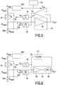
- the electronic circuit - as shown in the circuit diagram of Fig. 5 - contains at least two functional blocks, the bias voltage units V1, V2 and the signal processing unit 20 including a pre-amplifier 25.
- the comparator unit 21 comprises an analog comparator. Its reference level is related to the bias voltage V bias1 over the sensor 10, which in turn is usually derived from a bandgap voltage reference unit VR providing the reference voltage V ref .
- the implementation shown in Fig. 5 is, for instance, preferably used for a MEMS microphone.
- the electronic circuit - as shown in the circuit diagram of Fig. 6 - comprises as third functional block an Analog-to-Digital Converter (ADC) 26.
- ADC Analog-to-Digital Converter
- the pre-amplifier 25 and ADC 26 are interwoven so that only the digital output can be accessed to recognize an overload condition. This is not a limitation because a digital comparator function is preferable over an analog one for reasons of current consumption (which is, for instance, important for mobile applications), ease of design, chip area (cost) and accuracy.
- the common ADC type is a 1-bit Sigma-Delta ADC. Its output signal is a pulse-density modulated bitstream. In case of overload, the stream will consist of a series of subsequent '1's or '0's, depending on the polarity.
- the digital comparator 21' can be a simple counter. Its output V' C becomes active in case a pre-defined number of subsequent '1's occurs.
- a specific advantage of this digital comparator 21' is that the reference level V ref is simply a programmable number.
- FIG. 7 shows timing diagrams of the signal appearing in the analog implementation as depicted in Fig. 5 .
- Fig. 7a shows the distance d between the plates of the MEMS sensor 10.
- a sinusoidal input signal of normal amplitude is applied during interval i1 .
- the distance varies around do with an amplitude smaller than d max .
- a mechanical overload signal occurs which reduces the distance to d 0 -d max .
- an overload condition appears that is detected.
- Fig. 7b shows the output voltage V OUT of the signal processor.
- the overload condition is detected when V OUT exceeds V ref .
- Fig. 7c shows the comparator output signal V C . At detection of the overload condition, the comparator output becomes active.
- Figs. 7d and 7e show the output signals V T1 and V T2 of the pulse generators 23 and 24. It can be seen that the detection of the overload condition causes the output of pulse generators 23 and 24 to become active simultaneously, which closes the switches S1 and S2.
- Fig. 7a As can be seen in Fig. 7a , during interval T1, the membrane returns to its normal position. Here it acts as a purely mechanical spring-mass system. No electrical force is present.
- the pulse generator 23 After interval T1, the pulse generator 23 returns to inactive and the switch S1 is re-opened, as can be seen from Fig. 7d .
- Fig. 7f illustrates, the sensor is rapidly recharged over R bias1 , which is low-ohmic. The voltage reaches e.g. 90% of the final value V bias1 -V bias2 , and the sensor device is ready again for signal conversion.
- the pulse generator 24 After interval T2, the pulse generator 24 returns to inactive and the switch S2 is re-opened. (see Fig. 7e .) As Fig. 7f illustrates, the sensor recharges slowly to its final value over R bias1 and R bias2 , where R bias2 is high-ohmic hence dominant.
- Fig. 8 shows timing diagrams of the input signal V OUT and the output signal V C of the comparator (counter) 21' in the digital implementation as depicted in Fig. 6 .
- Fig. 8a shows the output signal V OUT of the Sigma-Delta ADC 26 (depictive, not on an accurate time schale) in case of a distance signal d as shown in Fig. 7a .
- interval i1 there is normal sensor operation.
- the ADC produces a stream of '1's and '0's with on average equal occurrence.
- interval i2 the sensor moves towards overload.
- the fraction of '1's in the ADC stream rises from 50% to almost 100%.
- Interval i3 represents the overload situation, where the stream only contains '1's.
- the Sigma-Delta ADC 26 is probably not be able to reach a 0% or 100% modulation level, i. e. an output consisting of exclusively '0's or '1's, but just a lower modulation level. e.g. 5% - 95%.
- the output of the comparator (counter) 21' has to become active, when a predefined ratio of '1's and '0's (e.g. 10:1) is exceeded.
- a predefined ratio of '1's and '0's e.g. 10:1
- the ratio between the output of a first counter for the '1's and a second counter for the '0's is evaluated.
- the preset number of subsequent '1's once the output of a single counter becomes active can be lowered compared to the counter for the 100% modulation level so that the discharge procedure is initiated after the same time of overload condition. That means that defining the preset number of subsequent '1's depends on the tolerated time duration of overload condition, the output frequency of the Sigma-Delta ADC 26 and the modulation level which is reached at overload.
- a Sigma-Delta ADC 26 Another limitation for the application of a Sigma-Delta ADC 26 in a practical design is the signal headroom in the Sigma-Delta ADC 26.
- the total gain of pre-amplifier 25 and the Sigma-Delta ADC 26 is dimensioned such that the maximum ADC modulation level coincides with the maximum input signal swing.
- the signal-to-noise ratio of the Sigma-Delta ADC 26 can be a limiting factor in the signal path, meaning that the Sigma-Delta ADC 26 can be the weakest part in the chain with respect to the SNR. So, even signals in the normal operation mode can cause a maximum signal at the output of the Sigma-Delta ADC 26, i.e.
- the Sigma-Delta ADC 26 can start to clip even in the normal operation mode. However, this means there is no headroom left for larger signal excursions which could be used to identify an upcoming overload condition.
- the overload detection has to be performed by an (additional) analog comparator 21 as depicted in Fig. 5 .
- a common way to implement said voltage multiplier is a circuit consisting of switches and capacitors.
- the unloaded output voltage becomes the sum of the individual capacitor voltages.
- a resistive load causes a ripple on the output voltage at the switch frequency of the voltage multiplier.
- the ripple's frequency is well above the audio band (20 kHz), it may still harm the audio performance because aliasing in the Sigma-Delta ADC 26 can fold the ripple frequency back into the audio band.
- an RC filter is used to suppress the ripple at the bias voltage when a load current is drawn from the voltage multiplier.
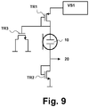
- Fig. 9 shows a practical solution which saves chip area in comparison to a traditional fully-integrated anti-aliasing filter.
- the resistor R bias1 is implemented as a diode, e.g. by a PN-junction or a long-channel MOS transistor TR1 whose gate is connected to the drain and which then acts as a diode.
- the capacitor is implemented as gate of a MOS transistor TR3.
- a typical capacitor value is one order larger than the sensor's capacitance.
- the large decoupling capacitor provides a low impedance level for audio frequencies so effectively the upper sensor node acts as a virtual ground.
- the diode (respectively the transistor TR1 acting as a diode) acts as a low-ohmic resistor and enables fast charging when the bias voltage across the sensor is lower than the voltage multiplier output (directly after power-on or after recovering from an overload).
- the diode has to supply only the (very low) leakage current of the sensor in a steady state.
- the voltage across the diode is low why the diode acts as a very high impedance.
- the RC time constant of the filter becomes sufficiently long to suppress the ripple to a level where aliasing products remain below the noise floor.
- the DC impedance level at the upper node of the sensor is very high.
- the large decoupling capacitor provides a low AC impedance level for audio frequencies so effectively the upper node acts as a virtual ground.
- the resistor R bias2 and voltage source V bias2 are also implemented as a diode or a long-channel MOS transistor TR2 whose gate is connected to the drain and which then acts as a diode. Similarly, it will also conduct a very small leakage current in the steady state. For a PN diode this results in a forward bias of a few hundred mV. For the long-channel MOS transistor TR2 it will also result a Vds of a few hundred mV, which is a convenient DC level for the pre-amplifier 25.
- Fields of application of the present invention are all capacitive MEMS sensors, e.g. MEMS microphones, accelerometers and pressure sensors.
- MEMS sensors e.g. MEMS microphones, accelerometers and pressure sensors.
- the invention can be used as a microphone for a cell phone.
- a magnetic compass, GPS and MEMS accelerometer sensors shall be combined for accurate positioning in portable electronics like cell phones.
- the present invention provides a novel feedback loop for the electronics in capacitive MEMS sensor devices. Its purpose is to let the sensor and its signal-processing electronics recover quickly from an overload caused by a mechanical over-excitation. This invention strongly reduces the duration of the resulting error signal, which is a benefit to the quality of the application. A fast recovery is obtained by an improved bias circuit, no audible side effects are obtained (in case of use as a microphone).
Landscapes
- Physics & Mathematics (AREA)
- General Physics & Mathematics (AREA)
- Engineering & Computer Science (AREA)
- Acoustics & Sound (AREA)
- Signal Processing (AREA)
- Power Engineering (AREA)
- Pressure Sensors (AREA)
- Electrostatic, Electromagnetic, Magneto- Strictive, And Variable-Resistance Transducers (AREA)
- Measuring Fluid Pressure (AREA)
Claims (10)
- Kapazitive MEMS-Sensorvorrichtung zum Abtasten einer mechanischen Größe und die aufweist:- einen kapazitiven MEMS-Messfühler (10) mit zwei Platten (11, 14), die parallel in einem Abstand d0 angeordnet sind, der als Reaktion auf die mechanische Größe (P) variiert, und zum Umwandeln der abgetasteten mechanischen Größe in eine elektrische Größe,- eine erste Vorspannungseinheit (V1) zum Liefern einer ersten Vorspannung (Vbias1) an eine erste Platte des MEMS-Messfühlers, und- eine Signalverarbeitungseinheit (20) zum Verarbeiten der elektrischen Größe in ein Ausgangssignal (VOUT),gekennzeichnet durch:- eine zweite Vorspannungseinheit (V2) zum Liefern einer zweiten Vorspannung (Vbias2) an die zweite Platte des MEMS-Messfühlers,- eine Komparatoreinheit (21) zum Vergleich des Ausgangssignals (VOUT) mit einem Bezugssignal (Vref) zur Erfassung eines Überlastzustands des MEMS-Messfühlers (10) und zur Ausgabe eines Komparatorsignals,- eine Steuereinheit (22) zum Steuern der Entladung des MEMS-Messfühlers (10) im Fall eines vom Komparatorsignal angezeigten Überlastzustands durch Verbinden, im Fall eines Überlastzustands, der ersten Platte mit einem ersten Entladungsanschluss (D) während eines ersten Zeitintervalls (T1) und der zweiten Platte mit einem zweiten Entladungsanschluss (D) während eines zweiten Zeitintervalls (T2);wobei die ersten und zweiten Zeitintervalle (T1, T2) im Wesentlichen die gleiche Startzeit haben und wobei das erste Zeitintervall (T1) kürzer ist als das zweite Zeitintervall (T2).
- Kapazitive MEMS-Sensorvorrichtung nach Anspruch 1,
wobei die erste Vorspannungseinheit (V1) eine erste Spannungsquelle (VS1) und ein erstes Impedanzelement (Rbias1) aufweist, das eine niedrige Impedanz hat und zwischen der ersten Spanungsquelle und der ersten Platte verbunden ist, und
wobei die zweite Vorspannungseinheit (V2) eine zweite Spannungsquelle (VS2) und ein zweites Impedanzelement (Rbias2) aufweist, das eine hohe Impedanz hat und zwischen der zweiten Spannungsquelle und der zweiten Platte verbunden ist. - Kapazitive MEMS-Sensorvorrichtung nach Anspruch 2,
wobei die Verbindung zwischen der zweiten Spannungsquelle (VS2) und dem zweiten Impedanzelement (Rbias2) als der erste und der zweite Entladungsanschluss bereitgestellt wird. - Kapazitive MEMS-Sensorvorrichtung nach Anspruch 2,
wobei die Versorgungsspannung der ersten Spannungsquelle (VS1) größer ist als die Versorgungsspannung der zweiten Spannungsquelle (VS2). - Kapazitive MEMS-Sensorvorrichtung nach Anspruch 1,
wobei die Steuereinheit (22) einen ersten Impulsgenerator (23) mit einer ersten Impulsdauer (T1) entsprechend dem ersten Zeitintervall und einen zweiten Impulsgenerator (24) mit einer zweiten Impulsdauer (T2) entsprechend dem zweiten Zeitintervall aufweist. - Kapazitive MEMS-Sensorvorrichtung nach Anspruch 1,
wobei der erste und der zweite Entladungsanschluss gleich sind, insbesondere einem Vorspannungsversorgungsanschluss der zweiten Vorspannungseinheit (V2) entsprechen. - Kapazitive MEMS-Sensorvorrichtung nach Anspruch 1,
wobei die Steuereinheit (22) einen ersten Schalter (S1) zum Verbinden der ersten Platte mit dem ersten Entladungsanschluss während des ersten Zeitintervalls und einen zweiten Schalter (S2) zum Verbinden der zweiten Platte mit dem zweiten Entladungsanschluss während des zweiten Zeitintervalls aufweist. - Kapazitive MEMS-Sensorvorrichtung nach Anspruch 1, wobei die Signalverarbeitungseinheit (20) einen analogen Signalverstärker (25) aufweist,
wobei die Komparatoreinheit (21) einen analogen Komparator aufweist, und
wobei die erste Vorspannung (Vbias1) von der Bezugsspannung (Vref) abgeleitet wird. - Kapazitive MEMS-Sensorvorrichtung nach Anspruch 1,
wobei die Signalverarbeitungseinheit (20) einen analogen Signalverstärker (25) und einen Analog-Digital-Wandler (26) zum Umwandeln des Verstärkerausgangssignals in ein digitales Ausgangssignals (VOUT) aufweist, und wobei die Komparatoreinheit (21') einen digitalen Komparator aufweist, insbesondere einen Zähler zur Erfassung einer vorbestimmten Anzahl von nachfolgenden Bits, die einen vorbestimmten Bitwert haben. - Verfahren für den Betrieb einer kapazitiven MEMS-Sensorvorrichtung zum Abtasten einer mechanischen Größe mit einem kapazitiven MEMS-Messfühler (10) mit zwei Platten (11, 14), die parallel in einem Abstand d0 angeordnet sind, der sich als Reaktion auf die mechanische Größe (P) ändert, und um die abgetastete mechanische Größe in eine elektrische Größe umzuwandeln, das die folgenden Schritte aufweist:- Liefern einer ersten Vorspannung (Vbias1) an eine erste Platte des MEMS-Messfühlers,- Liefern einer zweiten Vorspannung (Vbias2) an die zweite Platte des MEMS-Messfühlers,- Verarbeiten der elektrischen Größe in ein Ausgangssignal (VOUT),- Vergleichen des Ausgangssignals (VOUT) mit einem Bezugssignal (Vref) zur Erfassung eines Überlastzustands des MEMS-Messfühlers (10) und zur Ausgabe eines Komparatorsignals,- Steuern der Entladung des MEMS-Messfühlers (10) im Fall eines vom Komparatorsignal angezeigten Überlastzustands durch Verbinden, im Fall eines Überlastzustands, der ersten Platte mit einem ersten Entladungsanschluss während eines ersten Zeitintervalls (T1) und der zweiten Platte mit einem zweiten Entladungsanschluss während eines zweiten Zeitintervalls (T2),wobei das erste und das zweite Zeitintervall (T1, T2) im Wesentlichen die gleiche Startzeit haben und wobei das erste Zeitintervall (T1) kürzer ist als das zweite Zeitintervall (T).
Priority Applications (1)
| Application Number | Priority Date | Filing Date | Title |
|---|---|---|---|
| EP07735891.9A EP2021739B1 (de) | 2006-05-17 | 2007-05-14 | Kapazitive mems-sensoranordnung |
Applications Claiming Priority (3)
| Application Number | Priority Date | Filing Date | Title |
|---|---|---|---|
| EP06114074 | 2006-05-17 | ||
| PCT/IB2007/051820 WO2007132422A1 (en) | 2006-05-17 | 2007-05-14 | Capacitive mems sensor device |
| EP07735891.9A EP2021739B1 (de) | 2006-05-17 | 2007-05-14 | Kapazitive mems-sensoranordnung |
Publications (2)
| Publication Number | Publication Date |
|---|---|
| EP2021739A1 EP2021739A1 (de) | 2009-02-11 |
| EP2021739B1 true EP2021739B1 (de) | 2017-10-11 |
Family
ID=38529693
Family Applications (1)
| Application Number | Title | Priority Date | Filing Date |
|---|---|---|---|
| EP07735891.9A Active EP2021739B1 (de) | 2006-05-17 | 2007-05-14 | Kapazitive mems-sensoranordnung |
Country Status (5)
| Country | Link |
|---|---|
| US (1) | US8134375B2 (de) |
| EP (1) | EP2021739B1 (de) |
| JP (1) | JP2009537817A (de) |
| CN (1) | CN101443633B (de) |
| WO (1) | WO2007132422A1 (de) |
Cited By (1)
| Publication number | Priority date | Publication date | Assignee | Title |
|---|---|---|---|---|
| TWI847421B (zh) * | 2022-12-12 | 2024-07-01 | 財團法人工業技術研究院 | 電訊號還原系統及電訊號還原方法 |
Families Citing this family (41)
| Publication number | Priority date | Publication date | Assignee | Title |
|---|---|---|---|---|
| US8401208B2 (en) * | 2007-11-14 | 2013-03-19 | Infineon Technologies Ag | Anti-shock methods for processing capacitive sensor signals |
| US8288971B2 (en) * | 2008-01-11 | 2012-10-16 | Broadcom Corporation | Integrated and programmable microphone bias generation |
| GB2459862B (en) * | 2008-05-07 | 2010-06-30 | Wolfson Microelectronics Plc | Capacitive transducer circuit and method |
| GB2459864A (en) * | 2008-05-07 | 2009-11-11 | Wolfson Microelectronics Plc | Filtered bias voltage for a MEMS capacitive transducer circuit |
| WO2010103452A1 (en) | 2009-03-11 | 2010-09-16 | Nxp B.V. | Low-frequency filter comprising maxwell-wagner stack |
| IT1396063B1 (it) * | 2009-03-31 | 2012-11-09 | St Microelectronics Rousset | Circuito di polarizzazione per un trasduttore acustico microelettromeccanico e relativo metodo di polarizzazione |
| EP2367366B1 (de) * | 2010-03-17 | 2012-11-14 | Nxp B.V. | Steuerung eines Mikrofons |
| US8513948B2 (en) * | 2010-11-22 | 2013-08-20 | International Business Machines Corporation | Microelectromechanical structure (MEMS) monitoring |
| US9525925B2 (en) | 2011-02-25 | 2016-12-20 | Infineon Technologies Ag | Sensor with movable part and biasing |
| EP2681928A1 (de) * | 2011-03-04 | 2014-01-08 | Sony Mobile Communications AB | Verfahren zur ansteuerung einer kondensatormikrofons |
| US8405449B2 (en) | 2011-03-04 | 2013-03-26 | Akustica, Inc. | Resettable high-voltage capable high impedance biasing network for capacitive sensors |
| CN103733304B (zh) * | 2011-06-29 | 2016-08-17 | 因文森斯公司 | 其中一部分暴露在环境下并且带有竖直集成电子器件的气密封mems设备 |
| US9236837B2 (en) * | 2011-08-25 | 2016-01-12 | Infineon Technologies Ag | System and method for low distortion capacitive signal source amplifier |
| DE102011113431B4 (de) | 2011-09-14 | 2017-01-26 | Austriamicrosystems Ag | Mikrofonverstärker |
| US8630429B2 (en) | 2011-12-16 | 2014-01-14 | Robert Bosch Gmbh | Preventing electrostatic pull-in in capacitive devices |
| DE112012006158B4 (de) | 2012-03-30 | 2019-03-21 | Tdk Corporation | Mikrofon mit automatischer Vorspannungsregelung |
| DE102012020271A1 (de) * | 2012-10-17 | 2014-04-17 | Wolfgang Klippel | Anordnung und Verfahren zur Steuerung von Wandlern |
| KR20150087410A (ko) * | 2012-12-19 | 2015-07-29 | 노우레스 일렉트로닉스, 엘엘시 | 고전압 i/o 정-전기 방전 보호를 위한 장치 및 방법 |
| US9258660B2 (en) * | 2013-03-14 | 2016-02-09 | Robert Bosch Gmbh | Reset circuit for MEMS capacitive microphones |
| US9574907B2 (en) | 2013-03-15 | 2017-02-21 | Semtech Corporation | Semiconductor device and method of direct measurement and acquisition of MEMS employing sigma-delta loop |
| US9419562B1 (en) * | 2013-04-09 | 2016-08-16 | Cirrus Logic, Inc. | Systems and methods for minimizing noise in an amplifier |
| US9517930B2 (en) * | 2013-06-28 | 2016-12-13 | Hanking Electronics, Ltd. | Recovery system and methods for MEMS devices |
| WO2016036422A1 (en) * | 2014-09-05 | 2016-03-10 | Cavendish Kinetics, Inc | Internally generated dft stepped hysteresis sweep for electrostatic mems |
| US9319779B2 (en) | 2013-10-22 | 2016-04-19 | Infineon Technologies Ag | System and method for transducer biasing and shock protection |
| TWI538096B (zh) | 2013-12-31 | 2016-06-11 | 財團法人工業技術研究院 | 具pn界面的微機電裝置 |
| US10142729B2 (en) | 2014-05-20 | 2018-11-27 | Tdk Corporation | Microphone and method of operating a microphone |
| US9513184B2 (en) * | 2014-06-11 | 2016-12-06 | Ams International Ag | MEMS device calibration |
| US9462395B2 (en) * | 2014-07-22 | 2016-10-04 | Stmicroelectronics S.R.L. | Biasing circuit for a MEMS acoustic transducer with reduced start-up time |
| EP3192278B1 (de) * | 2014-09-10 | 2019-07-03 | Robert Bosch GmbH | Verfahren zur erkennung von defekten eines mems-mikrofon-hochimpedanzschaltkreises |
| US9942677B2 (en) * | 2014-09-15 | 2018-04-10 | Infineon Technologies Ag | System and method for a transducer |
| CN105491492B (zh) * | 2014-09-23 | 2019-04-26 | 山东共达电声股份有限公司 | 一种自校准硅麦克风装置和校准方法 |
| FR3030739B1 (fr) | 2014-12-18 | 2019-05-03 | Commissariat A L'energie Atomique Et Aux Energies Alternatives | Capteur de pression dynamique a fonctionnement ameliore |
| US10200036B1 (en) | 2015-06-30 | 2019-02-05 | The Charles Stark Draper Laboratory, Inc. | Radiation-hard precision voltage reference |
| CN106714057A (zh) * | 2015-11-13 | 2017-05-24 | 钰太芯微电子科技(上海)有限公司 | 动态追踪的mems麦克风及动态追踪方法 |
| CN108702565B (zh) * | 2015-12-21 | 2021-03-12 | Tdk株式会社 | Mems电容性传感器 |
| US10212500B2 (en) * | 2017-01-27 | 2019-02-19 | Apple Inc. | Digital transducer circuit |
| WO2019021509A1 (ja) * | 2017-07-25 | 2019-01-31 | 三菱電機株式会社 | 家電機器 |
| US12253391B2 (en) | 2018-05-24 | 2025-03-18 | The Research Foundation For The State University Of New York | Multielectrode capacitive sensor without pull-in risk |
| US11235970B1 (en) * | 2019-05-30 | 2022-02-01 | Apple Inc. | Overload recovery optimization in microelectromechanical system application specific integrated circuit |
| CN114040301B (zh) * | 2021-11-15 | 2024-02-27 | 歌尔微电子股份有限公司 | 麦克风快速启动电路、麦克风芯片及麦克风 |
| CN114674348B (zh) * | 2022-04-19 | 2024-04-12 | 杭州电子科技大学 | 基于摩擦纳米发电机的幅度和频率双参数传感解耦系统 |
Family Cites Families (4)
| Publication number | Priority date | Publication date | Assignee | Title |
|---|---|---|---|---|
| US6285769B1 (en) * | 1997-04-10 | 2001-09-04 | Borealis Technical Limited | Force balance microphone |
| US6088463A (en) * | 1998-10-30 | 2000-07-11 | Microtronic A/S | Solid state silicon-based condenser microphone |
| EP1106981A3 (de) | 1999-12-09 | 2002-07-24 | Texas Instruments Incorporated | Kapazitiver Wandler |
| EP1599067B1 (de) * | 2004-05-21 | 2013-05-01 | Epcos Pte Ltd | Detektion und Kontrolle des Membrankollaps in einem Kondensatormikrofon |
-
2007
- 2007-05-14 CN CN2007800176524A patent/CN101443633B/zh not_active Expired - Fee Related
- 2007-05-14 WO PCT/IB2007/051820 patent/WO2007132422A1/en not_active Ceased
- 2007-05-14 EP EP07735891.9A patent/EP2021739B1/de active Active
- 2007-05-14 JP JP2009510598A patent/JP2009537817A/ja not_active Withdrawn
- 2007-05-14 US US12/301,163 patent/US8134375B2/en not_active Expired - Fee Related
Non-Patent Citations (1)
| Title |
|---|
| None * |
Cited By (2)
| Publication number | Priority date | Publication date | Assignee | Title |
|---|---|---|---|---|
| TWI847421B (zh) * | 2022-12-12 | 2024-07-01 | 財團法人工業技術研究院 | 電訊號還原系統及電訊號還原方法 |
| US12455200B2 (en) | 2022-12-12 | 2025-10-28 | Industrial Technology Research Institute | Electric signal reconstruction system and method |
Also Published As
| Publication number | Publication date |
|---|---|
| WO2007132422A1 (en) | 2007-11-22 |
| CN101443633B (zh) | 2011-03-16 |
| CN101443633A (zh) | 2009-05-27 |
| EP2021739A1 (de) | 2009-02-11 |
| JP2009537817A (ja) | 2009-10-29 |
| US8134375B2 (en) | 2012-03-13 |
| US20100013501A1 (en) | 2010-01-21 |
Similar Documents
| Publication | Publication Date | Title |
|---|---|---|
| EP2021739B1 (de) | Kapazitive mems-sensoranordnung | |
| US7548626B2 (en) | Detection and control of diaphragm collapse in condenser microphones | |
| US20120043974A1 (en) | Circuit and method for monitoring a capacitive signal source | |
| US8675895B2 (en) | Microphone assembly with integrated self-test circuitry | |
| US9722563B2 (en) | System and method for high input capacitive signal amplifier | |
| CN103226368B (zh) | 快速加电偏置电压电路 | |
| US20200252729A1 (en) | Sensor arrangement and method for providing a sensor signal | |
| US20170272879A1 (en) | Glitch Detection and Method for Detecting a Glitch | |
| KR20130023132A (ko) | 저왜곡 용량성 신호 소스 증폭기를 위한 시스템 및 방법 | |
| EP1988366A1 (de) | Schaltung mit Ableseschnittstelle für einen kapazitiven mikroelektromechanischen Sensor und entsprechender Sensor | |
| US10965262B2 (en) | Interface electronic circuit for a microelectromechanical acoustic transducer and corresponding method | |
| US10080082B2 (en) | Microphone system having high acoustical overload point | |
| US10531213B2 (en) | MEMS transducer system | |
| CN104581587B (zh) | 用于换能器偏置和震动保护的系统和方法 | |
| KR20170124092A (ko) | 고저항 저항기를 위한 시스템 및 방법 | |
| US10972848B2 (en) | MEMS transducer system and associated methods |
Legal Events
| Date | Code | Title | Description |
|---|---|---|---|
| PUAI | Public reference made under article 153(3) epc to a published international application that has entered the european phase |
Free format text: ORIGINAL CODE: 0009012 |
|
| 17P | Request for examination filed |
Effective date: 20081217 |
|
| AK | Designated contracting states |
Kind code of ref document: A1 Designated state(s): AT BE BG CH CY CZ DE DK EE ES FI FR GB GR HU IE IS IT LI LT LU LV MC MT NL PL PT RO SE SI SK TR |
|
| AX | Request for extension of the european patent |
Extension state: AL BA HR MK RS |
|
| 17Q | First examination report despatched |
Effective date: 20090311 |
|
| RAP1 | Party data changed (applicant data changed or rights of an application transferred) |
Owner name: III HOLDINGS 6, LLC |
|
| GRAP | Despatch of communication of intention to grant a patent |
Free format text: ORIGINAL CODE: EPIDOSNIGR1 |
|
| INTG | Intention to grant announced |
Effective date: 20170420 |
|
| GRAS | Grant fee paid |
Free format text: ORIGINAL CODE: EPIDOSNIGR3 |
|
| GRAA | (expected) grant |
Free format text: ORIGINAL CODE: 0009210 |
|
| AK | Designated contracting states |
Kind code of ref document: B1 Designated state(s): AT BE BG CH CY CZ DE DK EE ES FI FR GB GR HU IE IS IT LI LT LU LV MC MT NL PL PT RO SE SI SK TR |
|
| AX | Request for extension of the european patent |
Extension state: AL BA HR MK RS |
|
| REG | Reference to a national code |
Ref country code: GB Ref legal event code: FG4D |
|
| REG | Reference to a national code |
Ref country code: CH Ref legal event code: EP |
|
| REG | Reference to a national code |
Ref country code: IE Ref legal event code: FG4D |
|
| REG | Reference to a national code |
Ref country code: AT Ref legal event code: REF Ref document number: 936453 Country of ref document: AT Kind code of ref document: T Effective date: 20171115 |
|
| REG | Reference to a national code |
Ref country code: DE Ref legal event code: R096 Ref document number: 602007052651 Country of ref document: DE |
|
| REG | Reference to a national code |
Ref country code: NL Ref legal event code: MP Effective date: 20171011 |
|
| REG | Reference to a national code |
Ref country code: LT Ref legal event code: MG4D |
|
| REG | Reference to a national code |
Ref country code: AT Ref legal event code: MK05 Ref document number: 936453 Country of ref document: AT Kind code of ref document: T Effective date: 20171011 |
|
| PG25 | Lapsed in a contracting state [announced via postgrant information from national office to epo] |
Ref country code: NL Free format text: LAPSE BECAUSE OF FAILURE TO SUBMIT A TRANSLATION OF THE DESCRIPTION OR TO PAY THE FEE WITHIN THE PRESCRIBED TIME-LIMIT Effective date: 20171011 |
|
| REG | Reference to a national code |
Ref country code: FR Ref legal event code: PLFP Year of fee payment: 12 |
|
| PG25 | Lapsed in a contracting state [announced via postgrant information from national office to epo] |
Ref country code: SE Free format text: LAPSE BECAUSE OF FAILURE TO SUBMIT A TRANSLATION OF THE DESCRIPTION OR TO PAY THE FEE WITHIN THE PRESCRIBED TIME-LIMIT Effective date: 20171011 Ref country code: LT Free format text: LAPSE BECAUSE OF FAILURE TO SUBMIT A TRANSLATION OF THE DESCRIPTION OR TO PAY THE FEE WITHIN THE PRESCRIBED TIME-LIMIT Effective date: 20171011 Ref country code: ES Free format text: LAPSE BECAUSE OF FAILURE TO SUBMIT A TRANSLATION OF THE DESCRIPTION OR TO PAY THE FEE WITHIN THE PRESCRIBED TIME-LIMIT Effective date: 20171011 Ref country code: FI Free format text: LAPSE BECAUSE OF FAILURE TO SUBMIT A TRANSLATION OF THE DESCRIPTION OR TO PAY THE FEE WITHIN THE PRESCRIBED TIME-LIMIT Effective date: 20171011 |
|
| PG25 | Lapsed in a contracting state [announced via postgrant information from national office to epo] |
Ref country code: GR Free format text: LAPSE BECAUSE OF FAILURE TO SUBMIT A TRANSLATION OF THE DESCRIPTION OR TO PAY THE FEE WITHIN THE PRESCRIBED TIME-LIMIT Effective date: 20180112 Ref country code: BG Free format text: LAPSE BECAUSE OF FAILURE TO SUBMIT A TRANSLATION OF THE DESCRIPTION OR TO PAY THE FEE WITHIN THE PRESCRIBED TIME-LIMIT Effective date: 20180111 Ref country code: LV Free format text: LAPSE BECAUSE OF FAILURE TO SUBMIT A TRANSLATION OF THE DESCRIPTION OR TO PAY THE FEE WITHIN THE PRESCRIBED TIME-LIMIT Effective date: 20171011 Ref country code: AT Free format text: LAPSE BECAUSE OF FAILURE TO SUBMIT A TRANSLATION OF THE DESCRIPTION OR TO PAY THE FEE WITHIN THE PRESCRIBED TIME-LIMIT Effective date: 20171011 Ref country code: IS Free format text: LAPSE BECAUSE OF FAILURE TO SUBMIT A TRANSLATION OF THE DESCRIPTION OR TO PAY THE FEE WITHIN THE PRESCRIBED TIME-LIMIT Effective date: 20180211 |
|
| REG | Reference to a national code |
Ref country code: DE Ref legal event code: R097 Ref document number: 602007052651 Country of ref document: DE |
|
| PG25 | Lapsed in a contracting state [announced via postgrant information from national office to epo] |
Ref country code: CZ Free format text: LAPSE BECAUSE OF FAILURE TO SUBMIT A TRANSLATION OF THE DESCRIPTION OR TO PAY THE FEE WITHIN THE PRESCRIBED TIME-LIMIT Effective date: 20171011 Ref country code: EE Free format text: LAPSE BECAUSE OF FAILURE TO SUBMIT A TRANSLATION OF THE DESCRIPTION OR TO PAY THE FEE WITHIN THE PRESCRIBED TIME-LIMIT Effective date: 20171011 Ref country code: DK Free format text: LAPSE BECAUSE OF FAILURE TO SUBMIT A TRANSLATION OF THE DESCRIPTION OR TO PAY THE FEE WITHIN THE PRESCRIBED TIME-LIMIT Effective date: 20171011 Ref country code: SK Free format text: LAPSE BECAUSE OF FAILURE TO SUBMIT A TRANSLATION OF THE DESCRIPTION OR TO PAY THE FEE WITHIN THE PRESCRIBED TIME-LIMIT Effective date: 20171011 |
|
| PLBE | No opposition filed within time limit |
Free format text: ORIGINAL CODE: 0009261 |
|
| STAA | Information on the status of an ep patent application or granted ep patent |
Free format text: STATUS: NO OPPOSITION FILED WITHIN TIME LIMIT |
|
| PG25 | Lapsed in a contracting state [announced via postgrant information from national office to epo] |
Ref country code: IT Free format text: LAPSE BECAUSE OF FAILURE TO SUBMIT A TRANSLATION OF THE DESCRIPTION OR TO PAY THE FEE WITHIN THE PRESCRIBED TIME-LIMIT Effective date: 20171011 Ref country code: RO Free format text: LAPSE BECAUSE OF FAILURE TO SUBMIT A TRANSLATION OF THE DESCRIPTION OR TO PAY THE FEE WITHIN THE PRESCRIBED TIME-LIMIT Effective date: 20171011 Ref country code: PL Free format text: LAPSE BECAUSE OF FAILURE TO SUBMIT A TRANSLATION OF THE DESCRIPTION OR TO PAY THE FEE WITHIN THE PRESCRIBED TIME-LIMIT Effective date: 20171011 |
|
| 26N | No opposition filed |
Effective date: 20180712 |
|
| PG25 | Lapsed in a contracting state [announced via postgrant information from national office to epo] |
Ref country code: SI Free format text: LAPSE BECAUSE OF FAILURE TO SUBMIT A TRANSLATION OF THE DESCRIPTION OR TO PAY THE FEE WITHIN THE PRESCRIBED TIME-LIMIT Effective date: 20171011 |
|
| REG | Reference to a national code |
Ref country code: CH Ref legal event code: PL |
|
| REG | Reference to a national code |
Ref country code: BE Ref legal event code: MM Effective date: 20180531 |
|
| PG25 | Lapsed in a contracting state [announced via postgrant information from national office to epo] |
Ref country code: MC Free format text: LAPSE BECAUSE OF FAILURE TO SUBMIT A TRANSLATION OF THE DESCRIPTION OR TO PAY THE FEE WITHIN THE PRESCRIBED TIME-LIMIT Effective date: 20171011 |
|
| REG | Reference to a national code |
Ref country code: IE Ref legal event code: MM4A |
|
| PG25 | Lapsed in a contracting state [announced via postgrant information from national office to epo] |
Ref country code: LI Free format text: LAPSE BECAUSE OF NON-PAYMENT OF DUE FEES Effective date: 20180531 Ref country code: CH Free format text: LAPSE BECAUSE OF NON-PAYMENT OF DUE FEES Effective date: 20180531 |
|
| PG25 | Lapsed in a contracting state [announced via postgrant information from national office to epo] |
Ref country code: LU Free format text: LAPSE BECAUSE OF NON-PAYMENT OF DUE FEES Effective date: 20180514 |
|
| PG25 | Lapsed in a contracting state [announced via postgrant information from national office to epo] |
Ref country code: IE Free format text: LAPSE BECAUSE OF NON-PAYMENT OF DUE FEES Effective date: 20180514 |
|
| PG25 | Lapsed in a contracting state [announced via postgrant information from national office to epo] |
Ref country code: BE Free format text: LAPSE BECAUSE OF NON-PAYMENT OF DUE FEES Effective date: 20180531 |
|
| PG25 | Lapsed in a contracting state [announced via postgrant information from national office to epo] |
Ref country code: MT Free format text: LAPSE BECAUSE OF NON-PAYMENT OF DUE FEES Effective date: 20180514 |
|
| PG25 | Lapsed in a contracting state [announced via postgrant information from national office to epo] |
Ref country code: TR Free format text: LAPSE BECAUSE OF FAILURE TO SUBMIT A TRANSLATION OF THE DESCRIPTION OR TO PAY THE FEE WITHIN THE PRESCRIBED TIME-LIMIT Effective date: 20171011 |
|
| PG25 | Lapsed in a contracting state [announced via postgrant information from national office to epo] |
Ref country code: PT Free format text: LAPSE BECAUSE OF FAILURE TO SUBMIT A TRANSLATION OF THE DESCRIPTION OR TO PAY THE FEE WITHIN THE PRESCRIBED TIME-LIMIT Effective date: 20171011 Ref country code: HU Free format text: LAPSE BECAUSE OF FAILURE TO SUBMIT A TRANSLATION OF THE DESCRIPTION OR TO PAY THE FEE WITHIN THE PRESCRIBED TIME-LIMIT; INVALID AB INITIO Effective date: 20070514 |
|
| PG25 | Lapsed in a contracting state [announced via postgrant information from national office to epo] |
Ref country code: CY Free format text: LAPSE BECAUSE OF FAILURE TO SUBMIT A TRANSLATION OF THE DESCRIPTION OR TO PAY THE FEE WITHIN THE PRESCRIBED TIME-LIMIT Effective date: 20171011 |
|
| PGFP | Annual fee paid to national office [announced via postgrant information from national office to epo] |
Ref country code: GB Payment date: 20220524 Year of fee payment: 16 Ref country code: FR Payment date: 20220526 Year of fee payment: 16 Ref country code: DE Payment date: 20220527 Year of fee payment: 16 |
|
| REG | Reference to a national code |
Ref country code: DE Ref legal event code: R119 Ref document number: 602007052651 Country of ref document: DE |
|
| GBPC | Gb: european patent ceased through non-payment of renewal fee |
Effective date: 20230514 |
|
| PG25 | Lapsed in a contracting state [announced via postgrant information from national office to epo] |
Ref country code: DE Free format text: LAPSE BECAUSE OF NON-PAYMENT OF DUE FEES Effective date: 20231201 Ref country code: GB Free format text: LAPSE BECAUSE OF NON-PAYMENT OF DUE FEES Effective date: 20230514 |
|
| PG25 | Lapsed in a contracting state [announced via postgrant information from national office to epo] |
Ref country code: FR Free format text: LAPSE BECAUSE OF NON-PAYMENT OF DUE FEES Effective date: 20230531 |