EP2020339A1 - Activation device for the safety device in a motor vehicle - Google Patents
Activation device for the safety device in a motor vehicle Download PDFInfo
- Publication number
- EP2020339A1 EP2020339A1 EP07014972A EP07014972A EP2020339A1 EP 2020339 A1 EP2020339 A1 EP 2020339A1 EP 07014972 A EP07014972 A EP 07014972A EP 07014972 A EP07014972 A EP 07014972A EP 2020339 A1 EP2020339 A1 EP 2020339A1
- Authority
- EP
- European Patent Office
- Prior art keywords
- cmos chip
- tripping device
- tripping
- sensor
- measuring
- Prior art date
- Legal status (The legal status is an assumption and is not a legal conclusion. Google has not performed a legal analysis and makes no representation as to the accuracy of the status listed.)
- Granted
Links
Images


Classifications
-
- B—PERFORMING OPERATIONS; TRANSPORTING
- B60—VEHICLES IN GENERAL
- B60R—VEHICLES, VEHICLE FITTINGS, OR VEHICLE PARTS, NOT OTHERWISE PROVIDED FOR
- B60R21/00—Arrangements or fittings on vehicles for protecting or preventing injuries to occupants or pedestrians in case of accidents or other traffic risks
- B60R21/01—Electrical circuits for triggering passive safety arrangements, e.g. airbags, safety belt tighteners, in case of vehicle accidents or impending vehicle accidents
- B60R21/013—Electrical circuits for triggering passive safety arrangements, e.g. airbags, safety belt tighteners, in case of vehicle accidents or impending vehicle accidents including means for detecting collisions, impending collisions or roll-over
- B60R21/0136—Electrical circuits for triggering passive safety arrangements, e.g. airbags, safety belt tighteners, in case of vehicle accidents or impending vehicle accidents including means for detecting collisions, impending collisions or roll-over responsive to actual contact with an obstacle, e.g. to vehicle deformation, bumper displacement or bumper velocity relative to the vehicle
-
- G—PHYSICS
- G01—MEASURING; TESTING
- G01D—MEASURING NOT SPECIALLY ADAPTED FOR A SPECIFIC VARIABLE; ARRANGEMENTS FOR MEASURING TWO OR MORE VARIABLES NOT COVERED IN A SINGLE OTHER SUBCLASS; TARIFF METERING APPARATUS; MEASURING OR TESTING NOT OTHERWISE PROVIDED FOR
- G01D11/00—Component parts of measuring arrangements not specially adapted for a specific variable
- G01D11/24—Housings ; Casings for instruments
- G01D11/245—Housings for sensors
-
- G—PHYSICS
- G01—MEASURING; TESTING
- G01D—MEASURING NOT SPECIALLY ADAPTED FOR A SPECIFIC VARIABLE; ARRANGEMENTS FOR MEASURING TWO OR MORE VARIABLES NOT COVERED IN A SINGLE OTHER SUBCLASS; TARIFF METERING APPARATUS; MEASURING OR TESTING NOT OTHERWISE PROVIDED FOR
- G01D11/00—Component parts of measuring arrangements not specially adapted for a specific variable
- G01D11/30—Supports specially adapted for an instrument; Supports specially adapted for a set of instruments
-
- B—PERFORMING OPERATIONS; TRANSPORTING
- B60—VEHICLES IN GENERAL
- B60R—VEHICLES, VEHICLE FITTINGS, OR VEHICLE PARTS, NOT OTHERWISE PROVIDED FOR
- B60R21/00—Arrangements or fittings on vehicles for protecting or preventing injuries to occupants or pedestrians in case of accidents or other traffic risks
- B60R21/01—Electrical circuits for triggering passive safety arrangements, e.g. airbags, safety belt tighteners, in case of vehicle accidents or impending vehicle accidents
- B60R2021/01006—Mounting of electrical components in vehicles
-
- H—ELECTRICITY
- H01—ELECTRIC ELEMENTS
- H01L—SEMICONDUCTOR DEVICES NOT COVERED BY CLASS H10
- H01L2224/00—Indexing scheme for arrangements for connecting or disconnecting semiconductor or solid-state bodies and methods related thereto as covered by H01L24/00
- H01L2224/01—Means for bonding being attached to, or being formed on, the surface to be connected, e.g. chip-to-package, die-attach, "first-level" interconnects; Manufacturing methods related thereto
- H01L2224/42—Wire connectors; Manufacturing methods related thereto
- H01L2224/47—Structure, shape, material or disposition of the wire connectors after the connecting process
- H01L2224/48—Structure, shape, material or disposition of the wire connectors after the connecting process of an individual wire connector
- H01L2224/4805—Shape
- H01L2224/4809—Loop shape
- H01L2224/48091—Arched
-
- H—ELECTRICITY
- H01—ELECTRIC ELEMENTS
- H01L—SEMICONDUCTOR DEVICES NOT COVERED BY CLASS H10
- H01L2224/00—Indexing scheme for arrangements for connecting or disconnecting semiconductor or solid-state bodies and methods related thereto as covered by H01L24/00
- H01L2224/01—Means for bonding being attached to, or being formed on, the surface to be connected, e.g. chip-to-package, die-attach, "first-level" interconnects; Manufacturing methods related thereto
- H01L2224/42—Wire connectors; Manufacturing methods related thereto
- H01L2224/47—Structure, shape, material or disposition of the wire connectors after the connecting process
- H01L2224/49—Structure, shape, material or disposition of the wire connectors after the connecting process of a plurality of wire connectors
- H01L2224/491—Disposition
- H01L2224/4912—Layout
- H01L2224/49175—Parallel arrangements
-
- H—ELECTRICITY
- H01—ELECTRIC ELEMENTS
- H01L—SEMICONDUCTOR DEVICES NOT COVERED BY CLASS H10
- H01L2224/00—Indexing scheme for arrangements for connecting or disconnecting semiconductor or solid-state bodies and methods related thereto as covered by H01L24/00
- H01L2224/73—Means for bonding being of different types provided for in two or more of groups H01L2224/10, H01L2224/18, H01L2224/26, H01L2224/34, H01L2224/42, H01L2224/50, H01L2224/63, H01L2224/71
- H01L2224/732—Location after the connecting process
- H01L2224/73251—Location after the connecting process on different surfaces
- H01L2224/73265—Layer and wire connectors
Definitions
- the invention relates to a triggering device for a safety device in a motor vehicle, in particular for an airbag, having an electrical component having at least one force sensor, which is fastened to the body of the motor vehicle such that a measurement signal output of the force sensor is dependent on the deformation of the body measurement signal can be applied, and with an evaluation device connected to the measurement signal output for processing the measurement signal.
- Such a triggering device is off DE 43 25 414 C2 known.
- force sensors it has foil pressure sensors whose electrical resistance is inversely proportional to the impressed force.
- the Follendrucksensoren are connected to an evaluation device that generates a trigger signal for the safety device in response to the measurement signals.
- the Follendrucksensoren are arranged on a side door of the motor vehicle between the outer skin of the vehicle body and a protective strip on the protective strip facing away from the back of the outer skin is at a distance from this a reinforcing profile arranged.
- the force sensor has at least one piezoelectric element which is monolithically integrated into a CMOS chip together with the evaluation device.
- a piezo element is understood in particular to be a piezoresitive element.
- the piezoelectric element can also be designed such that it is under the action of a force an electrical voltage generated.
- a CMOS chip is also understood to mean a Bi-CMOS chip in which at least one bipolar component is integrated in addition to at least one CMOS component.
- a CMOS chip is also understood to be a so-called BCDMOS into which at least one DMOS transistor is integrated.
- the at least one force sensor and the evaluation device can then be manufactured inexpensively in large quantities as a CMOS chip using a standard CMOS process, wherein the electrical connection lines between the force sensor and the evaluation device can also be integrated into the CMOS chip.
- the evaluation device preferably comprises at least one filter for the measurement signal of the piezoelectric element.
- the filtered measurement signal which preferably has a smaller data volume than the unfiltered measurement signal, can then be transmitted to a further semiconductor chip in order there to depend on the filtered measurement signal and possibly the filtered measurement signal of at least one further, a piezoelectric element and an evaluation CMOS chip to generate a trigger signal for the safety device.
- the CMOS chip on a plurality of piezoelectric elements which are preferably connected to a bridge circuit, in particular a Wheatstone bridge with each other.
- a bridge circuit in particular a Wheatstone bridge with each other.
- changes in the measurement signal due to temperature fluctuations and / or tolerances in the piezoelectric elements can be largely avoided.
- a temperature sensor having a compensation circuit is integrated to compensate for any remaining dependence of the measurement signal from the temperature in the CMOS chip.
- the bridge circuit can also be simulated by software, wherein the measurement signals of a plurality of piezo elements are detected separately from each other and linked together using a microcomputer.
- the evaluation device has a non-volatile data memory in which at least one tripping characteristic value is stored, wherein the evaluation device has a comparison device for comparing the at least one tripping characteristic value with the measurement signal, and wherein the evaluation device is configured such that a tripping signal in Depending on the result of this comparison can be generated.
- a data store Preferably, an E 2 -Prom is provided.
- the CMOS chip can then be adapted in a simple manner to different motor vehicles and / or different installation situations in a motor vehicle by programming one or more corresponding characteristics into the data memory, which adapt the CMOS chip to the respective desired triggering characteristic. Thus, the same CMOS chip can be used for different applications.
- the CMOS chip has a plurality of piezoelectric elements connected to the evaluation device, with which force measuring signals for at least two main measuring directions arranged transversely to one another can be measured, and if the evaluation device is configured such that the triggering signal depends on the magnitude, the rate of change and / or the direction of a resulting measurement signal formed from the measurement signals can be generated.
- the evaluation device is configured such that the triggering signal depends on the magnitude, the rate of change and / or the direction of a resulting measurement signal formed from the measurement signals can be generated.
- the triggering device has at least two piezoelectric elements which are arranged at an angle of approximately 45 ° to each other, wherein at least one of these piezoelectric elements with its main measuring direction preferably parallel to the orientation of the crystals in the CMOS chip and / or to an edge region and / or edge of the CMOS chips is arranged.
- the piezoelectric element arranged with its measuring direction in one direction the surface voltage of the CMOS chip is mainly measured, while with the piezoelectric element arranged with its measuring direction in the other direction, mainly the shearing voltage in the CMOS chip or the torque acting on the CMOS chip is measured.
- the piezoelectric elements are preferably arranged such that the shear stress and the surface tension in each case in three transversely and preferably orthogonally extending axes (a, b, c or x, y, z) can be measured.
- the CMOS chip via at least one preferably approximately parallel to its main extension plane extending adhesive layer and non-positively connected to a first surface region of the vehicle body, wherein the consisting of the CMOS chip and the at least one adhesive layer arrangement with a solidified potting compound is covered, which is tightly connected to a side of the adhesive layer adjacent the second surface region of the vehicle body.
- the CMOS chip can then be adhered directly to the vehicle body during manufacture and then molded with the potting compound such that the CMOS chip is encapsulated by the potting compound and the vehicle body.
- the deformation forces acting on the body are transmitted via the adhesive layer directly to the CMOS chip and thus to the at least one force sensor.
- the potting compound is preferably made of a soft material whose compliance is chosen so that in a deformation of the body, the forces are transmitted mainly via the adhesive layer of the body to the CMOS chip.
- the CMOS chip is connected via at least two stacked adhesive layers to the first surface region of the vehicle body, wherein a metal foil is arranged between these adhesive layers.
- the metal foil allows a good heat-conducting connection between the CMOS chip and the body, so that in the CMOS chip occurring heat loss can be derived over the body over a large area to the environment.
- the CMOS chip is encapsulated with a sealing encapsulation that closely surrounds it, wherein the encapsulant has at least two laterally spaced holes through which fastening elements are passed, via which the electronic component formed by the CMOS chip and the encapsulation compound positively connected to the body.
- screws are preferably provided as fastening elements.
- the triggering device can then be easily detached from the body during servicing and replaced by a corresponding replacement part.
- the CMOS chip is preferably arranged between the perforations, so that forces acting on the body deformation forces on the fasteners and the preferably hard potting compound can be transferred well to the CMOS chip.
- the CMOS chip is frictionally connected via a to the body (4) adhering potting compound with the body of the motor vehicle, wherein the potting compound is preferably disposed between the CMOS chip and the body and / or Body engages behind. It is even possible that the potting compound passes through at least one provided in a wall of the body perforation and engages behind an edge region of this perforation on the side facing away from the CMOS chip body wall.
- the component is covered by a preferably plate-shaped holding part, wherein the holding part is clamped on both sides of the electronic component at attachment points with the body and is supported between the attachment points on the electronic component against the body.
- the component formed from the potting compound or the encapsulation and the CMOS chip is then pressed by the holding member preferably flat against the body and deforms in a deformation of the body together with this.
- the component is fastened to a bodywork forming a part of the outer skin of the body, in particular on its rear side facing away from the vehicle exterior. Deformation forces acting on the outer skin of the body can then be measured directly at the beginning of the deformation by the at least one piezoelectric element.
- a BUS interface is integrated in the CMOS chip, which is preferably compatible to the PSI5 standard.
- the triggering device has a diagnostic device which has means for detecting a signal component contained in the measurement signal, which is caused by vibrations caused by a drive motor of the motor vehicle, in particular by an internal combustion engine. With the help of the diagnostic device can then be checked be whether the force sensor is operatively and non-positively connected to the body. If the force sensor separates once from the body, the engine vibrations would no longer or only to a small extent transferred to the force sensor. This defect could then be detected with the help of the diagnostic device and possibly displayed.
- the diagnostic device may also comprise means for checking the electrical operating voltage of the CMOS chip and / or functionality of the bus interface. Upon detection of the defect, the safety device can be switched to an emergency operation program.
- the CMOS chip at least one further, different from the force sensor sensor, in particular a temperature sensor, a sensor for measuring an electrical capacitance, a magnetic field sensor and / or a moisture sensor is integrated.
- the additional sensors can be connected to the evaluation device for diagnostic purposes and / or for compensation of the measurement signal against interference. With the help of the capacitive sensor, the distance of the CMOS chip to the body and thus the presence of the non-positive connection to the body can be checked.
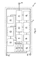
- An in Fig. 1 as a whole with 1 designated triggering device for an airbag in a motor vehicle has a CMOS chip 2 exhibiting electronic component 3, which is fixed to the body 4 of the motor vehicle that at a deformation of the body 4 forces of the body 4 on the CMOS Chip 2 are transmitted.
- CMOS chip 2 a plurality of their main measuring direction transverse to each other arranged force sensors 5 are integrated by means of a standard CMOS, each having a measuring signal output 6, which is connected to an evaluation device 7, which is also integrated into the CMOS chip 2 , Measuring signals for different components of a force acting on the CMOS chip 2 are present at the measuring signal outputs 6.
- the components may be, for example, the x, y, and z components of the force in a Cartesian coordinate system.
- the force sensors 5 each have a Wheatstone bridge whose bridge resistances are formed by piezoelectric elements. When there is a force acting on the CMOS chip 2, a respective voltage dependent on the force is applied to the individual measurement signal outputs 6.
- the evaluation device 7 has an output terminal 8, to which a triggering signal for the airbag can be applied as a function of the measurement signals of the force sensors 5.
- the measurement signal outputs 6 are each connected via an analog / digital converter 9 to an input of a signal processor 10.
- the analog / digital converter 9 is connected to a reference voltage source 11, which is integrated in the CMOS chip 2.
- a non-volatile data memory 12 such as an EEPROM connected, in which at least one tripping characteristic is stored.
- the tripping characteristic can e.g. include a threshold for the slew rate of the measurement signals.
- the measured signals and / or measured values derived therefrom are compared with the at least one tripping characteristic value. Depending on the result of this comparison, the trigger signal is generated and applied to the output terminal 8.
- a temperature sensor 13 is also integrated, which is connected to the signal processor 10 to compensate for changes occurring in temperature fluctuations of the measuring signals.
- the CMOS chip 2 has power supply terminals 14, which are connected to a not shown in the drawing on-board voltage source of the motor vehicle, for example with a car battery.
- a monitoring device 15 is integrated for the supply voltage, which is connected to the power supply terminals 14 and a locking device 16. With the help of the locking device, the reading of the data memory 12 is disabled when applied to the power supply terminals 14 too low electrical operating voltage.
- a BUS interface 17 is integrated, which is compatible to the PSI5 standard.
- the bus interface 17 is connected to the output terminal 8 for outputting the triggering signal to the signal processor 10 and the output terminal 8.
- a diagnostic device 18, which is integrated in the CMOS chip 2 is connected to the BUS interface 17. With the aid of the diagnostic device 18, the operating state of the component 3 and in particular the occurrence of errors can be monitored. If required and / or on request, a corresponding status signal can be sent to the BUS.
- an oscillator 19 is integrated in the CMOS chip 2.
- the oscillator 19 is connected to clock signal inputs of the analog / digital converter 9, the signal processor 10 and the BUS interface 17.
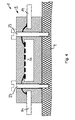
- the CMOS chip is planar over an adhesive layer 20 extending approximately parallel to its main extension plane and frictionally connected to a first surface portion 21 a of the vehicle body 4.
- the consisting of the CMOS chip 2 and the adhesive layer 20 arrangement is overmolded with a solidified potting compound 22 which adheres to the adhesive layer 20 laterally bounding second surface portion 21 b of the vehicle body 4 and seals against it.
- the CMOS chip 2 is encapsulated with a potting compound 22, which forms a housing.
- the potting compound 22 has a plurality of laterally spaced holes, through each of which a fastener 23, namely a screw is passed.
- the fastening element 23 has at its one end a threaded portion screwed to the body 4 and engages with its other end the edge surrounding the perforation of the potting compound 22. As a result, the component 3 is pressed against the body 4.
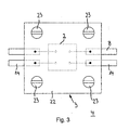
- Fig. 3 It can be seen that the CMOS chip 2 is arranged between the fastening elements 23.
- the component 3 is covered by a plate-shaped holding part 24 which is clamped on both sides of the electronic component 3 by means of screws 25 to the body 2. Between the screws 25, the holding part 24 is supported via the electronic component 3 against the body 2. In this case, the component 3 is flat against the body 2 to the plant.
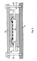
- the CMOS chip 2 can also be encapsulated with a potting compound 22 which adheres to the body 4 frictionally and perforations 26 passes through the body 4.
- the potting compound 22 engages behind the edge region of the perforations 26 in a form-fitting manner on the side of the body 4 facing away from the CMOS chip 2.
Abstract
Description
Die Erfindung betrifft eine Auslösevorrichtung für eine Sicherheitseinrichtung in einem Kraftfahrzeug, insbesondere für einen Airbag, mit einem mindestens einen Kraftsensor aufweisenden elektrischen Bauteil, das derart an der Karosserie des Kraftfahrzeugs befestigt ist, dass an einen Messsignalausgang des Kraftsensors ein von der Deformation der Karosserie abhängiges Messsignal anlegbar ist, und mit einer mit dem Messsignalausgang verbundenen Auswerteeinrichtung zu Verarbeitung des Messsignals.The invention relates to a triggering device for a safety device in a motor vehicle, in particular for an airbag, having an electrical component having at least one force sensor, which is fastened to the body of the motor vehicle such that a measurement signal output of the force sensor is dependent on the deformation of the body measurement signal can be applied, and with an evaluation device connected to the measurement signal output for processing the measurement signal.
Eine derartige Auslösevorrichtung ist aus
Es besteht deshalb die Aufgabe, eine Auslöseeinrichtung der eingangs genannten Art zu schaffen, die kostengünstig herstellbar ist.It is therefore the object to provide a triggering device of the type mentioned, which is inexpensive to produce.
Diese Aufgabe wird dadurch gelöst, dass der Kraftsensor mindestens ein Piezoelement aufweist, das zusammen mit der Auswerteeinrichtung monolithisch in einen CMOS-Chip integriert ist. Dabei wird unter einem Piezoelement insbesondere ein piezoresitives Element verstanden. Das Piezoelement kann aber auch derart ausgestaltet sein, dass es bei Einwirkung einer Kraft eine elektrische Spannung erzeugt. Unter einem CMOS-Chip wird auch ein Bi-CMOS-Chip verstanden, in den zusätzlich zu mindestens einem CMOS-Bauelement wenigstens ein bipolares Bauelement integriert ist. Ferner wird unter einem CMOS-Chip auch ein sogenanntes BCDMOS verstanden, in das mindestens ein DMOS-Transistor Integriert sit.This object is achieved in that the force sensor has at least one piezoelectric element which is monolithically integrated into a CMOS chip together with the evaluation device. In this case, a piezo element is understood in particular to be a piezoresitive element. However, the piezoelectric element can also be designed such that it is under the action of a force an electrical voltage generated. A CMOS chip is also understood to mean a Bi-CMOS chip in which at least one bipolar component is integrated in addition to at least one CMOS component. Furthermore, a CMOS chip is also understood to be a so-called BCDMOS into which at least one DMOS transistor is integrated.
Der mindestens eine Kraftsensor und die Auswerteeinrichtung können dann mit einem Standard-CMOS-Prozess kostengünstig in großer Stückzahl als CMOS-Chip hergestellt werden, wobei auch die elektrischen Verbindungsleitungen zwischen dem Kraftsensor und der Auswerteeinrichtung in den CMOS-Chip integriert werden können. Die Auswerteeinrichtung umfasst bevorzugt zumindest einen Filter für das Messsignal des Piezoelements. Das gefilterte Messsignal, das vorzugsweise eine geringeres Datenvolumen aufweist als das ungefilterte Messsignal, kann dann zu einem weiteren Halbleiterchip übertragen werden, um dort in Abhängigkeit von dem gefilterten Messsignal und ggf dem gefilterten Messsignal mindestens eines weiteren, ein Piezoelement und eine Auswerteeinrichtung aufweisenden CMOS-Chips ein Auslösesignal für die Sicherheitseinrichtung zu erzeugen.The at least one force sensor and the evaluation device can then be manufactured inexpensively in large quantities as a CMOS chip using a standard CMOS process, wherein the electrical connection lines between the force sensor and the evaluation device can also be integrated into the CMOS chip. The evaluation device preferably comprises at least one filter for the measurement signal of the piezoelectric element. The filtered measurement signal, which preferably has a smaller data volume than the unfiltered measurement signal, can then be transmitted to a further semiconductor chip in order there to depend on the filtered measurement signal and possibly the filtered measurement signal of at least one further, a piezoelectric element and an evaluation CMOS chip to generate a trigger signal for the safety device.
Bei einer vorteilhaften Ausgestaltung der Erfindung weist der CMOS-Chip mehrere Piezoelemente auf, die vorzugsweise zu einer Brückenschaltung, insbesondere einer Wheatstone Brücke miteinander verbunden sind. Dadurch können Veränderungen des Messsignals, die auf Temperaturschwankungen und/oder Toleranzen in den Piezoelementen zurückzuführen sind, weitestgehend vermieden werden. Gegebenfalls ist es sogar möglich, dass zur Kompensation einer eventuell noch verbleibenden Abhängigkeit des Messsignals von der Temperatur in den CMOS-Chip eine einen Temperatursensor aufweisende Kompensationsschaltung integriert ist. Die Brückenschaltung kann auch softwaremäßig nachgebildet sein, wobei die Messsignale mehrerer Piezoelemente getrennt voneinander erfasst und mit Hilfe eines Mikrocomputers miteinander verknüpft werden.In an advantageous embodiment of the invention, the CMOS chip on a plurality of piezoelectric elements, which are preferably connected to a bridge circuit, in particular a Wheatstone bridge with each other. As a result, changes in the measurement signal due to temperature fluctuations and / or tolerances in the piezoelectric elements can be largely avoided. Optionally, it is even possible that a temperature sensor having a compensation circuit is integrated to compensate for any remaining dependence of the measurement signal from the temperature in the CMOS chip. The bridge circuit can also be simulated by software, wherein the measurement signals of a plurality of piezo elements are detected separately from each other and linked together using a microcomputer.
Bei einer bevorzugten Ausführungsform der Erfindung hat die Auswerteeinrichtung einen nicht flüchtigen Datenspeicher, in dem mindestens ein Auslösekennwert gespeichert ist, wobei die Auswerteeinrichtung eine Vergleichseinrichtung zum Vergleichen des mindestens einen Auslösekennwerts mit dem Messsignal aufweist, und wobei die Auswerteeinrichtung derart ausgestaltet ist, dass ein Auslösesignal in Abhängigkeit von dem Ergebnis dieses Vergleichs generierbar ist. Als Datenspeicher ist bevorzugt ein E2-Prom vorgesehen. Der CMOS-Chip kann dann auf einfache Weise an unterschiedliche Kraftfahrzeuge und/oder unterschiedliche Einbausituationen in einem Kraftfahrzeug angepasst werden, indem In den Datenspeicher eine oder mehrere entsprechende Kenngröße einprogrammiert wird (werden), die den CMOS-Chip an die jeweils gewünschte Auslösecharakteristik anpassen. Somit kann für unterschiedliche Anwendungsfälle der gleiche CMOS-Chip verwendet werden.In a preferred embodiment of the invention, the evaluation device has a non-volatile data memory in which at least one tripping characteristic value is stored, wherein the evaluation device has a comparison device for comparing the at least one tripping characteristic value with the measurement signal, and wherein the evaluation device is configured such that a tripping signal in Depending on the result of this comparison can be generated. As a data store Preferably, an E 2 -Prom is provided. The CMOS chip can then be adapted in a simple manner to different motor vehicles and / or different installation situations in a motor vehicle by programming one or more corresponding characteristics into the data memory, which adapt the CMOS chip to the respective desired triggering characteristic. Thus, the same CMOS chip can be used for different applications.
Vorteilhaft ist, wenn der CMOS-Chip mehrere mit der Auswerteeinrichtung verbundene Piezoelemente aufweist, mit denen Kraft-Messsignale für mindestens zwei quer zueinander angeordnete Hauptmessrichtungen messbar sind, und wenn die Auswerteeinrichtung derart ausgestaltet ist, dass das Auslösesignal in Abhängigkeit vom Betrag, der Änderungsgeschwindigkeit und/oder der Richtung eines aus den Messsignalen gebildeten resultierenden Messsignals generierbar ist. Dadurch Ist es möglich, das Auslösesignal nur beim Auftreten bestimmter Deformationen der Fahrzeug-Karosserie, wie z.B. bei einem Seitenaufprall und/oder einem Frontalaufprall zu aktivieren.It is advantageous if the CMOS chip has a plurality of piezoelectric elements connected to the evaluation device, with which force measuring signals for at least two main measuring directions arranged transversely to one another can be measured, and if the evaluation device is configured such that the triggering signal depends on the magnitude, the rate of change and / or the direction of a resulting measurement signal formed from the measurement signals can be generated. As a result, it is possible to apply the triggering signal only when certain deformations of the vehicle bodywork, such as the vehicle body, occur. to activate in the event of a side impact and / or a frontal impact.
Zweckmäßigerweise hat die Auslösevorrichtung mindestens zwei Piezoelemente, die unter einem Winkel von etwa 45° zueinander angeordnet sind, wobei zumindest eines dieser Piezoelemente mit seiner Hauptmessrichtung vorzugsweise parallel zur Ausrichtung der Kristalle im CMOS-Chip und/oder zu einem Randbereich und/oder einer Kante des CMOS-Chips angeordnet ist. Mit dem mit seiner Messrichtung in der einen Richtung angeordneten Piezoelement wird hauptsächlich die Oberflächenspannung des CMOS-Chips gemessen, während mit dem mit seiner Messrichtung in die andere Richtung angeordneten Piezoelement hauptsächlich die Scherspannung im CMOS-Chip bzw. das auf den CMOS-Chip einwirkende Drehmoment gemessen wird. In Abhängigkeit von den Messsignalen für die Oberflächenspannung und die Scherspannung kann dann auf die Art der Deformation der Karosserie geschlossen werden. Dadurch ist es möglich, die Sicherheitseinrichtung nur bei bestimmten Deformationsmustern auszulösen. Die Piezoelemente sind vorzugsweise derart angeordnet, dass die Scherspannung und die Oberflächenspannung jeweils in drei quer und vorzugsweise orthogonal zueinander verlaufenden Achsen (a, b, c bzw. x, y, z) gemessen werden können.Conveniently, the triggering device has at least two piezoelectric elements which are arranged at an angle of approximately 45 ° to each other, wherein at least one of these piezoelectric elements with its main measuring direction preferably parallel to the orientation of the crystals in the CMOS chip and / or to an edge region and / or edge of the CMOS chips is arranged. With the piezoelectric element arranged with its measuring direction in one direction, the surface voltage of the CMOS chip is mainly measured, while with the piezoelectric element arranged with its measuring direction in the other direction, mainly the shearing voltage in the CMOS chip or the torque acting on the CMOS chip is measured. Depending on the measuring signals for the surface tension and the shear stress can then be concluded on the type of deformation of the body. This makes it possible to trigger the safety device only with certain deformation patterns. The piezoelectric elements are preferably arranged such that the shear stress and the surface tension in each case in three transversely and preferably orthogonally extending axes (a, b, c or x, y, z) can be measured.
Bei einer bevorzugten Ausgestaltung der Erfindung ist der CMOS-Chip über mindestens eine vorzugsweise etwa parallel zu seiner Haupterstreckungsebene verlaufende Klebstoffschicht flächig und kraftschlüssig mit einem ersten Oberflächenbereich der Fahrzeug-Karosserie verbunden, wobei die aus dem CMOS-Chip und der mindestens einen Klebstoffschicht bestehende Anordnung mit einer verfestigten Vergussmasse überdeckt ist, die dicht mit einem die Klebstoffschicht seitlich umgrenzenden zweiten Oberflächenbereich der Fahrzeug-Karosserie verbunden ist. Der CMOS-Chip kann dann bei der Fertigung der Fahrzeug-Karosserie direkt auf diese aufgeklebt und danach derart mit der Vergussmasse umspritzt werden, dass der CMOS-Chip durch die Vergussmasse und die Fahrzeug-Karosserie umkapselt wird. Bei einer Deformation der Karosserie werden die auf die Karosserie einwirkenden Deformationskröfte über die Klebstoffschicht direkt auf den CMOS-Chip und somit den mindestens einen Kraftsensor übertragen. Die Vergussmasse besteht bevorzugt aus einem weichen Material, dessen Nachgiebigkeit so gewählt ist, dass bei einer Deformation der Karosserie die Kräfte hauptsächlich über die Klebstoffschicht von der Karosserie auf den CMOS-Chip übertragen werden.In a preferred embodiment of the invention, the CMOS chip via at least one preferably approximately parallel to its main extension plane extending adhesive layer and non-positively connected to a first surface region of the vehicle body, wherein the consisting of the CMOS chip and the at least one adhesive layer arrangement with a solidified potting compound is covered, which is tightly connected to a side of the adhesive layer adjacent the second surface region of the vehicle body. The CMOS chip can then be adhered directly to the vehicle body during manufacture and then molded with the potting compound such that the CMOS chip is encapsulated by the potting compound and the vehicle body. In the event of a deformation of the body, the deformation forces acting on the body are transmitted via the adhesive layer directly to the CMOS chip and thus to the at least one force sensor. The potting compound is preferably made of a soft material whose compliance is chosen so that in a deformation of the body, the forces are transmitted mainly via the adhesive layer of the body to the CMOS chip.
Zweckmäßigerweise ist der CMOS-Chip über mindestens zwei gestapelte Klebstoffschichten mit dem ersten Oberflächenbereich der Fahrzeug-Karosserie verbunden, wobei zwischen diesen Klebstoffschichten eine Metallfolie angeordnet ist. Die Metallfolie ermöglicht dabei eine gut wärmeleitenden Verbindung zwischen dem CMOS-Chip und der Karosserie, so dass in dem CMOS-Chip auftretende Verlustwärme über die Karosserie großflächig an die Umgebung abgeleitet werden kann.Conveniently, the CMOS chip is connected via at least two stacked adhesive layers to the first surface region of the vehicle body, wherein a metal foil is arranged between these adhesive layers. The metal foil allows a good heat-conducting connection between the CMOS chip and the body, so that in the CMOS chip occurring heat loss can be derived over the body over a large area to the environment.
Bei einer vorteilhaften Ausführungsform der Erfindung ist der CMOS-Chip mit einer diesen dicht umschließenden Vergussmasse umspritzt, wobei die Vergussmasse mindestens zwei seitlich voneinander beabstandete Lochungen aufweist, durch die Befestigungselemente hindurchgeführt sind, über welche das durch den CMOS-Chip und die Vergussmasse gebildete elektronische Bauteil kraftschlüssig mit der Karosserie verbunden ist. Dabei sind als Befestigungselemente bevorzugt Schrauben vorgesehen. Die Auslösevorrichtung kann dann im Servicefall leicht von der Karosserie gelöst und durch ein entsprechendes Ersatzteil ersetzt werden. Der CMOS-Chip ist bevorzugt zwischen den Lochungen angeordnet, so dass auf die Karosserie einwirkende Deformationskräfte über die Befestigungselemente und die vorzugsweise harte Vergussmasse gut auf den CMOS-Chip übertragen werden können.In an advantageous embodiment of the invention, the CMOS chip is encapsulated with a sealing encapsulation that closely surrounds it, wherein the encapsulant has at least two laterally spaced holes through which fastening elements are passed, via which the electronic component formed by the CMOS chip and the encapsulation compound positively connected to the body. In this case, screws are preferably provided as fastening elements. The triggering device can then be easily detached from the body during servicing and replaced by a corresponding replacement part. The CMOS chip is preferably arranged between the perforations, so that forces acting on the body deformation forces on the fasteners and the preferably hard potting compound can be transferred well to the CMOS chip.
Bei einer anderen vorteilhaften Ausführungsform der Erfindung ist der CMOS-Chip über eine über eine an der Karosserie (4) anhaftende Vergussmasse kraftschlüssig mit der Karosserie des Kraftfahrzeugs verbunden, wobei die Vergussmasse vorzugsweise zwischen dem CMOS-Chip und der Karosserie angeordnet ist und/oder die Karosserie hintergreift. Dabei ist es sogar möglich dass die Vergussmasse mindestens eine in einer Wandung der Karosserie vorgesehene Lochung durchsetzt und einen Randbereich dieser Lochung an der dem CMOS-Chip abgewandten Seite der Karosserie-Wandung hintergreift.In another advantageous embodiment of the invention, the CMOS chip is frictionally connected via a to the body (4) adhering potting compound with the body of the motor vehicle, wherein the potting compound is preferably disposed between the CMOS chip and the body and / or Body engages behind. It is even possible that the potting compound passes through at least one provided in a wall of the body perforation and engages behind an edge region of this perforation on the side facing away from the CMOS chip body wall.
Bei einer anderen Ausgestaltung der Erfindung Ist das Bauteil von einem vorzugsweise plattenförmigen Halteteil überdeckt, wobei das Halteteil beidseits des elektronischen Bauteils an Befestigungsstellen mit der Karosserie verspannt und zwischen den Befestigungsstellen über das elektronische Bauteil gegen die Karosserie abgestützt ist. Das aus der Vergussmasse oder der Umkapselung und dem CMOS-Chip gebildete Bauteil wird dann durch das Halteteil vorzugsweise flächig an die Karosserie angepresst und verformt sich bei einer Deformation der Karosserie zusammen mit dieser.In another embodiment of the invention, the component is covered by a preferably plate-shaped holding part, wherein the holding part is clamped on both sides of the electronic component at attachment points with the body and is supported between the attachment points on the electronic component against the body. The component formed from the potting compound or the encapsulation and the CMOS chip is then pressed by the holding member preferably flat against the body and deforms in a deformation of the body together with this.
Vorteilhaft ist, wenn das Bauteil an einem einen Teil der Außenhaut der Karosserie bildenden Karosseriewandung befestigt ist, insbesondere an deren der Fahrzeugaußenseite abgewandten Rückseite. Auf die Außenhaut der Karosserie einwirkende Deformationskröfte können dann bereits zu Beginn der Deformation direkt von dem mindestens einen Piezoelement gemessen werden.It is advantageous if the component is fastened to a bodywork forming a part of the outer skin of the body, in particular on its rear side facing away from the vehicle exterior. Deformation forces acting on the outer skin of the body can then be measured directly at the beginning of the deformation by the at least one piezoelectric element.
Bei einer bevorzugten Ausgestaltung der Erfindung ist in den CMOS-Chip ein BUS-Interface integriert, das vorzugsweise zum PSI5-Standard kompatibel ist.In a preferred embodiment of the invention, a BUS interface is integrated in the CMOS chip, which is preferably compatible to the PSI5 standard.
Bei einer bevorzugten Ausführungsform der Erfindung weist die Auslösevorrichtung eine Diagnoseeinrichtung auf, die Mittel zum Detektieren eines im Messsignal enthaltenen Signalanteils hat, der durch Vibrationen hervorgerufen wird, die durch einen Antriebsmotor des Kraftfahrzeugs verursacht werden, insbesondere durch einen Verbrennungsmotor. Mit Hilfe der Diagnoseeinrichtung kann dann überprüft werden, ob der Kraftsensor funktionsfähig und kraftschlüssig mit der Karosserie verbunden ist. Sollte sich der Kraftsensor einmal von der Karosserie ablösen, würden die Motorvibrationen nicht mehr oder nur noch zu einem kleinen Teil auf den Kraftsensor übertragen. Dieser Defekt könnte dann mit Hilfe der Diagnoseeinrichtung festgestellt und ggf. zur Anzeige gebracht werden. Die Diagnoseeinrichtung kann außerdem Mittel zum überprüfen der elektrischen Betriebsspannung des CMOS-Chips und/oder Funktionsfähigkeit des BUS-interface aufweisen. Beim Feststellen des Defekts kann die Sicherheitseinrichtung auf ein Notbetriebsprogramm umgeschaltet werden.
Vorteilhaft ist, wenn in dem CMOS-Chip mindestens ein weiterer, sich von dem Kraftsensor unterscheidender Sensor, insbesondere ein Temperatursensor, ein Sensor zur Messung einer elektrischen Kapazität, ein Magnetfeldsensor und/oder ein Feuchtigkeitssensor integriert ist. Die zusätzlichen Sensoren können zu Diagnosezwecken und/oder zur Kompensation des Messsignals gegen Störeinflüsse mit der Auswerteeinrichtung verbunden sein. Mit Hilfe des kapazitiven Sensors kann der Abstand des CMOS-Chip zur Karosserie und somit das Vorhanden sein der kraftschlüssigen Verbindung zur Karosserie überprüft werden.In a preferred embodiment of the invention, the triggering device has a diagnostic device which has means for detecting a signal component contained in the measurement signal, which is caused by vibrations caused by a drive motor of the motor vehicle, in particular by an internal combustion engine. With the help of the diagnostic device can then be checked be whether the force sensor is operatively and non-positively connected to the body. If the force sensor separates once from the body, the engine vibrations would no longer or only to a small extent transferred to the force sensor. This defect could then be detected with the help of the diagnostic device and possibly displayed. The diagnostic device may also comprise means for checking the electrical operating voltage of the CMOS chip and / or functionality of the bus interface. Upon detection of the defect, the safety device can be switched to an emergency operation program.
It is advantageous if in the CMOS chip at least one further, different from the force sensor sensor, in particular a temperature sensor, a sensor for measuring an electrical capacitance, a magnetic field sensor and / or a moisture sensor is integrated. The additional sensors can be connected to the evaluation device for diagnostic purposes and / or for compensation of the measurement signal against interference. With the help of the capacitive sensor, the distance of the CMOS chip to the body and thus the presence of the non-positive connection to the body can be checked.
Nachfolgend sind Ausführungsbeispiele der Erfindung anhand der Zeichnung näher erläutert. Es zeigt
- Fig, 1
- einen Querschnitt durch einen flächig auf eine Karosserie aufgeklebten CMOS-Chip, in den piezoresistive Kraftsensoren und eine Auswerteeinrichtung monolithisch integriert sind,
- Fig. 2
- ein Blockschaltbild eines CMOS-Chips, in den eine Schaltung zum Auslösen eines Airbags in einem Kraftfahrzeug integriert Ist,
- Fig. 3
- ein Aufsicht auf ein einen CMOS-Chip enthaltendes elektrisches Bauteil, das an mehreren Stellen mit einer Karosserie verschraubt Ist,
- Fig. 4
- einen Querschnitt durch die in
Fig. 3 gezeigte Anordnung, - Fig. 5
- eine Seitenansicht eines einen CMOS-Chip enthaltenden elektrischen Bauteils, das zwischen einem plattenförmigen Halteteil und einer Karosserie eingespannt ist, und
- Fig. 6
- einen Querschnitt durch einen CMOS-Chip, der mit einer die Karosserie formschlüssig hintergreifenden Vergussmasse umkapselt ist.
- Fig, 1
- a cross-section through a surface adhered to a body CMOS chip, are integrated monolithically in the piezoresistive force sensors and an evaluation,
- Fig. 2
- a block diagram of a CMOS chip, in which a circuit for triggering an airbag is integrated in a motor vehicle,
- Fig. 3
- a plan view of an electrical component containing a CMOS chip, which is bolted to a body in several places,
- Fig. 4
- a cross section through the in
Fig. 3 shown arrangement, - Fig. 5
- a side view of a CMOS chip-containing electrical component, which is clamped between a plate-shaped holding part and a body, and
- Fig. 6
- a cross section through a CMOS chip, which is encapsulated with a body engaging behind the form-fitting potting compound.
Eine in
In den CMOS-Chip 2 sind mittels eines Standard-CMOS-Prozesses mehrere mit ihrer Hauptmessrichtung quer zueinander angeordnete Kraftsensoren 5 Integriert, die jeweils einen Messsignalausgang 6 aufweisen, der mit einer Auswerteeinrichtung 7 verbunden ist, die ebenfalls in den CMOS-Chip 2 integriert ist. An den Messsignalausgängen 6 liegen Messsignale für unterschiedliche Komponenten einer auf den CMOS-Chip 2 einwirkenden Kraft an. Die Komponenten können beispielsweise die x-, y- und z-Komponente der Kraft in einem kartesischen Koordinatensystem sein.In the CMOS chip 2 a plurality of their main measuring direction transverse to each other arranged force sensors 5 are integrated by means of a standard CMOS, each having a measuring signal output 6, which is connected to an evaluation device 7, which is also integrated into the
Die Kraftsensoren 5 haben jeweils eine Wheatstone Brücke, deren Brückenwiderstände durch Piezoelemente gebildet sind. Bei einer Krafteinwirkung auf den CMOS-Chip 2 liegt an den einzeinen Messsignalausgängen 6 jeweils eine von der Kraft abhängige elektrische Spannung an.The force sensors 5 each have a Wheatstone bridge whose bridge resistances are formed by piezoelectric elements. When there is a force acting on the
Die Auswerteeinrichtung 7 hat einen Ausgangsanschluss 8, an dem in Abhängigkeit von den Messsignalen der Kraftsensoren 5 ein Auslösesignal für den Airbag anlegbar ist. In
An dem Signalprozessor 10 Ist ein nicht flüchtiger Datenspeicher 12, wie z.B. ein EEPROM angeschlossen, in dem mindestens ein Auslösekennwert gespeichert ist.At the
Der Auslösekennwert kann z.B. einen Grenzwert für die Anstiegsgeschwindigkeit der Messsignale umfassen. Mit Hilfe des Signalprozessors 10 werden die Messsignale und/oder daraus abgeleitete Messwerte mit dem mindestens ein Auslösekennwert verglichen. In Abhängigkeit von dem Ergebnis dieses Vergleichs wird das Auslösesignal erzeugt und an den Ausgangsanschluss 8 angelegt.The tripping characteristic can e.g. include a threshold for the slew rate of the measurement signals. With the aid of the
In den CMOS-Chip 2 ist außerdem ein Temperatursensor 13 integriert, der zur Kompensation von bei Temperaturschwankungen auftretenden Veränderungen der Messsignale mit dem Signalprozessor 10 verbunden ist.In the
Der CMOS-Chip 2 hat Spannungsversorgungsanschlüsse 14, die mit einer in der Zeichnung nicht näher dargestellten Bordspannungsquelle des Kraftfahrzeugs verbunden sind, beispielsweise mit einer Autobatterie. In den CMOS-Chip 2 ist eine Überwachungseinrichtung 15 für die Versorgungsspannung integriert, die mit den Spannungsversorgungsanschlüssen 14 und einer Verriegelungseinrichtung 16 verbunden ist. Mit Hilfe der Verriegelungseinrichtung wird das Auslesen des Datenspeichers 12 gesperrt, wenn an den Spannungsversorgungsanschlüsse 14 eine zu geringe elektrische Betriebsspannung anliegt.The
In den CMOS-Chip ist ein BUS-Interface 17 integriert ist, das zum PSI5-Standard kompatibel ist. Das BUS-Interface 17 ist zur Ausgabe des Auslösesignals an den Ausgangsanschluss 8 mit dem Signalprozessor 10 und dem Ausgangsanschluss 8 verbunden. An dem BUS-Interface 17 ist außerdem eine Diagnoseeinrichtung 18 angeschlossen, die in den CMOS-Chip 2 integriert ist. Mit Hilfe der Diagnoseeinrichtung 18 können der Betriebszustand der Bauteils 3 und insbesondere das Auftreten von Fehlern überwacht werden. Bei Bedarf und/oder auf Anforderung kann ein entsprechendes Statussignal auf den BUS gesendet werden.In the CMOS chip, a
Erwähnt werden soll noch, dass zum Erzeugen eines Taktsignals ist ein Oszillator 19 in den CMOS-Chip 2 integriert ist. Der Oszillator 19 ist mit Taktsignaleingängen des Analog-/Digital-Konverters 9, des Signalprozessors 10 und des BUS-Interfaces 17 verbunden.It should also be mentioned that for generating a clock signal, an
Bei dem In
Bei dem Ausführungsbeispiel gemäß
Bei dem in
Wie in
Claims (14)
Priority Applications (4)
| Application Number | Priority Date | Filing Date | Title |
|---|---|---|---|
| EP07014972A EP2020339B1 (en) | 2007-07-31 | 2007-07-31 | Activation device for the safety device in a motor vehicle |
| EP08013089A EP2020340B1 (en) | 2007-07-31 | 2008-07-21 | Activation device for the safety device in a motor vehicle |
| JP2008193146A JP2009035251A (en) | 2007-07-31 | 2008-07-28 | Activation device for safety device in automobile |
| US12/182,658 US7845677B2 (en) | 2007-07-31 | 2008-07-30 | Triggering device for a safety device in an automotive vehicle |
Applications Claiming Priority (1)
| Application Number | Priority Date | Filing Date | Title |
|---|---|---|---|
| EP07014972A EP2020339B1 (en) | 2007-07-31 | 2007-07-31 | Activation device for the safety device in a motor vehicle |
Publications (2)
| Publication Number | Publication Date |
|---|---|
| EP2020339A1 true EP2020339A1 (en) | 2009-02-04 |
| EP2020339B1 EP2020339B1 (en) | 2012-03-28 |
Family
ID=38893989
Family Applications (2)
| Application Number | Title | Priority Date | Filing Date |
|---|---|---|---|
| EP07014972A Expired - Fee Related EP2020339B1 (en) | 2007-07-31 | 2007-07-31 | Activation device for the safety device in a motor vehicle |
| EP08013089A Expired - Fee Related EP2020340B1 (en) | 2007-07-31 | 2008-07-21 | Activation device for the safety device in a motor vehicle |
Family Applications After (1)
| Application Number | Title | Priority Date | Filing Date |
|---|---|---|---|
| EP08013089A Expired - Fee Related EP2020340B1 (en) | 2007-07-31 | 2008-07-21 | Activation device for the safety device in a motor vehicle |
Country Status (3)
| Country | Link |
|---|---|
| US (1) | US7845677B2 (en) |
| EP (2) | EP2020339B1 (en) |
| JP (1) | JP2009035251A (en) |
Cited By (2)
| Publication number | Priority date | Publication date | Assignee | Title |
|---|---|---|---|---|
| WO2017207243A1 (en) * | 2016-06-02 | 2017-12-07 | Robert Bosch Gmbh | Safety device for a vehicle, vehicle, method for operating a safety device of a vehicle |
| DE112013004598B4 (en) | 2012-09-20 | 2020-01-02 | Korea Institute Of Industrial Technology | Airbag sensor module and vehicle body with an integrated airbag sensor module |
Families Citing this family (15)
| Publication number | Priority date | Publication date | Assignee | Title |
|---|---|---|---|---|
| DE102011100487A1 (en) * | 2011-05-04 | 2012-11-08 | Micronas Gmbh | Integrated passive component |
| DE102011100485B4 (en) | 2011-05-04 | 2016-04-28 | Micronas Gmbh | Integrated passive component and its use |
| JP2013118937A (en) * | 2011-12-07 | 2013-06-17 | Fujifilm Corp | Electronic endoscope, method for manufacturing the same, and electronic endoscope system |
| EP2657691B1 (en) * | 2012-04-25 | 2018-08-29 | E+E Elektronik Ges.m.b.H. | Moisture sensor assembly |
| DE102012216529B4 (en) * | 2012-09-17 | 2020-09-17 | Robert Bosch Gmbh | Method for triggering at least one personal protection device as well as system and computer program product for carrying out the method |
| JP5870989B2 (en) * | 2013-12-03 | 2016-03-01 | 株式会社デンソー | Vehicle pressure detection device |
| US9260071B2 (en) * | 2014-03-11 | 2016-02-16 | Trw Automotive U.S. Llc | Apparatus for snap mounting a crash sensor |
| US9470595B2 (en) | 2014-08-29 | 2016-10-18 | Trw Automotive U.S. Llc | Apparatus for dry side mounting a crash pressure sensor |
| JP6369415B2 (en) * | 2015-07-28 | 2018-08-08 | 株式会社デンソー | Vehicle collision sensor and vehicle collision detection device using the same |
| JP2017030709A (en) * | 2015-08-06 | 2017-02-09 | 株式会社デンソー | Vehicle collision detecting apparatus |
| US10093181B1 (en) | 2015-09-30 | 2018-10-09 | Waymo Llc | Occupant facing vehicle display |
| CN105547880A (en) * | 2015-12-31 | 2016-05-04 | 广东科学技术职业学院 | Fast metal plate strength detecting device and detecting method thereof |
| JP6515881B2 (en) * | 2016-06-28 | 2019-05-22 | 株式会社デンソー | Vehicle collision detector |
| DE102017129068B4 (en) * | 2017-12-06 | 2022-01-20 | Webasto SE | Distributed sensor system for detecting body parts and people in the danger areas of a convertible top |
| CN108709678B (en) * | 2018-07-26 | 2024-02-06 | 宜博科测控科技(苏州)有限公司 | Automobile door sensor detection device and automobile door sensor |
Citations (5)
| Publication number | Priority date | Publication date | Assignee | Title |
|---|---|---|---|---|
| DE4237404A1 (en) | 1992-11-05 | 1994-05-11 | Base Ten Systems Electronics G | Vehicle side airbag trigger control - involves measuring degree and rate of deformation of strut or plate using pref. electric strain gauge |
| EP0978425A1 (en) * | 1998-08-06 | 2000-02-09 | Volkswagen Aktiengesellschaft | Method and apparatus for the deployment of at least one airbag using pressure sensitive sensors |
| EP1604870A2 (en) | 2004-06-11 | 2005-12-14 | Robert Bosch GmbH | Hybrid impact sensor |
| DE102005014013A1 (en) * | 2005-03-26 | 2006-09-28 | Conti Temic Microelectronic Gmbh | Vehicle sensor for e.g. passenger protection system of automobile, has measurement sensor with different direction-dependant sensing characteristics that are predetermined by its geometrical form and polarizations of piezoelectric material |
| US20060241834A1 (en) | 2003-06-25 | 2006-10-26 | Philip Kithil | Crash sensing via piezoelectric sensors |
Family Cites Families (29)
| Publication number | Priority date | Publication date | Assignee | Title |
|---|---|---|---|---|
| DE2212190A1 (en) | 1972-03-14 | 1973-09-27 | Volkswagenwerk Ag | COLLISION SENSOR |
| US4313903A (en) * | 1979-11-19 | 1982-02-02 | Bayer Aktiengesellschaft | Process for injection molding of polyethylene terephthalate compositions at reduced mold temperature |
| US4489110A (en) * | 1982-01-15 | 1984-12-18 | Bayer Aktiengesellschaft | Polyethylene terephthalate moulding compositions having high reflectivity |
| DE3339001A1 (en) * | 1983-07-06 | 1985-01-17 | Bayer Ag, 5090 Leverkusen | THERMOPLASTIC POLYESTER MOLDS WITH HIGH TOUGHNESS |
| DE3716168A1 (en) | 1987-05-14 | 1988-11-24 | Bayerische Motoren Werke Ag | Sensor for a safety device for motor vehicles |
| JP2669552B2 (en) * | 1989-02-07 | 1997-10-29 | ポリプラスチックス株式会社 | Polyester resin composition |
| JP2546149Y2 (en) | 1991-06-19 | 1997-08-27 | 株式会社シマノ | Bicycle pedals |
| DE4309827C2 (en) * | 1993-03-26 | 1995-12-14 | Daimler Benz Ag | Tripping device for a safety device in a vehicle, in particular for a side airbag |
| DE4325414C2 (en) * | 1993-07-29 | 2000-02-17 | Daimler Chrysler Ag | Deformation sensor for a safety device to protect vehicle occupants in the event of a side impact |
| US5882774A (en) * | 1993-12-21 | 1999-03-16 | Minnesota Mining And Manufacturing Company | Optical film |
| DE69818721T2 (en) * | 1997-02-03 | 2004-07-29 | Teijin Ltd. | Polyethylene 2,6-naphthalene dicarboxylate resin, preform and molded bottle made of it |
| EP1548045B1 (en) * | 1998-01-13 | 2009-06-03 | Minnesota Mining And Manufacturing Company | Modified copolyesters |
| US6788463B2 (en) * | 1998-01-13 | 2004-09-07 | 3M Innovative Properties Company | Post-formable multilayer optical films and methods of forming |
| US6808658B2 (en) * | 1998-01-13 | 2004-10-26 | 3M Innovative Properties Company | Method for making texture multilayer optical films |
| US6531230B1 (en) * | 1998-01-13 | 2003-03-11 | 3M Innovative Properties Company | Color shifting film |
| WO2000000548A1 (en) * | 1998-06-26 | 2000-01-06 | Teijin Limited | Aromatic polyester compositions and method for producing molded articles and bottles therefrom |
| US6449093B2 (en) * | 1999-10-12 | 2002-09-10 | 3M Innovative Properties Company | Optical bodies made with a birefringent polymer |
| DE10103047C1 (en) * | 2001-01-24 | 2002-07-25 | Bosch Gmbh Robert | Side impact detection device for automobile uses deformation sensor with sensor element mounted on base plate provided with temperature sensor for detection of rivetting fault |
| US7052762B2 (en) * | 2001-05-24 | 2006-05-30 | 3M Innovative Properties Company | Low Tg multilayer optical films |
| US6991695B2 (en) * | 2002-05-21 | 2006-01-31 | 3M Innovative Properties Company | Method for subdividing multilayer optical film cleanly and rapidly |
| WO2005116915A1 (en) * | 2004-05-22 | 2005-12-08 | 3M Innovative Properties Company | Cards and laminates incorporating multilayer optical films |
| US7288296B2 (en) * | 2004-06-03 | 2007-10-30 | Nitto Denko Corporation | Multilayer optical compensator, liquid crystal display, and process |
| DE102004036501A1 (en) | 2004-07-28 | 2006-03-23 | Daimlerchrysler Ag | Motor vehicle and object e.g. pedestrian, collision detecting device, has collision sensor arranged in deformable exterior area of vehicle and transferable to its initial state after it is released due to force effected on area |
| US7345137B2 (en) * | 2004-10-18 | 2008-03-18 | 3M Innovative Properties Company | Modified copolyesters and optical films including modified copolyesters |
| US7713595B2 (en) * | 2005-10-18 | 2010-05-11 | Nitto Denko Corporation | Optical compensation films produced by a carrier-web-casting process |
| JP5015953B2 (en) * | 2005-12-23 | 2012-09-05 | スリーエム イノベイティブ プロパティズ カンパニー | Multilayer films containing thermoplastic silicone block copolymers |
| US20070298271A1 (en) * | 2006-06-23 | 2007-12-27 | 3M Innovative Properties Company | Multilayer optical film, method of making the same, and transaction card having the same |
| TW200815181A (en) * | 2006-07-18 | 2008-04-01 | 3M Innovative Properties Co | Calendering process for making an optical film |
| US8012571B2 (en) * | 2008-05-02 | 2011-09-06 | 3M Innovative Properties Company | Optical film comprising birefringent naphthalate copolyester having branched or cyclic C4-C10 alkyl units |
-
2007
- 2007-07-31 EP EP07014972A patent/EP2020339B1/en not_active Expired - Fee Related
-
2008
- 2008-07-21 EP EP08013089A patent/EP2020340B1/en not_active Expired - Fee Related
- 2008-07-28 JP JP2008193146A patent/JP2009035251A/en active Pending
- 2008-07-30 US US12/182,658 patent/US7845677B2/en not_active Expired - Fee Related
Patent Citations (5)
| Publication number | Priority date | Publication date | Assignee | Title |
|---|---|---|---|---|
| DE4237404A1 (en) | 1992-11-05 | 1994-05-11 | Base Ten Systems Electronics G | Vehicle side airbag trigger control - involves measuring degree and rate of deformation of strut or plate using pref. electric strain gauge |
| EP0978425A1 (en) * | 1998-08-06 | 2000-02-09 | Volkswagen Aktiengesellschaft | Method and apparatus for the deployment of at least one airbag using pressure sensitive sensors |
| US20060241834A1 (en) | 2003-06-25 | 2006-10-26 | Philip Kithil | Crash sensing via piezoelectric sensors |
| EP1604870A2 (en) | 2004-06-11 | 2005-12-14 | Robert Bosch GmbH | Hybrid impact sensor |
| DE102005014013A1 (en) * | 2005-03-26 | 2006-09-28 | Conti Temic Microelectronic Gmbh | Vehicle sensor for e.g. passenger protection system of automobile, has measurement sensor with different direction-dependant sensing characteristics that are predetermined by its geometrical form and polarizations of piezoelectric material |
Cited By (2)
| Publication number | Priority date | Publication date | Assignee | Title |
|---|---|---|---|---|
| DE112013004598B4 (en) | 2012-09-20 | 2020-01-02 | Korea Institute Of Industrial Technology | Airbag sensor module and vehicle body with an integrated airbag sensor module |
| WO2017207243A1 (en) * | 2016-06-02 | 2017-12-07 | Robert Bosch Gmbh | Safety device for a vehicle, vehicle, method for operating a safety device of a vehicle |
Also Published As
| Publication number | Publication date |
|---|---|
| JP2009035251A (en) | 2009-02-19 |
| EP2020339B1 (en) | 2012-03-28 |
| EP2020340B1 (en) | 2012-03-28 |
| EP2020340A1 (en) | 2009-02-04 |
| US7845677B2 (en) | 2010-12-07 |
| US20090066066A1 (en) | 2009-03-12 |
Similar Documents
| Publication | Publication Date | Title |
|---|---|---|
| EP2020339B1 (en) | Activation device for the safety device in a motor vehicle | |
| EP3304021B1 (en) | Apparatus for sensing a pressure of a fluid medium, and method for manufacturing said apparatus | |
| EP2282914B1 (en) | Control device for passenger protection means for a vehicle and method for assembling a control device for passenger protection means for a vehicle | |
| EP1301762A1 (en) | Piezoelectric sensor | |
| DE112006002206T5 (en) | Fastener integrated sensor | |
| EP3499199B1 (en) | Wim sensor and method for manufacturing the wim sensor | |
| EP2614589B1 (en) | Capacitive distance sensor | |
| WO2014095316A2 (en) | Electronic device and method for producing an electronic device | |
| EP3194897B1 (en) | Moisture detection within a sensor | |
| EP0955524A2 (en) | Mass air flow sensor | |
| DE102011002884A1 (en) | Force-and/or pressure-and/or temperature measuring electronic circuit for use in force-and/or pressure- and/or temperature sensors in brake device of motor car, has semi-bridge elements whose metallic resistors form potential divider | |
| DE102015007375A1 (en) | LINEAR SENSOR DEVICE FOR A VEHICLE | |
| WO2018104511A2 (en) | Joining device, monitoring method and mounting tool for a joining device | |
| DE19831270B4 (en) | Arrangement and method for determining and monitoring the state of stress of a fastening element | |
| DE102007044346A1 (en) | Connecting unit e.g. screw, for use as seat force sensor in vehicle seat for sensing and classifying vehicle occupant, has printed circuit board and sensor system connected with each other in firmly-bonded and positive manner | |
| WO2001096886A1 (en) | Method and device for inspecting the mechanical fastening of a component to a base body | |
| DE112017003236T5 (en) | VEHICLE COLLISION DETECTION DEVICE | |
| EP3242400B1 (en) | Electronic sensor unit for detecting a contact-free actuation of a door or hatch on a motor vehicle | |
| DE202016106885U1 (en) | Connecting device and assembly tool for a connecting device | |
| WO2020126196A1 (en) | Pressure sensor for sensing the pressure of fluid media, and pressure sensor device having a pressure sensor of this type | |
| DE102016220031A1 (en) | Sensor device for a vehicle, motor vehicle | |
| DE102007043070A1 (en) | Measuring circuit for measuring e.g. pressure in brake pressure line of vehicle, has comparator device for comparing potentials at nodes of network and outputting evaluation signal depending on difference of potentials | |
| DE102010031596A1 (en) | Control device for controlling personal protection devices of vehicle, comprises integrated circuit for controlling power source, and primary capacitor, which is connected with primary connection | |
| WO2017054994A1 (en) | Diagnosis of a control device | |
| EP1726964B1 (en) | Method for locally compensating the temperature drift of sensors in the mounted state and device for compensating the temperature drift of a semiconductor acceleration sensor |
Legal Events
| Date | Code | Title | Description |
|---|---|---|---|
| PUAI | Public reference made under article 153(3) epc to a published international application that has entered the european phase |
Free format text: ORIGINAL CODE: 0009012 |
|
| AK | Designated contracting states |
Kind code of ref document: A1 Designated state(s): AT BE BG CH CY CZ DE DK EE ES FI FR GB GR HU IE IS IT LI LT LU LV MC MT NL PL PT RO SE SI SK TR |
|
| AX | Request for extension of the european patent |
Extension state: AL BA HR MK RS |
|
| 17P | Request for examination filed |
Effective date: 20090515 |
|
| AKX | Designation fees paid |
Designated state(s): DE FR GB |
|
| GRAP | Despatch of communication of intention to grant a patent |
Free format text: ORIGINAL CODE: EPIDOSNIGR1 |
|
| RIC1 | Information provided on ipc code assigned before grant |
Ipc: G01L 1/18 20060101ALI20111111BHEP Ipc: B60R 21/0136 20060101AFI20111111BHEP |
|
| GRAS | Grant fee paid |
Free format text: ORIGINAL CODE: EPIDOSNIGR3 |
|
| GRAA | (expected) grant |
Free format text: ORIGINAL CODE: 0009210 |
|
| AK | Designated contracting states |
Kind code of ref document: B1 Designated state(s): DE FR GB |
|
| REG | Reference to a national code |
Ref country code: GB Ref legal event code: FG4D Free format text: NOT ENGLISH |
|
| REG | Reference to a national code |
Ref country code: DE Ref legal event code: R096 Ref document number: 502007009554 Country of ref document: DE Effective date: 20120524 |
|
| PLBE | No opposition filed within time limit |
Free format text: ORIGINAL CODE: 0009261 |
|
| STAA | Information on the status of an ep patent application or granted ep patent |
Free format text: STATUS: NO OPPOSITION FILED WITHIN TIME LIMIT |
|
| 26N | No opposition filed |
Effective date: 20130103 |
|
| REG | Reference to a national code |
Ref country code: DE Ref legal event code: R097 Ref document number: 502007009554 Country of ref document: DE Effective date: 20130103 |
|
| REG | Reference to a national code |
Ref country code: FR Ref legal event code: PLFP Year of fee payment: 10 |
|
| REG | Reference to a national code |
Ref country code: DE Ref legal event code: R082 Ref document number: 502007009554 Country of ref document: DE Representative=s name: KOCH-MUELLER PATENTANWALTSGESELLSCHAFT MBH, DE Ref country code: DE Ref legal event code: R081 Ref document number: 502007009554 Country of ref document: DE Owner name: TDK-MICRONAS GMBH, DE Free format text: FORMER OWNER: MICRONAS GMBH, 79108 FREIBURG, DE |
|
| REG | Reference to a national code |
Ref country code: FR Ref legal event code: PLFP Year of fee payment: 11 |
|
| REG | Reference to a national code |
Ref country code: FR Ref legal event code: PLFP Year of fee payment: 12 |
|
| REG | Reference to a national code |
Ref country code: FR Ref legal event code: CD Owner name: TDK-MICRONAS GMBH, DE Effective date: 20180717 |
|
| PGFP | Annual fee paid to national office [announced via postgrant information from national office to epo] |
Ref country code: FR Payment date: 20190719 Year of fee payment: 13 |
|
| PGFP | Annual fee paid to national office [announced via postgrant information from national office to epo] |
Ref country code: GB Payment date: 20190719 Year of fee payment: 13 |
|
| GBPC | Gb: european patent ceased through non-payment of renewal fee |
Effective date: 20200731 |
|
| PG25 | Lapsed in a contracting state [announced via postgrant information from national office to epo] |
Ref country code: FR Free format text: LAPSE BECAUSE OF NON-PAYMENT OF DUE FEES Effective date: 20200731 Ref country code: GB Free format text: LAPSE BECAUSE OF NON-PAYMENT OF DUE FEES Effective date: 20200731 |
|
| PGFP | Annual fee paid to national office [announced via postgrant information from national office to epo] |
Ref country code: DE Payment date: 20210721 Year of fee payment: 15 |
|
| REG | Reference to a national code |
Ref country code: DE Ref legal event code: R119 Ref document number: 502007009554 Country of ref document: DE |
|
| PG25 | Lapsed in a contracting state [announced via postgrant information from national office to epo] |
Ref country code: DE Free format text: LAPSE BECAUSE OF NON-PAYMENT OF DUE FEES Effective date: 20230201 |