EP2019485B1 - Digitaler HF Modulator - Google Patents
Digitaler HF Modulator Download PDFInfo
- Publication number
- EP2019485B1 EP2019485B1 EP08017773A EP08017773A EP2019485B1 EP 2019485 B1 EP2019485 B1 EP 2019485B1 EP 08017773 A EP08017773 A EP 08017773A EP 08017773 A EP08017773 A EP 08017773A EP 2019485 B1 EP2019485 B1 EP 2019485B1
- Authority
- EP
- European Patent Office
- Prior art keywords
- signal
- digital
- phase
- producing
- waveform
- Prior art date
- Legal status (The legal status is an assumption and is not a legal conclusion. Google has not performed a legal analysis and makes no representation as to the accuracy of the status listed.)
- Expired - Lifetime
Links
- 238000000034 method Methods 0.000 claims abstract description 26
- 230000010363 phase shift Effects 0.000 claims description 29
- 230000003111 delayed effect Effects 0.000 claims description 15
- 230000000737 periodic effect Effects 0.000 claims description 14
- GZEYLLPOQRZUDF-UHFFFAOYSA-N 7-(dimethylamino)-4-methylchromen-2-one Chemical compound CC1=CC(=O)OC2=CC(N(C)C)=CC=C21 GZEYLLPOQRZUDF-UHFFFAOYSA-N 0.000 claims description 10
- 238000000354 decomposition reaction Methods 0.000 claims description 5
- 230000008878 coupling Effects 0.000 claims description 3
- 238000010168 coupling process Methods 0.000 claims description 3
- 238000005859 coupling reaction Methods 0.000 claims description 3
- 230000003213 activating effect Effects 0.000 claims 1
- 238000004891 communication Methods 0.000 abstract description 31
- 230000003321 amplification Effects 0.000 abstract description 6
- 238000003199 nucleic acid amplification method Methods 0.000 abstract description 6
- 238000010586 diagram Methods 0.000 description 14
- 239000013598 vector Substances 0.000 description 10
- 230000008859 change Effects 0.000 description 6
- 230000000630 rising effect Effects 0.000 description 5
- 239000004065 semiconductor Substances 0.000 description 5
- 238000004806 packaging method and process Methods 0.000 description 4
- 230000008569 process Effects 0.000 description 4
- 238000012545 processing Methods 0.000 description 4
- 239000003990 capacitor Substances 0.000 description 3
- MHABMANUFPZXEB-UHFFFAOYSA-N O-demethyl-aloesaponarin I Natural products O=C1C2=CC=CC(O)=C2C(=O)C2=C1C=C(O)C(C(O)=O)=C2C MHABMANUFPZXEB-UHFFFAOYSA-N 0.000 description 2
- 230000008901 benefit Effects 0.000 description 2
- 230000001934 delay Effects 0.000 description 2
- 230000006870 function Effects 0.000 description 2
- 230000007246 mechanism Effects 0.000 description 2
- 239000002184 metal Substances 0.000 description 2
- 229910052751 metal Inorganic materials 0.000 description 2
- 229920003023 plastic Polymers 0.000 description 2
- 239000004033 plastic Substances 0.000 description 2
- 229920006395 saturated elastomer Polymers 0.000 description 2
- 230000011664 signaling Effects 0.000 description 2
- 238000012546 transfer Methods 0.000 description 2
- 230000007704 transition Effects 0.000 description 2
- 102100026758 Serine/threonine-protein kinase 16 Human genes 0.000 description 1
- 101710184778 Serine/threonine-protein kinase 16 Proteins 0.000 description 1
- 230000004308 accommodation Effects 0.000 description 1
- 239000000969 carrier Substances 0.000 description 1
- 238000006243 chemical reaction Methods 0.000 description 1
- 238000001816 cooling Methods 0.000 description 1
- 230000001419 dependent effect Effects 0.000 description 1
- 230000000694 effects Effects 0.000 description 1
- 230000006872 improvement Effects 0.000 description 1
- 238000004519 manufacturing process Methods 0.000 description 1
- 239000000463 material Substances 0.000 description 1
- 239000007769 metal material Substances 0.000 description 1
- 150000002739 metals Chemical class 0.000 description 1
- 230000004048 modification Effects 0.000 description 1
- 238000012986 modification Methods 0.000 description 1
- 230000009467 reduction Effects 0.000 description 1
- 238000007493 shaping process Methods 0.000 description 1
- 239000002699 waste material Substances 0.000 description 1
Images



Classifications
-
- H—ELECTRICITY
- H04—ELECTRIC COMMUNICATION TECHNIQUE
- H04L—TRANSMISSION OF DIGITAL INFORMATION, e.g. TELEGRAPHIC COMMUNICATION
- H04L27/00—Modulated-carrier systems
- H04L27/02—Amplitude-modulated carrier systems, e.g. using on-off keying; Single sideband or vestigial sideband modulation
-
- H—ELECTRICITY
- H03—ELECTRONIC CIRCUITRY
- H03F—AMPLIFIERS
- H03F3/00—Amplifiers with only discharge tubes or only semiconductor devices as amplifying elements
- H03F3/20—Power amplifiers, e.g. Class B amplifiers, Class C amplifiers
- H03F3/21—Power amplifiers, e.g. Class B amplifiers, Class C amplifiers with semiconductor devices only
- H03F3/217—Class D power amplifiers; Switching amplifiers
-
- H—ELECTRICITY
- H04—ELECTRIC COMMUNICATION TECHNIQUE
- H04L—TRANSMISSION OF DIGITAL INFORMATION, e.g. TELEGRAPHIC COMMUNICATION
- H04L27/00—Modulated-carrier systems
- H04L27/18—Phase-modulated carrier systems, i.e. using phase-shift keying
- H04L27/20—Modulator circuits; Transmitter circuits
- H04L27/2032—Modulator circuits; Transmitter circuits for discrete phase modulation, e.g. in which the phase of the carrier is modulated in a nominally instantaneous manner
- H04L27/2035—Modulator circuits; Transmitter circuits for discrete phase modulation, e.g. in which the phase of the carrier is modulated in a nominally instantaneous manner using a single or unspecified number of carriers
- H04L27/2042—Modulator circuits; Transmitter circuits for discrete phase modulation, e.g. in which the phase of the carrier is modulated in a nominally instantaneous manner using a single or unspecified number of carriers with more than two phase states
- H04L27/2046—Modulator circuits; Transmitter circuits for discrete phase modulation, e.g. in which the phase of the carrier is modulated in a nominally instantaneous manner using a single or unspecified number of carriers with more than two phase states in which the data are represented by carrier phase
-
- H—ELECTRICITY
- H03—ELECTRONIC CIRCUITRY
- H03F—AMPLIFIERS
- H03F2200/00—Indexing scheme relating to amplifiers
- H03F2200/331—Sigma delta modulation being used in an amplifying circuit
Definitions
- This invention relates to electronic communication devices operating in a digital mode that reduce power dissipation.
- plastics relative to metals, however, generally tend to have a greater thermal resistance to heat transfer.
- Reliability of a semiconductor device is generally directly related to the operating temperature of the device, as well as the change in temperature the' device undergoes during it's period of operation. For these and other reasons, manufacturers of portable electronic systems have sought to reduce power consumption of devices within their systems. By reducing the power consumption within their systems, the amount of heat generated is reduced and reliability is increased.
- One method of reducing power consumption is to employ digital designs. Digital communications systems are, in large part, replacing analog communication systems. One reason, that digital techniques have exhibited a rising popularity over analog systems is that digital systems may offer increased performance and lower overall power consumption than analog systems. Another reason that digital systems are increasingly popular is that digital systems generally may dissipate less power than their analog counterparts, in accomplishing the same functions. Digital systems may dissipate less power than analog systems because digital systems operate using two distinct values, often called ones and zeros.
- These values are generally created by semiconductors that are in the saturated state or the cut off state.
- the saturation state there is current flowing through the device, but the voltage across the device is low.
- Power dissipated in an electronic device is, for the most part, equal to the voltage across the device multiplied by the current flowing through it.
- the power dissipated by a device in the saturation state is the amount of current flowing through the device multiplied times a low saturation voltage. Because the saturation voltage of a semiconductor device is typically low, the power that is equal to the voltage times the current is also typically low.
- the cut off state of a semiconductor device the voltage across the device is usually at a maximum. In the cut off state the current through the device, however is typically low and is commonly zero or a low leakage current.
- the power that is represented by the current times the voltage is also typically low.
- Digital circuits are typically in either a cutoff or saturation state during operation, except for the times when they are switching between states.
- analog circuits generally operate between the cutoff region and the saturation region, in an area commonly referred to as the active region.
- Devices that operate in the active region generally have significant voltage levels across them and concurrently have significant current flowing through them. The concurrent presence of significant voltage and significant current, in a device that is operating in the active region, generally signifies that the product of the currents and voltage, i.e. the power dissipated in the device, will also be significant.
- Prior art modulators are known from, e.g., WO 00/59172 , WO 01/08370 , EP 1 035 701 , US 6 101 224 , US 5 838 210 , JP 02 089 440 , US 5 627 499 , US 5 303 258 , US 5 534 827 .
- Power amplifiers are commonly analog circuits that consume significant amounts of power.
- One circuit employs a class D digital amplifier instead of an analog power amplifier.
- a modification of the power output is achieved by changing the duty cycle of the amplifier. In this way the amplifier's output may be changed depending on the output power requirement of the amplifier.
- Portable communication devices typically have a significant amount of analog circuitry in for modulation.
- the modulation circuitry incorporates oscillators and linear phase shift circuits to accomplish signal modulation.
- This invention also employs a digital version of a phase shift modulator for providing phase shift keying modulation. Phase shift keying modulation within portable phones is often provided with circuitry containing a significant number analog elements.
- a programmable divide modulator may be used to provide digital phase shift keying modulation.
- the programmable divide modulator is used, in the third embodiment, to replace circuitry containing analog elements. Because the improvements disclosed in the illustrated embodiments are primarily digital, power consumption may be reduced and reliability enhanced, compared with higher power consuming analog versions. Other systems, methods, features and advantages of the invention will be or will become apparent to one with skill in the art upon examination of the following figures and detailed description.
- Embodiments of the invention relate, generally, to power dissipation within communications devices, and in particular embodiments to power dissipation within personal portable communication systems.
- Communication systems may be employed in a variety of portable electronic devices.
- Communication systems typically include one or more portable units that transmit and/or receive from one or more remotely located transmitter and/or receivers.
- Reducing power dissipation may increase the reliability of the electronic device.
- PSK Phase Shift Keying
- the transmitted information is contained in the phase of the transmitted signal.
- the phase of a PSK signal changes depending on the information to be conveyed.
- Multiple variants of phase shift keying are commonly used to convey information in wireless communication devices.
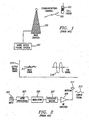
- Fig. 1 is a Prior Art block diagram illustrating a system environment used with example embodiments of the invention.
- a wireless communication device 101 communicates, using a communications channel 103, with a base station 105.
- the base station 105 couples the communications from the wireless communication device into the land based phone system 107.
- the amplitude of the broadcast signal will vary depending on whether the wireless communication device 101 is far from or near to the base station 105. If the device 101 is near to the base station a near signal 217, that is a comparatively low amplitude signal when compared with the output signal Range 215 is generated. If the device 101 is farther from the base station, a far signal 219 is generated. The far signal 219 is of a comparatively higher amplitude signal than the near signal 217. Changing the amplitude of the output signal, depending on the distance of the phone from the base station, is advantageous for several reasons. One reason is that power may be conserved, when the device 101 is relatively near the base station 105.
- wireless communication devices may change their power so that the signal arriving at the base station, from the device, is relatively constant, regardless of the distance of the device is from the base station. Because the transmitted signals are arising at the base station with similar power levels, it is easier for the base station to process the incoming signals.
- a RF power amplifier within a wireless communication device is an analog type amplifier, such as.a class A type amplifier.
- Class A amplifiers typically have a quiescent current, even when no signal is being output.
- Class A amplifiers are commonly known for both inefficiency and linearity. Linearity is often a trade off with power dissipation. This trade off is especially true in the case of the class A amplifiers, that dissipate a significant amount of power, as compared with their output power.
- Another characteristic of class A amplifiers is that they are easily controllable to vary their output.
- Another type of amplifier is a class D amplifier. Class D amplifiers operate by switching between saturation and cutoff. When the amplifier is in a saturation mode, the current in the output of the amplifier is at a maximum.
- the output is saturated, there is little voltage developed at the output. Because of the low voltage across the output, the power dissipated is minimal.
- the output of the amplifier is at a maximum voltage, but the current through the output is a small value, typically a leakage current or zero.
- the class D amplifier typically varies between full on (saturation) and full off (cutoff).
- a waveform such as 313, may be seen at the output 307 of the integrator circuit 303.
- the waveform 313 has a greater amplitude than the waveform 309. Because the changing of the duty cycle of the class D amplifier results in differing amplitude waveforms, when coupled into the integrator 303, the output generated by the amplifier may be changed. If the output of the class D amplifier is coupled into a pulse shaping network containing a resonant circuit, a waveform approaching a sine wave in shape may be generated. Therefore, by modulating the duty cycle of the Class D amplifier, a variable amplitude waveform may be generated.
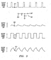
- Waveform 412 is an amplified copy of waveform 408.
- the waveform 412 switches between a minimum value, i.e. saturation of the RF amplifier 410 and a maximum value, i.e. the cutoff of the RF amplifier 410.
- the output of the RF amplifier 410 may be coupled into an RC circuit consisting of the resistor 414 and the capacitor 416.
- the waveform at the junction of 414 and 416 is shown in graph 418.
- the waveform 418 has an excursion, illustratively of about 20% of the difference between its minimum and maximum value.
- the waveform at the junction of 414 and 416 is further coupled into the resonant circuit 420.
- the resonant circuit is tuned to the frequency of the reference frequency 406.
- the output 422 of the resonant circuit 420 is a sine wave with an excursion, illustratively of about 20% of the difference between its minimum and maximum value, as shown in graph 424.
- the output 422 of the output stage RF circuit for the "near" case may be chosen to be adequate in the case where the wireless communication device is near the base station.
- the "far" condition 426 occurs when the wireless communication device, of the illustrated embodiment, is operating relatively far from a base station.
- the duty cycle block 402 receives a control signal 404, signaling that the unit is operating in a "far” condition.
- the duty cycle block 402 adjusts the duty cycle of a reference frequency 406, so that the duty cycle is, illustratively about 40%.
- the duty cycle waveform 428 is the result of the adjustment of the duty cycle of the reference frequency approximately 40%.
- the RF amplifies 410 receives the waveform 428 from the duty cycle block 402 and produces waveform 430.
- Waveform 430 is an amplified copy of waveform 428.
- the waveform 430 switches between a minimum value, i.e. saturation of the RF amplifier 410 and a maximum value, i.e. the cutoff of the RF amplifier 410.
- the output of the RF amplifier 410 is coupled into an RC circuit consisting of the resistor 414 and the capacitor 416.
- the waveform at the junction of 414 and 416 is shown in graph 432.
- the waveform 432 has an excursion of about 40% of the difference between its minimum and maximum value.
- the RF output 422 power may be changed to accommodate both the "near” and “far” cases. Since changing the duty cycle may change the amplitude of the output signal, the duty cycle block 402 may be used to amplitude modulate the output signal. The amplitude modulation of the signal may take place concurrently with the accommodation of the "near" and "far” case as discussed above. For example, in the “near” case, the duty cycle was 20% by using the control signal 404. If the duty cycle of the waveform is varied between 15% and 25%, the "near" signal may be amplitude modulated. In a like manner, in the "far” case, the duty cycle was 40%.
- the "far" signal may be amplitude modulated.
- both the average output power level and the amplitude modulation of then RF signal may be accomplished digitally.
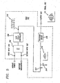
- a digital combination of average power output and amplitude modulation is illustrated in Fig. 5 .
- a signal representative of the desired average power is coupled into a first input 500 and is combined with a signal representing the instantaneous desired amplitude modulation coupled into a second input 502 of the Digital Amplitude Modulating Circuit ("DAMC') 504.
- DAMC' Digital Amplitude Modulating Circuit
- the desired average power signal coupled into the first input 500 is combined in a summation unit 506, with the desired instantaneous amplitude modulation signal coupled into the second input 502.
- the output of the summation unit 506, representing the sum of desired average power and the desired instantaneous amplitude modulation, is coupled into the duty cycle controller 508.
- the resulting signal output from the duty cycle controller 510 represents a signal, the duty cycle of which is dependent on both the average power signal at input 500 and the amplitude modulation signal at input 502.
- the output signal 510 of the duty cycle controller 508 is coupled into an integrating network comprising resistor R 512 and capacitor C 514.
- the output of the integrating network, the junction of R 512 and C 514, is a waveform 516 that contains components representative of both the average power signal 500 and the amplitude modulation signal 502.
- the waveform 516 is then further coupled into a resonant circuit 518.
- the output 520 of the resonant circuit 518 is a modulated RF signal having an average power and amplitude modulation that may be controlled digitally.
- the Digital Amplitude Modulating Circuit ("DAMC') 504 may be a component in a overall digital modulation scheme.
- Phase Shift Keying is a popular method for modulating a carrier signal with a data signal.
- PSK Phase Shift Keying
- the phase of a carrier signal for example a Sine wave
- Fig. 6 illustrates a basic form of phase shift keying commonly known as Binary Phase Shift Keying ("BPSK").
- BPSK Binary Phase Shift Keying
- waveform 600 represents a digital data signal.
- vector 800 represents bit pair 00, a phase shift of 135°, i.e. vector 802, represents bit pair 00, a phase shift of 255°, i.e. vector 804, represents bit pair 11, and a phase shift of 315°, i.e. vector 806, represents bit pair 01.
- These pairs of bits are commonly referred to as dibits or symbols.
- distinct information states of PSK signals are commonly referred to as symbols.
- a symbol may be larger than a dibit and may contain several bits of information.
- the phase of the received signal may be compared to a reference signal.
- This may be accomplished by coupling the received signal into a balanced demodulator and providing a reference signal having a frequency and phase that is approximately identical to the carrier used to modulate the signal. Because of the necessity of providing a signal that has a phase and frequency identical to the carrier signal used in the modulation process, balanced demodulator type circuitry may be complex and expensive. To avoid the requirement of producing a carrier having a frequency and phase that is identical to the carrier used to modulate the signal, differential PSK techniques may be used. In Differential PSK (“DPSK”), there is no absolute phase and, as a result, there is no requirement to provide a carrier with frequency and phase identical to the carrier used to modulate the signal.
- DPSK Differential PSK
- the binary data is recovered from a DPSK signal by comparing the phase of the signal being received to the phase of the previous symbol received. Comparing a symbol to the previous symbol received, avoids the dependency on an absolute reference. It is often convenient to refer to phase modulated signals as vectors in the frequency domain rather than the time domain.
- I/Q diagrams are often employed instead of the traditional time domain representation. I/Q diagrams commonly depict Q as a vertical axis and I as the horizontal axis. The I axis represents the in-phase part of the signal vector and Q axis represents the quadrature portion of the signal vector.
- a signal may be represented as a vector rotating in the I/Q plane with the length of the vector representing the amplitude of the signal.
- a further embodiment of the invention comprises a digital method of phase modulating a signal. Such a method may be used to replace the switching between carriers offset by a given phase, as illustrated in Fig. 7 .
- One embodiment of the digital phase modulator is the sigma delta digital modulator 1000, as illustrated in Fig. 10 .
- the waveform 1010 is also generated by dividing the waveform 1004 by four, using standard digital techniques, except that the second cycle has been delayed by 90° from the first, when compared with waveform 1008.
- the second cycle of waveform 1010 is delayed by 90°, simply by delaying the start of the second cycle of the waveform 1010 by one cycle of the reference frequency 1004.
- the waveform 1012 is also generated by dividing the 1004 waveform by four, using standard digital techniques, except that the second cycle has been delayed by 180°, with respect to the 0° waveform 1008.
- the second cycle of waveform 1012 is delayed by 180° simply by delaying the start of the second cycle of the waveform 1012 by two cycles of the reference frequency 1004.
- the waveform 1014 is also generated by dividing the 1004 waveform by four, using standard digital techniques, except that the second cycle has been delayed by 270° with respect to the 0° waveform 1008.
- the second cycle of waveform 1014 is delayed by 270° simply by delaying the start of the second cycle of the waveform 1014 by three cycles of the reference frequency 1004.
- the Sigma Delta Digital Modulator 1000 may be used to encode QPSK, or any other 4 symbol phase modulation.
- An output 1016, comprising a quadrature encoded signal 1018, may be produced using the just described Delta Sigma Digital Modulator 1000 and standard digital circuitry.
- the PDM 1100 produces an output 1108 that comprises a phase modulated signal 1110, by accepting a reference signal 1104 and coupling it into a series of dividers 1112, 1114, 1116 and 1118.
- Each divider has its own divide ratio different from the other dividers, so the frequencies out of the dividers will all be different.
- the divide ratio at divider 1112 is smallest and increases at dividers 1114, 1116 and 1118, respectively. In other words N ⁇ N + X ⁇ N + Y ⁇ N + Z.
- the signal that is produced by divider 1114 has a period that is 90° longer than divider 1112.
- the signal that is produced by divider 1116 has a period that is 180° longer than divider 1112.
- the signal is produced by of divider 1118 has a period that is 270° longer than divider 1112. This means that the output of 1118 is delayed by 270° with respect to the output of 1112, the output of 1116 is delayed by 180° with respect to the output of 1112, and the output of 1114 is delayed by 90° with respect to the output of 1112.
- the phase information 1102 is used to activate S1-(1120), S2-(1122), S3-(1124), or S4-(1126), depending on whether a phase of 0°, 90°, 180°, or 270° is desired.
- the output acts as a reset 1128 to all the counters within the divider circuits (1112, 1114, 1116, and 1118), and the PDM 1100 is then reset and ready to generate the next pulse.
- the PDM 1100 may be extended to any number of phase delays by changing the reference signal 1104 frequency, adding dividers with the correct divide ratio, and adding selection switches to select between the dividers.
- Figure 12 represents an embodiment of the claimed invention in that a Digital Amplitude Modulating Circuit (“DAMC"), as illustrated in Fig. 4 that is combined with a Delta Sigma Digital Modulator (“DSDM”) or a Programmable Divide Modulator (“PDM”).
- DAMC Digital Amplitude Modulating Circuit
- DSDM Delta Sigma Digital Modulator
- PDM Programmable Divide Modulator
- the connections between the components may be purely digital, analog or mixed.
- the various embodiments may be combined with digital or analog subsystems, depending on the implementation desired.
- summation 1200 depicts two inputs, where an average power signal 1202 is coupled to one input and an amplitude component signal 1204 is coupled to the other input.
- the summation 1200 may be implemented as an operational amplifier summation unit, if the average power signal 1202 and the amplitude component signal 1204 are analog control voltages.
- the summation 1200 may be implemented as a clocked digital adder unit, if the average power signal 1202 and the amplitude component signal 1204 are digital values. The same is true of the other units illustrated in Fig. 12 .
- the choice of analog or digital control of the blocks within the system is one of implementation only, the basic functioning of the digital blocks will remain unchanged.
- a PSK signal 1206 may be decomposed into amplitude and phase components 1208.
- the decomposition 1208 may be the same type as illustrated in Fig. 7 , at block 700. Signal decomposition of PSK signals may be accomplished in a variety of ways, utilizing methods well known in the art.
- An amplitude component signal 1204 representing the amplitude portion of the PSK signal is then coupled into the summation 1200, where it is summed with the average power signal. 1202 to produce a sum signal 1137.
- the average power signal 1202 is representative of the average broadcast power desired.
- the sum signal 1137 is then coupled into a first input of a Digital Amplitude Modulating Circuit ("DAMC").
- the DAMC may be the same as DAMC of Fig. 4 .
- the average power signal 1202 represents the desired output RF power of the system.
- the phase component signal 1212 output from the decomposition 1208 is then used as a control signal for a DSDM 1214 or a PDM 1214.
- the signal from signal generator 1222 would be coupled into an analog to digital converter 1234.
- the output of the analog to digital converter 1234 would then be coupled into register 1236 on the falling clock edge of a signal from the DSDM or PDM 1214.
- the value would then be coupled from register 1236 to register 1238 on the rising edge of a signal from the DSDM or PDM 1214. Since the the DSDM or PDM 1214, provides a signal that has four different periods representing QPSK values between falling and rising edges, the phase of the signal 1228 produced by signal generator 1222 is variably delayed.
- the output of register 1222 may then be converted into an analog value in the digital to analog converter 1240, and then coupled into the amplitude modulation input, such as 502 in Fig.
Landscapes
- Engineering & Computer Science (AREA)
- Computer Networks & Wireless Communication (AREA)
- Signal Processing (AREA)
- Power Engineering (AREA)
- Transmitters (AREA)
- Amplifiers (AREA)
- Digital Transmission Methods That Use Modulated Carrier Waves (AREA)
- Compression, Expansion, Code Conversion, And Decoders (AREA)
- Input Circuits Of Receivers And Coupling Of Receivers And Audio Equipment (AREA)
- Radar Systems Or Details Thereof (AREA)
Claims (14)
- Vorrichtung zur digitalen Erzeugung eines modulierten Funkfrequenzsignals (RF-Signals) von vorgegebener Höhe, bestehend aus:einer Signalzerlegungseinheit (1208) zum Empfang eines Phasenmodulationssignals (PSK-Signals) und zur Zerlegung des PSK-Signals in ein Phasenkomponentensignal (1212) und ein Amplitudenkomponentensignal (1204);eine digitale Phasenmodulationseinheit (1214) zum Empfang des Phasenkomponentensignals und zur Erzeugung eines digitalen phasenmodulierten Signal (1216);einen Signalgeber (1222) zur Lieferung eines periodischen Signals (1220);eine Verzögerungseinheit (1218) mit einem ersten Input zum Empfang des digitalen phasenmodulierten Signals und einen zweiten Input zum Empfang des periodischen Signals und zur Erzeugung einer Verzögerung im periodischen Signal proportional zum digitalen phasenmodulierten Signal, wodurch ein verzögertes periodisches Signal (1228) entsteht, indem die Verzögerung proportional zum digitalen phasenmodulierten Signal ist;eine Summiereinheit (1200) mit einem ersten Input zum Empfang eines Signals von durchschnittlicher Leistung (1202) und mit einem zweiten Input zum Empfang des Amplitudenkomponentensignals (1204), wobei das Signal durchschnittlicher Leistung mit dem Amplitudenkomponentensignal kombiniert ist und wobei ein Summensignal (1137) erzeugt wird; undeine digitale Amplitudenmodulations-Schaltung ["DAMC"] (1230) zum Empfang des verzögerten periodischen Signals und zum Empfang des Summensignals und zur Erzeugung eines modulierten Funkfrequenzsignals (RF-Signals).
- Vorrichtung gemäß Anspruch 1, dadurch gekennzeichnet, dass die digitale Phasenmodulationseinheit einen Delta-Sigma-Digitalmodulator ("DSDM") aufweist.
- Vorrichtung gemäß Anspruch 2, dadurch gekennzeichnet, dass der DSDM so betrieben werden kann, dass er ein Bezugssignal mit einer Frequenz empfängt, die ein vorgegebenes Mehrfaches einer Frequenz des digitalen phasenmodulierten Signals darstellt und dass er das digitale phasenmodulierte Signal als Reaktion auf das Phasenkomponentensignal erzeugt, indem er das Bezugssignal durch das vorgegebene Mehrfache teilt und eine vorgegebene Anzahl an Bezugssignalzyklen verzögert.
- Vorrichtung gemäß Anspruch 2, dadurch gekennzeichnet, dass der DSDM so betrieben werden kann, dass er ein Bezugssignal mit einer Frequenz empfängt, die einem Vierfachen der Frequenz des digitalen phasenmodulierten Signals entspricht, und das digitale phasenmodulierte Signal erzeugt, indem er das Bezugssignal durch vier teilt und als Reaktion auf das Phasenkomponentensignal bis zu drei Bezugssignalzyklen verzögert.
- Vorrichtung gemäß Anspruch 1, dadurch gekennzeichnet, dass die digitale Phasenmodulationseinheit einen programmierbaren Dividiermodulator ("PDM") aufweist.
- Vorrichtung gemäß Anspruch 5, dadurch gekennzeichnet, dass der PDM so betrieben werden kann, dass er ein Referenzsignal empfängt und das digitale phasenmodulierte Signal als Reaktion auf das Phasenkomponentensignal erzeugt, indem er das Bezugssignal durch eine Reihe von Dividierern teilt, die jeweils eine Dividierrate haben, die von den anderen abweicht, und einen Schalter auslöst, um einen Output eines der Dividierer als das digitale phasenmodulierte Signal zu wählen.
- Vorrichtung gemäß Anspruch 5, dadurch gekennzeichnet, dass das digitale phasenmodulierte Signal bewirkt, dass sich die Dividierer auf Null stellen.
- Vorrichtung gemäß Anspruch 1, dadurch gekennzeichnet, dass die Verzögerungseinheit eine digitale Verzögerungseinheit darstellt.
- Vorrichtung gemäß Anspruch 1, dadurch gekennzeichnet, dass die Verzögerungseinheit eine analoge Verzögerungseinheit darstellt.
- Verfahren zur digitalen Erzeugung eines modulierten RF-Signals von vorgegebener Höhe, bestehend aus:Zerlegung eines PSK-Signals in ein Phasenkomponentensignal und ein Amplitudenkomponentensignal;Erzeugung eines digitalen phasenmodulierten Signals aus dem Phasenkomponentensignal;Erzeugung eines periodischen Signals;Erzeugung einer Verzögerung im periodischen Signal proportional zum digitalen phasenmodulierten Signal, wodurch ein verzögertes periodisches Signal erzeugt wird, indem die Verzögerung proportional zum digitalen phasenmodulierten Signal ist;Kombination eines Signals von durchschnittlicher Leistung mit dem Amplitudenkomponentensignal und Erzeugung eines Summensignals; undKopplung des verzögerten periodischen Signals mit dem Summensignal zu einer digitalen Amplitudenmodulations-Schaltung ["DAMC"], wodurch ein moduliertes Funkfrequenzsignal (RF-Signal) erzeugt wird.
- Verfahren gemäß Anspruch 10, dadurch gekennzeichnet, dass der Verfahrensschritt der Erzeugung eines digitalen phasenmodulierten Signals daraus besteht, dass ein Delta-Sigma-Digitalmodulator ("DSDM") eingesetzt wird, um ein digitales phasenmoduliertes Signal zu erzeugen.
- Verfahren gemäß Anspruch 10, dadurch gekennzeichnet, dass der Verfahrensschritt der Erzeugung eines digitalen phasenmodulierten Signals daraus besteht, dass ein programmierbarer Dividiermodulator ("PDM") eingesetzt wird, um ein digitales phasenmoduliertes Signal zu erzeugen.
- Verfahren gemäß Anspruch 10, dadurch gekennzeichnet, dass der Verfahrensschritt der Erzeugung einer Verzögerung in der periodischen Signalverzögerungseinheit daraus besteht, dass ein periodisches Signal mit einer digitalen Verzögerungseinheit verzögert wird.
- Verfahren gemäß Anspruch 10, dadurch gekennzeichnet, dass der Verfahrensschritt der Erzeugung einer Verzögerung in der periodischen Signalverzögerungseinheit daraus besteht, dass ein periodisches Signal mit einer analogen Verzögerungseinheit verzögert wird.
Applications Claiming Priority (2)
| Application Number | Priority Date | Filing Date | Title |
|---|---|---|---|
| US09/814,196 US6754287B2 (en) | 2001-03-21 | 2001-03-21 | Method and apparatus for producing a modulated signal |
| EP02719290A EP1410495B1 (de) | 2001-03-21 | 2002-03-20 | System zur steuerung eines klasse-d-verstärkers |
Related Parent Applications (2)
| Application Number | Title | Priority Date | Filing Date |
|---|---|---|---|
| EP02719290.5 Division | 2002-03-20 | ||
| EP02719290A Division EP1410495B1 (de) | 2001-03-21 | 2002-03-20 | System zur steuerung eines klasse-d-verstärkers |
Publications (3)
| Publication Number | Publication Date |
|---|---|
| EP2019485A2 EP2019485A2 (de) | 2009-01-28 |
| EP2019485A3 EP2019485A3 (de) | 2009-08-05 |
| EP2019485B1 true EP2019485B1 (de) | 2010-10-13 |
Family
ID=25214400
Family Applications (2)
| Application Number | Title | Priority Date | Filing Date |
|---|---|---|---|
| EP02719290A Expired - Lifetime EP1410495B1 (de) | 2001-03-21 | 2002-03-20 | System zur steuerung eines klasse-d-verstärkers |
| EP08017773A Expired - Lifetime EP2019485B1 (de) | 2001-03-21 | 2002-03-20 | Digitaler HF Modulator |
Family Applications Before (1)
| Application Number | Title | Priority Date | Filing Date |
|---|---|---|---|
| EP02719290A Expired - Lifetime EP1410495B1 (de) | 2001-03-21 | 2002-03-20 | System zur steuerung eines klasse-d-verstärkers |
Country Status (7)
| Country | Link |
|---|---|
| US (1) | US6754287B2 (de) |
| EP (2) | EP1410495B1 (de) |
| KR (1) | KR100599148B1 (de) |
| CN (1) | CN100341241C (de) |
| AT (2) | ATE484880T1 (de) |
| DE (2) | DE60232333D1 (de) |
| WO (1) | WO2002078170A1 (de) |
Families Citing this family (19)
| Publication number | Priority date | Publication date | Assignee | Title |
|---|---|---|---|---|
| US7876855B2 (en) * | 2001-08-28 | 2011-01-25 | Northrop Grumman Systems Corporation | Phase modulation power spreading used to reduce RF or microwave transmitter output power spur levels |
| US20030123566A1 (en) * | 2001-12-27 | 2003-07-03 | Jaime Hasson | Transmitter having a sigma-delta modulator with a non-uniform polar quantizer and methods thereof |
| US7336753B2 (en) * | 2003-06-26 | 2008-02-26 | Marvell International Ltd. | Transmitter |
| US20050041706A1 (en) * | 2003-08-20 | 2005-02-24 | Vikram Magoon | Laser driver circuit |
| US7912145B2 (en) * | 2003-12-15 | 2011-03-22 | Marvell World Trade Ltd. | Filter for a modulator and methods thereof |
| US7356315B2 (en) * | 2003-12-17 | 2008-04-08 | Intel Corporation | Outphasing modulators and methods of outphasing modulation |
| US7649958B2 (en) * | 2004-06-25 | 2010-01-19 | Sige Semiconductor (Europe) Limited | Transmit signal generator and method |
| US8355465B2 (en) * | 2004-11-10 | 2013-01-15 | Sige Semiconductor (Europe) Limited | Driver circuit for driving a power amplifier |
| US7471154B2 (en) | 2006-08-08 | 2008-12-30 | Skyworks Solutions, Inc. | Bias circuit for maintaining high linearity at cutback power conditions |
| US7446612B2 (en) | 2006-09-08 | 2008-11-04 | Skyworks Solutions, Inc. | Amplifier feedback and bias configuration |
| US7719141B2 (en) * | 2006-11-16 | 2010-05-18 | Star Rf, Inc. | Electronic switch network |
| US7696826B2 (en) | 2006-12-04 | 2010-04-13 | Skyworks Solutions, Inc. | Temperature compensation of collector-voltage control RF amplifiers |
| WO2009001233A1 (en) * | 2007-06-26 | 2008-12-31 | Nxp B.V. | Power-efficient transmitter for magnetic link |
| US8509346B2 (en) * | 2007-10-10 | 2013-08-13 | St-Ericsson Sa | Transmitter with reduced power consumption and increased linearity and dynamic range |
| EP2301147A2 (de) * | 2008-06-16 | 2011-03-30 | Universite Aix-Marseille I | Klasse-d-digitalverstärker mit einem rauschminderer |
| US20100019857A1 (en) * | 2008-07-22 | 2010-01-28 | Star Rf, Inc. | Hybrid impedance matching |
| CN108233875B (zh) * | 2016-12-13 | 2021-07-06 | 台达电子工业股份有限公司 | 射频放大器及提高其效率的方法、以及射频电源供应器 |
| WO2018183189A1 (en) * | 2017-03-27 | 2018-10-04 | Waveguide Corporation | Integrated switched-mode power amplifiers |
| US12231129B2 (en) * | 2022-04-26 | 2025-02-18 | Changxin Memory Technologies, Inc. | Signal generator and memory |
Family Cites Families (17)
| Publication number | Priority date | Publication date | Assignee | Title |
|---|---|---|---|---|
| US4584541A (en) * | 1984-12-28 | 1986-04-22 | Rca Corporation | Digital modulator with variations of phase and amplitude modulation |
| JPH0289440A (ja) * | 1988-09-27 | 1990-03-29 | Victor Co Of Japan Ltd | ディジタル4相psk変調器 |
| JPH0646032A (ja) * | 1991-10-24 | 1994-02-18 | Ricoh Co Ltd | スペクトル拡散通信方式 |
| JP3419484B2 (ja) * | 1992-03-30 | 2003-06-23 | 株式会社東芝 | 変調器、送信器 |
| US5450044A (en) | 1993-04-14 | 1995-09-12 | Acrodyne Industries, Inc. | Quadrature amplitude modulator including a digital amplitude modulator as a component thereof |
| US5627499A (en) * | 1995-10-13 | 1997-05-06 | Pacific Communication Sciences, Inc. | Digital modulator and upconverter having single-bit delta-sigma data converters |
| US5859869A (en) * | 1995-11-17 | 1999-01-12 | Sanconix, Inc. | Low cost binary phase shift keying modulation transmitter system |
| US5705959A (en) * | 1996-10-08 | 1998-01-06 | The United States Of America As Represented By The Secretary Of The Air Force | High efficiency low distortion amplification |
| US5838210A (en) * | 1997-12-01 | 1998-11-17 | Motorola, Inc. | Method and apparatus for generating a modulated signal |
| US5942938A (en) * | 1997-12-29 | 1999-08-24 | Motorola, Inc. | Method and apparatus for high efficiency power amplification |
| US6101224A (en) | 1998-10-07 | 2000-08-08 | Telefonaktiebolaget Lm Ericsson | Method and apparatus for generating a linearly modulated signal using polar modulation |
| FI105609B (fi) * | 1998-10-27 | 2000-09-15 | Nokia Mobile Phones Ltd | Menetelmä ja järjestely lähetyssignaalin muodostamiseksi |
| US6194963B1 (en) | 1998-11-18 | 2001-02-27 | Ericsson Inc. | Circuit and method for I/Q modulation with independent, high efficiency amplitude modulation |
| EP1035701A1 (de) * | 1999-03-08 | 2000-09-13 | Motorola, Inc. | Modulator, der Einhüllendenbeseitigung und -Wiederherstellung mittels Nachschlagtabellen verwendet |
| JP2000286915A (ja) * | 1999-03-31 | 2000-10-13 | Toshiba Corp | 信号変調回路及び信号変調方法 |
| US6369648B1 (en) * | 1999-04-21 | 2002-04-09 | Hughes Electronics Corporation | Linear traveling wave tube amplifier utilizing input drive limiter for optimization |
| EP1197051A1 (de) * | 1999-07-21 | 2002-04-17 | Siemens Aktiengesellschaft | Modulationsschaltung zur erzeugung eines zugleich phasen- und amplitudenmodulierten signals |
-
2001
- 2001-03-21 US US09/814,196 patent/US6754287B2/en not_active Expired - Lifetime
-
2002
- 2002-03-20 EP EP02719290A patent/EP1410495B1/de not_active Expired - Lifetime
- 2002-03-20 CN CNB028068521A patent/CN100341241C/zh not_active Expired - Lifetime
- 2002-03-20 DE DE60232333T patent/DE60232333D1/de not_active Expired - Lifetime
- 2002-03-20 DE DE60238008T patent/DE60238008D1/de not_active Expired - Lifetime
- 2002-03-20 AT AT08017773T patent/ATE484880T1/de not_active IP Right Cessation
- 2002-03-20 KR KR1020037012329A patent/KR100599148B1/ko not_active Expired - Lifetime
- 2002-03-20 AT AT02719290T patent/ATE431644T1/de not_active IP Right Cessation
- 2002-03-20 EP EP08017773A patent/EP2019485B1/de not_active Expired - Lifetime
- 2002-03-20 WO PCT/US2002/008550 patent/WO2002078170A1/en not_active Ceased
Also Published As
| Publication number | Publication date |
|---|---|
| EP1410495B1 (de) | 2009-05-13 |
| CN1518792A (zh) | 2004-08-04 |
| ATE484880T1 (de) | 2010-10-15 |
| EP2019485A2 (de) | 2009-01-28 |
| WO2002078170A1 (en) | 2002-10-03 |
| EP1410495A1 (de) | 2004-04-21 |
| CN100341241C (zh) | 2007-10-03 |
| KR20040015070A (ko) | 2004-02-18 |
| EP1410495A4 (de) | 2004-10-06 |
| ATE431644T1 (de) | 2009-05-15 |
| DE60232333D1 (de) | 2009-06-25 |
| US6754287B2 (en) | 2004-06-22 |
| DE60238008D1 (de) | 2010-11-25 |
| EP2019485A3 (de) | 2009-08-05 |
| KR100599148B1 (ko) | 2006-07-12 |
| US20020136326A1 (en) | 2002-09-26 |
Similar Documents
| Publication | Publication Date | Title |
|---|---|---|
| EP2019485B1 (de) | Digitaler HF Modulator | |
| EP2515444B1 (de) | HF-Sender und Verfahren dafür | |
| US9647866B2 (en) | RF transmitter, integrated circuit device, wireless communication unit and method therefor | |
| US6560296B1 (en) | Method and apparatus for modulating digital data | |
| WO2015040773A1 (ja) | 送信機及びその制御方法 | |
| US20060115005A1 (en) | Direct conversion delta-sigma transmitter | |
| US6940920B2 (en) | Multiplier arrangement, signal modulator and transmitter | |
| US7474708B1 (en) | Multimode transmitter architecture | |
| JP4817890B2 (ja) | 増幅装置、ポーラ変調送信装置及び無線通信装置 | |
| WO2012166281A1 (en) | Method and apparatus of switched amplification having improved efficiency | |
| AU2020274536B2 (en) | Programmable polar and cartesian radio frequency digital to analog converter | |
| JP6755093B2 (ja) | 無線送信装置及び無線送信方法 | |
| US7812684B2 (en) | Communication apparatus | |
| JP6950043B2 (ja) | 無線送信装置及び無線送信方法 | |
| Zhang et al. | CORDIC-Less Digital Polar Transmitter Architecture Based on Delta-Sigma Modulator | |
| LaRue | A Fully-Integrated Four-way Outphasing Architecture in Heterogeneously Integrated CMOS/GaN Process Technologies | |
| KR0153011B1 (ko) | 변조기 | |
| EP3499728A1 (de) | Digitale leistungsverstärkungsschaltung | |
| Nuyts et al. | Digital Transmitter Architectures: Overview | |
| Prasanna et al. | UNIVERSAL PROGRAMMABLE MODULATOR ARCHITECTURE FOR SOFTWARE DEFINED RADIO | |
| MXPA00012487A (en) | Digital phase modulator using non-linear amplifiers and a ring oscillator |
Legal Events
| Date | Code | Title | Description |
|---|---|---|---|
| PUAI | Public reference made under article 153(3) epc to a published international application that has entered the european phase |
Free format text: ORIGINAL CODE: 0009012 |
|
| AC | Divisional application: reference to earlier application |
Ref document number: 1410495 Country of ref document: EP Kind code of ref document: P |
|
| AK | Designated contracting states |
Kind code of ref document: A2 Designated state(s): AT BE CH CY DE DK ES FI FR GB GR IE IT LI LU MC NL PT SE TR |
|
| PUAL | Search report despatched |
Free format text: ORIGINAL CODE: 0009013 |
|
| AK | Designated contracting states |
Kind code of ref document: A3 Designated state(s): AT BE CH CY DE DK ES FI FR GB GR IE IT LI LU MC NL PT SE TR |
|
| 17P | Request for examination filed |
Effective date: 20100126 |
|
| GRAP | Despatch of communication of intention to grant a patent |
Free format text: ORIGINAL CODE: EPIDOSNIGR1 |
|
| RTI1 | Title (correction) |
Free format text: DIGITAL RF MODULATOR |
|
| AKX | Designation fees paid |
Designated state(s): AT BE CH CY DE DK ES FI FR GB GR IE IT LI LU MC NL PT SE TR |
|
| GRAS | Grant fee paid |
Free format text: ORIGINAL CODE: EPIDOSNIGR3 |
|
| GRAA | (expected) grant |
Free format text: ORIGINAL CODE: 0009210 |
|
| AC | Divisional application: reference to earlier application |
Ref document number: 1410495 Country of ref document: EP Kind code of ref document: P |
|
| AK | Designated contracting states |
Kind code of ref document: B1 Designated state(s): AT BE CH CY DE DK ES FI FR GB GR IE IT LI LU MC NL PT SE TR |
|
| REG | Reference to a national code |
Ref country code: GB Ref legal event code: FG4D |
|
| REG | Reference to a national code |
Ref country code: CH Ref legal event code: EP |
|
| REG | Reference to a national code |
Ref country code: IE Ref legal event code: FG4D |
|
| REF | Corresponds to: |
Ref document number: 60238008 Country of ref document: DE Date of ref document: 20101125 Kind code of ref document: P |
|
| REG | Reference to a national code |
Ref country code: NL Ref legal event code: VDEP Effective date: 20101013 |
|
| PG25 | Lapsed in a contracting state [announced via postgrant information from national office to epo] |
Ref country code: FI Free format text: LAPSE BECAUSE OF FAILURE TO SUBMIT A TRANSLATION OF THE DESCRIPTION OR TO PAY THE FEE WITHIN THE PRESCRIBED TIME-LIMIT Effective date: 20101013 Ref country code: PT Free format text: LAPSE BECAUSE OF FAILURE TO SUBMIT A TRANSLATION OF THE DESCRIPTION OR TO PAY THE FEE WITHIN THE PRESCRIBED TIME-LIMIT Effective date: 20110214 Ref country code: NL Free format text: LAPSE BECAUSE OF FAILURE TO SUBMIT A TRANSLATION OF THE DESCRIPTION OR TO PAY THE FEE WITHIN THE PRESCRIBED TIME-LIMIT Effective date: 20101013 Ref country code: SE Free format text: LAPSE BECAUSE OF FAILURE TO SUBMIT A TRANSLATION OF THE DESCRIPTION OR TO PAY THE FEE WITHIN THE PRESCRIBED TIME-LIMIT Effective date: 20101013 Ref country code: AT Free format text: LAPSE BECAUSE OF FAILURE TO SUBMIT A TRANSLATION OF THE DESCRIPTION OR TO PAY THE FEE WITHIN THE PRESCRIBED TIME-LIMIT Effective date: 20101013 |
|
| PG25 | Lapsed in a contracting state [announced via postgrant information from national office to epo] |
Ref country code: GR Free format text: LAPSE BECAUSE OF FAILURE TO SUBMIT A TRANSLATION OF THE DESCRIPTION OR TO PAY THE FEE WITHIN THE PRESCRIBED TIME-LIMIT Effective date: 20110114 Ref country code: BE Free format text: LAPSE BECAUSE OF FAILURE TO SUBMIT A TRANSLATION OF THE DESCRIPTION OR TO PAY THE FEE WITHIN THE PRESCRIBED TIME-LIMIT Effective date: 20101013 |
|
| PG25 | Lapsed in a contracting state [announced via postgrant information from national office to epo] |
Ref country code: ES Free format text: LAPSE BECAUSE OF FAILURE TO SUBMIT A TRANSLATION OF THE DESCRIPTION OR TO PAY THE FEE WITHIN THE PRESCRIBED TIME-LIMIT Effective date: 20110124 |
|
| PLBE | No opposition filed within time limit |
Free format text: ORIGINAL CODE: 0009261 |
|
| STAA | Information on the status of an ep patent application or granted ep patent |
Free format text: STATUS: NO OPPOSITION FILED WITHIN TIME LIMIT |
|
| PG25 | Lapsed in a contracting state [announced via postgrant information from national office to epo] |
Ref country code: DK Free format text: LAPSE BECAUSE OF FAILURE TO SUBMIT A TRANSLATION OF THE DESCRIPTION OR TO PAY THE FEE WITHIN THE PRESCRIBED TIME-LIMIT Effective date: 20101013 |
|
| 26N | No opposition filed |
Effective date: 20110714 |
|
| PG25 | Lapsed in a contracting state [announced via postgrant information from national office to epo] |
Ref country code: MC Free format text: LAPSE BECAUSE OF NON-PAYMENT OF DUE FEES Effective date: 20110331 |
|
| REG | Reference to a national code |
Ref country code: CH Ref legal event code: PL |
|
| REG | Reference to a national code |
Ref country code: DE Ref legal event code: R097 Ref document number: 60238008 Country of ref document: DE Effective date: 20110714 |
|
| PG25 | Lapsed in a contracting state [announced via postgrant information from national office to epo] |
Ref country code: IT Free format text: LAPSE BECAUSE OF FAILURE TO SUBMIT A TRANSLATION OF THE DESCRIPTION OR TO PAY THE FEE WITHIN THE PRESCRIBED TIME-LIMIT Effective date: 20101013 |
|
| REG | Reference to a national code |
Ref country code: IE Ref legal event code: MM4A |
|
| PG25 | Lapsed in a contracting state [announced via postgrant information from national office to epo] |
Ref country code: CH Free format text: LAPSE BECAUSE OF NON-PAYMENT OF DUE FEES Effective date: 20110331 Ref country code: IE Free format text: LAPSE BECAUSE OF NON-PAYMENT OF DUE FEES Effective date: 20110320 Ref country code: LI Free format text: LAPSE BECAUSE OF NON-PAYMENT OF DUE FEES Effective date: 20110331 |
|
| PG25 | Lapsed in a contracting state [announced via postgrant information from national office to epo] |
Ref country code: LU Free format text: LAPSE BECAUSE OF NON-PAYMENT OF DUE FEES Effective date: 20110320 Ref country code: CY Free format text: LAPSE BECAUSE OF FAILURE TO SUBMIT A TRANSLATION OF THE DESCRIPTION OR TO PAY THE FEE WITHIN THE PRESCRIBED TIME-LIMIT Effective date: 20101013 |
|
| PG25 | Lapsed in a contracting state [announced via postgrant information from national office to epo] |
Ref country code: TR Free format text: LAPSE BECAUSE OF FAILURE TO SUBMIT A TRANSLATION OF THE DESCRIPTION OR TO PAY THE FEE WITHIN THE PRESCRIBED TIME-LIMIT Effective date: 20101013 |
|
| REG | Reference to a national code |
Ref country code: FR Ref legal event code: PLFP Year of fee payment: 15 |
|
| REG | Reference to a national code |
Ref country code: DE Ref legal event code: R082 Ref document number: 60238008 Country of ref document: DE Representative=s name: ISARPATENT - PATENT- UND RECHTSANWAELTE BEHNIS, DE Ref country code: DE Ref legal event code: R082 Ref document number: 60238008 Country of ref document: DE Representative=s name: ISARPATENT - PATENT- UND RECHTSANWAELTE BARTH , DE Ref country code: DE Ref legal event code: R082 Ref document number: 60238008 Country of ref document: DE Representative=s name: ISARPATENT - PATENTANWAELTE- UND RECHTSANWAELT, DE |
|
| REG | Reference to a national code |
Ref country code: FR Ref legal event code: PLFP Year of fee payment: 16 |
|
| REG | Reference to a national code |
Ref country code: FR Ref legal event code: PLFP Year of fee payment: 17 |
|
| PGFP | Annual fee paid to national office [announced via postgrant information from national office to epo] |
Ref country code: FR Payment date: 20210325 Year of fee payment: 20 |
|
| PGFP | Annual fee paid to national office [announced via postgrant information from national office to epo] |
Ref country code: GB Payment date: 20210329 Year of fee payment: 20 Ref country code: DE Payment date: 20210329 Year of fee payment: 20 |
|
| REG | Reference to a national code |
Ref country code: DE Ref legal event code: R071 Ref document number: 60238008 Country of ref document: DE |
|
| REG | Reference to a national code |
Ref country code: GB Ref legal event code: PE20 Expiry date: 20220319 |
|
| PG25 | Lapsed in a contracting state [announced via postgrant information from national office to epo] |
Ref country code: GB Free format text: LAPSE BECAUSE OF EXPIRATION OF PROTECTION Effective date: 20220319 |