EP2018530B1 - A measuring device including a layer of a magnetoelastic alloy and a method for production thereof - Google Patents
A measuring device including a layer of a magnetoelastic alloy and a method for production thereof Download PDFInfo
- Publication number
- EP2018530B1 EP2018530B1 EP07709481.1A EP07709481A EP2018530B1 EP 2018530 B1 EP2018530 B1 EP 2018530B1 EP 07709481 A EP07709481 A EP 07709481A EP 2018530 B1 EP2018530 B1 EP 2018530B1
- Authority
- EP
- European Patent Office
- Prior art keywords
- layer
- less
- range
- alloy
- load
- Prior art date
- Legal status (The legal status is an assumption and is not a legal conclusion. Google has not performed a legal analysis and makes no representation as to the accuracy of the status listed.)
- Active
Links
Images


Classifications
-
- H—ELECTRICITY
- H10—SEMICONDUCTOR DEVICES; ELECTRIC SOLID-STATE DEVICES NOT OTHERWISE PROVIDED FOR
- H10N—ELECTRIC SOLID-STATE DEVICES NOT OTHERWISE PROVIDED FOR
- H10N35/00—Magnetostrictive devices
- H10N35/101—Magnetostrictive devices with mechanical input and electrical output, e.g. generators, sensors
-
- G—PHYSICS
- G01—MEASURING; TESTING
- G01L—MEASURING FORCE, STRESS, TORQUE, WORK, MECHANICAL POWER, MECHANICAL EFFICIENCY, OR FLUID PRESSURE
- G01L3/00—Measuring torque, work, mechanical power, or mechanical efficiency, in general
- G01L3/02—Rotary-transmission dynamometers
- G01L3/04—Rotary-transmission dynamometers wherein the torque-transmitting element comprises a torsionally-flexible shaft
- G01L3/10—Rotary-transmission dynamometers wherein the torque-transmitting element comprises a torsionally-flexible shaft involving electric or magnetic means for indicating
- G01L3/101—Rotary-transmission dynamometers wherein the torque-transmitting element comprises a torsionally-flexible shaft involving electric or magnetic means for indicating involving magnetic or electromagnetic means
- G01L3/102—Rotary-transmission dynamometers wherein the torque-transmitting element comprises a torsionally-flexible shaft involving electric or magnetic means for indicating involving magnetic or electromagnetic means involving magnetostrictive means
- G01L3/103—Details about the magnetic material used
-
- H—ELECTRICITY
- H10—SEMICONDUCTOR DEVICES; ELECTRIC SOLID-STATE DEVICES NOT OTHERWISE PROVIDED FOR
- H10N—ELECTRIC SOLID-STATE DEVICES NOT OTHERWISE PROVIDED FOR
- H10N35/00—Magnetostrictive devices
- H10N35/01—Manufacture or treatment
Definitions
- the present invention relates to a measuring device including a layer of a magnetoelastic alloy formed on a load-carrying member, which layer is intended for measuring stresses induced by a force applied to the load-carrying member, and a method for production thereof.
- the force applied to the load-carrying member is, for example, a tensile force, a compressive force, or a torque.
- the method according to the invention is useful for all types of measuring devices having a measuring layer on a load-carrying member.
- the measuring device measures stresses and/or strain in the layer, for example, induced by tensile forces, compressive forces, and torque applied to the load-carrying member.
- a measuring device according to the present invention may be used as a separate component in all such applications where for different reasons it is of interest to measure forces on a load-carrying member.
- the measuring device may, for example, be used to measure forces in, but not limited to, engines, cars, airplanes, jet engines, bicycles, gear boxes, power steering in cars, tools, propeller engines or helicopters.
- Torque sensors of the type having a stress-measuring magnetoelastic or magnetostrictive layer formed on the surface of a load-carrying member, for example a shaft are well known in the art.
- the purpose of the load-carrying member is to transfer load to the stress-measuring layer.
- a magnetoelastic material is a material that changes its permeability when it is loaded by a force. Examples of magnetoelastic materials are iron, nickel, cobalt and rare earth metals or alloys thereof. In this application the terms magnetoelastic and magnetostrictive are used synonymously.
- the magnetoelastic layer is formed on the surface of the member by different methods, for example by plating, thermal spraying, metal spraying, gun coating, welding, or gluing.
- WO0144770 shows an example of a magnetostrictive sensor for measuring torque in a shaft, wherein the sensor comprises at least one active magnetostrictive region of the shaft.
- the magnetostrictive region includes one or more layers of a magnetostrictive material.
- the application of the layer is performed by plating.
- the plating may be followed by a stabilizing heat treatment at between 150°C and 300°C. In certain applications a higher temperature may also be considered.
- This patent application refers to magnetostrictive material such as pure nickel, where a heating above 300°C would lead to an increased linearity deviation as a consequence. Therefore, heating above 300°C should be avoided for this type of sensor.
- US 5,142,227 describes a method and apparatus for measuring strain in a substrate by attaching thereto a magnetic circuit comprising a ferromagnetic element and sensing a change in the coercive field of the element caused by strain therewith.
- the object of the present invention is to provide a method for producing a layer on a load-carrying member, which makes it possible to manufacture an improved device for measuring stresses induced in the layer, with respect to one or more of the above-mentioned desires and without significantly altering important properties of the load carrying member.
- Such a method comprises: forming a nanocrystalline layer of a magnetoelastic alloy having an average grain size less than 50nm on a surface of a member, and heat treating the layer until a crystallization of the alloy occurs and the average grain size becomes in the range of 100nm to 10 000nm.
- the energy density of magnetoelastic interaction with external stress is proportional to the energy density of magnetic interaction with an external magnetic field. This proportionality depends on magnetic properties such as saturation magnetic induction, saturation magnetostriction, the magnetizing field, stress, and furthermore the size of the magnetic domains.
- the magnetic domain size is proportional to the permeability.
- To design a material with a moderate permeability a small domain size must be achieved. One way to obtain this is to tailor a microstructure of the material with a grain size large enough to accommodate a single domain, but small enough to accommodate just one, or a few. The smallest grain size when this occurs is in the order of fractions of micrometers.
- a nanocrystalline layer having an average grain size less than 50nm provides favorable conditions for crystallization and tailoring the mentioned microstructure.
- the average grain size of said layer is in the range of 100 nm to 5000nm, preferably 100 nm to 1000nm, most preferably 200 nm to 500nm.
- the layer is heat-treated to a temperature above 300°C but less than the melting point of the layer, preferably to a temperature in the range of 350°C to 1000°C, most preferably to a temperature in the range of to 400°C to 800°C.
- the layer In order to achieve the desired crystallization, the layer must be heat-treated to a temperature above the crystallization temperature of the alloy.
- the temperature of the heat-treatment depends on the composition of the alloy. For example, for Ni-Fe-compositions of interest the crystallization temperature is in the range of 350°C-450°C, and thus the temperature of the heat treatment must exceed this temperature. If the layer is heat-treated to a temperature in the range of 400°C to 800°C, the preferred grain structure is easier to obtain.
- the alloy includes iron in the range of 23 - 65 wt% (percent by weight), preferably 30 - 60 wt%, and most preferably 35 - 55 wt%. It has been proven that heat treatment of alloys, including iron in the range of 23 - 65 wt%, to a temperature above 350°C reduces the linearity deviation of the layer and thereby improves its measuring properties. Heat treatment of alloys, including iron in the range of 30 - 60 wt%, to a temperature above 350°C further reduces the linearity deviation and further improves the measuring properties of the alloy.
- Tests have shown that heat treatment of alloys, including less than 20 wt% iron, to a temperature above 350°C has the opposite effect, i.e. the linearity deviation increases, which results in worse measuring properties.
- the resistance against mechanical and thermal fatigue requires thermodynamic stability and stable magnetic properties.
- the Ni-Fe-alloy system presents these properties in the alloying range between 23% and 65%Fe.
- the thermodynamic stability is insufficient for high service temperatures, furthermore, around 20%-23%Fe properties like the magnetostriction and crystal anisotropy change sign and display a strong dependency on chemical composition and methods of manufacturing.
- Above 65%Fe in Ni the Invar alloy range is approached with unsuitable magnetoelastic properties for the objective of this invention.
- the alloy further includes nickel in the range of 35 - 77 wt%, preferably 40 - 70 wt%, and most preferably 45 - 65 wt%.
- nickel in the range of 35 - 77 wt%, preferably 40 - 70 wt%, and most preferably 45 - 65 wt%.
- a particularly advantageous Ni-Fe structure is formed, which has an average grain size within the desired interval and desired magnetic domains.
- This Ni-Fe structure has particularly advantageous magnetoelastic properties and thus improved measuring properties.
- the alloy includes less than 10 wt% of one or more other alloying elements.
- the other alloying elements are for example cobalt, silicon, boron, sulphur, carbon, oxygen, nitrogen, aluminum, germanium, titanium, molybdenum, niobium, silver and copper.
- the alloy is allowed to include less than 10 wt% of other alloying elements in order to achieve the improved measuring properties.
- the layer is heat-treated for a period of time less than 30 seconds.
- the heating time is not critical as long as the requirements on relative permeability and differential permeability are fulfilled. As soon as the crystallization has occurred the heating can be finished.
- the heat treatment should preferably be as fast as possible in order to avoid heating of the load-carrying member and thereby deteriorate its properties, such as the hardening of the member. It is advantageous to use induction heating for the heat treatment since it is fast and provides a local heating of the layer.
- said layer is formed on the member by means of electroplating.
- Electroplating is a suitable method in order to achieve a nanocrystalline layer of the desired grain size.
- the layer is heat-treated until a crystallization of the alloy occurs and the relative permeability becomes less than 500 and the maximum differential permeability becomes less than twice the relative permeability, both measured in a magnetizing field with an amplitude less than 1500 A/m.
- the magnetization curve is essentially straight, which means that saturation of the magnetic induction does not occur. This is advantageous as a sensor with such a layer has an essentially linear output signal as a function of the load.
- Another object of the present invention is to provide a measuring device including a layer of a magnetoelastic alloy formed on a load-carrying member, which device is improved with respect to one or more of the above-mentioned desires.
- Such a measuring device is essentially linear over a large load range, has a low hysteresis, and has an improved stability against ageing and fatigue.
- the invention is particularly useful for producing a sensor for measuring the torque of an engine or transmission, such as the engine or transmission of a car, as the torque sensor produced is linear in the desired load range for such an application.
- Figure 1 shows an example of a measuring device including a load-carrying member, in the form of a rotary shaft 1, which is arranged to transmit a torque in any kind of mechanical transmission.
- the device is adapted to measure torques applied to the load-carrying member.
- the load-carrying member is made of a material with sufficient stiffness, for example of steel.
- a magnetoelastic region 2 is provided on the shaft 1.
- the magnetoelastic region 2 comprises a first layer 3 of a magnetoelastic material, which has a substantially continuous extension and thickness in said region 2.
- the magnetoelastic layer 3 is formed by plating and is mainly composed of iron and nickel.
- a second layer 4 in the form of a continuous strip is provided on the first layer 3.
- the second layer 4 forms a surface pattern on the first layer 3.
- the measuring device includes windings 5a-b supplying the measuring device with an alternating magnetization field. This type of measuring device is, for example, described in more details in the international patent application WO01/44770 .
- the present invention relates to the first magnetoelastic layer 3 and to a method for producing such a layer.
- Differential relative permeability, ⁇ diff 1 ⁇ 0 ⁇ dB dH
- Maximum ⁇ diff is the largest differential relative permeability along the magnetization curve.
- ⁇ is the maximum magnetizing field B is the magnetic induction at H ⁇ 0 is the free space permeability
- Hc the coercive force
- B the reverse magnetizing field needed to restore magnetic induction, B, to zero after saturation magnetization.
- V f ic is the volume fraction of the intercrystalline matter
- a layer with improved measuring properties is achieved if the following conditions are fulfilled for measurements of a magnetic induction curve for the unloaded layer: 1000 > 2 ⁇ ⁇ r > ⁇ diff : H ⁇ ⁇ 1500 ⁇ A m
- the requirement on ⁇ r is that ⁇ r ⁇ 500 and the requirement on ⁇ diff is that ⁇ diff ⁇ 2 ⁇ r measured for a maximum magnetizing field less than 1500A/m.
- the magnetization curve is essentially straight, which means that saturation of the magnetic induction does not occur. This is advantageous as it is makes it possible to produce a sensor with such a layer, which sensor has a linear output signal as a function of the load.
- a method for forming the magnetoelastic layer 3 on the member 1 will be described.
- a nanocrystalline layer of a magnetoelastic alloy having an average grain size less than 50nm is formed on the surface of the load-carrying member 1.
- An average grain size less than 50nm is advantageous as it causes fast growth of the grains during the next step of the method. If the grain size is too large, the desired crystallization will not take place.
- the layer should have an isotropic texture and isomorph grain structure as this represents a good starting point for the desired crystallization.
- the forming is made by means of electroplating.
- other methods such as PVD (Physical Vapor Deposition) methods, CVD (Chemical Vapor Deposition) methods, metal spraying, detonation gun, welding, and gluing.
- the thickness of the layer is typically in the range of 10-500 ⁇ m.
- the average grain size of such a layer is less than 50nm and for example between 10nm and 15nm.
- the magnetoelastic layer is, for example, composed of approximately 40 wt% of iron, approximately 60 wt% of nickel and less than 1 wt% of other alloying elements.
- the layer formed by the plating is either nanocrystalline or amorphous, which is a metastable crystalline state.
- the layer is hard. High internal stress can occur in the layer.
- the mechanical and magnetic properties of the layer are changing.
- the mechanical and magnetic properties also change when the layer is exposed to a repeated mechanical tension. This inclination to change the properties over the lifetime of the device is a bad quality for a sensor.
- Figure 2 shows magnetization curves, i.e. the BH curve, for three different loads on the magnetoelastic layer, measured after the layer has been formed on the member and before it has been heat-treated.
- the curve with a thin continuous line represents -100MPa compressive stress.
- the dashed line represents +100MPa tensile stress.
- the thick continuous line represents an unloaded 0MPa layer.
- Magnetic induction saturation occurs when the BH curve is curved. As seen from the curves, magnetic induction saturation occurs already at zero load. For the zero load curve ⁇ r is about 800 and maximum ⁇ diff is about 5100. Thus, maximum ⁇ diff ⁇ 6.4 ⁇ r .
- the magnetization curves are curved and do not fulfill the requirement on ⁇ r and ⁇ diff.
- a disadvantage with having such a layer in a force measuring sensor is that the output signal becomes non-linear for large loads. Another disadvantage is that a sensor with this layer is not stable over long time due to poor resistance against mechanical and thermal
- the layer is heat-treated to a temperature in the range of 350°C to 1000°C. It is enough to heat the layer until a crystallization of the alloy occurs. Typically, for an iron, nickel alloy this crystallization occurs when the layer reaches a temperature between 350 and 450°C. However, it is possible to heat the layer to a higher temperature and achieve the same type of crystallization, as long as the temperature is essentially below the melting temperature of the alloy. The desired crystallization occurs as soon as the alloy reaches the crystallization temperature. Further heating of the alloy only has a minor effect on the measuring properties. Thus, the time for the heat treatment is fast, less than 30 seconds and typically a few seconds, is enough to achieve the desired crystallization.
- the heating of the layer is for example made by means of induction heating.
- induction heating is that it is fast and concentrates the heating to the magnetoelastic layer, and thus avoids heating the load-carrying member.
- Other possible methods for heating the layer are for example, but not limited to, laser heating, oven heating, and infrared radiation heating.
- the increase of the average grain size is about ten times the size before the crystallization. After crystallization, the average grain size becomes in the range of 100nm to 1000nm, preferably in the range of 200-500nm. The mechanical and magnetic properties after the crystallization become more stable over time and also more stable when exposed to an increased temperature.
- the structure of the electroplated material is usually nanocrystalline.
- Magnetic domain structure of magnetic nanocrystalline and amorphous materials are characterized by large domains, at least tenths of ⁇ m in one direction.
- Nanocrystalline materials are created under thermodynamically non-equilibrium conditions; hence they are in a thermodynamically metastable state.
- the order of the lattice and reducing volume of the intercrystalline matter, i.e. increasing size of crystallites reduces energy and hence makes the system more stable.
- Ni-Fe nanocrystalline material is crystallizing upon heating and forming polycrystalline material with an average grain size equal or exceeding 100nm.
- the crystallization temperature and character in Ni-Fe alloys is dependent on iron concentration, but to our knowledge the onset of crystallization does not exceed 450°C at Ni-Fe concentrations of interest.
- the magnetic domain structure of nanocrystalline or amorphous material does not sense the crystallite structure of the material i.e. the magnetic domain wall interaction with crystallite boundary is very low.
- grains in the material start to become large enough and grain boundaries sharp enough for the magnetic domain to interact with them, which makes it energetically more favourable for the magnetic domain structure to break down into smaller domains. This is for example described in more detail in " Reviews on Advanced Materials Science", vol. 5, No. 2, p.
- Figure 3 shows examples of magnetization curves for different loads on the magnetoelastic layer, measured after the layer has been heat-treated.
- the curve with a continuous line represents -100MPa compressive stress.
- the dashed line represents +100MPa tensile stress.
- the unloaded curve 0 MPa is the thick continuous line.
- magnetic induction saturation is not present.
- ⁇ r is about 60 and maximum ⁇ diff is 68.
- ⁇ r is about the same as the maximum ⁇ diff .
- the magnetization curves are almost straight and fulfill the requirement on ⁇ r and ⁇ d i ff .
- Figure 4 shows magnetization curves for different loads on the magnetoelastic layer, measured after the layer has been heat-treated to a temperature above 1000°C and below the melting temperature of the alloy.
- the average grain size becomes larger than 1000nm.
- the grain particles become too large, the properties of the layer changes and becomes less advantageous for stress measurements.
- the curve with a thin continuous line represents -100MPa compressive stress and the dashed line represents +100MPa tensile stress.
- the unloaded curve is the thick continuous line.
- magnetic induction saturation is beginning to appear.
- ⁇ r is about 375 and the maximum ⁇ diff is about 950.
- ⁇ r is less than 500, but ⁇ diff is more than twice the value of ⁇ r .
- the magnetization curves are beginning to curve and do not fulfill both requirement on ⁇ r and ⁇ diff .
- a disadvantage with having such a layer in a force measuring sensor is that the output signal becomes non-linear due to the load.
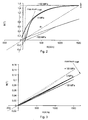
- Figure 5 shows the linearity deviation as a function of shear stresses applied to the load-carrying member for three different types of layer.
- the curve 20 is the output signal for a plated Ni-Fe layer, with 40% Fe, which is not heat-treated.
- the curve 22 is the output signal for a plated and heat-treated Ni-Fe layer, with 50% Fe
- the curve 24 is the output signal for a plated Ni layer, without Fe and not heat-treated.
- the linearity deviation is smallest for the heat-treated Ni-Fe layer.
- the measuring layer produced by the inventive method, is linear over a large load range, it is suitable for measure torques in a large load range.
- the invention makes it possible to produce a torque sensor that can measure shear stresses with high accuracy up to 300MPa.
- the present invention is not limited to the embodiments disclosed but may be varied and modified within the scope of the following claims.
- the inventive layer without undergoing a crystallization process of a nanocrystalline layer, instead the layer can be directly formed with the desired grain size and magnetic properties, for example, by means of metal spraying.
Description
- The present invention relates to a measuring device including a layer of a magnetoelastic alloy formed on a load-carrying member, which layer is intended for measuring stresses induced by a force applied to the load-carrying member, and a method for production thereof. The force applied to the load-carrying member is, for example, a tensile force, a compressive force, or a torque.
- The method according to the invention is useful for all types of measuring devices having a measuring layer on a load-carrying member. The measuring device measures stresses and/or strain in the layer, for example, induced by tensile forces, compressive forces, and torque applied to the load-carrying member. A measuring device according to the present invention may be used as a separate component in all such applications where for different reasons it is of interest to measure forces on a load-carrying member. The measuring device may, for example, be used to measure forces in, but not limited to, engines, cars, airplanes, jet engines, bicycles, gear boxes, power steering in cars, tools, propeller engines or helicopters.
- Torque sensors of the type having a stress-measuring magnetoelastic or magnetostrictive layer formed on the surface of a load-carrying member, for example a shaft, are well known in the art. The purpose of the load-carrying member is to transfer load to the stress-measuring layer. A magnetoelastic material is a material that changes its permeability when it is loaded by a force. Examples of magnetoelastic materials are iron, nickel, cobalt and rare earth metals or alloys thereof. In this application the terms magnetoelastic and magnetostrictive are used synonymously. The magnetoelastic layer is formed on the surface of the member by different methods, for example by plating, thermal spraying, metal spraying, gun coating, welding, or gluing.
-
WO0144770 -
US 5,142,227 describes a method and apparatus for measuring strain in a substrate by attaching thereto a magnetic circuit comprising a ferromagnetic element and sensing a change in the coercive field of the element caused by strain therewith. - There is a desire to be able to measure mechanical stresses in a large load range. For example, in the car industry there is a desire to measure torque-induced shear stresses of a magnitude up to 200-300MPa. Further, there is a desire to find a torque-measuring device that is long-time stable due to resistance against mechanical and thermal fatigue and is linear, i.e. the output signal from the measuring device is essentially proportional to the load on the load-carrying member. Further, there is a desire to reduce or even eliminate creeping in the output signal from the measuring device, i.e. the output signal should not change its value at a constant load. Hysteresis in the output signal should be avoided as it increases the measurement errors.
- The object of the present invention is to provide a method for producing a layer on a load-carrying member, which makes it possible to manufacture an improved device for measuring stresses induced in the layer, with respect to one or more of the above-mentioned desires and without significantly altering important properties of the load carrying member.
- This object is achieved by a method as defined in
claim 1. - Such a method comprises: forming a nanocrystalline layer of a magnetoelastic alloy having an average grain size less than 50nm on a surface of a member, and heat treating the layer until a crystallization of the alloy occurs and the average grain size becomes in the range of 100nm to 10 000nm.
- Surprisingly, it has been discovered that heating of nanocrystalline layers of magnetoelastic alloys of certain compositions, having an average grain size less than 50nm, to a certain temperature, which depends on the composition of the alloy, causes a crystallization of the alloy, which drastically improves the stress measuring properties of the layer. It is essential that the temperature to which the alloy is heated is lower than the melting temperature of the alloy. Otherwise, the desired properties will not be obtained. Advantages achieved with the method according to the invention are that the measuring layer produced by the method is essentially linear over a large load range, has a low hysteresis, and has an improved stability against ageing and fatigue.
- It has been proven by experiments that an alloy including iron, nickel and other alloying elements within certain ranges achieves the desired crystallization and obtains the desired properties, when they are heat treated to a temperature above 350°C, but less than the melting point of the layer. However, although not yet tested, it is most probable that other combinations of alloying elements in certain ratios would achieve the same result using the method according to the invention. The man skilled in the art may by due practice find out if the method works for other alloying elements as well, and within which ranges it works. For example, combinations of iron and cobalt, or nickel and cobalt would probably achieve the same result.
- In order to achieve a linear behavior over a wide range of stress amplitudes, it is important to avoid saturation of magnetic induction thus implying the need for a moderate permeability. The energy density of magnetoelastic interaction with external stress is proportional to the energy density of magnetic interaction with an external magnetic field. This proportionality depends on magnetic properties such as saturation magnetic induction, saturation magnetostriction, the magnetizing field, stress, and furthermore the size of the magnetic domains. The magnetic domain size is proportional to the permeability. To design a material with a moderate permeability, a small domain size must be achieved. One way to obtain this is to tailor a microstructure of the material with a grain size large enough to accommodate a single domain, but small enough to accommodate just one, or a few. The smallest grain size when this occurs is in the order of fractions of micrometers. A nanocrystalline layer having an average grain size less than 50nm provides favorable conditions for crystallization and tailoring the mentioned microstructure.
- According to an embodiment of the invention, the average grain size of said layer is in the range of 100 nm to 5000nm, preferably 100 nm to 1000nm, most preferably 200 nm to 500nm. Thus, more favorable conditions for the domain structure to coincide with the grain structure are created.
- As described in "Handbook of Magnetic Materials, Vol. 10, 1997, ISBN 0444825991, , there is a relation between grain size and coercive force for magnetic alloys like Ni-Fe. This would mean that the advantageous grain sizes described above would have coercive forces within certain ranges.
- According to an embodiment of the invention, the layer is heat-treated to a temperature above 300°C but less than the melting point of the layer, preferably to a temperature in the range of 350°C to 1000°C, most preferably to a temperature in the range of to 400°C to 800°C. In order to achieve the desired crystallization, the layer must be heat-treated to a temperature above the crystallization temperature of the alloy. Thus, the temperature of the heat-treatment depends on the composition of the alloy. For example, for Ni-Fe-compositions of interest the crystallization temperature is in the range of 350°C-450°C, and thus the temperature of the heat treatment must exceed this temperature. If the layer is heat-treated to a temperature in the range of 400°C to 800°C, the preferred grain structure is easier to obtain.
- According to an embodiment of the invention, the alloy includes iron in the range of 23 - 65 wt% (percent by weight), preferably 30 - 60 wt%, and most preferably 35 - 55 wt%. It has been proven that heat treatment of alloys, including iron in the range of 23 - 65 wt%, to a temperature above 350°C reduces the linearity deviation of the layer and thereby improves its measuring properties. Heat treatment of alloys, including iron in the range of 30 - 60 wt%, to a temperature above 350°C further reduces the linearity deviation and further improves the measuring properties of the alloy. Heat treatment of an alloy, including iron in the range of 35 - 55 wt%, to a temperature above 350°C significantly reduces the linearity deviation and thereby significantly improves the measuring properties of the alloy. Tests have shown that heat treatment of alloys, including less than 20 wt% iron, to a temperature above 350°C has the opposite effect, i.e. the linearity deviation increases, which results in worse measuring properties.
- The resistance against mechanical and thermal fatigue requires thermodynamic stability and stable magnetic properties. The Ni-Fe-alloy system presents these properties in the alloying range between 23% and 65%Fe. In the alloying range up to 20% the thermodynamic stability is insufficient for high service temperatures, furthermore, around 20%-23%Fe properties like the magnetostriction and crystal anisotropy change sign and display a strong dependency on chemical composition and methods of manufacturing. Above 65%Fe in Ni the Invar alloy range is approached with unsuitable magnetoelastic properties for the objective of this invention.
- According to an embodiment of the invention, the alloy further includes nickel in the range of 35 - 77 wt%, preferably 40 - 70 wt%, and most preferably 45 - 65 wt%. When an alloy, having a nickel and iron content within those ranges, is subjected to a heat treatment, according to the invention, a particularly advantageous Ni-Fe structure is formed, which has an average grain size within the desired interval and desired magnetic domains. This Ni-Fe structure has particularly advantageous magnetoelastic properties and thus improved measuring properties.
- According to an embodiment of the invention, the alloy includes less than 10 wt% of one or more other alloying elements. The other alloying elements are for example cobalt, silicon, boron, sulphur, carbon, oxygen, nitrogen, aluminum, germanium, titanium, molybdenum, niobium, silver and copper. The alloy is allowed to include less than 10 wt% of other alloying elements in order to achieve the improved measuring properties.
- According to an embodiment of the invention, the layer is heat-treated for a period of time less than 30 seconds. The heating time is not critical as long as the requirements on relative permeability and differential permeability are fulfilled. As soon as the crystallization has occurred the heating can be finished. The heat treatment should preferably be as fast as possible in order to avoid heating of the load-carrying member and thereby deteriorate its properties, such as the hardening of the member. It is advantageous to use induction heating for the heat treatment since it is fast and provides a local heating of the layer.
- According to an embodiment of the invention, said layer is formed on the member by means of electroplating. Electroplating is a suitable method in order to achieve a nanocrystalline layer of the desired grain size.
- According to an embodiment of the invention, the layer is heat-treated until a crystallization of the alloy occurs and the relative permeability becomes less than 500 and the maximum differential permeability becomes less than twice the relative permeability, both measured in a magnetizing field with an amplitude less than 1500 A/m. When those requirements on relative permeability and maximum differential permeability are fulfilled, the magnetization curve is essentially straight, which means that saturation of the magnetic induction does not occur. This is advantageous as a sensor with such a layer has an essentially linear output signal as a function of the load.
- Another object of the present invention is to provide a measuring device including a layer of a magnetoelastic alloy formed on a load-carrying member, which device is improved with respect to one or more of the above-mentioned desires.
- This object is achieved by a measuring device as defined in claim 12.
- Such a measuring device is essentially linear over a large load range, has a low hysteresis, and has an improved stability against ageing and fatigue.
- The invention is particularly useful for producing a sensor for measuring the torque of an engine or transmission, such as the engine or transmission of a car, as the torque sensor produced is linear in the desired load range for such an application.
- The invention will now be explained more closely by the description of different embodiments of the invention and with reference to the appended figures.
- Fig. 1
- shows an example of a measuring device including a load-carrying member covered with a magnetoelastic layer.
- Fig. 2
- shows an example of a magnetizing curve for a plated nanocrystalline magnetoelastic layer before heat treatment.
- Fig. 3
- shows an example of a magnetizing curve for the plated magnetoelastic layer after heat treatment to a temperature in the range of 350°C to 1000°C.
- Fig. 4
- shows an example of a magnetizing curve for the plated magnetoelastic layer after heat treatment to a temperature above 1000°C.
- Fig. 5
- is a diagram showing the linearity deviations as a function of the shear stress for different types of a magnetoelastic layer.
-
Figure 1 shows an example of a measuring device including a load-carrying member, in the form of arotary shaft 1, which is arranged to transmit a torque in any kind of mechanical transmission. The device is adapted to measure torques applied to the load-carrying member. The load-carrying member is made of a material with sufficient stiffness, for example of steel. Amagnetoelastic region 2 is provided on theshaft 1. Themagnetoelastic region 2 comprises afirst layer 3 of a magnetoelastic material, which has a substantially continuous extension and thickness in saidregion 2. In this embodiment, themagnetoelastic layer 3 is formed by plating and is mainly composed of iron and nickel. Asecond layer 4 in the form of a continuous strip is provided on thefirst layer 3. Thesecond layer 4 forms a surface pattern on thefirst layer 3. Further, the measuring device includeswindings 5a-b supplying the measuring device with an alternating magnetization field. This type of measuring device is, for example, described in more details in the international patent applicationWO01/44770 magnetoelastic layer 3 and to a method for producing such a layer. - Relative permeability:

Differential relative permeability,

Maximum µdiff is the largest differential relative permeability along the magnetization curve.
Ĥ is the maximum magnetizing field
B is the magnetic induction at H
µ 0 is the free space permeability - Hc, the coercive force, is the reverse magnetizing field needed to restore magnetic induction, B, to zero after saturation magnetization.

- According to the invention, a layer with improved measuring properties is achieved if the following conditions are fulfilled for measurements of a magnetic induction curve for the unloaded layer:

- Thus, the requirement on µr is that µr < 500 and the requirement on µdiff is that µdiff < 2µr measured for a maximum magnetizing field less than 1500A/m. When those requirements on µr and µdiff are fulfilled, the magnetization curve is essentially straight, which means that saturation of the magnetic induction does not occur. This is advantageous as it is makes it possible to produce a sensor with such a layer, which sensor has a linear output signal as a function of the load.
- In the following, a method for forming the
magnetoelastic layer 3 on themember 1 will be described. In a first step, a nanocrystalline layer of a magnetoelastic alloy having an average grain size less than 50nm is formed on the surface of the load-carryingmember 1. An average grain size less than 50nm is advantageous as it causes fast growth of the grains during the next step of the method. If the grain size is too large, the desired crystallization will not take place. Preferably, the layer should have an isotropic texture and isomorph grain structure as this represents a good starting point for the desired crystallization. - In this embodiment example, the forming is made by means of electroplating. However, it is also possible to use other methods such as PVD (Physical Vapor Deposition) methods, CVD (Chemical Vapor Deposition) methods, metal spraying, detonation gun, welding, and gluing. The thickness of the layer is typically in the range of 10-500µm. The average grain size of such a layer is less than 50nm and for example between 10nm and 15nm. The magnetoelastic layer is, for example, composed of approximately 40 wt% of iron, approximately 60 wt% of nickel and less than 1 wt% of other alloying elements.
- The layer formed by the plating is either nanocrystalline or amorphous, which is a metastable crystalline state. The layer is hard. High internal stress can occur in the layer. When the layer ages or when it is used at an increased temperature, the mechanical and magnetic properties of the layer are changing. The mechanical and magnetic properties also change when the layer is exposed to a repeated mechanical tension. This inclination to change the properties over the lifetime of the device is a bad quality for a sensor.
-
Figure 2 shows magnetization curves, i.e. the BH curve, for three different loads on the magnetoelastic layer, measured after the layer has been formed on the member and before it has been heat-treated. The curve with a thin continuous line represents -100MPa compressive stress. The dashed line represents +100MPa tensile stress. The thick continuous line represents an unloaded 0MPa layer. Magnetic induction saturation occurs when the BH curve is curved. As seen from the curves, magnetic induction saturation occurs already at zero load. For the zero load curve µr is about 800 and maximum µdiff is about 5100. Thus, maximum µdiff ≈ 6.4µr. The magnetization curves are curved and do not fulfill the requirement on µr and µdiff. A disadvantage with having such a layer in a force measuring sensor is that the output signal becomes non-linear for large loads. Another disadvantage is that a sensor with this layer is not stable over long time due to poor resistance against mechanical and thermal fatigue. - In a second step the layer is heat-treated to a temperature in the range of 350°C to 1000°C. It is enough to heat the layer until a crystallization of the alloy occurs. Typically, for an iron, nickel alloy this crystallization occurs when the layer reaches a temperature between 350 and 450°C. However, it is possible to heat the layer to a higher temperature and achieve the same type of crystallization, as long as the temperature is essentially below the melting temperature of the alloy. The desired crystallization occurs as soon as the alloy reaches the crystallization temperature. Further heating of the alloy only has a minor effect on the measuring properties. Thus, the time for the heat treatment is fast, less than 30 seconds and typically a few seconds, is enough to achieve the desired crystallization. It is important that the heat treatment is fast in order to avoid heating the load-carrying member, and thereby avoiding influencing the properties of the member. In order to avoid oxidation of the alloy, it is advantageous to use a protective gas during the heat treatment. However, it is not necessary to use a protective gas.
- The heating of the layer is for example made by means of induction heating. An advantage with induction heating is that it is fast and concentrates the heating to the magnetoelastic layer, and thus avoids heating the load-carrying member. Other possible methods for heating the layer are for example, but not limited to, laser heating, oven heating, and infrared radiation heating.
- During crystallization, a considerable growth of the grains occurs. The increase of the average grain size is about ten times the size before the crystallization. After crystallization, the average grain size becomes in the range of 100nm to 1000nm, preferably in the range of 200-500nm. The mechanical and magnetic properties after the crystallization become more stable over time and also more stable when exposed to an increased temperature.
- The structure of the electroplated material is usually nanocrystalline. Magnetic domain structure of magnetic nanocrystalline and amorphous materials are characterized by large domains, at least tenths of µm in one direction. Nanocrystalline materials are created under thermodynamically non-equilibrium conditions; hence they are in a thermodynamically metastable state. For example, nanocrystalline material having d = 10nm in grain size and D = 1nm in grain boundary is estimated to have 27.1 % of intercrystalline matter according to formula Vf ic=1-[(d-D)/d]3. In that sense nanocrystalline materials can be treated as quenched. The order of the lattice and reducing volume of the intercrystalline matter, i.e. increasing size of crystallites reduces energy and hence makes the system more stable. For example, Ni-Fe nanocrystalline material is crystallizing upon heating and forming polycrystalline material with an average grain size equal or exceeding 100nm.
- The crystallization temperature and character in Ni-Fe alloys is dependent on iron concentration, but to our knowledge the onset of crystallization does not exceed 450°C at Ni-Fe concentrations of interest. As already mentioned above the magnetic domain structure of nanocrystalline or amorphous material does not sense the crystallite structure of the material i.e. the magnetic domain wall interaction with crystallite boundary is very low. Upon crystallization, grains in the material start to become large enough and grain boundaries sharp enough for the magnetic domain to interact with them, which makes it energetically more favourable for the magnetic domain structure to break down into smaller domains. This is for example described in more detail in "Reviews on Advanced Materials Science", vol. 5, No. 2, p. 134-138, 2003 written by F.Ebrahimi and H.Q.Li and "IEEE Transactions on magnetics", vol. 27, No. 6, p. 4452 - 4457, 1991 by A.S.Kao and P.Kasiraj.
-
Figure 3 shows examples of magnetization curves for different loads on the magnetoelastic layer, measured after the layer has been heat-treated. The curve with a continuous line represents -100MPa compressive stress. The dashed line represents +100MPa tensile stress. The unloadedcurve 0 MPa is the thick continuous line. As seen from the curves, magnetic induction saturation is not present. For zero load µr is about 60 and maximum µdiff is 68. Thus, µr is about the same as the maximum µdiff. The magnetization curves are almost straight and fulfill the requirement on µr and µdiff. -
Figure 4 shows magnetization curves for different loads on the magnetoelastic layer, measured after the layer has been heat-treated to a temperature above 1000°C and below the melting temperature of the alloy. When the layer is heated to such a high temperature, the average grain size becomes larger than 1000nm. When the grain particles become too large, the properties of the layer changes and becomes less advantageous for stress measurements. The curve with a thin continuous line represents -100MPa compressive stress and the dashed line represents +100MPa tensile stress. The unloaded curve is the thick continuous line. As seen from the curves, magnetic induction saturation is beginning to appear. µr is about 375 and the maximum µdiff is about 950. Thus, µr is less than 500, but µdiff is more than twice the value of µr. The magnetization curves are beginning to curve and do not fulfill both requirement on µr and µdiff. A disadvantage with having such a layer in a force measuring sensor is that the output signal becomes non-linear due to the load. -
Figure 5 shows the linearity deviation as a function of shear stresses applied to the load-carrying member for three different types of layer. Thecurve 20 is the output signal for a plated Ni-Fe layer, with 40% Fe, which is not heat-treated. Thecurve 22 is the output signal for a plated and heat-treated Ni-Fe layer, with 50% Fe, and thecurve 24 is the output signal for a plated Ni layer, without Fe and not heat-treated. As seen from the figure, the linearity deviation is smallest for the heat-treated Ni-Fe layer. As the measuring layer, produced by the inventive method, is linear over a large load range, it is suitable for measure torques in a large load range. For example, the invention makes it possible to produce a torque sensor that can measure shear stresses with high accuracy up to 300MPa. - Through experiments it has been proven that a combination of good linearity over a wide load range, low load hysteresis, and long-term stability can be achieved for alloys of the claimed composition of and heat treatment. It has also been proved that Ni and Fe alloys with compositions outside the claimed ranges do not attain the desired properties, and that alloys heat-treated to a temperature outside the claimed temperature range do not attain the desired properties.
- The term comprises/comprising when used in this specification is taken to specify the presence of stated features, steps or components. However, the term does not preclude the presence or addition of one or more additional features, steps or components or groups thereof.
- The present invention is not limited to the embodiments disclosed but may be varied and modified within the scope of the following claims. For example it is possible to form the inventive layer without undergoing a crystallization process of a nanocrystalline layer, instead the layer can be directly formed with the desired grain size and magnetic properties, for example, by means of metal spraying.
Claims (22)
- A method for producing a layer (3) on a load-carrying member (1), which layer is intended for measuring stresses induced by a force applied to the load-carrying member, wherein the method comprises:forming a nanocrystalline layer of a magnetoelastic alloy having an average grain size less than 50nm on a surface of the member, andheat treating the layer until a crystallization of the alloy occurs and the average grain size becomes in the range of 100nm to 10 000nm.
- The method according to claim 1, wherein the average grain size of said layer is in the range of 100nm to 5000nm, preferably 100nm to 1000nm, most preferably 200nm to 500nm.
- The method according to claim 1 or 2, wherein the layer is heat-treated to a temperature above 300°C but less than the melting point of the layer, preferably to a temperature in the range of 350°C to 1000°C, most preferably to a temperature in the range of to 400°C to 800°C.
- The method according to any of the claims 1 - 3, wherein the alloy includes iron in the range of 23 - 65 wt%, preferably 30 - 60 wt%, and most preferably 35 - 55 wt%.
- The method according to claim 4, wherein the alloy includes nickel in the range of 35 - 77 wt%, preferably 40 - 70 wt%, and most preferably 45 - 65 wt%.
- The method according to claim 4 or 5, wherein the alloy includes less than 10 wt% of one or more other alloying elements.
- The method according to any of the previous claims, wherein the layer is heat-treated until a crystallization of the alloy occurs and the relative permeability (µr) becomes less than 500 and the maximum differential permeability (µdiff) becomes less than twice the relative permeability, both measured in a magnetizing field with an amplitude less than 1500 A/m.
- The method according to any of the preceding claims, wherein the heat treatment is made by means of induction heating.
- The method according to any of the preceding claims, wherein said layer is formed on the member by means of electroplating.
- The method according to any of the preceding claims, wherein the layer is heat-treated for a period of time that is less than 30 seconds.
- The method according to any of the preceding claims, wherein the layer is intended for measuring stresses induced by a torque applied on the load-carrying member.
- A measuring device including a layer (3) of a magnetoelastic alloy formed on a load-carrying member (1), which layer is intended for measuring stresses induced by a force applied to the load-carrying member, characterized in that the average grain size of said layer is in the range of 200nm to 10 000nm.
- The device according to claim 12, wherein the average grain size of said layer is in the range of 200nm to 5000nm, preferably 200nm to 1000nm, most preferably 200nm to 500nm.
- The device according to claim 12 or 13, wherein the alloy includes iron in the range of 23 - 65 wt%, preferably 30 - 60 wt%, and most preferably 35 - 55 wt%.
- The device according to claim 14, wherein the alloy includes nickel in the range of 35 - 77 wt%, preferably 40 - 70 wt%, and most preferably 45 - 65 wt%.
- The device according to claim 14 or 15, wherein the alloy includes less than 10 wt% of other alloying elements.
- The device according to any of the claims 12 -16, wherein the relative permeability (µr) is less than 500 and the maximum differential permeability (µdiff) is less than twice the relative permeability, both measured in a magnetizing field with an amplitude less than 1500 A/m.
- The device according to any of claims 12-17, wherein said stress measuring layer is obtained by forming a nanocrystalline layer of a magnetoelastic alloy having an average grain size less than 50nm on a surface of said load-carrying member, and heat treating the layer to a temperature above 300°C but less than the melting point of the layer, until a crystallization of the alloy occurs.
- The device according to any of the claim 12 - 18, wherein the measuring device is a torque sensor.
- The device according to any of the claim 12 - 18, wherein the measuring device is a force sensor.
- Use of the method according to any of the claims 1 - 11 for producing a torque sensor.
- Use of the method according to any of the claims 1 - 11 for producing a force sensor.
Applications Claiming Priority (2)
| Application Number | Priority Date | Filing Date | Title |
|---|---|---|---|
| SE0600543A SE529789C8 (en) | 2006-03-10 | 2006-03-10 | Measuring device comprising a layer of a magnetoelastic alloy and method for manufacturing the measuring device |
| PCT/SE2007/050088 WO2007106024A1 (en) | 2006-03-10 | 2007-02-14 | A measuring device including a layer of a magnetoelastic alloy and a method for production thereof |
Publications (3)
| Publication Number | Publication Date |
|---|---|
| EP2018530A1 EP2018530A1 (en) | 2009-01-28 |
| EP2018530A4 EP2018530A4 (en) | 2011-06-29 |
| EP2018530B1 true EP2018530B1 (en) | 2013-06-19 |
Family
ID=38509762
Family Applications (1)
| Application Number | Title | Priority Date | Filing Date |
|---|---|---|---|
| EP07709481.1A Active EP2018530B1 (en) | 2006-03-10 | 2007-02-14 | A measuring device including a layer of a magnetoelastic alloy and a method for production thereof |
Country Status (6)
| Country | Link |
|---|---|
| US (1) | US8316724B2 (en) |
| EP (1) | EP2018530B1 (en) |
| JP (1) | JP4931992B2 (en) |
| CN (1) | CN101416036B (en) |
| SE (1) | SE529789C8 (en) |
| WO (1) | WO2007106024A1 (en) |
Families Citing this family (9)
| Publication number | Priority date | Publication date | Assignee | Title |
|---|---|---|---|---|
| ATE533192T1 (en) * | 2008-09-25 | 2011-11-15 | Abb Ab | SENSOR FOR MEASURING MECHANICAL LOADS WITH A LAYER OF MAGNETOELASTIC MATERIAL |
| CN103439034B (en) * | 2013-09-09 | 2015-05-13 | 淮海工学院 | Multifunctional force cell sensor |
| DE102015202240B3 (en) * | 2015-02-09 | 2016-02-25 | Schaeffler Technologies AG & Co. KG | Arrangement for measuring a force or a moment with at least three magnetic field sensors |
| WO2017057750A1 (en) * | 2015-10-01 | 2017-04-06 | ヤマハ発動機株式会社 | Magnetostrictive sensor |
| CN105466998B (en) * | 2015-12-31 | 2018-11-06 | 爱德森(厦门)电子有限公司 | A method of utilizing frequency conversion varying magnetic field exciting test Testing of Ferromagnetic Material Hardness characteristic |
| CN109313006B (en) | 2016-05-17 | 2021-02-02 | 康斯博格股份有限公司 | System, method and object for high accuracy magnetic position sensing |
| WO2018109674A1 (en) | 2016-12-12 | 2018-06-21 | Kongsberg Inc. | Dual-band magnetoelastic torque sensor |
| JP2021527825A (en) * | 2018-06-21 | 2021-10-14 | トラファグ アクツィエンゲゼルシャフトTrafag Ag | Load measurement equipment, this manufacturing method, and the load measurement method that can be carried out with it. |
| DE102019005859A1 (en) * | 2019-08-20 | 2021-02-25 | Methode Electronics Malta Ltd. | Method for measuring a torque applied to a magnetoelastic body |
Family Cites Families (15)
| Publication number | Priority date | Publication date | Assignee | Title |
|---|---|---|---|---|
| US4896544A (en) * | 1986-12-05 | 1990-01-30 | Mag Dev Inc. | Magnetoelastic torque transducer |
| DE3884491T2 (en) * | 1987-07-14 | 1994-02-17 | Hitachi Metals Ltd | Magnetic core and manufacturing method. |
| DE3814348A1 (en) * | 1988-04-28 | 1989-11-09 | Philips Patentverwaltung | METHOD FOR PRODUCING A POLYCRYSTALLINE SEMICONDUCTIVE RESISTANCE LAYER FROM SILICON ON A SILICON SUPPORT |
| US5142227A (en) * | 1990-06-04 | 1992-08-25 | Allied-Signal Inc. | Method and apparatus for measuring strain within a ferromagnetic material by sensing change in coercive field |
| US5324571A (en) * | 1992-02-05 | 1994-06-28 | Konica Corporation | Magnetic recording medium comprising a support and a plurality of layers in which the magnetic layer has a specified plastic deformation |
| DE4220226A1 (en) * | 1992-06-20 | 1993-12-23 | Bosch Gmbh Robert | Magnetostrictive converter |
| US5585574A (en) * | 1993-02-02 | 1996-12-17 | Mitsubishi Materials Corporation | Shaft having a magnetostrictive torque sensor and a method for making same |
| JPH0815060A (en) * | 1994-06-28 | 1996-01-19 | Mitsubishi Materials Corp | Manufacture of magnetostrictive film for torque sensor |
| WO1999045601A2 (en) * | 1998-03-05 | 1999-09-10 | Koninklijke Philips Electronics N.V. | Magnetostrictive stress sensor |
| JPH11258077A (en) * | 1998-03-10 | 1999-09-24 | Toyota Autom Loom Works Ltd | Torque sensor |
| US6258185B1 (en) * | 1999-05-25 | 2001-07-10 | Bechtel Bwxt Idaho, Llc | Methods of forming steel |
| JP4337209B2 (en) * | 2000-02-22 | 2009-09-30 | 日立金属株式会社 | Permanent magnet thin film and manufacturing method thereof |
| JP2002107241A (en) * | 2000-09-28 | 2002-04-10 | Hitachi Metals Ltd | Torque transmission shaft and torque sensor using it |
| GB0107182D0 (en) * | 2001-03-22 | 2001-05-09 | Secr Defence | Stress sensor |
| WO2004106565A2 (en) * | 2003-05-23 | 2004-12-09 | The Nanosteel Company | Layered metallic material formed from iron based glass alloys |
-
2006
- 2006-03-10 SE SE0600543A patent/SE529789C8/en unknown
-
2007
- 2007-02-14 CN CN200780008135.0A patent/CN101416036B/en active Active
- 2007-02-14 JP JP2009500328A patent/JP4931992B2/en active Active
- 2007-02-14 EP EP07709481.1A patent/EP2018530B1/en active Active
- 2007-02-14 WO PCT/SE2007/050088 patent/WO2007106024A1/en active Application Filing
- 2007-02-14 US US12/282,352 patent/US8316724B2/en active Active
Also Published As
| Publication number | Publication date |
|---|---|
| JP2009529692A (en) | 2009-08-20 |
| US8316724B2 (en) | 2012-11-27 |
| EP2018530A4 (en) | 2011-06-29 |
| SE529789C2 (en) | 2007-11-27 |
| WO2007106024A1 (en) | 2007-09-20 |
| SE529789C8 (en) | 2007-12-27 |
| CN101416036B (en) | 2010-12-01 |
| SE0600543L (en) | 2007-09-11 |
| EP2018530A1 (en) | 2009-01-28 |
| US20090249893A1 (en) | 2009-10-08 |
| JP4931992B2 (en) | 2012-05-16 |
| CN101416036A (en) | 2009-04-22 |
Similar Documents
| Publication | Publication Date | Title |
|---|---|---|
| EP2018530B1 (en) | A measuring device including a layer of a magnetoelastic alloy and a method for production thereof | |
| JP3164590B2 (en) | Collarless circumferential magnetized torque transducer with two-phase shaft and torque measuring method using the same | |
| Li et al. | Ductility, texture and large magnetostriction of Fe–Ga-based sheets | |
| Lee et al. | High temperature microstructural evolution of 304L stainless steel as function of pre-strain and strain rate | |
| JPS63252487A (en) | Magnetoelastic torque transducer | |
| Koyama et al. | Si content dependence on shape memory and tensile properties in Fe–Mn–Si–C alloys | |
| US8272277B2 (en) | Sensor for measuring stresses including a layer of a magnetoelastic material and a method for producing the layer | |
| Baker et al. | The effect of temperature and Fe: Al ratio on the flow and fracture of FeAl | |
| JPWO2008023734A1 (en) | Fe-based alloy and manufacturing method thereof | |
| Nakajima et al. | Performance boost of co-rich fe-co based alloy magnetostrictive sensors via nitrogen treatment | |
| Alberts et al. | Magnetoelastic behaviour in dilute Cr-Co alloys | |
| Yamaura | Microstructure and magnetostriction of heavily groove-rolled Fe-Co alloy wires | |
| Li et al. | Strain rate sensitivity of Cu after severe plastic deformation by multiple compression | |
| Rho et al. | The effect of applied strain range on the fatigue cracking in Nb-A286 iron-base superalloy | |
| Huang et al. | Dynamic impact behavior and ferrite variation of special stainless steels | |
| Zhao et al. | Enhancing the formability of FeSi6. 5 steel by the anodic polarization | |
| JPH1137864A (en) | Manufacture of magnetostrictive film of magnetostrictive torque sensor | |
| JP3024817B2 (en) | Magnetostrictive detector for magnetostrictive torque sensor and method of manufacturing the same | |
| JP5648958B2 (en) | Method of manufacturing plate member for magnetostrictive force sensor, ring member for magnetostrictive force sensor, and method of manufacturing ring member for magnetostrictive force sensor | |
| DE102018009834A1 (en) | Sensor device and method for determining a torque of a torque transmission device | |
| Morrison et al. | Cyclic plasticity of polycrystalline nickel at low plastic strain amplitude: constricted hysteresis loops | |
| Saito et al. | Magnetostriction of Polycrystalline Strong-Textured Fe–17 at% Ga Laminates | |
| JP2008147244A (en) | Method for manufacturing magnetoelastic torque sensor | |
| Saito et al. | Magnetostriction of polycrystalline strong-textured Fe-17at% Ga alloy fabricated by combining rapid-solidification and sintering processes | |
| AMORPHOUS et al. | B. Hernandoa), J. Olivera, ML Sánchez, VM Prida, MJ Pérez, JD Santos and P. Gorria |
Legal Events
| Date | Code | Title | Description |
|---|---|---|---|
| PUAI | Public reference made under article 153(3) epc to a published international application that has entered the european phase |
Free format text: ORIGINAL CODE: 0009012 |
|
| 17P | Request for examination filed |
Effective date: 20080729 |
|
| AK | Designated contracting states |
Kind code of ref document: A1 Designated state(s): AT BE BG CH CY CZ DE DK EE ES FI FR GB GR HU IE IS IT LI LT LU LV MC NL PL PT RO SE SI SK TR |
|
| AX | Request for extension of the european patent |
Extension state: AL BA HR MK RS |
|
| A4 | Supplementary search report drawn up and despatched |
Effective date: 20110531 |
|
| DAX | Request for extension of the european patent (deleted) | ||
| 17Q | First examination report despatched |
Effective date: 20120913 |
|
| RIC1 | Information provided on ipc code assigned before grant |
Ipc: H01L 41/12 20060101ALI20121011BHEP Ipc: G01L 3/10 20060101AFI20121011BHEP Ipc: H01L 41/22 20060101ALI20121011BHEP |
|
| GRAP | Despatch of communication of intention to grant a patent |
Free format text: ORIGINAL CODE: EPIDOSNIGR1 |
|
| GRAS | Grant fee paid |
Free format text: ORIGINAL CODE: EPIDOSNIGR3 |
|
| GRAA | (expected) grant |
Free format text: ORIGINAL CODE: 0009210 |
|
| AK | Designated contracting states |
Kind code of ref document: B1 Designated state(s): AT BE BG CH CY CZ DE DK EE ES FI FR GB GR HU IE IS IT LI LT LU LV MC NL PL PT RO SE SI SK TR |
|
| REG | Reference to a national code |
Ref country code: GB Ref legal event code: FG4D |
|
| REG | Reference to a national code |
Ref country code: CH Ref legal event code: EP |
|
| REG | Reference to a national code |
Ref country code: AT Ref legal event code: REF Ref document number: 617906 Country of ref document: AT Kind code of ref document: T Effective date: 20130715 |
|
| REG | Reference to a national code |
Ref country code: IE Ref legal event code: FG4D |
|
| REG | Reference to a national code |
Ref country code: DE Ref legal event code: R096 Ref document number: 602007031112 Country of ref document: DE Effective date: 20130814 |
|
| PG25 | Lapsed in a contracting state [announced via postgrant information from national office to epo] |
Ref country code: SE Free format text: LAPSE BECAUSE OF FAILURE TO SUBMIT A TRANSLATION OF THE DESCRIPTION OR TO PAY THE FEE WITHIN THE PRESCRIBED TIME-LIMIT Effective date: 20130619 Ref country code: ES Free format text: LAPSE BECAUSE OF FAILURE TO SUBMIT A TRANSLATION OF THE DESCRIPTION OR TO PAY THE FEE WITHIN THE PRESCRIBED TIME-LIMIT Effective date: 20130930 Ref country code: SI Free format text: LAPSE BECAUSE OF FAILURE TO SUBMIT A TRANSLATION OF THE DESCRIPTION OR TO PAY THE FEE WITHIN THE PRESCRIBED TIME-LIMIT Effective date: 20130619 Ref country code: LT Free format text: LAPSE BECAUSE OF FAILURE TO SUBMIT A TRANSLATION OF THE DESCRIPTION OR TO PAY THE FEE WITHIN THE PRESCRIBED TIME-LIMIT Effective date: 20130619 Ref country code: GR Free format text: LAPSE BECAUSE OF FAILURE TO SUBMIT A TRANSLATION OF THE DESCRIPTION OR TO PAY THE FEE WITHIN THE PRESCRIBED TIME-LIMIT Effective date: 20130920 Ref country code: FI Free format text: LAPSE BECAUSE OF FAILURE TO SUBMIT A TRANSLATION OF THE DESCRIPTION OR TO PAY THE FEE WITHIN THE PRESCRIBED TIME-LIMIT Effective date: 20130619 |
|
| REG | Reference to a national code |
Ref country code: LT Ref legal event code: MG4D |
|
| PG25 | Lapsed in a contracting state [announced via postgrant information from national office to epo] |
Ref country code: BG Free format text: LAPSE BECAUSE OF FAILURE TO SUBMIT A TRANSLATION OF THE DESCRIPTION OR TO PAY THE FEE WITHIN THE PRESCRIBED TIME-LIMIT Effective date: 20130919 |
|
| REG | Reference to a national code |
Ref country code: NL Ref legal event code: VDEP Effective date: 20130619 |
|
| PG25 | Lapsed in a contracting state [announced via postgrant information from national office to epo] |
Ref country code: LV Free format text: LAPSE BECAUSE OF FAILURE TO SUBMIT A TRANSLATION OF THE DESCRIPTION OR TO PAY THE FEE WITHIN THE PRESCRIBED TIME-LIMIT Effective date: 20130619 |
|
| PG25 | Lapsed in a contracting state [announced via postgrant information from national office to epo] |
Ref country code: IS Free format text: LAPSE BECAUSE OF FAILURE TO SUBMIT A TRANSLATION OF THE DESCRIPTION OR TO PAY THE FEE WITHIN THE PRESCRIBED TIME-LIMIT Effective date: 20131019 Ref country code: CY Free format text: LAPSE BECAUSE OF FAILURE TO SUBMIT A TRANSLATION OF THE DESCRIPTION OR TO PAY THE FEE WITHIN THE PRESCRIBED TIME-LIMIT Effective date: 20130724 Ref country code: EE Free format text: LAPSE BECAUSE OF FAILURE TO SUBMIT A TRANSLATION OF THE DESCRIPTION OR TO PAY THE FEE WITHIN THE PRESCRIBED TIME-LIMIT Effective date: 20130619 Ref country code: BE Free format text: LAPSE BECAUSE OF FAILURE TO SUBMIT A TRANSLATION OF THE DESCRIPTION OR TO PAY THE FEE WITHIN THE PRESCRIBED TIME-LIMIT Effective date: 20130619 Ref country code: PT Free format text: LAPSE BECAUSE OF FAILURE TO SUBMIT A TRANSLATION OF THE DESCRIPTION OR TO PAY THE FEE WITHIN THE PRESCRIBED TIME-LIMIT Effective date: 20131021 Ref country code: SK Free format text: LAPSE BECAUSE OF FAILURE TO SUBMIT A TRANSLATION OF THE DESCRIPTION OR TO PAY THE FEE WITHIN THE PRESCRIBED TIME-LIMIT Effective date: 20130619 Ref country code: CZ Free format text: LAPSE BECAUSE OF FAILURE TO SUBMIT A TRANSLATION OF THE DESCRIPTION OR TO PAY THE FEE WITHIN THE PRESCRIBED TIME-LIMIT Effective date: 20130619 |
|
| PG25 | Lapsed in a contracting state [announced via postgrant information from national office to epo] |
Ref country code: NL Free format text: LAPSE BECAUSE OF FAILURE TO SUBMIT A TRANSLATION OF THE DESCRIPTION OR TO PAY THE FEE WITHIN THE PRESCRIBED TIME-LIMIT Effective date: 20130619 Ref country code: RO Free format text: LAPSE BECAUSE OF FAILURE TO SUBMIT A TRANSLATION OF THE DESCRIPTION OR TO PAY THE FEE WITHIN THE PRESCRIBED TIME-LIMIT Effective date: 20130619 Ref country code: PL Free format text: LAPSE BECAUSE OF FAILURE TO SUBMIT A TRANSLATION OF THE DESCRIPTION OR TO PAY THE FEE WITHIN THE PRESCRIBED TIME-LIMIT Effective date: 20130619 |
|
| PG25 | Lapsed in a contracting state [announced via postgrant information from national office to epo] |
Ref country code: CY Free format text: LAPSE BECAUSE OF FAILURE TO SUBMIT A TRANSLATION OF THE DESCRIPTION OR TO PAY THE FEE WITHIN THE PRESCRIBED TIME-LIMIT Effective date: 20130619 |
|
| PLBE | No opposition filed within time limit |
Free format text: ORIGINAL CODE: 0009261 |
|
| STAA | Information on the status of an ep patent application or granted ep patent |
Free format text: STATUS: NO OPPOSITION FILED WITHIN TIME LIMIT |
|
| PG25 | Lapsed in a contracting state [announced via postgrant information from national office to epo] |
Ref country code: DK Free format text: LAPSE BECAUSE OF FAILURE TO SUBMIT A TRANSLATION OF THE DESCRIPTION OR TO PAY THE FEE WITHIN THE PRESCRIBED TIME-LIMIT Effective date: 20130619 |
|
| 26N | No opposition filed |
Effective date: 20140320 |
|
| REG | Reference to a national code |
Ref country code: DE Ref legal event code: R097 Ref document number: 602007031112 Country of ref document: DE Effective date: 20140320 |
|
| PG25 | Lapsed in a contracting state [announced via postgrant information from national office to epo] |
Ref country code: LU Free format text: LAPSE BECAUSE OF FAILURE TO SUBMIT A TRANSLATION OF THE DESCRIPTION OR TO PAY THE FEE WITHIN THE PRESCRIBED TIME-LIMIT Effective date: 20140214 Ref country code: MC Free format text: LAPSE BECAUSE OF FAILURE TO SUBMIT A TRANSLATION OF THE DESCRIPTION OR TO PAY THE FEE WITHIN THE PRESCRIBED TIME-LIMIT Effective date: 20130619 |
|
| REG | Reference to a national code |
Ref country code: CH Ref legal event code: PL |
|
| GBPC | Gb: european patent ceased through non-payment of renewal fee |
Effective date: 20140214 |
|
| PG25 | Lapsed in a contracting state [announced via postgrant information from national office to epo] |
Ref country code: CH Free format text: LAPSE BECAUSE OF NON-PAYMENT OF DUE FEES Effective date: 20140228 Ref country code: LI Free format text: LAPSE BECAUSE OF NON-PAYMENT OF DUE FEES Effective date: 20140228 |
|
| REG | Reference to a national code |
Ref country code: IE Ref legal event code: MM4A |
|
| PG25 | Lapsed in a contracting state [announced via postgrant information from national office to epo] |
Ref country code: GB Free format text: LAPSE BECAUSE OF NON-PAYMENT OF DUE FEES Effective date: 20140214 Ref country code: IE Free format text: LAPSE BECAUSE OF NON-PAYMENT OF DUE FEES Effective date: 20140214 |
|
| REG | Reference to a national code |
Ref country code: FR Ref legal event code: PLFP Year of fee payment: 10 |
|
| PG25 | Lapsed in a contracting state [announced via postgrant information from national office to epo] |
Ref country code: HU Free format text: LAPSE BECAUSE OF FAILURE TO SUBMIT A TRANSLATION OF THE DESCRIPTION OR TO PAY THE FEE WITHIN THE PRESCRIBED TIME-LIMIT; INVALID AB INITIO Effective date: 20070214 |
|
| REG | Reference to a national code |
Ref country code: FR Ref legal event code: PLFP Year of fee payment: 11 |
|
| REG | Reference to a national code |
Ref country code: FR Ref legal event code: PLFP Year of fee payment: 12 |
|
| REG | Reference to a national code |
Ref country code: DE Ref legal event code: R081 Ref document number: 602007031112 Country of ref document: DE Owner name: ABB SCHWEIZ AG, CH Free format text: FORMER OWNER: ABB AB, VAESTERAS, SE |
|
| REG | Reference to a national code |
Ref country code: AT Ref legal event code: PC Ref document number: 617906 Country of ref document: AT Kind code of ref document: T Owner name: ABB SCHWEIZ AG, CH Effective date: 20180507 |
|
| REG | Reference to a national code |
Ref country code: FR Ref legal event code: TP Owner name: ABB SCHWEIZ AG, CH Effective date: 20181106 |
|
| PGFP | Annual fee paid to national office [announced via postgrant information from national office to epo] |
Ref country code: AT Payment date: 20200220 Year of fee payment: 14 |
|
| PGFP | Annual fee paid to national office [announced via postgrant information from national office to epo] |
Ref country code: TR Payment date: 20200213 Year of fee payment: 14 Ref country code: FR Payment date: 20200219 Year of fee payment: 14 |
|
| REG | Reference to a national code |
Ref country code: AT Ref legal event code: MM01 Ref document number: 617906 Country of ref document: AT Kind code of ref document: T Effective date: 20210214 |
|
| PG25 | Lapsed in a contracting state [announced via postgrant information from national office to epo] |
Ref country code: AT Free format text: LAPSE BECAUSE OF NON-PAYMENT OF DUE FEES Effective date: 20210214 |
|
| PG25 | Lapsed in a contracting state [announced via postgrant information from national office to epo] |
Ref country code: FR Free format text: LAPSE BECAUSE OF NON-PAYMENT OF DUE FEES Effective date: 20210228 |
|
| PGFP | Annual fee paid to national office [announced via postgrant information from national office to epo] |
Ref country code: IT Payment date: 20230223 Year of fee payment: 17 Ref country code: DE Payment date: 20230216 Year of fee payment: 17 |