EP2017906B1 - Verfahren zur Herstellung eines kupferkompatiblen Phasenwechselspeicherelements und entsprechendes Phasenwechselspeicherelement - Google Patents
Verfahren zur Herstellung eines kupferkompatiblen Phasenwechselspeicherelements und entsprechendes Phasenwechselspeicherelement Download PDFInfo
- Publication number
- EP2017906B1 EP2017906B1 EP07425437A EP07425437A EP2017906B1 EP 2017906 B1 EP2017906 B1 EP 2017906B1 EP 07425437 A EP07425437 A EP 07425437A EP 07425437 A EP07425437 A EP 07425437A EP 2017906 B1 EP2017906 B1 EP 2017906B1
- Authority
- EP
- European Patent Office
- Prior art keywords
- forming
- layer
- pore
- over
- tantalum
- Prior art date
- Legal status (The legal status is an assumption and is not a legal conclusion. Google has not performed a legal analysis and makes no representation as to the accuracy of the status listed.)
- Not-in-force
Links
- 230000015654 memory Effects 0.000 title claims description 78
- RYGMFSIKBFXOCR-UHFFFAOYSA-N Copper Chemical compound [Cu] RYGMFSIKBFXOCR-UHFFFAOYSA-N 0.000 title claims description 41
- 229910052802 copper Inorganic materials 0.000 title claims description 41
- 239000010949 copper Substances 0.000 title claims description 41
- 150000004770 chalcogenides Chemical class 0.000 title claims description 34
- 230000008859 change Effects 0.000 title claims description 14
- 238000000034 method Methods 0.000 title claims description 14
- 238000004519 manufacturing process Methods 0.000 title claims description 7
- 230000008569 process Effects 0.000 title description 4
- 239000011148 porous material Substances 0.000 claims description 28
- 125000006850 spacer group Chemical group 0.000 claims description 19
- 229910052715 tantalum Inorganic materials 0.000 claims description 18
- GUVRBAGPIYLISA-UHFFFAOYSA-N tantalum atom Chemical compound [Ta] GUVRBAGPIYLISA-UHFFFAOYSA-N 0.000 claims description 18
- 229910052751 metal Inorganic materials 0.000 claims description 13
- 239000002184 metal Substances 0.000 claims description 13
- 239000000758 substrate Substances 0.000 claims description 13
- 230000004888 barrier function Effects 0.000 claims description 11
- 238000009792 diffusion process Methods 0.000 claims description 9
- 229910052581 Si3N4 Inorganic materials 0.000 claims description 7
- UGACIEPFGXRWCH-UHFFFAOYSA-N [Si].[Ti] Chemical compound [Si].[Ti] UGACIEPFGXRWCH-UHFFFAOYSA-N 0.000 claims description 7
- 150000004767 nitrides Chemical class 0.000 claims description 6
- 230000005012 migration Effects 0.000 claims description 5
- 238000013508 migration Methods 0.000 claims description 5
- MZLGASXMSKOWSE-UHFFFAOYSA-N tantalum nitride Chemical compound [Ta]#N MZLGASXMSKOWSE-UHFFFAOYSA-N 0.000 claims description 5
- 238000000151 deposition Methods 0.000 claims description 4
- 238000005530 etching Methods 0.000 claims description 3
- 230000003068 static effect Effects 0.000 claims description 2
- 238000007598 dipping method Methods 0.000 claims 1
- 239000010410 layer Substances 0.000 description 42
- 239000000463 material Substances 0.000 description 28
- 238000003860 storage Methods 0.000 description 8
- 239000012782 phase change material Substances 0.000 description 5
- 238000010438 heat treatment Methods 0.000 description 3
- 229910000618 GeSbTe Inorganic materials 0.000 description 2
- 239000004020 conductor Substances 0.000 description 2
- 239000003989 dielectric material Substances 0.000 description 2
- 230000009977 dual effect Effects 0.000 description 2
- 239000004065 semiconductor Substances 0.000 description 2
- 229910008482 TiSiN Inorganic materials 0.000 description 1
- 238000003491 array Methods 0.000 description 1
- 230000006399 behavior Effects 0.000 description 1
- 230000015572 biosynthetic process Effects 0.000 description 1
- 230000001413 cellular effect Effects 0.000 description 1
- 238000004891 communication Methods 0.000 description 1
- 238000007796 conventional method Methods 0.000 description 1
- 238000002425 crystallisation Methods 0.000 description 1
- 230000008025 crystallization Effects 0.000 description 1
- 230000008021 deposition Effects 0.000 description 1
- 239000002355 dual-layer Substances 0.000 description 1
- 238000007772 electroless plating Methods 0.000 description 1
- 238000009713 electroplating Methods 0.000 description 1
- 238000005538 encapsulation Methods 0.000 description 1
- 238000005516 engineering process Methods 0.000 description 1
- -1 i.e. Substances 0.000 description 1
- QRXWMOHMRWLFEY-UHFFFAOYSA-N isoniazide Chemical compound NNC(=O)C1=CC=NC=C1 QRXWMOHMRWLFEY-UHFFFAOYSA-N 0.000 description 1
- 238000012986 modification Methods 0.000 description 1
- 230000004048 modification Effects 0.000 description 1
- 230000003287 optical effect Effects 0.000 description 1
- 238000000059 patterning Methods 0.000 description 1
- 230000000717 retained effect Effects 0.000 description 1
- 238000007493 shaping process Methods 0.000 description 1
- 238000001228 spectrum Methods 0.000 description 1
- 238000004544 sputter deposition Methods 0.000 description 1
- 239000000126 substance Substances 0.000 description 1
Images

Classifications
-
- H—ELECTRICITY
- H10—SEMICONDUCTOR DEVICES; ELECTRIC SOLID-STATE DEVICES NOT OTHERWISE PROVIDED FOR
- H10N—ELECTRIC SOLID-STATE DEVICES NOT OTHERWISE PROVIDED FOR
- H10N70/00—Solid-state devices having no potential barriers, and specially adapted for rectifying, amplifying, oscillating or switching
- H10N70/20—Multistable switching devices, e.g. memristors
- H10N70/231—Multistable switching devices, e.g. memristors based on solid-state phase change, e.g. between amorphous and crystalline phases, Ovshinsky effect
-
- H—ELECTRICITY
- H10—SEMICONDUCTOR DEVICES; ELECTRIC SOLID-STATE DEVICES NOT OTHERWISE PROVIDED FOR
- H10N—ELECTRIC SOLID-STATE DEVICES NOT OTHERWISE PROVIDED FOR
- H10N70/00—Solid-state devices having no potential barriers, and specially adapted for rectifying, amplifying, oscillating or switching
- H10N70/801—Constructional details of multistable switching devices
- H10N70/821—Device geometry
- H10N70/828—Current flow limiting means within the switching material region, e.g. constrictions
-
- H—ELECTRICITY
- H10—SEMICONDUCTOR DEVICES; ELECTRIC SOLID-STATE DEVICES NOT OTHERWISE PROVIDED FOR
- H10N—ELECTRIC SOLID-STATE DEVICES NOT OTHERWISE PROVIDED FOR
- H10N70/00—Solid-state devices having no potential barriers, and specially adapted for rectifying, amplifying, oscillating or switching
- H10N70/011—Manufacture or treatment of multistable switching devices
- H10N70/061—Shaping switching materials
- H10N70/066—Shaping switching materials by filling of openings, e.g. damascene method
-
- H—ELECTRICITY
- H10—SEMICONDUCTOR DEVICES; ELECTRIC SOLID-STATE DEVICES NOT OTHERWISE PROVIDED FOR
- H10N—ELECTRIC SOLID-STATE DEVICES NOT OTHERWISE PROVIDED FOR
- H10N70/00—Solid-state devices having no potential barriers, and specially adapted for rectifying, amplifying, oscillating or switching
- H10N70/801—Constructional details of multistable switching devices
- H10N70/821—Device geometry
- H10N70/826—Device geometry adapted for essentially vertical current flow, e.g. sandwich or pillar type devices
-
- H—ELECTRICITY
- H10—SEMICONDUCTOR DEVICES; ELECTRIC SOLID-STATE DEVICES NOT OTHERWISE PROVIDED FOR
- H10N—ELECTRIC SOLID-STATE DEVICES NOT OTHERWISE PROVIDED FOR
- H10N70/00—Solid-state devices having no potential barriers, and specially adapted for rectifying, amplifying, oscillating or switching
- H10N70/801—Constructional details of multistable switching devices
- H10N70/841—Electrodes
- H10N70/8413—Electrodes adapted for resistive heating
-
- H—ELECTRICITY
- H10—SEMICONDUCTOR DEVICES; ELECTRIC SOLID-STATE DEVICES NOT OTHERWISE PROVIDED FOR
- H10N—ELECTRIC SOLID-STATE DEVICES NOT OTHERWISE PROVIDED FOR
- H10N70/00—Solid-state devices having no potential barriers, and specially adapted for rectifying, amplifying, oscillating or switching
- H10N70/801—Constructional details of multistable switching devices
- H10N70/841—Electrodes
- H10N70/8416—Electrodes adapted for supplying ionic species
-
- H—ELECTRICITY
- H10—SEMICONDUCTOR DEVICES; ELECTRIC SOLID-STATE DEVICES NOT OTHERWISE PROVIDED FOR
- H10N—ELECTRIC SOLID-STATE DEVICES NOT OTHERWISE PROVIDED FOR
- H10N70/00—Solid-state devices having no potential barriers, and specially adapted for rectifying, amplifying, oscillating or switching
- H10N70/801—Constructional details of multistable switching devices
- H10N70/881—Switching materials
- H10N70/882—Compounds of sulfur, selenium or tellurium, e.g. chalcogenides
- H10N70/8828—Tellurides, e.g. GeSbTe
Definitions
- the present invention relates generally to phase change memories that use chalcogenide materials.
- Phase change memory devices use phase change materials, i.e., materials that may be electrically switched between a generally amorphous and a generally crystalline state, for electronic memory application.
- phase change materials i.e., materials that may be electrically switched between a generally amorphous and a generally crystalline state, for electronic memory application.
- One type of memory element utilizes a phase change material that is electrically switched between a structural state of generally amorphous and generally crystalline local order or between different detectable states of local order across the entire spectrum between completely amorphous and completely crystalline states.
- the state of the phase change materials is also non-volatile in that, when set in either a crystalline, semi-crystalline, amorphous, or semi-amorphous state representing a resistance value, that value is retained until changed by another programming event, as that value represents a phase or physical state of the material (e.g., crystalline or amorphous). The state is unaffected by removing electrical power.
- each memory cell comprises a phase-change storage element and a selection element (such as an MOS transistor or a diode), coupled to the phase-change storage element.
- a selection element such as an MOS transistor or a diode
- a phase-change storage element comprises a resistive element (also called a heater) and a programmable element made of a chalcogenide, also called memory element.
- the resistive element and the programmable element are formed by physical stacking of layers including an ovonic unified memory (OUM).
- OUM ovonic unified memory
- the memory cells are addressed through metal lines or connections of copper, forming row and column lines. Therefore, when the cells are made using the OUM technology, their manufacturing should be compatible with copper backend step. That is, migration of copper into the chalcogenide layers forming the programmable elements should be prevented in order not to compromise the electrical characteristics of the memory cell.
- a heater is formed in pore on a copper row line and a chalcogenide region, in the form of islands or strips arranged over the pore, is obtained by shaping a chalcogenide layer.
- the heater is made of titanium silicon nitride and extends from the row line to the chalcogenide region.
- US 2004/0113136 A discloses a phase change memory comprising a semiconductor word line in substrate and a plug formed on the word line.
- the plug comprises An inner conductor region, of copper, separated from the word line by a barrier material.
- An electrode couples the inner conductor region of the plug to a line of phase change material, whereby a memory element is formed at the interface of the electrode and the line of phase change material.
- phase change memories are described in US 2003/0108674 A , in US 2002/0080647 A and in EP-A-1 677 372 , while PETERS L: "Making a better copper barrier” SEMICONDUCTOR INTERNATIONAL CAHNERS PUBLISHING USA, vol. 26, no. 3, March 2003 (2003-03), pages 50-54 , deals with barrier materials.
- the object of the invention is thus to provide a phase change memory device and the manufacturing process thereof that are compatible with copper.
- the chalcogenide that forms the memory element is isolated from the copper used for interconnects.
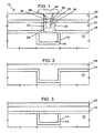
- FIG. 1 shows a phase-change storage element 10 including a memory element of a chalcogenide material.
- the phase-change storage element 10 is connected to a selection device such as an ovonic threshold switch, in a per se known manner, not shown in the drawings, to form a memory cell.
- the memory cells are arranged in row and column, to form a memory array of a memory device.
- a substrate 12 of a dielectric material, such as oxide, has a copper line 16 formed therein in a damascene process.
- the copper line 16 forms a row line and is separated from the substrate 12 by a seed layer 14, which may be any conventional copper seed layer made up of one or more elements.
- a first dielectric level 18, 20 extends over the substrate 12.
- the dielectric level 18, 20 may comprise a nitride layer 18 covered by an oxide layer 20. However, other dielectric materials may be utilized.
- the dielectric layer 18, 20 has a pore extending through it, aligned with the copper line 16.
- a plug 21 made up of multiple layers of metal is formed in the pore.
- the plug 21 comprises a first metal layer 22 which is U-shaped and may be formed of tantalum.
- a second metal layer 24 extends on top of the first metal layer 22, is also U-shaped and may be formed of tantalum nitride.
- a center region 26 of the plug 21 may be formed of titanium silicon nitride. The plug 21 reduces copper migration from the copper line 16 into the overlying chalcogenide.
- a second dielectric level 28, 30 extends on top of the first dielectric level 18, 20.
- the second dielectric level 28, 30 may include one or more layers.
- a nitride layer 28 is covered by an oxide layer 30.
- the second dielectric level 28, 30 has an opening extending through it and aligned with the pore. The opening accommodates a pair of spacers 32 and 34. However, more or less spacers may be used.
- a heater 38 e.g. of titanium silicon nitride, and a memory element 36 of chalcogenide material, e.g. of GeSbTe (GST), extend inside the spacers 32, 34, within the opening defined by the second dielectric level.
- the memory element 36 extends over the heater 38, here having a lance shape.
- a top electrode 40 extends over the opening, is aligned and in contact with the memory element 36.
- the top electrode 40 is patterned with a lithographic etch step and covered with a nitride encapsulation layer, not shown. Subsequently, an oxide layer may be deposited and polished. Then trenches are patterned; subsequently a seed layer and copper are deposited in the trenches to form column lines (not shown).
- the plug 21 is effective to reduce migration of copper from the copper line 16 upwardly to the overlying memory element 26 of chalcogenide material.
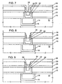
- the memory cell 10 of Figure 1 may be manufactured as shown in Figures 2-10 .
- the fabrication sequence begins, as shown in Figure 2 , by forming a damascene structure in the first dielectric level 12.
- the first dielectric level 12 is etched to form the first pore, then the seed layer 14 is deposited.
- a copper layer 16 is then blanket deposited over the seed layer 14. Any conventional technique for the deposition or formation of the copper layer 16 may be utilized, including electroplating, electroless plating, or sputtering. Thereafter, the copper layer 16 and the seed layer 14 are planarized, Figure 3 .
- the first dielectric level 18, 20 is formed over the substrate 12.
- the first dielectric level 18, 20 includes the nitride layer 18, covered by the oxide layer 20 of greater thickness, as shown in Figure 3 .
- a pore is formed through the first dielectric level 18, 20 and the pore is filled with the plug 21.
- the plug is made up of three different materials, including a first metal layer 22 of tantalum, a second metal layer 24 of tantalum nitride, and a third metal layer 26 of titanium silicon nitride.
- the tantalum nitride and tantalum are preferably not included within the upper portion that contacts the subsequently deposited chalcogenide because tantalum diffusion into the chalcogenide may reduce the heater resistance, which could compromise the cell electrical behavior.
- Extensive oxide over polish may be used to reduce underlying copper row topology. This may be done to avoid dished areas which can trap chalcogenide material in the subsequent chalcogenide chemical mechanical planarization step.
- the nitride layer 28 and the oxide layer 30 are deposited and patterned.
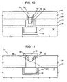
- the opening is formed through the second dielectric level 28, 30 and a dual layer spacer 32, 34 is formed.
- the use of a dual spacer layer 32, 34 reduces the diameter of the heater 38 and minimizes the heater seam.
- a first spacer layer 32 is deposited to cover the walls of the opening and is anisotropically etched to remove it from the bottom of the opening and over the second dielectric layer 30, 32.
- the spacer 32 shown in Figure 7 is formed.
- the second spacer layer 34 is deposited and, likewise, anisotropically etched to remove it from the bottom of the opening and over the second dielectric layer 30, 32.
- the dual spacers structure 32, 34 shown in Figure 8 is obtained.
- a heater layer 38 e.g. of titanium silicon nitride, is subsequently deposited into the resulting pore, as shown in Figure 9 . Then, the heater layer 38 is etched back to reduce its vertical height. The heater layer 38 may be removed using a dip back or wet or dry etch back. This etching back of the heater 38 leaves a recess wherein a chalcogenide layer 36 is deposited, as shown in Figure 9 .
- the chalcogenide layer 36 is polished back in a chemical-mechanical planarization step, thus forming the memory element 36 of Figure 10 .
- the top electrode 40 is deposited, patterned, and etched to create the structure shown in Figure 1 .
- the plug 21 is only formed by a metal region 26, e.g. of TiSiN.
- a metal region 26 e.g. of TiSiN.
- the spacers 32 and 34 are formed, as described above, and the heater 38 and the memory element 36 are formed thereover, still within the same pore as the plug 21.
- a lance structure that includes the heater 38 and the memory element 36 is self-aligned to the plug 21.
- the plug 21 may be formed by a multilayer of different metal layers, analogously to Figure 1 .
- Programming of the memory element 36 to alter the state or phase of the material may be accomplished by applying voltage potentials to the copper line 16, formed on substrate 12, and top electrode 40, thereby generating a voltage potential across the phase-change storage element 10.
- the voltage potential is greater than the threshold voltage of the memory element 36, then an electrical current may flow through the memory element 36, and results in heating of the memory element 36 by the heater 38.
- This heating may alter the memory state or phase of the memory element 36. Altering the phase or state of the memory element 36 alters the electrical characteristic of the chalcogenide material, e.g., the resistance of the material.
- memory material In the "reset” state, memory material is in an amorphous or semi-amorphous state and in the “set” state, memory material is in a crystalline or semi-crystalline state. Both “reset” and “set” states can exist without any energy (electrical, optical, mechanical) applied to bistable chalcogenide.
- the resistance of memory material in the amorphous or semi-amorphous state is greater than the resistance of memory material in the crystalline or semi-crystalline state. It is to be appreciated that the association of reset and set with amorphous and crystalline states, respectively, is a convention and that at least an opposite convention may be adopted.
- memory material may be heated to a relatively higher temperature to amorphosize memory material and "reset” memory material (e.g., program memory material to a logic "0" value). Heating the volume of memory material to a relatively lower crystallization temperature crystallizes memory material and "set” memory material (e.g., program memory material to a logic "1” value).
- Various resistances of memory material may be achieved to store information by varying the amount of current flow and duration through the volume of memory material.
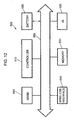
- System 500 may be used in wireless or mobile devices such as, for example, a personal digital assistant (PDA), a laptop or portable computer with wireless capability, a web tablet, a wireless telephone, a pager, an instant messaging device, a digital music player, a digital camera, or other devices that may be adapted to transmit and/or receive information wirelessly.
- PDA personal digital assistant
- System 500 may be used in any of the following systems: a wireless local area network (WLAN) system, a wireless personal area network (WPAN) system, a cellular network, although the scope of the present invention is not limited in this respect.
- WLAN wireless local area network
- WPAN wireless personal area network
- cellular network although the scope of the present invention is not limited in this respect.
- System 500 includes a controller 510, an input/output (I/O) device 520 (e.g. a keypad, display), static random access memory (SRAM) 560, a memory 530, and a wireless interface 540 coupled to each other via a bus 550.
- I/O input/output
- SRAM static random access memory
- a battery 580 is used in some embodiments.
- Controller 510 may comprise, for example, one or more microprocessors, digital signal processors, microcontrollers, or the like.
- Memory 530 may be used to store messages transmitted to or by system 500. Memory 530 may also optionally be used to store instructions that are executed by controller 510 during the operation of system 500, and may be used to store user data.
- Memory 530 may be provided by one or more different types of memory. For example, memory 530 may comprise any type of random access memory, a volatile memory, a non-volatile memory such as a flash memory, besides of memory device having the phase change storage element 10 discussed herein.
- I/O device 520 may be used by a user to generate a message.
- System 500 may use wireless interface 540 to transmit and receive messages to and from a wireless communication network with a radio frequency (RF) signal.
- RF radio frequency
- Examples of wireless interface 540 include an antenna or a wireless transceiver, although the scope of the present invention is not limited in this respect.
- the process as described herein is completely compatible with conventional copper interconnect lines, thereby allowing stackable phase change memory array layers. Also, the problems associated with dot patterning of the chalcogenide material may be reduced.
Landscapes
- Engineering & Computer Science (AREA)
- Manufacturing & Machinery (AREA)
- Semiconductor Memories (AREA)
Claims (20)
- Verfahren zur Herstellung eines kupferkompatiblen Chalcogenid-Phasenwechselspeichers, aufweisend:Ausbilden eines Substrats (12);Ausbilden einer Kuper-Zeilenleitung (16) in dem Substrat;Ausbilden einer Pore über der Kupfer-Zeilenleitung;Ausbilden eines Pfropfens (21) in der Pore, um die Wanderung von Kupfer von der Kupfer-Zeilenleitung nach oben in die Pore zu blockieren;Ausbilden eines Chalcogenidbereichs (36) in der Pore über dem Pfropfen; undAusbilden eines Erhitzers (38) in der Pore unter dem Chalcogenidbereich (36) und über dem Pfropfen (21).
- Verfahren nach Anspruch 1, bei dem das Ausbilden eines Propfens (21) ein Ausbilden von mehreren Schichten (22, 24, 26) aufweist.
- Verfahren nach Anspruch 2, bei dem das Ausbilden von mehreren Schichten ein Ausbilden einer Schicht (22, 24) auf Tantalbasis und das Ausbilden einer Metallschicht (26), die kein Tantal enthält, welche die Schicht auf Tantalbasis von dem Chalcogenidbereich (36) trennt, umfasst.
- Verfahren nach Anspruch 3, bei dem das Ausbilden einer Schicht (22, 24) auf Tantalbasis ein Ausbilden einer Tantalschicht (22) und einer Tantalnitrid-Schicht (24), wobei die Tantalnitrid-Schicht über der Tantalschicht ausgebildet wird, umfasst.
- Verfahren nach Anspruch 3, bei dem das Ausbilden einer Metallschicht (26) ein Ausbilden einer Titansiliciumnitrid-Schicht über der Schicht (22, 24) auf Tantalbasis umfasst.
- Verfahren nach einem der Ansprüche 1 bis 5, bei dem das Ausbilden einer Pore und das Ausbilden eines Pfropfens (21) ein Ausbilden einer ersten dielektrischen Ebene (18, 20) über dem Substrat (12), ein Ätzen der ersten dielektrischen Ebene, ein Abscheiden einer Pfropfenschicht (22, 24, 26) und dann ein Planarisieren der Pfropfenschicht aufweist.
- Verfahren nach Anspruch 6, bei dem das Ausbilden eines Chalcogenidbereichs (36) ein Abscheiden einer zweiten dielektrischen Ebene (28, 30) über der ersten dielektrischen Schicht (18, 20), ein Ausbilden einer Öffnung in der zweiten dielektrischen Ebene, wobei die Öffnung ein Teil der Pore ist, und ein Ausbilden des Chalcogenidbereichs (36) in der Öffnung umfasst.
- Verfahren nach einem der Ansprüche 1 bis 5, bei dem das Ausbilden einer Pore und das Ausbilden eines Pfropfens (21) ein Ausbilden einer ersten dielektrischen Ebene (18, 20) über dem Substrat (12), ein Ätzen der ersten dielektrischen Ebene, um die Pore zu bilden, ein Abscheiden einer Pfropfenschicht (22, 24, 26) und dann ein teilweises Zurückätzen der Pfropfenschicht aufweist.
- Verfahren nach einem der Ansprüche 1 bis 8, umfassend ein Ausbilden einer Trennelementstruktur (32, 24) über dem Pfropfen (21) in der Pore.
- Verfahren nach Anspruch 7, umfassend ein Ausbilden einer Trennelementstruktur (32, 24) über dem Pfropfen (21) in der Öffnung vor dem Ausbilden des Chalcogenidbereichs (36).
- Verfahren nach Anspruch 9 oder 10, bei dem das Ausbilden einer Trennelementstruktur (32, 24) ein Ausbilden eines Paares von überlappenden Seitenwand-Trennelementen aufweist.
- Phasenwechsel-Speicherelement (10) aufweisend:ein Substrat (12);eine Kupfer-Zeilenleitung (16) in dem Substrat;eine Pore über der Kupfer-Zeilenleitung (16);eine Kupfer-Diffusionssperre (21) über der Kupfer-Zellenauswahlleitung, wobei die Kupfer-Diffusionssperre einen Pfropfen in der Pore umfasst, um die Wanderung von Kupfer von der Kupfer-Zeilenleitung nach oben in die Pore zu blockieren; undeinen Chalcogenidbereich (36) über der Kupfer-Diffusionssperre; undeinen Erhitzer (38) in der Pore unter dem Chalcogenidbereich (36) und über dem Pfropfen.
- Speicherelement nach Anspruch 12, bei dem die Kupfer-Diffusionssperre (21) einen Bereich (22, 24) auf Tantalbasis umfasst.
- Speicherelement nach Anspruch 13, bei dem der Bereich (22, 24) auf Tantalbasis eine Tantalschicht (22) und eine Nitridschicht (24), die die Tantalschicht (22) bedeckt, umfasst.
- Speicherelement nach Anspruch 13 oder 14, wobei die Kupfer-Diffusionssperre außerdem eine Tantal-Diffusionssperre (26), die die Schicht auf Tantalbasis von dem Chalcogenidbereich (36) trennt, aufweist.
- Speicherelement nach Anspruch 15, bei dem die Tantal-Diffusionssperre (26) Titansiliciumnitrid umfasst.
- Speicherelement nach einem der Ansprüche 12 bis 16, aufweisend eine erste dielektrische Ebene (18, 20) über dem Substrat (12), eine Pore in der ersten dielektrischen Ebene über der Kupfer-Diffusionssperre (26), wobei die Pore eine Seitenwand-Trennelementstruktur (32, 34) und den Chalcogenidbereich (36) im inneren der Seitenwand-Trennelementstruktur aufnimmt.
- Speicherelement nach Anspruch 17, bei dem die Seitenwand-Trennelementstruktur (32, 34) ein Paar von überlappenden Seitenwand-Trennelementen umfasst.
- Speicherelement nach Anspruch 17 oder 18, außerdem aufweisend eine zweite dielektrische Ebene (28, 30) über der ersten dielektrischen Schicht (18, 20), wobei die zweite dielektrische Ebene eine Öffnung, die Teil der Pore ist, hat, wobei sich die Seitenwand-Trennelementstruktur (32, 34) und der Chaicogenidbereich (36) in der Öffnung in der zweiten dielektrischen Ebene erstrecken.
- System aufweisend:einen Prozessor (510);einen statischen Speicher mit wahlfreiem Zugriff (560), der an den Prozessor gekoppelt ist; undeinen Speicher (530), der an den Prozessor gekoppelt ist, wobei der Speicher das Speicherelement (10) nach einem der Ansprüche 12 bis 19 aufweist.
Priority Applications (3)
| Application Number | Priority Date | Filing Date | Title |
|---|---|---|---|
| EP07425437A EP2017906B1 (de) | 2007-07-17 | 2007-07-17 | Verfahren zur Herstellung eines kupferkompatiblen Phasenwechselspeicherelements und entsprechendes Phasenwechselspeicherelement |
| DE602007013386T DE602007013386D1 (de) | 2007-07-17 | 2007-07-17 | Verfahren zur Herstellung eines kupferkompatiblen Phasenwechselspeicherelements und entsprechendes Phasenwechselspeicherelement |
| US12/174,462 US8222627B2 (en) | 2007-07-17 | 2008-07-16 | Process for manufacturing a copper compatible chalcogenide phase change memory element and corresponding phase change memory element |
Applications Claiming Priority (1)
| Application Number | Priority Date | Filing Date | Title |
|---|---|---|---|
| EP07425437A EP2017906B1 (de) | 2007-07-17 | 2007-07-17 | Verfahren zur Herstellung eines kupferkompatiblen Phasenwechselspeicherelements und entsprechendes Phasenwechselspeicherelement |
Publications (2)
| Publication Number | Publication Date |
|---|---|
| EP2017906A1 EP2017906A1 (de) | 2009-01-21 |
| EP2017906B1 true EP2017906B1 (de) | 2011-03-23 |
Family
ID=38828493
Family Applications (1)
| Application Number | Title | Priority Date | Filing Date |
|---|---|---|---|
| EP07425437A Not-in-force EP2017906B1 (de) | 2007-07-17 | 2007-07-17 | Verfahren zur Herstellung eines kupferkompatiblen Phasenwechselspeicherelements und entsprechendes Phasenwechselspeicherelement |
Country Status (3)
| Country | Link |
|---|---|
| US (1) | US8222627B2 (de) |
| EP (1) | EP2017906B1 (de) |
| DE (1) | DE602007013386D1 (de) |
Families Citing this family (11)
| Publication number | Priority date | Publication date | Assignee | Title |
|---|---|---|---|---|
| US9203024B2 (en) * | 2007-07-25 | 2015-12-01 | Intel Corporation | Copper compatible chalcogenide phase change memory with adjustable threshold voltage |
| US8298937B2 (en) * | 2009-06-12 | 2012-10-30 | International Business Machines Corporation | Interconnect structure fabricated without dry plasma etch processing |
| US8907321B2 (en) * | 2009-12-16 | 2014-12-09 | Lehigh Univeristy | Nitride based quantum well light-emitting devices having improved current injection efficiency |
| US8530875B1 (en) * | 2010-05-06 | 2013-09-10 | Micron Technology, Inc. | Phase change memory including ovonic threshold switch with layered electrode and methods for forming same |
| US8409915B2 (en) * | 2010-09-20 | 2013-04-02 | Micron Technology, Inc. | Methods of forming memory cells |
| US8803122B2 (en) * | 2012-07-31 | 2014-08-12 | Globalfoundries Singapore Pte. Ltd. | Method for forming a PCRAM with low reset current |
| US9166158B2 (en) | 2013-02-25 | 2015-10-20 | Micron Technology, Inc. | Apparatuses including electrodes having a conductive barrier material and methods of forming same |
| US9172036B2 (en) | 2013-11-22 | 2015-10-27 | Taiwan Semiconductor Manufacturing Co., Ltd. | Top electrode blocking layer for RRAM device |
| US9627612B2 (en) | 2014-02-27 | 2017-04-18 | International Business Machines Corporation | Metal nitride keyhole or spacer phase change memory cell structures |
| US9281473B1 (en) * | 2015-03-13 | 2016-03-08 | Kabushiki Kaisha Toshiba | Memory device |
| US12219784B2 (en) | 2020-07-22 | 2025-02-04 | Micron Technology, Inc. | Memory device and method for manufacturing the same |
Citations (1)
| Publication number | Priority date | Publication date | Assignee | Title |
|---|---|---|---|---|
| EP1764837A1 (de) * | 2005-09-14 | 2007-03-21 | STMicroelectronics S.r.l. | Halbleiteranordnung, insbesondere Phasenwechselspeicher-Anordnung mit einheitlicher Heizelementhöhe |
Family Cites Families (10)
| Publication number | Priority date | Publication date | Assignee | Title |
|---|---|---|---|---|
| US6569705B2 (en) * | 2000-12-21 | 2003-05-27 | Intel Corporation | Metal structure for a phase-change memory device |
| US7081271B2 (en) * | 2001-12-07 | 2006-07-25 | Applied Materials, Inc. | Cyclical deposition of refractory metal silicon nitride |
| US6744088B1 (en) * | 2002-12-13 | 2004-06-01 | Intel Corporation | Phase change memory device on a planar composite layer |
| US6946397B2 (en) * | 2003-11-17 | 2005-09-20 | Taiwan Semiconductor Manufacturing Company, Ltd. | Chemical mechanical polishing process with reduced defects in a copper process |
| US7211507B2 (en) * | 2004-06-02 | 2007-05-01 | International Business Machines Corporation | PE-ALD of TaN diffusion barrier region on low-k materials |
| US7135696B2 (en) * | 2004-09-24 | 2006-11-14 | Intel Corporation | Phase change memory with damascene memory element |
| DE602004013816D1 (de) * | 2004-12-30 | 2008-06-26 | St Microelectronics Srl | Phasenwechselspeicher und Herstellungsmethode dafür |
| US7494849B2 (en) * | 2005-11-03 | 2009-02-24 | Cswitch Inc. | Methods for fabricating multi-terminal phase change devices |
| US20080157268A1 (en) * | 2006-12-30 | 2008-07-03 | Kim Deok-Kee | Fuse Element Using Low-K Dielectric |
| US20090039331A1 (en) * | 2007-08-07 | 2009-02-12 | International Business Machines Corporation | Phase change material structures |
-
2007
- 2007-07-17 EP EP07425437A patent/EP2017906B1/de not_active Not-in-force
- 2007-07-17 DE DE602007013386T patent/DE602007013386D1/de active Active
-
2008
- 2008-07-16 US US12/174,462 patent/US8222627B2/en active Active
Patent Citations (1)
| Publication number | Priority date | Publication date | Assignee | Title |
|---|---|---|---|---|
| EP1764837A1 (de) * | 2005-09-14 | 2007-03-21 | STMicroelectronics S.r.l. | Halbleiteranordnung, insbesondere Phasenwechselspeicher-Anordnung mit einheitlicher Heizelementhöhe |
Also Published As
| Publication number | Publication date |
|---|---|
| US20090050872A1 (en) | 2009-02-26 |
| US8222627B2 (en) | 2012-07-17 |
| EP2017906A1 (de) | 2009-01-21 |
| DE602007013386D1 (de) | 2011-05-05 |
Similar Documents
| Publication | Publication Date | Title |
|---|---|---|
| EP2017906B1 (de) | Verfahren zur Herstellung eines kupferkompatiblen Phasenwechselspeicherelements und entsprechendes Phasenwechselspeicherelement | |
| US8614135B2 (en) | Methods of manufacturing phase change memory devices | |
| US8377741B2 (en) | Self-heating phase change memory cell architecture | |
| EP1729355B1 (de) | Selbstjustiertes Verfahren zur Herstellung von Phasenwechselspeicherzellen | |
| US9159915B2 (en) | Phase change memory with threshold switch select device | |
| US8513576B2 (en) | Dual resistance heater for phase change devices and manufacturing method thereof | |
| US8067761B2 (en) | Self-aligned memory cells and method for forming | |
| US7838860B2 (en) | Integrated circuit including vertical diode | |
| US8404514B2 (en) | Fabricating current-confining structures in phase change memory switch cells | |
| US7709822B2 (en) | Phase change memory and manufacturing method thereof | |
| CN101552282B (zh) | 相变存储器件及其制造方法 | |
| JP2011014909A (ja) | 自己整列式縦ヒータと低抵抗率界面を備えた相変化メモリセル | |
| US20100163826A1 (en) | Method for active pinch off of an ovonic unified memory element | |
| US8026173B2 (en) | Semiconductor structure, in particular phase change memory device having a uniform height heater | |
| KR101511421B1 (ko) | 다층 상변화 물질을 이용하는 3차원 메모리 | |
| US9203024B2 (en) | Copper compatible chalcogenide phase change memory with adjustable threshold voltage | |
| US7973302B2 (en) | Forming phase change memory cells | |
| KR102357987B1 (ko) | 가변 저항 메모리 소자 및 이의 제조 방법 | |
| US7579210B1 (en) | Planar segmented contact | |
| KR20070069767A (ko) | 상변환 기억 소자 및 그의 제조방법 |
Legal Events
| Date | Code | Title | Description |
|---|---|---|---|
| PUAI | Public reference made under article 153(3) epc to a published international application that has entered the european phase |
Free format text: ORIGINAL CODE: 0009012 |
|
| AK | Designated contracting states |
Kind code of ref document: A1 Designated state(s): AT BE BG CH CY CZ DE DK EE ES FI FR GB GR HU IE IS IT LI LT LU LV MC MT NL PL PT RO SE SI SK TR |
|
| AX | Request for extension of the european patent |
Extension state: AL BA HR MK RS |
|
| 17P | Request for examination filed |
Effective date: 20090318 |
|
| 17Q | First examination report despatched |
Effective date: 20090417 |
|
| AKX | Designation fees paid |
Designated state(s): DE FR GB IT |
|
| RAP1 | Party data changed (applicant data changed or rights of an application transferred) |
Owner name: STMICROELECTRONICS SRL |
|
| GRAP | Despatch of communication of intention to grant a patent |
Free format text: ORIGINAL CODE: EPIDOSNIGR1 |
|
| GRAS | Grant fee paid |
Free format text: ORIGINAL CODE: EPIDOSNIGR3 |
|
| GRAA | (expected) grant |
Free format text: ORIGINAL CODE: 0009210 |
|
| AK | Designated contracting states |
Kind code of ref document: B1 Designated state(s): DE FR GB IT |
|
| REG | Reference to a national code |
Ref country code: GB Ref legal event code: FG4D |
|
| REF | Corresponds to: |
Ref document number: 602007013386 Country of ref document: DE Date of ref document: 20110505 Kind code of ref document: P |
|
| REG | Reference to a national code |
Ref country code: DE Ref legal event code: R096 Ref document number: 602007013386 Country of ref document: DE Effective date: 20110505 |
|
| PLBE | No opposition filed within time limit |
Free format text: ORIGINAL CODE: 0009261 |
|
| STAA | Information on the status of an ep patent application or granted ep patent |
Free format text: STATUS: NO OPPOSITION FILED WITHIN TIME LIMIT |
|
| 26N | No opposition filed |
Effective date: 20111227 |
|
| REG | Reference to a national code |
Ref country code: DE Ref legal event code: R097 Ref document number: 602007013386 Country of ref document: DE Effective date: 20111227 |
|
| PG25 | Lapsed in a contracting state [announced via postgrant information from national office to epo] |
Ref country code: IT Free format text: LAPSE BECAUSE OF FAILURE TO SUBMIT A TRANSLATION OF THE DESCRIPTION OR TO PAY THE FEE WITHIN THE PRESCRIBED TIME-LIMIT Effective date: 20110323 |
|
| PGFP | Annual fee paid to national office [announced via postgrant information from national office to epo] |
Ref country code: GB Payment date: 20130626 Year of fee payment: 7 |
|
| PGFP | Annual fee paid to national office [announced via postgrant information from national office to epo] |
Ref country code: DE Payment date: 20130621 Year of fee payment: 7 |
|
| PGFP | Annual fee paid to national office [announced via postgrant information from national office to epo] |
Ref country code: FR Payment date: 20130722 Year of fee payment: 7 |
|
| REG | Reference to a national code |
Ref country code: DE Ref legal event code: R119 Ref document number: 602007013386 Country of ref document: DE |
|
| GBPC | Gb: european patent ceased through non-payment of renewal fee |
Effective date: 20140717 |
|
| REG | Reference to a national code |
Ref country code: FR Ref legal event code: ST Effective date: 20150331 |
|
| PG25 | Lapsed in a contracting state [announced via postgrant information from national office to epo] |
Ref country code: DE Free format text: LAPSE BECAUSE OF NON-PAYMENT OF DUE FEES Effective date: 20150203 |
|
| REG | Reference to a national code |
Ref country code: DE Ref legal event code: R119 Ref document number: 602007013386 Country of ref document: DE Effective date: 20150203 |
|
| PG25 | Lapsed in a contracting state [announced via postgrant information from national office to epo] |
Ref country code: FR Free format text: LAPSE BECAUSE OF NON-PAYMENT OF DUE FEES Effective date: 20140731 Ref country code: GB Free format text: LAPSE BECAUSE OF NON-PAYMENT OF DUE FEES Effective date: 20140717 |