EP2016431B1 - Input by-pass circuit for a current probe - Google Patents
Input by-pass circuit for a current probe Download PDFInfo
- Publication number
- EP2016431B1 EP2016431B1 EP07761915.3A EP07761915A EP2016431B1 EP 2016431 B1 EP2016431 B1 EP 2016431B1 EP 07761915 A EP07761915 A EP 07761915A EP 2016431 B1 EP2016431 B1 EP 2016431B1
- Authority
- EP
- European Patent Office
- Prior art keywords
- current
- coupled
- switches
- current probe
- signal
- Prior art date
- Legal status (The legal status is an assumption and is not a legal conclusion. Google has not performed a legal analysis and makes no representation as to the accuracy of the status listed.)
- Ceased
Links
Images


Classifications
-
- G—PHYSICS
- G01—MEASURING; TESTING
- G01R—MEASURING ELECTRIC VARIABLES; MEASURING MAGNETIC VARIABLES
- G01R19/00—Arrangements for measuring currents or voltages or for indicating presence or sign thereof
- G01R19/0092—Measuring current only
-
- G—PHYSICS
- G01—MEASURING; TESTING
- G01R—MEASURING ELECTRIC VARIABLES; MEASURING MAGNETIC VARIABLES
- G01R1/00—Details of instruments or arrangements of the types included in groups G01R5/00 - G01R13/00 and G01R31/00
- G01R1/02—General constructional details
- G01R1/06—Measuring leads; Measuring probes
- G01R1/067—Measuring probes
- G01R1/06766—Input circuits therefor
-
- G—PHYSICS
- G01—MEASURING; TESTING
- G01R—MEASURING ELECTRIC VARIABLES; MEASURING MAGNETIC VARIABLES
- G01R1/00—Details of instruments or arrangements of the types included in groups G01R5/00 - G01R13/00 and G01R31/00
- G01R1/02—General constructional details
- G01R1/06—Measuring leads; Measuring probes
- G01R1/067—Measuring probes
- G01R1/06788—Hand-held or hand-manipulated probes, e.g. for oscilloscopes or for portable test instruments
-
- G—PHYSICS
- G01—MEASURING; TESTING
- G01R—MEASURING ELECTRIC VARIABLES; MEASURING MAGNETIC VARIABLES
- G01R15/00—Details of measuring arrangements of the types provided for in groups G01R17/00 - G01R29/00, G01R33/00 - G01R33/26 or G01R35/00
- G01R15/14—Adaptations providing voltage or current isolation, e.g. for high-voltage or high-current networks
- G01R15/20—Adaptations providing voltage or current isolation, e.g. for high-voltage or high-current networks using galvano-magnetic devices, e.g. Hall-effect devices, i.e. measuring a magnetic field via the interaction between a current and a magnetic field, e.g. magneto resistive or Hall effect devices
- G01R15/207—Constructional details independent of the type of device used
Definitions
- the present invention relates generally to current probes and more particularly to a input by-pass circuit for a current probe.
- FIG. 1 illustrates a current probe 10 for measuring current signal down to DC having transformer 12 with a ring-shaped magnetic core 14 defining an aperture 16.
- the ring-shaped magnetic core 14 is preferably a split core design where one side of the magnetic core is movable relative to the other sides. This allows a current carrying conductor 18 to be passed through the aperture 16 of the transformer 12 without having to disconnect the current carrying conductor 18 from a circuit.
- the current carrying conductor 18 is passed through the aperture in the magnetic core 14 and acts as the primary winding of the transformer 12.
- a secondary winding 20 is wrapped around one side of the magnetic core 14.
- a Hall effect device 22 is positioned in the magnetic core 14 such that the magnetic flux in the magnetic core is substantially perpendicular to the Hall effect device 22.
- a bias source 24 is applied to the Hall device 22 and the resulting voltage generated by the Hall effect due to the flux in the magnetic core 14 is coupled to the input of an differential amplifier 26.
- the single ended output of the differential amplifier 26 is coupled via a switch 28 to a power amplifier 30.
- the switch 28 is also coupled to receive a degaussing signal that is selectively applied to the transformer 12.
- the power amplifier 30 generates a current output proportional to the voltage generated by the Hall effect device 22.
- the power amplifier 30 is coupled to one side of a secondary winding 20 with the other side of the winding coupled to a transformer termination resistor 32 and voltage amplifier 34.
- the current flowing in the current carrying conductor 18 induces a magnetic flux that is linked to the magnetic core 14 and the secondary winding 20.
- the magnetic flux caused by DC to low frequency current signal is coupled in the magnetic core 14 to the Hall effect device 22.
- the Hall effect device 22 generates a differential voltage that is coupled to the inputs of the differential amplifier 26.
- the output of the differential amplifier 26 is coupled through switch 28 to the power amplifier 30.
- the power amplifier 30 generates a current output that is coupled to the secondary winding 20 of the transformer 12.
- the current applied by the power amplifier is in a direction that nulls the flux in the magnetic core 14 caused by the DC to low frequency current signal in the current carrying conductor 18.
- the current carrying conductor 18 In order for a user to degauss the above described current probe, the current carrying conductor 18 needs to be removed from the current probe 10 otherwise the degaussing signal will induce a current into the current carrying conductor 18 that could damage circuitry in the device under test. Additionally, the user needs to remove the current carrying conductor 18 from the current probe 10 if a sufficiently high current is flowing in the current carrying conductor 18 that would saturate the magnetic core 14 of the transformer 12.
- What is needed in a current probe is a circuit that allows a user to keep the current probe attached to a current carrying conductor while degaussing the current probe or when a current signal is present that would saturate the magnetic core of the transformer. Additionally, the current probe circuit should allow a user the capability to set an offset voltage for the current probe without removing the current probe from the current carrying conductor.
- Document JP 04 296664 discloses a dc/ac electricity amount measuring device capable of measuring electricity amount accurately and reliably without error due to magnetization by constructing the device so that it demagnetizes automatically.
- the current probe has inputs coupled to a current sensing circuit for receiving a current signal from a device under test with the input by-pass circuit having a switching circuit coupled between the current probe inputs and the current sensing circuit.
- a switch control is coupled to the switching circuit for selectively coupling and decoupling the current probe inputs to the current sensing circuit such that the current signal continuously flows in the device under test.
- Each of the first and second switches has a common terminal coupled to one of the current probe inputs, a first terminal coupled to the current sensing circuit and a second terminal coupled to the other current probe input.
- the first and second switches couple the current signal to the current sensing circuit when the common switch terminals of the first and second switches are coupled to the first terminals of the first and second switches.
- the first and second switches couple the current signal between the current probe inputs when the common switch terminals of the first and second switches are coupled to the second terminals of the first and second switches.
- the first and second switches of the input by-pass circuit may be implemented with magnetic-latch relays or mechanical switches.
- the switch control has at least a first activation switch generating a signal to a controller to initiate the generation of generating command signals coupled to a serial-to-parallel I/O expander.
- the serial-to-parallel I/O expander generates parallel output data for selectively coupling and decoupling the current probe inputs from the current sensing circuit with one of the command signals delaying one of the first and second switches with respect to the other.
- the switch control may also have a second activation switch generating a signal to a controller for initiating the generation of command signals coupled to a serial-to-parallel I/O expander.
- the serial-to-parallel I/O expander generates parallel output data for selectively decoupling the current probe inputs from the current sensing circuit with one of the command signals delaying one of the first and second switches with respect to the other and another command signal coupling a degaussing signal to the current sensing circuit.
- the switch control is a first actuator mechanically coupled to the first mechanical switch and a second actuator coupled to the second mechanical switch with the first and second actuators causing the first and second switches to selectively couple and decouple the current probe inputs from the current sensing circuit with the switching of one of the first and second switches being delayed with respect to the other.
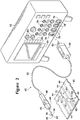
- FIG. 2 is a perspective view of a current probe 40 for use with an oscilloscope 42 having an input by-pass circuit for selectively coupling a current signal from a current carrying conductor 44 to a current sensing circuit in the current probe 40.
- the current probe 40 has a probe body 46, an attachable adapter 48, a control box 50 and a conductive cable 52 coupling the probe body 46 to the control box 50.
- the adapter 48 has a housing 54 from which extends electrically conductive leads 56 and 58.
- Various types of electrical contacts 60, 62 are provided on the electrically conductive leads 56 and 58 of the current probe adapter 48.
- the electrical contacts are adapted for electrically coupling across a non-conductive gap 64 formed in the current carrying conductors 44, such as a circuit trace formed on a circuit board 66 or the like.
- the electrical contacts 60 and 62 are electrically conductive sockets for engaging square pins 68 that are mounted on current carrying conductor 44 on either side of the non-conductive gap 64.
- An electrical jumper 70 is positioned in the square pins 68 for coupling the current signal across the non-conductive gap 64 when the current probe adapter 48 is not coupled to the current carrying conductor 44.
- the electrical contacts are contact pads that are electrically coupled to contacts pads 72 formed on the current carrying conductor 44 on either side of the non-conductive gap 64.
- a removable electrical conductive foil 74 is secured to the contact pads 72 for coupling the current signal across the non-conductive gap 64.
- the electrically conductive foil 72 is removed from the current carrying conductor 44 when the electrically conductive leads 56 and 58 of the adapter 48 are coupled to the current carrying conductor 44.
- the conductive cable 52 has various electrical lines for coupling an output signal from a current sensing circuit disposed in the probe body 46 to the control box 50, and coupling electrical power and communications signals to current sensing circuit and the input by-pass circuit disposed in the current probe body 46.
- the current probe control box 50 is coupled to one of a number of input signal channels 76 of the oscilloscope 42. Each input signal channels 76 has a receptacle interface 78 with each interface having electrically conductive contacts and a coaxial signal jack.
- the current probe control box 50 has an plug interface 80 that mates with the receptacle interfaces 78 and has electrical contacts and a coaxial signal jack that interface with the corresponding electrical contacts and coaxial signal jack in receptacle interfaces 78.
- the interfaces 78 and 80 provide electrical power to the current probe 40 as well as providing communications between the current probe 40 and the oscilloscope 42.
- the interfaces 78 and 80 also provide a signal path between the current probe 40 and the oscilloscope 42.
- the oscilloscope 42 has a display device 82, such as a liquid crystal display, cathode ray tube or the like, and buttons and knobs 84 for controlling the functions of the oscilloscope 42
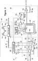
- the input by-pass circuit 90 has a switching circuit 92 coupled between circuit probe inputs 94 and 96 and a current sensing circuit 98.
- the current probe inputs 94 and 96 are coupled to the current carrying conductor 44 via the electrically conductive leads 56 and 58 in the adapter 48.
- a switch control circuit 100 is coupled to the switching circuit 92 for providing switching signal for coupling and decoupling the current probe inputs 94 and 96 from the current sensing circuit 98 without disrupting the current flowing the in the current carrying conductor 44.
- the switching circuit has first and second switches 102 and 104 with each switch 102 and 104 having a terminal 106, 108 coupled to one of the current probe inputs 94, 96.
- Each switch 102 and 104 has a second terminal 110, 112 coupled to a first input 114 of the current sensing circuit 98.
- Each switch 102 and 104 has a third terminal 116, 118 coupled to the other of the current probe inputs 94, 96 and a second input 120 of the current sensing circuit 98.
- Each switch 102 and 104 has an armature 122, 124 that selectively couples the first switch terminal 106,108 to one or the other of the second and third switch terminals 110, 112, 116, 118.
- the first and second switches 102 and 104 are magnetic latch relays that receive activations signals from the switch control circuit 100.
- the activation signals are coupled via buffers 130, 132, 134, and 136 from a serial-to-parallel I/O expander 138.
- the serial-to-parallel I/O expander receives serial data and a clock signal via a serial bus 140, such as an I 2 C bus, SPI bus or the like disposed in the conductive cable 52.
- the serial data and clock are generated by a controller 142 disposed in the current probe control box 50.
- the control box 50 has push-button contact switches 144 and 146 mounted thereon and electrically coupled to signal lines 148 and 150 coupled to inputs on the controller 142.
- the controller 142 has a further serial bus 152 for communicating with the oscilloscope 42.
- the inputs 114 and 120 of the current sensing circuit are coupled to opposing ends of a primary winding 160 wrapped around a magnetic core 162 of a transformer 164.
- the transformer 164 has a secondary winding 166 wrapped around the magnetic core 162 with one end of the secondary winding 166 coupled to electrical ground and the other end coupled to the inverting input of a transimpedance amplifier 168.
- the magnetic core 162 has a Hall effect device 170 disposed therein that is substantially perpendicular to the lines of flux in the magnetic core 120.
- the Hall effect device 170 has a first pair of terminals coupled between a bias source 172 and ground and a second pair of terminals connected to inputs of a differential amplifier 174.
- the single ended output of the differential amplifier 174 is coupled to the non-inverting input of the transimpedance amplifier 168 via a degaussing switch 176.
- the degaussing switch 176 has a first terminal 178 coupled to the output of the differential amplifier 174, a second terminal 180 coupled to the non-inverting input of the transimpedance amplifier 168, and a third terminal 182 coupled to receive a degaussing signal.
- An armature 184 selectively couples the output of the differential amplifier 174 or the degaussing signal to the non-inverting input of the transimpedance amplifier 168.
- the inverting input and output of the transimpedance amplifier 168 are coupled together via a current signal path 186 having a transimpedance resistor 188. Offset control signals may also be applied to the differential amplifier 174 via an offset voltage line 190.
- the current flowing through the current carrying conductor 44 may at times exceed the current rating of the current probe 40 causing the magnetic core 162 of the transformer 164 to saturate. If a user knows when this condition may occur, the switching circuit 92 can be activated to decouple and bypass the primary winding 160 of transformer 164 from the inputs 94 and 96.
- One of the push-button contact switches 144 and 146 is designated for this purpose and is pressed by the user.
- the switches 144, 146 are coupled to electrical ground which initiates logic low signals to the controller 142. Alternately, the switches 144, 146 may be coupled to a voltage source which initiates logic high signals to the controller 142. In the current example, switch 144 is pressed which generates a logic low to the controller 142.
- the logic signal causes the controller 142 to generate serial data indicating that switch 142 has been pressed which is coupled via the serial bus 152 to the oscilloscope 12.
- the oscilloscope 12 generates serial data commands back to the controller 142 to activate the switching circuit 92.
- the oscilloscope 12 may cause an icon to be generates on the oscilloscope display 82 indicating that the input by-pass circuit 90 is activated.
- the controller 142 generates serial data commands that are coupled to the I/O expander 138 via the serial bus 140.
- the I/O expander 138 converts the serial data commands into parallel data that are applied to output pins on the I/O expander 138.
- the parallel data consists of high and low logic levels that cause the armatures 122 and 124 of switches 102 and 104 to change positions.
- the armatures 122 and 124 are positioned to couple the current signal from the current carrying conductor 44 to the primary winding 160 of transformer 162.
- the controller 142 outputs a first serial data command that results in a parallel output signal from the I/O expander 138 having a logic high and logic low one across one of the relays of switches 102, 104, such as switch 102. This causes the armature 122 to switch from contact 110 to contact 116 and short the current signal across the primary winding 160.
- the controller 142 outputs a second serial command that results in a parallel output signal from the I/O expander 138 having a logic high and logic low across the other switch 104. This causes the armature 124 to switch from contact 112 to contact 118 and decouple the primary winding 160 from the inputs 94 and 96. In the preferred embodiment, there is a delay between the first and second serial data commands from the controller 142 to make sure the current signal is being shorted between the inputs 94 and 96 prior to the primary winding 160 being decoupled from the inputs 94 and 96. This assures that there is no disruption of the current signal flowing in the current carrying conductor 44.
- the logic low signal generated by switch 142 may be interpreted directly by the controller 142 which generates the serial data commands to the I/O expander 138.
- the controller 142 may also generate serial data commands to the oscilloscope 42 for generating the icon on the oscilloscope display 82 indicating that the input by-pass circuit 90 is activated.
- a decreasing signal is applied to the secondary winding 166 of the transformer 164.
- the degaussing signal induces a current in the primary winding 160 that is coupled on the current carrying conductor 44.
- the signal may cause damage to circuitry coupled to the current carrying conductor 44.
- an incorrect DC offset may be generated as a result of the degaussing process if the current carrying conductor 44 is coupling a current signal to the primary winding 160 of the transformer 164.
- the current probe should not be electrically coupled to the current carrying conductor 44 during degaussing of the current probe 40.
- the current carrying conductor which acts as the primary winding of the transformer is removed from the transformer.
- the presently described current probe 40 does not use the current carrying conductor 44 as the primary winding but has a separate primary winding 160 electrically coupled to the current carrying conductor 44.
- the switching circuit 92 allows the current probe 40 to remain coupled to the current carrying conductor 44 during the degaussing of the probe 40.
- the other of the push-button contact switches 144 and 146 is designated for degaussing the probe and is pressed by the user.
- the switch 144, 146 initiates a logic signal to the controller 142.
- the logic signal is interpreted by the controller 142 as a degaussing command which generates serial data commands that are coupled to the I/O expander 138 via the serial bus 140.
- the I/O expander 138 converts the serial data commands into parallel data that are applied to output pins on the I/O expander 138.
- the parallel data consists of high and low logic levels that cause the armatures 122 and 124 of switches 102 and 104 to change positions as previously described.
- a further serial data command is sent that results in a logic high being generated by the I/O expander 138 that is coupled to the degaussing switch 176.
- the degaussing switch responds to the logic high signal by coupling the degaussing signal to the non-inverting input of the transimpedance amplifier 168.
- the transimpedance amplifier responds by generating a degaussing voltage signal on the output of the transimpedance amplifier 168.
- the voltage output causes a decreasing current signal to be generated through the current signal path 186.
- the decreasing current signal is coupled to the secondary winding 166 of transformer 164 to degauss the transformer 164.
- the controller 142 may also generate serial data commands to the oscilloscope 42 for generating an icon on the oscilloscope display 82 indicating that the current probe 40 is being degaussed. After the current probe 40 is degaussed, the controller 142 issues a further set of serial data commands that causes the switches 102, 104 and 176 to deactivate so as to re-couple the inputs 94 and 96 to the current sensing circuit 98 and coupled the output of the differential amplifier 174 to the non-inverting input of the transimpedance amplifier 168.
- FIG. 4 there is shown a further embodiment of the input by-pass circuit 90.
- the magnetic latch relays used for the first and second switches 102 and 104 in the previous embodiment are replaced with mechanical switches 200 and 202.
- the mechanical switches 200 and 202 are single-pole-double-throw switches.
- the mechanical switches 200 and 202 have respective terminals 106, 110, 116 and 108, 112, 118 coupled in the same manner as the switches 102 and 104.
- the armature 122 of switch 200 is mechanically coupled to an actuator 204 extending from the probe body 46.
- the armature 124 of switch 202 is mechanically coupled to an actuator 206 extending on the probe body 46.
- the actuators 204 and 206 may be slide actuators, push-button actuators or rotatable actuators with the actuators 202 and 204 bring ganged together so that operating the actuators causes the switching of one of the armatures 122 and then the other armature 124.
- the actuators 204 and 206 function as the switch control 100 in the current implementation.
- the input by-pass circuit 90 using the mechanical switches operates in the similar manner to the input by-pass circuit 90 of Figure 3 .
- the armatures 122 and 124 are shown positioned to couple the current probe inputs 94 and 96 to the current sensing circuit 98. Moving the actuator 204 of switch 200 causes the armature 122 to switch from contact 110 to contact 116 and shorts current probe inputs 94 and 96 together.
- Moving the actuator 206 of switch 202 causes the armature 124 to switch from contact 112 to contact 118 and decouples the current sensing circuit 90 from the inputs 94 and 96.
- the actuators 204 and 206 are mechanically configured to provide delay between the switching of the armatures 122 and 124.
- the mechanical switches 200 and 202 are double-pole-double-throw devices.
- Switch 200 has a second set of terminals 208, 210 and 212 with terminal 208 coupled to electrical ground, terminal 210 left open and terminal 212 coupled to a voltage source via a light emitting diode 214 mounted to the probe body 46.
- An armature 216 selectively couples terminal 208 to terminals 210 and 212 and is activated by the actuator 204.
- Switch 202 has a second set of terminals 218, 222 and 224 with terminal 218 coupled to a signal line 220, terminal 222 coupled to ground and terminals 224 coupled to a voltage source.
- An armature 226 selectively couples the terminal 218 to terminals 222 and 224 and is activated by actuator 206.
- the use of the double-pole-double-throw mechanical switches 200 and 202 allows the use of circuitry for indicating when the input by-pass circuit 90 is active.
- the actuator 216 completes a circuit activating the light emitting diode to give an indication that the input by-pass circuit 90 is active.
- the actuator 226 couples an active high logic level to the signal line 220 which is coupled to the controller 142.
- the controller 142 initiates a serial data command signal to the oscilloscope 42 via the serial bus152 which causes the oscilloscope to generate an indication on the display device 82 that the input by-pass circuit is active.
- the indicating configurations is used with implementation.
Landscapes
- Physics & Mathematics (AREA)
- General Physics & Mathematics (AREA)
- Measuring Instrument Details And Bridges, And Automatic Balancing Devices (AREA)
- Measurement Of Current Or Voltage (AREA)
- Measuring Leads Or Probes (AREA)
- Tests Of Electronic Circuits (AREA)
Description
- The present invention relates generally to current probes and more particularly to a input by-pass circuit for a current probe.
- Current probes used with oscilloscopes apply transformer technology to measure current flowing in a conductor.
Figure 1 illustrates acurrent probe 10 for measuring current signal down toDC having transformer 12 with a ring-shapedmagnetic core 14 defining anaperture 16. The ring-shapedmagnetic core 14 is preferably a split core design where one side of the magnetic core is movable relative to the other sides. This allows a current carryingconductor 18 to be passed through theaperture 16 of thetransformer 12 without having to disconnect the current carryingconductor 18 from a circuit. The current carryingconductor 18 is passed through the aperture in themagnetic core 14 and acts as the primary winding of thetransformer 12. Asecondary winding 20 is wrapped around one side of themagnetic core 14. To allow thecurrent probe 10 to sense DC and low frequency current signals, aHall effect device 22 is positioned in themagnetic core 14 such that the magnetic flux in the magnetic core is substantially perpendicular to theHall effect device 22. Abias source 24 is applied to theHall device 22 and the resulting voltage generated by the Hall effect due to the flux in themagnetic core 14 is coupled to the input of andifferential amplifier 26. The single ended output of thedifferential amplifier 26 is coupled via aswitch 28 to apower amplifier 30. Theswitch 28 is also coupled to receive a degaussing signal that is selectively applied to thetransformer 12. Thepower amplifier 30 generates a current output proportional to the voltage generated by theHall effect device 22. Thepower amplifier 30 is coupled to one side of asecondary winding 20 with the other side of the winding coupled to atransformer termination resistor 32 andvoltage amplifier 34. - The current flowing in the
current carrying conductor 18 induces a magnetic flux that is linked to themagnetic core 14 and thesecondary winding 20. The magnetic flux caused by DC to low frequency current signal is coupled in themagnetic core 14 to theHall effect device 22. TheHall effect device 22 generates a differential voltage that is coupled to the inputs of thedifferential amplifier 26. The output of thedifferential amplifier 26 is coupled throughswitch 28 to thepower amplifier 30. Thepower amplifier 30 generates a current output that is coupled to thesecondary winding 20 of thetransformer 12. The current applied by the power amplifier is in a direction that nulls the flux in themagnetic core 14 caused by the DC to low frequency current signal in thecurrent carrying conductor 18. Higher frequency current signals induce a current in the secondary winding that produces a magnetic flux that is opposite to that generated by the current flowing in the current carryingconductor 18. The current generate by thepower amplifier 20 for DC to low frequency current signals and the current induced into thesecondary winding 20 at higher current frequency signals are summed by thetransformer termination resistor 32 which provides a voltage input to theamplifier 34. The voltage output of theamplifier 34 is a measure of the AC and DC components of the magnetic core flux.U.S. patents 3,525,041 ,5,477,135 and5,493,211 describe the concepts of the abovecurrent probe 10. - In order for a user to degauss the above described current probe, the current carrying
conductor 18 needs to be removed from thecurrent probe 10 otherwise the degaussing signal will induce a current into thecurrent carrying conductor 18 that could damage circuitry in the device under test. Additionally, the user needs to remove thecurrent carrying conductor 18 from thecurrent probe 10 if a sufficiently high current is flowing in the current carryingconductor 18 that would saturate themagnetic core 14 of thetransformer 12. - What is needed in a current probe is a circuit that allows a user to keep the current probe attached to a current carrying conductor while degaussing the current probe or when a current signal is present that would saturate the magnetic core of the transformer. Additionally, the current probe circuit should allow a user the capability to set an offset voltage for the current probe without removing the current probe from the current carrying conductor.
- Document
JP 04 296664 - There is provided a current probe as set out in claim 1.
- Accordingly, the above needs are met with an input by-pass circuit for current probes. The current probe has inputs coupled to a current sensing circuit for receiving a current signal from a device under test with the input by-pass circuit having a switching circuit coupled between the current probe inputs and the current sensing circuit. A switch control is coupled to the switching circuit for selectively coupling and decoupling the current probe inputs to the current sensing circuit such that the current signal continuously flows in the device under test.
- Each of the first and second switches has a common terminal coupled to one of the current probe inputs, a first terminal coupled to the current sensing circuit and a second terminal coupled to the other current probe input. The first and second switches couple the current signal to the current sensing circuit when the common switch terminals of the first and second switches are coupled to the first terminals of the first and second switches. The first and second switches couple the current signal between the current probe inputs when the common switch terminals of the first and second switches are coupled to the second terminals of the first and second switches.
- The first and second switches of the input by-pass circuit may be implemented with magnetic-latch relays or mechanical switches. When the switches are magnetic latch relays, the switch control has at least a first activation switch generating a signal to a controller to initiate the generation of generating command signals coupled to a serial-to-parallel I/O expander. The serial-to-parallel I/O expander generates parallel output data for selectively coupling and decoupling the current probe inputs from the current sensing circuit with one of the command signals delaying one of the first and second switches with respect to the other. The switch control may also have a second activation switch generating a signal to a controller for initiating the generation of command signals coupled to a serial-to-parallel I/O expander. The serial-to-parallel I/O expander generates parallel output data for selectively decoupling the current probe inputs from the current sensing circuit with one of the command signals delaying one of the first and second switches with respect to the other and another command signal coupling a degaussing signal to the current sensing circuit.
- When the first and second switches are mechanical switches, the switch control is a first actuator mechanically coupled to the first mechanical switch and a second actuator coupled to the second mechanical switch with the first and second actuators causing the first and second switches to selectively couple and decouple the current probe inputs from the current sensing circuit with the switching of one of the first and second switches being delayed with respect to the other.
- The objects, advantages and novel features of the present invention are apparent from the following detailed description when read in conjunction with appended claims and attached drawings.
-
-
Figure 1 is a schematic representation of a current probe using a current carrying conductor as a primary transformer winding. -
Figure 2 is a perspective view of a current probe incorporating the input by-pass circuit according to the present invention. -
Figure 3 is schematic representation illustrating a first embodiment of the input by-pass circuit according to the present invention. -
Figure 4 is a schematic representation illustrating a further embodiment of the input by-pass circuit according to the present invention. -
Figure 2 is a perspective view of acurrent probe 40 for use with anoscilloscope 42 having an input by-pass circuit for selectively coupling a current signal from acurrent carrying conductor 44 to a current sensing circuit in thecurrent probe 40. Thecurrent probe 40 has aprobe body 46, anattachable adapter 48, acontrol box 50 and aconductive cable 52 coupling theprobe body 46 to thecontrol box 50. Theadapter 48 has ahousing 54 from which extends electricallyconductive leads electrical contacts conductive leads current probe adapter 48. The electrical contacts are adapted for electrically coupling across anon-conductive gap 64 formed in the current carryingconductors 44, such as a circuit trace formed on acircuit board 66 or the like. In one instance, theelectrical contacts square pins 68 that are mounted on current carryingconductor 44 on either side of thenon-conductive gap 64. An electrical jumper 70 is positioned in thesquare pins 68 for coupling the current signal across thenon-conductive gap 64 when thecurrent probe adapter 48 is not coupled to thecurrent carrying conductor 44. In another instance, the electrical contacts are contact pads that are electrically coupled tocontacts pads 72 formed on the current carryingconductor 44 on either side of thenon-conductive gap 64. A removable electricalconductive foil 74 is secured to thecontact pads 72 for coupling the current signal across thenon-conductive gap 64. The electricallyconductive foil 72 is removed from the current carryingconductor 44 when the electrically conductive leads 56 and 58 of theadapter 48 are coupled to the current carryingconductor 44. - The
conductive cable 52 has various electrical lines for coupling an output signal from a current sensing circuit disposed in theprobe body 46 to thecontrol box 50, and coupling electrical power and communications signals to current sensing circuit and the input by-pass circuit disposed in thecurrent probe body 46. The currentprobe control box 50 is coupled to one of a number ofinput signal channels 76 of theoscilloscope 42. Eachinput signal channels 76 has areceptacle interface 78 with each interface having electrically conductive contacts and a coaxial signal jack. The currentprobe control box 50 has anplug interface 80 that mates with thereceptacle interfaces 78 and has electrical contacts and a coaxial signal jack that interface with the corresponding electrical contacts and coaxial signal jack inreceptacle interfaces 78. Theinterfaces current probe 40 as well as providing communications between thecurrent probe 40 and theoscilloscope 42. Theinterfaces current probe 40 and theoscilloscope 42. Theoscilloscope 42 has a display device 82, such as a liquid crystal display, cathode ray tube or the like, and buttons andknobs 84 for controlling the functions of theoscilloscope 42 - Referring to
Figure 3 , there is shown a representative schematic of the circuitry in thecurrent probe body 46 implementing the input by-pass circuit 90. The input by-pass circuit 90 has a switchingcircuit 92 coupled betweencircuit probe inputs current sensing circuit 98. Thecurrent probe inputs conductor 44 via the electrically conductive leads 56 and 58 in theadapter 48. Aswitch control circuit 100 is coupled to the switchingcircuit 92 for providing switching signal for coupling and decoupling thecurrent probe inputs current sensing circuit 98 without disrupting the current flowing the in the current carryingconductor 44. - The switching circuit has first and
second switches switch current probe inputs switch second terminal first input 114 of thecurrent sensing circuit 98. Eachswitch third terminal current probe inputs second input 120 of thecurrent sensing circuit 98. Eachswitch armature third switch terminals - In the preferred embodiment, the first and
second switches switch control circuit 100. The activation signals are coupled viabuffers O expander 138. The serial-to-parallel I/O expander receives serial data and a clock signal via aserial bus 140, such as an I2C bus, SPI bus or the like disposed in theconductive cable 52. The serial data and clock are generated by acontroller 142 disposed in the currentprobe control box 50. Thecontrol box 50 has push-button contact switches 144 and 146 mounted thereon and electrically coupled to signallines controller 142. Thecontroller 142 has a furtherserial bus 152 for communicating with theoscilloscope 42. - The
inputs magnetic core 162 of atransformer 164. Thetransformer 164 has a secondary winding 166 wrapped around themagnetic core 162 with one end of the secondary winding 166 coupled to electrical ground and the other end coupled to the inverting input of atransimpedance amplifier 168. Themagnetic core 162 has aHall effect device 170 disposed therein that is substantially perpendicular to the lines of flux in themagnetic core 120. TheHall effect device 170 has a first pair of terminals coupled between abias source 172 and ground and a second pair of terminals connected to inputs of adifferential amplifier 174. The single ended output of thedifferential amplifier 174 is coupled to the non-inverting input of thetransimpedance amplifier 168 via adegaussing switch 176. Thedegaussing switch 176 has afirst terminal 178 coupled to the output of thedifferential amplifier 174, asecond terminal 180 coupled to the non-inverting input of thetransimpedance amplifier 168, and a third terminal 182 coupled to receive a degaussing signal. Anarmature 184 selectively couples the output of thedifferential amplifier 174 or the degaussing signal to the non-inverting input of thetransimpedance amplifier 168. The inverting input and output of thetransimpedance amplifier 168 are coupled together via acurrent signal path 186 having atransimpedance resistor 188. Offset control signals may also be applied to thedifferential amplifier 174 via an offsetvoltage line 190. - The current flowing through the current carrying
conductor 44 may at times exceed the current rating of thecurrent probe 40 causing themagnetic core 162 of thetransformer 164 to saturate. If a user knows when this condition may occur, the switchingcircuit 92 can be activated to decouple and bypass the primary winding 160 oftransformer 164 from theinputs switches controller 142. Alternately, theswitches controller 142. In the current example, switch 144 is pressed which generates a logic low to thecontroller 142. In the preferred embodiment, the logic signal causes thecontroller 142 to generate serial data indicating thatswitch 142 has been pressed which is coupled via theserial bus 152 to theoscilloscope 12. Theoscilloscope 12 generates serial data commands back to thecontroller 142 to activate the switchingcircuit 92. Theoscilloscope 12 may cause an icon to be generates on the oscilloscope display 82 indicating that the input by-pass circuit 90 is activated. Thecontroller 142 generates serial data commands that are coupled to the I/O expander 138 via theserial bus 140. The I/O expander 138 converts the serial data commands into parallel data that are applied to output pins on the I/O expander 138. The parallel data consists of high and low logic levels that cause thearmatures switches Figure 3 , thearmatures conductor 44 to the primary winding 160 oftransformer 162. Thecontroller 142 outputs a first serial data command that results in a parallel output signal from the I/O expander 138 having a logic high and logic low one across one of the relays ofswitches switch 102. This causes thearmature 122 to switch fromcontact 110 to contact 116 and short the current signal across the primary winding 160. Thecontroller 142 outputs a second serial command that results in a parallel output signal from the I/O expander 138 having a logic high and logic low across theother switch 104. This causes thearmature 124 to switch fromcontact 112 to contact 118 and decouple the primary winding 160 from theinputs controller 142 to make sure the current signal is being shorted between theinputs inputs conductor 44. Alternately, the logic low signal generated byswitch 142 may be interpreted directly by thecontroller 142 which generates the serial data commands to the I/O expander 138. Thecontroller 142 may also generate serial data commands to theoscilloscope 42 for generating the icon on the oscilloscope display 82 indicating that the input by-pass circuit 90 is activated. - When degaussing the
current probe 40, a decreasing signal is applied to the secondary winding 166 of thetransformer 164. The degaussing signal induces a current in the primary winding 160 that is coupled on the current carryingconductor 44. The signal may cause damage to circuitry coupled to the current carryingconductor 44. Additionally, an incorrect DC offset may be generated as a result of the degaussing process if the current carryingconductor 44 is coupling a current signal to the primary winding 160 of thetransformer 164. For this reason, the current probe should not be electrically coupled to the current carryingconductor 44 during degaussing of thecurrent probe 40. In prior art current probes, the current carrying conductor, which acts as the primary winding of the transformer is removed from the transformer. The presently describedcurrent probe 40 does not use the current carryingconductor 44 as the primary winding but has a separate primary winding 160 electrically coupled to the current carryingconductor 44. The switchingcircuit 92 allows thecurrent probe 40 to remain coupled to the current carryingconductor 44 during the degaussing of theprobe 40. - The other of the push-button contact switches 144 and 146 is designated for degaussing the probe and is pressed by the user. The
switch controller 142. The logic signal is interpreted by thecontroller 142 as a degaussing command which generates serial data commands that are coupled to the I/O expander 138 via theserial bus 140. The I/O expander 138 converts the serial data commands into parallel data that are applied to output pins on the I/O expander 138. The parallel data consists of high and low logic levels that cause thearmatures switches O expander 138 that is coupled to thedegaussing switch 176. The degaussing switch responds to the logic high signal by coupling the degaussing signal to the non-inverting input of thetransimpedance amplifier 168. The transimpedance amplifier responds by generating a degaussing voltage signal on the output of thetransimpedance amplifier 168. The voltage output causes a decreasing current signal to be generated through thecurrent signal path 186. The decreasing current signal is coupled to the secondary winding 166 oftransformer 164 to degauss thetransformer 164. Thecontroller 142 may also generate serial data commands to theoscilloscope 42 for generating an icon on the oscilloscope display 82 indicating that thecurrent probe 40 is being degaussed. After thecurrent probe 40 is degaussed, thecontroller 142 issues a further set of serial data commands that causes theswitches inputs current sensing circuit 98 and coupled the output of thedifferential amplifier 174 to the non-inverting input of thetransimpedance amplifier 168. - Referring to
Figure 4 , there is shown a further embodiment of the input by-pass circuit 90. Like elements fromFigure 3 are labeled the same inFigure 4 . The magnetic latch relays used for the first andsecond switches mechanical switches mechanical switches mechanical switches respective terminals switches armature 122 ofswitch 200 is mechanically coupled to anactuator 204 extending from theprobe body 46. Thearmature 124 ofswitch 202 is mechanically coupled to anactuator 206 extending on theprobe body 46. Theactuators actuators armatures 122 and then theother armature 124. Theactuators switch control 100 in the current implementation. The input by-pass circuit 90 using the mechanical switches operates in the similar manner to the input by-pass circuit 90 ofFigure 3 . Thearmatures current probe inputs current sensing circuit 98. Moving theactuator 204 ofswitch 200 causes thearmature 122 to switch fromcontact 110 to contact 116 and shortscurrent probe inputs actuator 206 ofswitch 202 causes thearmature 124 to switch fromcontact 112 to contact 118 and decouples thecurrent sensing circuit 90 from theinputs actuators armatures - In another implementation, the
mechanical switches Switch 200 has a second set ofterminals terminal 208 coupled to electrical ground,terminal 210 left open and terminal 212 coupled to a voltage source via alight emitting diode 214 mounted to theprobe body 46. Anarmature 216 selectively couples terminal 208 toterminals actuator 204.Switch 202 has a second set ofterminals terminal 218 coupled to asignal line 220, terminal 222 coupled to ground andterminals 224 coupled to a voltage source. Anarmature 226 selectively couples the terminal 218 toterminals actuator 206. - The use of the double-pole-double-throw
mechanical switches pass circuit 90 is active. In one instance, theactuator 216 completes a circuit activating the light emitting diode to give an indication that the input by-pass circuit 90 is active. In the other instance, the actuator 226 couples an active high logic level to thesignal line 220 which is coupled to thecontroller 142. Thecontroller 142 initiates a serial data command signal to theoscilloscope 42 via the serial bus152 which causes the oscilloscope to generate an indication on the display device 82 that the input by-pass circuit is active. Generally, one or the other of the indicating configurations is used with implementation. - It will be obvious to those having skill in the art that many changes may be made to the details of the above-described embodiments of this invention without departing from the underlying principles thereof. The scope of the present invention should, therefore, be determined only by the following claims.
Claims (6)
- A current probe (40) comprising:a current sensing circuit (98);inputs (94, 96) for coupling to a device under test to receive a current signal therefrom; andoutputs (114, 120) coupled to the current sensing circuit (98), wherein the current sensing circuit (98) has a transformer (164) with a magnetic core (162) and a primary winding (160) wrapped around said magnetic core, the primary winding having opposing ends coupled to said outputs, characterized in that the current probe further comprises:a switching circuit (92) electrically coupled to the inputs (94, 96) of the current probe and to the outputs (114, 120) coupled to the current sensing circuit (98); anda switch control circuit (100) coupled to the switching circuit (92) and structured to cause the switching circuit (92) to selectively couple and decouple the current probe inputs (94, 96) from the current sensing circuit (98) while the current probe (40) remains in place and such that a current signal can continuously flow in the device under test;wherein the switching circuit (92) comprises first (102) and second (104) switches coupled to one of the current probe inputs (94) of the current probe (40) with each of the first (102) and second (104) switches having a common terminal (106, 108) coupled to the one current probe input (94), a first terminal (110, 112) coupled to the current sensing circuit (98) through one of the outputs (114) and a second terminal (116, 118) coupled to the other current probe input (96) such that the first (102) and second (104) switches couple the current signal to the current sensing circuit (98) when the common switch terminals of the first (102) and second (104) switches are coupled to the first terminals of the first (102) and second (104) switches, and first (102) and second (104) switches couple the current signal between the current probe inputs when the common switch terminals of the first (102) and second (104) switches are coupled to the second terminals of the first (102) and second switches.
- The current probe (40) as recited in claim 1 wherein the first (102) and second (104) switches are relays.
- The current probe (40) as recited in claim 2 wherein the switch control circuit (100) comprises at least a first activation switch for initiating a signal to cause the first (102) and second (104) switches to selectively couple and decouple the current probe inputs from the current sensing circuit (98) with the switching of one of the first (102) and second (104) switches being delayed with respect to the other.
- The current probe (40) as recited in claim 3 wherein the switch control circuit (100) comprises at least a first activation switch generating a signal to a controller (142) for initiating the generation of command signals coupled to a serial-to-parallel I/O expander (138) that generates parallel output data for selectively coupling and decoupling the current probe inputs from the current sensing circuit (98) with one of the command signals delaying one of the first (102) and second (104) switches with respect to the other.
- The current probe (40) as recited in claim 2 wherein the switch control circuit (100) comprises a second activation switch generating a signal to a controller (142) for initiating the generation of command signals coupled to a serial-to-parallel I/O expander that generates parallel output data for selectively decoupling the current probe inputs from the current sensing circuit (98) with one of the command signals delaying one of the first (102) and second (104) switches with respect to the other and another command signal coupling a degaussing signal to the current sensing circuit (98).
- The current probe (40) as recited in claim 1 wherein the first (102) and second (104) switches are mechanical switches and the switch control is a first actuator mechanically coupled to the first mechanical switch and a second actuator coupled to the second mechanical switch.
Applications Claiming Priority (2)
| Application Number | Priority Date | Filing Date | Title |
|---|---|---|---|
| US11/430,394 US7358717B2 (en) | 2006-05-08 | 2006-05-08 | Input by-pass circuit for a current probe |
| PCT/US2007/068280 WO2007133980A2 (en) | 2006-05-08 | 2007-05-04 | Input by-pass circuit for a current probe |
Publications (2)
| Publication Number | Publication Date |
|---|---|
| EP2016431A2 EP2016431A2 (en) | 2009-01-21 |
| EP2016431B1 true EP2016431B1 (en) | 2018-11-14 |
Family
ID=38658679
Family Applications (1)
| Application Number | Title | Priority Date | Filing Date |
|---|---|---|---|
| EP07761915.3A Ceased EP2016431B1 (en) | 2006-05-08 | 2007-05-04 | Input by-pass circuit for a current probe |
Country Status (5)
| Country | Link |
|---|---|
| US (1) | US7358717B2 (en) |
| EP (1) | EP2016431B1 (en) |
| JP (1) | JP4810648B2 (en) |
| CN (1) | CN101438174B (en) |
| WO (1) | WO2007133980A2 (en) |
Families Citing this family (9)
| Publication number | Priority date | Publication date | Assignee | Title |
|---|---|---|---|---|
| DE102008009962A1 (en) * | 2007-12-04 | 2009-06-10 | Rohde & Schwarz Gmbh & Co. Kg | Probe with high accuracy DC voltage measurement |
| CN103884887A (en) * | 2012-12-20 | 2014-06-25 | 北京普源精电科技有限公司 | Isolation circuit having Hall element and oscilloscope of isolation circuit |
| GB2515787B (en) * | 2013-07-04 | 2018-04-18 | Silicon Sensing Systems Ltd | Pickoff transducer wire bond bit detection |
| US9704637B2 (en) * | 2013-07-15 | 2017-07-11 | Texas Instruments Incorporated | Method and apparatus for demagnetizing transformer cores in closed loop magnetic current sensors |
| US9606147B2 (en) * | 2013-09-27 | 2017-03-28 | Ge Aviation Systems Llc | Apparatus for high bandwidth current sensing |
| CN105675070A (en) * | 2016-03-28 | 2016-06-15 | 中国海洋石油总公司 | Irregular Venturi flowmeter and method for measuring gas-liquid phase flow in multiphase flow by utilization of irregular Venturi flowmeter |
| WO2020017276A1 (en) * | 2018-07-17 | 2020-01-23 | 日置電機株式会社 | Current sensor |
| JP7221150B2 (en) * | 2018-07-17 | 2023-02-13 | 日置電機株式会社 | current sensor |
| DE102020107556A1 (en) * | 2019-03-21 | 2020-09-24 | Tektronix, Inc. | SURFACE-MOUNTED DEVICE FOR COUPLING A TESTING AND MEASURING INSTRUMENT TO A COMPONENT TO BE TESTED |
Citations (1)
| Publication number | Priority date | Publication date | Assignee | Title |
|---|---|---|---|---|
| US20030025514A1 (en) * | 2001-07-26 | 2003-02-06 | Benes Michael J. | Multiple range current measurement system with low power dissipation, fast settling time, and low common mode voltage error |
Family Cites Families (27)
| Publication number | Priority date | Publication date | Assignee | Title |
|---|---|---|---|---|
| US1887421A (en) * | 1930-12-11 | 1932-11-08 | Thomas J Newman | Testing device |
| US2871297A (en) * | 1954-03-08 | 1959-01-27 | Itt | 100-line direct-access crossbar telephone switching unit |
| US2929555A (en) * | 1955-04-27 | 1960-03-22 | Emi Ltd | Automatic control mechanism and interpolating devices therefor |
| US3265971A (en) * | 1963-07-11 | 1966-08-09 | Western Electric Co | Apparatus for testing asymmetrically conducting electrical device for opens, shorts, and polarity orientation |
| US3525041A (en) | 1966-08-08 | 1970-08-18 | Tektronix Inc | Magnetic field measuring method and device effective over a wide frequency range |
| US3482163A (en) * | 1967-05-24 | 1969-12-02 | Tektronix Inc | Magnetic signal measuring device including degaussing means |
| US3800214A (en) * | 1972-01-31 | 1974-03-26 | Flynn J O | Apparatus for testing energized and non-energized electrical circuits |
| US4176313A (en) * | 1978-02-24 | 1979-11-27 | Teradyne, Inc. | Analyzing electrical circuit boards |
| US4514619A (en) * | 1982-09-30 | 1985-04-30 | The B. F. Goodrich Company | Indirect current monitoring via voltage and impedance monitoring |
| JPS62202765A (en) * | 1986-03-04 | 1987-09-07 | Nippon Kogaku Kk <Nikon> | Printer |
| DE58903408D1 (en) * | 1989-02-16 | 1993-03-11 | Mania Gmbh | CIRCUIT FOR MEASURING RESISTORS OF TEST UNITS. |
| US5136252A (en) * | 1990-12-17 | 1992-08-04 | At&T Bell Laboratories | Apparatus and methods for evaluating resistive bodies |
| JP2949247B2 (en) * | 1991-03-26 | 1999-09-13 | 横河電機株式会社 | DC / AC electricity meter |
| JPH0714908Y2 (en) * | 1991-10-02 | 1995-04-10 | 日本アビオニクス株式会社 | Oscilloscope probe |
| US5493211A (en) | 1993-07-15 | 1996-02-20 | Tektronix, Inc. | Current probe |
| JP3288836B2 (en) * | 1993-12-03 | 2002-06-04 | 旭電機株式会社 | Electric resistance measuring method and electric resistance measuring device |
| JP2765490B2 (en) * | 1994-10-03 | 1998-06-18 | 日本電気株式会社 | Magnetic field waveform measurement system |
| JP3246309B2 (en) * | 1996-01-19 | 2002-01-15 | 三菱電機株式会社 | Deterioration detection device for zinc oxide arrester |
| US5804979A (en) * | 1997-05-13 | 1998-09-08 | Fluke Corporation | Circuit for measuring in-circuit resistance and current |
| JP2000235048A (en) * | 1999-02-15 | 2000-08-29 | Ricoh Co Ltd | Measuring probe |
| JP2004245845A (en) * | 1999-03-31 | 2004-09-02 | Seiko Epson Corp | Electronics |
| JP3285568B2 (en) * | 1999-05-24 | 2002-05-27 | 日本電産リード株式会社 | Board wiring inspection apparatus and wiring inspection method |
| JP2001153886A (en) * | 1999-11-26 | 2001-06-08 | Mitsubishi Electric Corp | Probe card and test device provided with the same |
| US6737875B2 (en) * | 2000-05-22 | 2004-05-18 | Damerco, Inc. | Method and apparatus for in-circuit impedance measurement |
| US6362632B1 (en) * | 2000-05-24 | 2002-03-26 | Becs Technology, Inc. | Balanced charge pump capacitive material sensor |
| US6870359B1 (en) * | 2001-12-14 | 2005-03-22 | Le Croy Corporation | Self-calibrating electrical test probe |
| US6891438B2 (en) * | 2002-12-12 | 2005-05-10 | Northrop Grumman Corporation | Adaptive active bias compensation technique for power amplifiers |
-
2006
- 2006-05-08 US US11/430,394 patent/US7358717B2/en not_active Expired - Fee Related
-
2007
- 2007-05-04 EP EP07761915.3A patent/EP2016431B1/en not_active Ceased
- 2007-05-04 JP JP2009510108A patent/JP4810648B2/en not_active Expired - Fee Related
- 2007-05-04 CN CN2007800166772A patent/CN101438174B/en not_active Expired - Fee Related
- 2007-05-04 WO PCT/US2007/068280 patent/WO2007133980A2/en not_active Ceased
Patent Citations (1)
| Publication number | Priority date | Publication date | Assignee | Title |
|---|---|---|---|---|
| US20030025514A1 (en) * | 2001-07-26 | 2003-02-06 | Benes Michael J. | Multiple range current measurement system with low power dissipation, fast settling time, and low common mode voltage error |
Also Published As
| Publication number | Publication date |
|---|---|
| JP4810648B2 (en) | 2011-11-09 |
| US20070273361A1 (en) | 2007-11-29 |
| WO2007133980A3 (en) | 2008-01-10 |
| EP2016431A2 (en) | 2009-01-21 |
| JP2009536743A (en) | 2009-10-15 |
| CN101438174A (en) | 2009-05-20 |
| US7358717B2 (en) | 2008-04-15 |
| CN101438174B (en) | 2011-06-29 |
| WO2007133980A2 (en) | 2007-11-22 |
Similar Documents
| Publication | Publication Date | Title |
|---|---|---|
| EP2016427B1 (en) | Current probing system | |
| WO2007133980A2 (en) | Input by-pass circuit for a current probe | |
| CN111819748B (en) | Residual current circuit breaker and arc detection device with freely-assembled and disassembled residual current circuit breaker | |
| CN103022962B (en) | Disconnect and detect the method for the Roger's Paderewski instrument transformer in disconnect | |
| CN102466751B (en) | A kind of current measuring device | |
| WO2023076396A1 (en) | Single package, dual current transformer for load and residual current measurement | |
| WO2007133975A2 (en) | Current probing system | |
| EP2275827B1 (en) | Clamp-on multimeters including a rogowski coil for measuring alternating current in a conductor | |
| WO2007133965A2 (en) | Current probe | |
| CN1083578C (en) | Device for testing protection relay connected with non-magnetic sensor | |
| CN103675550B (en) | General automobile radio and tape player performance test load box | |
| CN112951670B (en) | Circuit breaker with current detection function and communication power supply | |
| JP3669289B2 (en) | Auxiliary device for relay characteristic test | |
| JP4979062B2 (en) | Signal transmission circuit device | |
| CN216528662U (en) | Mutual inductance device and frame-type circuit breaker | |
| WO2021186661A1 (en) | Contactless power sensor device | |
| CN223651335U (en) | A circuit breaker | |
| JP3149925B2 (en) | Circuit board probing method | |
| EP4177612A1 (en) | Accessory for utilization with non-contact electrical detector | |
| JPH06187898A (en) | Circuit breaker | |
| KR20110003974U (en) | Ratio Differential Relay ONE-TOUCH Test Block | |
| JP2002025410A (en) | Multiplex reed relay | |
| JP2017187355A (en) | measuring device | |
| CN117929800A (en) | Electrical performance test system of cable plug-in component | |
| JP2011247833A (en) | Semiconductor characteristic measuring instrument with contact resistance measuring circuit, and probe holding printed board with contact resistance measuring circuit |
Legal Events
| Date | Code | Title | Description |
|---|---|---|---|
| PUAI | Public reference made under article 153(3) epc to a published international application that has entered the european phase |
Free format text: ORIGINAL CODE: 0009012 |
|
| 17P | Request for examination filed |
Effective date: 20081203 |
|
| AK | Designated contracting states |
Kind code of ref document: A2 Designated state(s): DE FR GB IT |
|
| RIN1 | Information on inventor provided before grant (corrected) |
Inventor name: MENDE, MICHAEL J. Inventor name: DANDY, JONATHAN S. Inventor name: SHARP, THOMAS J. Inventor name: STEVENS, KERRY A. |
|
| DAX | Request for extension of the european patent (deleted) | ||
| RBV | Designated contracting states (corrected) |
Designated state(s): DE FR GB IT |
|
| 17Q | First examination report despatched |
Effective date: 20131018 |
|
| RAP1 | Party data changed (applicant data changed or rights of an application transferred) |
Owner name: TEKTRONIX, INC. |
|
| GRAP | Despatch of communication of intention to grant a patent |
Free format text: ORIGINAL CODE: EPIDOSNIGR1 |
|
| INTG | Intention to grant announced |
Effective date: 20180605 |
|
| GRAS | Grant fee paid |
Free format text: ORIGINAL CODE: EPIDOSNIGR3 |
|
| GRAA | (expected) grant |
Free format text: ORIGINAL CODE: 0009210 |
|
| AK | Designated contracting states |
Kind code of ref document: B1 Designated state(s): DE FR GB IT |
|
| REG | Reference to a national code |
Ref country code: GB Ref legal event code: FG4D |
|
| RIN1 | Information on inventor provided before grant (corrected) |
Inventor name: MENDE, MICHAEL J. Inventor name: STEVENS, KERRY A. Inventor name: DANDY, JONATHAN S. Inventor name: SHARP, THOMAS J. |
|
| REG | Reference to a national code |
Ref country code: DE Ref legal event code: R096 Ref document number: 602007056822 Country of ref document: DE |
|
| PG25 | Lapsed in a contracting state [announced via postgrant information from national office to epo] |
Ref country code: IT Free format text: LAPSE BECAUSE OF FAILURE TO SUBMIT A TRANSLATION OF THE DESCRIPTION OR TO PAY THE FEE WITHIN THE PRESCRIBED TIME-LIMIT Effective date: 20181114 |
|
| REG | Reference to a national code |
Ref country code: DE Ref legal event code: R097 Ref document number: 602007056822 Country of ref document: DE |
|
| PLBE | No opposition filed within time limit |
Free format text: ORIGINAL CODE: 0009261 |
|
| STAA | Information on the status of an ep patent application or granted ep patent |
Free format text: STATUS: NO OPPOSITION FILED WITHIN TIME LIMIT |
|
| 26N | No opposition filed |
Effective date: 20190815 |
|
| REG | Reference to a national code |
Ref country code: DE Ref legal event code: R119 Ref document number: 602007056822 Country of ref document: DE |
|
| GBPC | Gb: european patent ceased through non-payment of renewal fee |
Effective date: 20190504 |
|
| PG25 | Lapsed in a contracting state [announced via postgrant information from national office to epo] |
Ref country code: DE Free format text: LAPSE BECAUSE OF NON-PAYMENT OF DUE FEES Effective date: 20191203 Ref country code: GB Free format text: LAPSE BECAUSE OF NON-PAYMENT OF DUE FEES Effective date: 20190504 |
|
| PG25 | Lapsed in a contracting state [announced via postgrant information from national office to epo] |
Ref country code: FR Free format text: LAPSE BECAUSE OF NON-PAYMENT OF DUE FEES Effective date: 20190531 |