EP2015455A2 - D/A converter circuit - Google Patents
D/A converter circuit Download PDFInfo
- Publication number
- EP2015455A2 EP2015455A2 EP08011381A EP08011381A EP2015455A2 EP 2015455 A2 EP2015455 A2 EP 2015455A2 EP 08011381 A EP08011381 A EP 08011381A EP 08011381 A EP08011381 A EP 08011381A EP 2015455 A2 EP2015455 A2 EP 2015455A2
- Authority
- EP
- European Patent Office
- Prior art keywords
- voltages
- resistor string
- analog
- resistor
- resistors
- Prior art date
- Legal status (The legal status is an assumption and is not a legal conclusion. Google has not performed a legal analysis and makes no representation as to the accuracy of the status listed.)
- Granted
Links
Images


Classifications
-
- H—ELECTRICITY
- H03—ELECTRONIC CIRCUITRY
- H03M—CODING; DECODING; CODE CONVERSION IN GENERAL
- H03M1/00—Analogue/digital conversion; Digital/analogue conversion
- H03M1/66—Digital/analogue converters
-
- H—ELECTRICITY
- H03—ELECTRONIC CIRCUITRY
- H03M—CODING; DECODING; CODE CONVERSION IN GENERAL
- H03M1/00—Analogue/digital conversion; Digital/analogue conversion
- H03M1/66—Digital/analogue converters
- H03M1/68—Digital/analogue converters with conversions of different sensitivity, i.e. one conversion relating to the more significant digital bits and another conversion to the less significant bits
- H03M1/682—Digital/analogue converters with conversions of different sensitivity, i.e. one conversion relating to the more significant digital bits and another conversion to the less significant bits both converters being of the unary decoded type
-
- H—ELECTRICITY
- H03—ELECTRONIC CIRCUITRY
- H03M—CODING; DECODING; CODE CONVERSION IN GENERAL
- H03M1/00—Analogue/digital conversion; Digital/analogue conversion
- H03M1/12—Analogue/digital converters
-
- H—ELECTRICITY
- H03—ELECTRONIC CIRCUITRY
- H03M—CODING; DECODING; CODE CONVERSION IN GENERAL
- H03M1/00—Analogue/digital conversion; Digital/analogue conversion
- H03M1/66—Digital/analogue converters
- H03M1/74—Simultaneous conversion
- H03M1/76—Simultaneous conversion using switching tree
- H03M1/765—Simultaneous conversion using switching tree using a single level of switches which are controlled by unary decoded digital signals
Definitions
- This invention relates to a D/A converter circuit using resistor strings.
- An R-2R type D/A converter circuit has been known as a D/A converter circuit using ladder resistors.
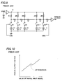
- This type of D/A converter circuit is provided with the R-2R ladder resistors to which a reference voltage VREF is supplied, (n+1) constant current sources each corresponding to each of (n+1) bits (ranging from LSB (Least Significant Bit) to MSB (Most Significant Bit)) in a digital signal, respectively, and (n+1) switches S0-Sn each corresponding to each of the (n+1) bits in the digital signal, respectively, as shown in Fig. 9 , and is capable of converting the (n+1) bit digital signal into an analog signal by turning the switches S0-Sn on/off.
- This type of D/A converter circuit is disclosed in Japanese Patent Application Publication No. H10-135836 .
- a D/A converter circuit using a resistor string as shown in Fig. 11 . It is a nine-bit D/A converter circuit provided with a resistor string composed of 511 serially connected resistors to which a reference voltage VREF is supplied and 512 switches S1-S512 and capable of converting a nine-bit digital signal into an analog signal by turning the switches S1-S512 on/off corresponding to the nine-bit digital signal.
- the bit inversion does not occur in the D/A conversion circuit using the resistor string, there is a problem that it takes a very large layout area (as large as five times of a layout area required by the R-2R type D/A converter circuit in the case of the nine-bit D/A converter circuit).
- the object of this invention is directed to offering a multi-bit (six-bit or more than six-bit) D/A converter circuit that is capable of preventing the bit inversion as well as reducing the layout area.
- This invention offers a D/A converter circuit that converts a digital input signal including a plurality of upper bits and a plurality of lower bits into an analog voltage, having a first resistor string that generates a plurality of first analog voltages, a first switching circuit that selects a pair of first analog voltages out of the plurality of first analog voltages generated by the first resistor string in accordance with the plurality of upper bits, buffers, a second resistor string that is provided with the selected pair of first analog voltages as reference voltages through the buffers and generates a plurality of second analog voltages, and a second switching circuit that selects a pair of second analog voltages out of the plurality of analog voltages generated by the second resistor string in accordance with the plurality of lower bits.
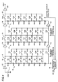
- Fig. 1 shows a structure of a nine-bit D/A converter circuit according to a first embodiment of this invention.
- a first resistor string 10 is composed of eight resistors R1-R8 connected in series.
- a reference voltage VREF generated by a reference voltage source 11 is supplied to an end of the resistor R1 through a buffer 12.
- An end of the resistor R8 is grounded.
- the resistors R1-R8 have the same resistance as the others so that the nine analog voltages increase by a constant increment.
- a first switching circuit 13 is provided in order to select a pair of analog voltages generated across one of the resistors R1-R8 in the first resistor string 10.
- the first switching circuit 13 is composed of 16 switches S1-S16.
- a decoder circuit 14 decodes values of upper three bits (D8, D7, D6) in a nine-bit input digital signal D0-D8 to generate signals to control the first switching circuit 13.
- Table 1 shows correlation between the values of the upper three bits (D8, D7, D6) and the switches turned on accordingly.
- Each of the pair of analog voltages across the resistor selected by the first switching circuit 13 is provided to each end of a second resistor string 17 through each of buffers 15 and 16 as a reference voltage, respectively.
- Each of the buffers 15 and 16 is composed of an operational amplifier having high input impedance and low output impedance, for example.
- the second resistor string 17 is composed of eight resistors R9-R16 connected in series, there are generated nine analog voltages each at each end of the resistors R9-R16 in the second resistor string 17. It is preferable that the resistors R9-R16 have the same resistance as the others so that the nine analog voltages increase by a constant increment.
- a second switching circuit 18 is provided in order to select a pair of analog voltages generated across one of the resistors R9-R16 in the second resistor string 17.
- the second switching circuit 18 is composed of 16 switches S17-S32.
- the decoder circuit 14 decodes values of middle three bits (D5, D4, D3) in the nine-bit digital input signal D0-D8 to generate signals to control the second switching circuit 18.
- Table 2 shows correlation between the values of the middle three bits (D5, D4, D3) and the switches turned on accordingly.
- Each of the pair of analog voltages across the resistor selected by the second switching circuit 18 is provided to each end of a third resistor string 21 through each of buffers 19 and 20 as a reference voltage, respectively.
- Each of the buffers 19 and 20 is composed of an operational amplifier having high input impedance and low output impedance, for example.
- the third resistor string 21 is composed of eight resistors R17-R24 connected in series, there are generated eight analog voltages each at each end of the resistors R17-R24 in the third resistor string 21. It is preferable that the resistors R17-R24 have the same resistance as the others so that the eight analog voltages increase by a constant increment.
- a third switching circuit 22 is provided in order to select one of the eight analog voltages generated in the third resistor string 21.
- the third switching circuit 22 is composed of eight switches S33-S40.
- the decoder circuit 14 decodes values of lower three bits (D2, D1, D0) in the nine-bit digital input signal D0-D8 to generate signals to control the third switching circuit 22.
- Table 3 shows correlation between the values of the lower three bits (D2, D1, D0) and the switches turned on accordingly.
- An analog voltage VOUT selected by the third switching circuit 22 is outputted through a buffer 23. Therefore, the D/A converter circuit can convert the nine-bit digital input signal D0-D8 into 512 different analog voltages. Since the D/A converter circuit is of the resistor string type, it does not cause the bit inversion. In addition, a layout area required by the D/A converter circuit can be reduced because the D/A converter circuit uses three-stage resistor strings and requires only 24 resistors and 40 switches.
- the second resistor string 17 since the pair of analog voltages selected from the voltages generated in the first resistor string 10 is provided to the second resistor string 17 through the buffers 15 and 16 with high input impedance and low output impedance, the second resistor string 17 does not affect the analog voltages generated in the first resistor string 10. Similarly, since the pair of analog voltages selected from the voltages generated in the second resistor string 17 is provided to the third resistor string 21 through the buffers 19 and 20 with high input impedance and low output impedance, the third resistor string 21 does not affect the analog voltages generated in the second resistor string 17.
- the analog voltages generated in the resistor string are provided to the subsequent resistor string through the buffers (buffers 15 and 16, for example) as the reference voltages.
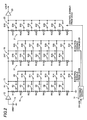
- the buffers 15, 16, 19 and 20 used in the first embodiment are removed and the analog voltages generated in the resistor string are directly provided to the subsequent resistor string as the reference voltages, as shown in Fig. 2 .
- the analog voltages generated in the resistor string are affected and modified by the subsequent resistor string, since the subsequent resistor string is connected with the resistor string in parallel. In return, the analog voltages generated in the subsequent resistor string are also affected.
- a resistance of each of the resistors R9-R16 in the second resistor string 17 is set to be larger than a resistance of each of the resistors R1-R8 in the first resistor string 10.
- a resistance of each of the resistors R17-24 in the third resistor string 21 is set to be larger than the resistance of each of the resistors R9-R16 in the second resistor string 17.
- the resistance of each of the resistors R1-R8 in the first resistor string 10 is set to be 250 ⁇ and that the resistance of each of the resistors R9-R16 in the second resistor string 17 is set to be 10 K ⁇ .
- a voltage V1 at a connecting node between the resistor R1 and the resistor R2 is represented by the following equation.
- V ⁇ 1 7 ⁇ R 7 ⁇ R + Rt ⁇ VREF
- Rt represents a resistance of a parallel combination of a resistance R of the resistor R1 and a resistance 8xR' of the serially connected eight resistors R9-R16 in the second resistor string 17.
- R' denotes a resistance of each of the resistors R9-R16.
- a voltage V1' at the connecting node between the resistor R1 and the resistor R2 is represented by the following equation.
- V ⁇ 1 ⁇ ⁇ 6 ⁇ R + Rt 7 ⁇ R + Rt ⁇ VREF
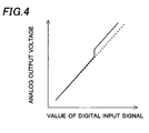
- ⁇ V has a positive value because R > Rt. Therefore, the abrupt change as shown in Fig. 4 is caused when the values of the upper three bits (D8, D7, D6) in the digital signal changes from (1, 1, 0) to (1, 1, 1).
- a D/A converter circuit is provided with an adjusting resistor RH to adjust the abrupt change, which is connected in series with the resistors R9-R16 in the second resistor string 17, as shown in Fig. 5 .
- a resistor R25 is added to the first resistor string 10.
- the first switching circuit 13 is modified so as to select a pair of analog voltages generated at both ends of two serially-connected neighbouring resistors selected from among the resistors R1-R8 and R25.
- Table 4 shows correlation between the values of the upper three bits (D8, D7, D6) and the switches turned on accordingly.
- the switches S1 and S9 are turned on to select the voltages at both ends of the resistors R1 and R2, as shown in Fig. 6A . Then, the selected voltages are provided to the second resistor string 17 as the reference voltages.
- the switches S2 and S10 are turned on to select the voltages at both ends of the resistors R2 and R3, as shown in Fig. 6B . Then, the selected voltages are provided to the second resistor string 17 as the reference voltages.
- the abrupt change described above is similarly caused when a resistance of the adjusting resistor RH is equal to 8xR'. It is preferable to attain an effect of adjustment to reduce the abrupt change that the resistance of the adjusting resistor RH is slightly smaller than 8xR'. According to results of circuit simulations conducted by the inventor, the effect of adjustment appeared to be obtained when the resistance of the adjusting resistor RH was set to be 7.5xR', which is smaller than 8xR' by an amount corresponding to a half of the increment in the digital data.
- a D/A converter circuit In a D/A converter circuit according to a fourth embodiment of this invention, the number of switches is further reduced by modifying the structure of the first switching circuit 13 and the second switching circuit 18 in the D/A converter circuit according to the first embodiment.
- the explanation is given hereafter based on modifications applied to the D/A converter according to the first embodiment, similar modifications may be applied to the D/A converters according to the second and third embodiments.
- a first switching circuit 13A is composed of nine switches S1-S9, and a second switching circuit 18A is also composed of nine switches S10-S18, as shown in Fig. 7 .
- Table 5 shows correlation between the values of the upper three bits (D8, D7, D6) and the switches turned on accordingly, regarding the first switching circuit 13A.
- the bit inversion can be prevented and the layout area can be reduced.
Abstract
Description
- This invention relates to a D/A converter circuit using resistor strings.
- An R-2R type D/A converter circuit has been known as a D/A converter circuit using ladder resistors. This type of D/A converter circuit is provided with the R-2R ladder resistors to which a reference voltage VREF is supplied, (n+1) constant current sources each corresponding to each of (n+1) bits (ranging from LSB (Least Significant Bit) to MSB (Most Significant Bit)) in a digital signal, respectively, and (n+1) switches S0-Sn each corresponding to each of the (n+1) bits in the digital signal, respectively, as shown in
Fig. 9 , and is capable of converting the (n+1) bit digital signal into an analog signal by turning the switches S0-Sn on/off. This type of D/A converter circuit is disclosed in Japanese Patent Application Publication No.H10-135836 - When data of the (n+1) bit digital signal varies, the switches S0-Sn are turned on or off accordingly, and corresponding currents flow from the constant current sources to the R-2R ladder resistors in the circuit described above. At that time, however, there is caused a slight fluctuation in a voltage (the reference voltage VREF) at a node A shown in
Fig. 9 . In addition, there are caused slight variations in ratios among constant currents I0-In drawn from the (n+1) constant current sources that are made of current mirrors. As a result, there is caused a "bit inversion" in a six-bit or more than six-bit D/A converter circuit, as shown inFig. 10 . The bit inversion means a drop in an analog output voltage as a value of the digital signal increases. - Also, there has been known a D/A converter circuit using a resistor string as shown in
Fig. 11 . It is a nine-bit D/A converter circuit provided with a resistor string composed of 511 serially connected resistors to which a reference voltage VREF is supplied and 512 switches S1-S512 and capable of converting a nine-bit digital signal into an analog signal by turning the switches S1-S512 on/off corresponding to the nine-bit digital signal. Although the bit inversion does not occur in the D/A conversion circuit using the resistor string, there is a problem that it takes a very large layout area (as large as five times of a layout area required by the R-2R type D/A converter circuit in the case of the nine-bit D/A converter circuit). - The object of this invention is directed to offering a multi-bit (six-bit or more than six-bit) D/A converter circuit that is capable of preventing the bit inversion as well as reducing the layout area.
- The solution according to the invention resides in the features of the independent claim and preferably in those of the dependent claims. This invention offers a D/A converter circuit that converts a digital input signal including a plurality of upper bits and a plurality of lower bits into an analog voltage, having a first resistor string that generates a plurality of first analog voltages, a first switching circuit that selects a pair of first analog voltages out of the plurality of first analog voltages generated by the first resistor string in accordance with the plurality of upper bits, buffers, a second resistor string that is provided with the selected pair of first analog voltages as reference voltages through the buffers and generates a plurality of second analog voltages, and a second switching circuit that selects a pair of second analog voltages out of the plurality of analog voltages generated by the second resistor string in accordance with the plurality of lower bits.
- With the resistor string type D/A converter circuit described above, reducing a layout area as well as preventing a bit inversion is made possible, because the number of resistors and the number of switches can be reduced.
-
-
Fig. 1 is a circuit diagram showing a structure of a D/A converter circuit according to a first embodiment of this invention. -
Fig. 2 is a circuit diagram showing a structure of a D/A converter circuit according to a second embodiment of this invention. -
Fig. 3 shows the operations of the D/A converter circuit according to the second embodiment of this invention. -
Fig. 4 shows the operations of the D/A converter circuit according to the second embodiment of this invention. -
Fig. 5 is a circuit diagram showing a structure of a D/A converter circuit according to a third embodiment of this invention. -
Figs. 6A and 6B are circuit diagrams showing operations of the D/A converter circuit according to the third embodiment of this invention. -
Fig. 7 is a circuit diagram showing a structure of a D/A converter circuit according to a fourth embodiment of this invention. -
Figs. 8A and 8B are circuit diagrams showing operations of the D/A converter circuit according to the fourth embodiment of this invention. -
Fig. 9 is a circuit diagram showing a structure of a conventional R-2R type D/A converter circuit. -
Fig. 10 shows a bit inversion in the conventional R-2R type D/A converter circuit. -
Fig. 11 is a circuit diagram showing a structure of a conventional resistor string type D/A converter circuit. -
Fig. 1 shows a structure of a nine-bit D/A converter circuit according to a first embodiment of this invention. Afirst resistor string 10 is composed of eight resistors R1-R8 connected in series. A reference voltage VREF generated by areference voltage source 11 is supplied to an end of the resistor R1 through abuffer 12. An end of the resistor R8 is grounded. As a result, there are generated nine analog voltages ranging from 0 to VREF, each at each end of the resistors R1-R8 in thefirst resistor string 10. It is preferable that the resistors R1-R8 have the same resistance as the others so that the nine analog voltages increase by a constant increment. - A
first switching circuit 13 is provided in order to select a pair of analog voltages generated across one of the resistors R1-R8 in thefirst resistor string 10. Thefirst switching circuit 13 is composed of 16 switches S1-S16. Adecoder circuit 14 decodes values of upper three bits (D8, D7, D6) in a nine-bit input digital signal D0-D8 to generate signals to control thefirst switching circuit 13. Table 1 shows correlation between the values of the upper three bits (D8, D7, D6) and the switches turned on accordingly.[Table 1] D8 D7 D6 Switches Turned ON Voltages Selected 0 0 0 S8, S16 Voltages at Both Ends of R8 0 0 1 S7, S15 Voltages at Both Ends of R7 0 1 0 S6, S15 Voltages at Both Ends of R6 0 1 1 S5, S13 Voltages at Both Ends of R5 1 0 0 S4, S12 Voltages at Both Ends of R4 1 0 1 S3, S11 Voltages at Both Ends of R3 1 1 0 S2, S10 Voltages at Both Ends of R2 1 1 1 S1, S9 Voltages at Both Ends of R1 - Each of the pair of analog voltages across the resistor selected by the
first switching circuit 13 is provided to each end of asecond resistor string 17 through each ofbuffers buffers - When the values of the upper three bits (D8, D7, D6) in the digital signal are (1, 1, 0), for example, the switches S2 and S10 are turned on. Analog voltages VREFx6/8 and VREFx7/8 are generated at both ends of the resistor R2. The analog voltage VREFx7/8 is provided to one end of the
second resistor string 17 through the switch S2 and thebuffer 15, while the analog voltage VREFx6/8 is provided to another end of thesecond resistor string 17 through the switch S10 and thebuffer 16. - Since the
second resistor string 17 is composed of eight resistors R9-R16 connected in series, there are generated nine analog voltages each at each end of the resistors R9-R16 in thesecond resistor string 17. It is preferable that the resistors R9-R16 have the same resistance as the others so that the nine analog voltages increase by a constant increment. - A
second switching circuit 18 is provided in order to select a pair of analog voltages generated across one of the resistors R9-R16 in thesecond resistor string 17. Thesecond switching circuit 18 is composed of 16 switches S17-S32. Thedecoder circuit 14 decodes values of middle three bits (D5, D4, D3) in the nine-bit digital input signal D0-D8 to generate signals to control thesecond switching circuit 18. Table 2 shows correlation between the values of the middle three bits (D5, D4, D3) and the switches turned on accordingly.[Table 2] D5 D4 D3 Switches Turned ON Voltages Selected 0 0 0 S24, S32 Voltages at Both Ends of R16 0 0 1 S23, S31 Voltages at Both Ends of R15 0 1 0 S22, S30 Voltages at Both Ends of R14 0 1 1 S21, S29 Voltages at Both Ends of R13 1 0 0 S20, S28 Voltages at Both Ends of R12 1 0 1 S19, S27 Voltages at Both Ends of R11 1 1 0 S18, S26 Voltages at Both Ends of R10 1 1 1 S17, S25 Voltages at Both Ends of R9 - Each of the pair of analog voltages across the resistor selected by the
second switching circuit 18 is provided to each end of athird resistor string 21 through each ofbuffers buffers - When the values of the middle three bits (D5, D4, D3) in the digital signal are (1, 1, 0), for example, the switches S18 and S26 are turned on. Analog voltages VREF'x6/8 and VREF'x7/8 are generated at both ends of the resistor R10. VREF' represents a difference between electric potentials at both ends of the
second resistor string 17. The analog voltage VREF'x7/8 is provided to one end of thethird resistor string 21 through the switch S18 and thebuffer 19, while the analog voltage VREF'x6/8 is provided to another end of thethird resistor string 21 through the switch S19 and thebuffer 20. - Since the
third resistor string 21 is composed of eight resistors R17-R24 connected in series, there are generated eight analog voltages each at each end of the resistors R17-R24 in thethird resistor string 21. It is preferable that the resistors R17-R24 have the same resistance as the others so that the eight analog voltages increase by a constant increment. - A
third switching circuit 22 is provided in order to select one of the eight analog voltages generated in thethird resistor string 21. Thethird switching circuit 22 is composed of eight switches S33-S40. Thedecoder circuit 14 decodes values of lower three bits (D2, D1, D0) in the nine-bit digital input signal D0-D8 to generate signals to control thethird switching circuit 22. Table 3 shows correlation between the values of the lower three bits (D2, D1, D0) and the switches turned on accordingly.[Table 3] D2 D1 D0 Switches Turned ON Voltages Selected 0 0 0 S40 Voltage at Connecting Node R23-R24 0 0 1 S39 Voltage at Connecting Node R22-R23 0 1 0 S38 Voltage at Connecting Node R21-R22 0 1 1 S37 Voltage at Connecting Node R20- R21 1 0 0 S36 Voltage at Connecting Node R19- R20 1 0 1 S35 Voltage at Connecting Node R18- R19 1 1 0 S34 Voltage at Connecting Node R17- R18 1 1 1 S33 Voltage at Upper End of R17 - An analog voltage VOUT selected by the
third switching circuit 22 is outputted through abuffer 23. Therefore, the D/A converter circuit can convert the nine-bit digital input signal D0-D8 into 512 different analog voltages. Since the D/A converter circuit is of the resistor string type, it does not cause the bit inversion. In addition, a layout area required by the D/A converter circuit can be reduced because the D/A converter circuit uses three-stage resistor strings and requires only 24 resistors and 40 switches. - Furthermore, since the pair of analog voltages selected from the voltages generated in the
first resistor string 10 is provided to thesecond resistor string 17 through thebuffers second resistor string 17 does not affect the analog voltages generated in thefirst resistor string 10. Similarly, since the pair of analog voltages selected from the voltages generated in thesecond resistor string 17 is provided to thethird resistor string 21 through thebuffers third resistor string 21 does not affect the analog voltages generated in thesecond resistor string 17. - In the D/A converter circuit according to the first embodiment, the analog voltages generated in the resistor string are provided to the subsequent resistor string through the buffers (buffers 15 and 16, for example) as the reference voltages. When an offset of the buffer is affected by an analog input voltage or by temperature, however, accuracy in the D/A conversion may be degraded. Therefore, in a D/A converter circuit according to a second embodiment of this invention, the
buffers Fig. 2 . However, the analog voltages generated in the resistor string are affected and modified by the subsequent resistor string, since the subsequent resistor string is connected with the resistor string in parallel. In return, the analog voltages generated in the subsequent resistor string are also affected. - Considering the above, a resistance of each of the resistors R9-R16 in the
second resistor string 17 is set to be larger than a resistance of each of the resistors R1-R8 in thefirst resistor string 10. Similarly, a resistance of each of the resistors R17-24 in thethird resistor string 21 is set to be larger than the resistance of each of the resistors R9-R16 in thesecond resistor string 17. For example, it is preferable that the resistance of each of the resistors R1-R8 in thefirst resistor string 10 is set to be 250 Ω and that the resistance of each of the resistors R9-R16 in thesecond resistor string 17 is set to be 10 KΩ. By doing so, the resistor of 250 Ω in thefirst resistor string 10 is connected in parallel with the resistors of 10 KΩ x 8 = 80 KΩ in thesecond resistor string 17, which makes it possible to reduce the modification in the analog voltages substantially. - Even if the structure describe above is adopted, however, there is a problem that an abrupt change is caused in the analog output voltage as the value of the digital input signal increases, as shown in
Fig. 4 . This problem is explained hereafter referring toFigs. 3A, 3B and4 . - When values of the upper three bits (D8, D7, D6) are (1, 1, 1), the switches S1 and S9 are turned on to select the voltages at both ends of the resistor R1, as shown in
Fig. 3A . A voltage V1 at a connecting node between the resistor R1 and the resistor R2 is represented by the following equation.
where Rt represents a resistance of a parallel combination of a resistance R of the resistor R1 and a resistance 8xR' of the serially connected eight resistors R9-R16 in thesecond resistor string 17. R' denotes a resistance of each of the resistors R9-R16. - When the values of the upper three bits (D8, D7, D6) are (1, 1, 0), the switches S2 and S10 are turned on to select the voltages at both ends of the resistor R2, as shown in
Fig. 3B . A voltage V1' at the connecting node between the resistor R1 and the resistor R2 is represented by the following equation.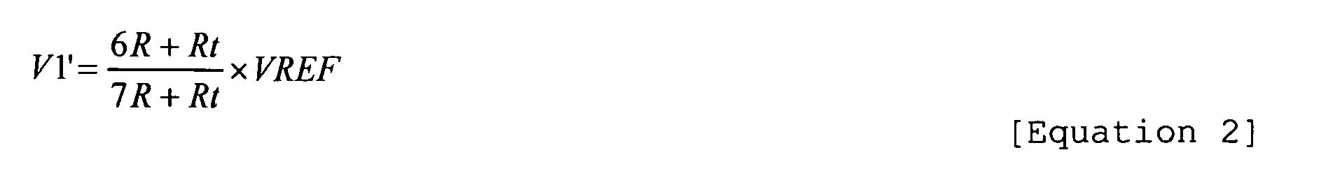
- The voltages V1 and V1' should be equal to each other because they represent the voltage at the same node. In reality, however, there is a voltage difference ΔV represented by the following equation.

- ΔV has a positive value because R > Rt. Therefore, the abrupt change as shown in
Fig. 4 is caused when the values of the upper three bits (D8, D7, D6) in the digital signal changes from (1, 1, 0) to (1, 1, 1). - Considering the above, a D/A converter circuit according to a third embodiment of this invention is provided with an adjusting resistor RH to adjust the abrupt change, which is connected in series with the resistors R9-R16 in the
second resistor string 17, as shown inFig. 5 . - In addition, a resistor R25 is added to the
first resistor string 10. Also, thefirst switching circuit 13 is modified so as to select a pair of analog voltages generated at both ends of two serially-connected neighbouring resistors selected from among the resistors R1-R8 and R25. Table 4 shows correlation between the values of the upper three bits (D8, D7, D6) and the switches turned on accordingly.[Table 4] D8 D7 D6 Switches Turned ON Voltages Selected 0 0 0 S8, S16 Voltages at Both Ends of R8-R25 0 0 1 S7, S15 Voltages at Both Ends of R7-R8 0 1 0 S6, S15 Voltages at Both Ends of R6-R7 0 1 1 S5, S13 Voltages at Both Ends of R5- R6 1 0 0 S4, S12 Voltages at Both Ends of R4- R5 1 0 1 S3, S11 Voltages at Both Ends of R3- R4 1 1 0 S2, S10 Voltages at Both Ends of R2- R3 1 1 1 S1, S9 Voltages at Both Ends of R1-R2 - For example, when the values of the upper three bits (D8, D7, D6) are (1, 1, 1), the switches S1 and S9 are turned on to select the voltages at both ends of the resistors R1 and R2, as shown in
Fig. 6A . Then, the selected voltages are provided to thesecond resistor string 17 as the reference voltages. Also, when the values of the upper three bits (D8, D7, D6) are (1, 1, 0), the switches S2 and S10 are turned on to select the voltages at both ends of the resistors R2 and R3, as shown inFig. 6B . Then, the selected voltages are provided to thesecond resistor string 17 as the reference voltages. - As the resistance of the serially-connected eight resistors R9-R16 in the
second resistor string 17 is 8xR', the abrupt change described above is similarly caused when a resistance of the adjusting resistor RH is equal to 8xR'. It is preferable to attain an effect of adjustment to reduce the abrupt change that the resistance of the adjusting resistor RH is slightly smaller than 8xR'. According to results of circuit simulations conducted by the inventor, the effect of adjustment appeared to be obtained when the resistance of the adjusting resistor RH was set to be 7.5xR', which is smaller than 8xR' by an amount corresponding to a half of the increment in the digital data. - In a D/A converter circuit according to a fourth embodiment of this invention, the number of switches is further reduced by modifying the structure of the
first switching circuit 13 and thesecond switching circuit 18 in the D/A converter circuit according to the first embodiment. Although the explanation is given hereafter based on modifications applied to the D/A converter according to the first embodiment, similar modifications may be applied to the D/A converters according to the second and third embodiments. - A
first switching circuit 13A is composed of nine switches S1-S9, and asecond switching circuit 18A is also composed of nine switches S10-S18, as shown inFig. 7 . Table 5 shows correlation between the values of the upper three bits (D8, D7, D6) and the switches turned on accordingly, regarding thefirst switching circuit 13A.[Table 5] D8 D7 D6 Switches Turned ON Voltages Selected 0 0 0 S8, S9 Voltages at Both Ends of R8 0 0 1 S7, S8 Voltages at Both Ends of R7 0 1 0 S6, S7 Voltages at Both Ends of R6 0 1 1 S5, S6 Voltages at Both Ends of R5 1 0 0 S4, S5 Voltages at Both Ends of R4 1 0 1 S3, S4 Voltages at Both Ends of R3 1 1 0 S2, S3 Voltages at Both Ends of R2 1 1 1 S1, S2 Voltages at Both Ends of R1 - It should be noted that relative heights of reference voltages provided to the
second resistor string 17 are reversed when a pair of voltages across one of even-numbered resistors R2, R4, R6 and R8 is selected. This point is further explained below. When the values of the upper three bits (D8, D7, D6) are (1, 1, 1), the switches S1 and S2 are turned on, as shown inFig. 8A . Then, the voltage VREF at an upper end of the resistor R1 is applied to thebuffer 15 while a voltage 7/8xVREF at a lower end of the resistor R1 is applied to thebuffer 16. - On the other hand, when the values of the upper three bits (D8, D7, D6) are (1, 1, 0), the switches S2 and S3 are turned on, as shown in
Fig. 8B . Then, a voltage 7/8xVREF at an upper end of the resistor R2 is applied to thebuffer 16 while avoltage 6/8xVREF at a lower end of the resistor R2 is applied to thebuffer 15. - When the relative heights of the reference voltages provided to the
second resistor string 17 are reversed as described above, turning on/off of the switches in thesecond switching circuit 18A needs to be modified accordingly. - With the D/A converter circuits (six-bits or more than six-bits) according to the embodiments of this invention, the bit inversion can be prevented and the layout area can be reduced.
Claims (7)
- A D/A converter circuit that converts an input digital signal comprising a plurality of upper bits and a plurality of lower bits into an analog voltage, comprising:- a first resistor string (10) that generates a plurality of first analog voltages;- a first switching circuit (13) that selects a pair of first analog voltages out of the first analog voltages generated by the first resistor string (10) according to the upper bits;- buffers (15, 16);- a second resistor string (17) provided with the pair of first analog voltages as reference voltages through the buffers and generates a plurality of second analog voltages; and- a second switching circuit (18) that selects a pair of second analog voltages out of the second analog voltages generated by the second resistor string (17) according to the lower bits.
- A D/A converter circuit that converts an input digital signal comprising a plurality of upper bits and a plurality of lower bits into an analog voltage, comprising:- a first resistor string (10) that comprises a plurality of first resistors connected in series and generates a plurality of first analog voltages;- a first switching circuit (13) that selects a pair of first analog voltages out of the first analog voltages generated by the first resistor string according to the upper bits;- a second resistor string (17) that comprises a plurality of second resistors connected in series, is provided with the pair of first analog voltages as reference voltages and generates a plurality of second analog voltages; and- a second switching circuit (18) that selects a pair of second analog voltages out of the second analog voltages generated by the second resistor string (17) according to the lower bits.
- The D/A converter circuit of claim 1 or 2, wherein a resistance of the second resistors is larger than a resistance of the first resistors.
- The D/A converter circuit of claim 1 or 2, wherein the first switching circuit (13) is configured to supply, in once instance, a first analog voltage generated at one end of one first resistor to the second resistor string (17) as a first reference voltage and a first analog voltage generated at another end of said one first resistor that is lower than the first analog voltage supplied as the first reference voltage to the second resistor string (17) as a second reference voltage.
- The D/A converter circuit of claim 4, wherein the first switching circuit (13) is configured to supply, in another instance, a first analog voltage generated at one end of another first resistor to the second resistor string (17) as the first reference voltage and a first analog voltage generated at another end of said another first resistor that is higher than the first analog voltage supplied as the first reference voltage in said another instance to the second resistor string (17) as the second reference voltage.
- The D/A converter circuit of claim 1 or 2, wherein the first switching circuit (13) is configured to supply a first analog voltage generated at one end of two consecutive first resistors connected in series to the second resistor string (17) as a first reference voltage and a first analog voltage generated at another end of the two consecutive first resistors connected in series to the second resistor string (17) as a second reference voltage.
- The D/A converter circuit of claim 1 or 2, wherein the first switching circuit (13) selects a pair of first analog voltages generated at both ends of two consecutive first resistors connected in series, and the second resistor string (17) further comprises an adjusting resistor connected in series with the second resistors to adjust an abrupt change caused in the analog output voltage in response to the digital input signal.
Applications Claiming Priority (1)
| Application Number | Priority Date | Filing Date | Title |
|---|---|---|---|
| JP2007163609A JP4931704B2 (en) | 2007-06-21 | 2007-06-21 | DA conversion circuit |
Publications (3)
| Publication Number | Publication Date |
|---|---|
| EP2015455A2 true EP2015455A2 (en) | 2009-01-14 |
| EP2015455A3 EP2015455A3 (en) | 2010-02-24 |
| EP2015455B1 EP2015455B1 (en) | 2013-11-06 |
Family
ID=39753546
Family Applications (1)
| Application Number | Title | Priority Date | Filing Date |
|---|---|---|---|
| EP08011381.4A Expired - Fee Related EP2015455B1 (en) | 2007-06-21 | 2008-06-23 | D/A converter circuit |
Country Status (6)
| Country | Link |
|---|---|
| US (1) | US7639166B2 (en) |
| EP (1) | EP2015455B1 (en) |
| JP (1) | JP4931704B2 (en) |
| KR (1) | KR101183712B1 (en) |
| CN (1) | CN101330292B (en) |
| TW (1) | TW200901635A (en) |
Cited By (1)
| Publication number | Priority date | Publication date | Assignee | Title |
|---|---|---|---|---|
| EP0547568B1 (en) * | 1991-12-16 | 1997-09-10 | Fuji Photo Film Co., Ltd. | Silver halide photographic light-sensitive material |
Families Citing this family (19)
| Publication number | Priority date | Publication date | Assignee | Title |
|---|---|---|---|---|
| CN101595516A (en) * | 2007-01-31 | 2009-12-02 | Nxp股份有限公司 | Method and device at the Gamma correction of display drive signals |
| US8369148B2 (en) * | 2007-11-06 | 2013-02-05 | Macronix International Co., Ltd. | Operation methods for memory cell and array thereof immune to punchthrough leakage |
| US8188899B2 (en) * | 2009-03-31 | 2012-05-29 | Intersil Americas, Inc. | Un-buffered segmented R-DAC with switch current reduction |
| JP2011018974A (en) * | 2009-07-07 | 2011-01-27 | Renesas Electronics Corp | D/a converter |
| JP2011129978A (en) * | 2009-12-15 | 2011-06-30 | Renesas Electronics Corp | Digital-to-analog converter |
| JP5799751B2 (en) * | 2011-01-31 | 2015-10-28 | ソニー株式会社 | Voltage generation circuit, resonance circuit, communication device, communication system, wireless charging system, power supply device, and electronic device |
| US9124296B2 (en) | 2012-06-27 | 2015-09-01 | Analog Devices Global | Multi-stage string DAC |
| US8884798B2 (en) * | 2012-09-05 | 2014-11-11 | Atmel Corporation | Binary divarication digital-to-analog conversion |
| US8912940B2 (en) | 2012-11-14 | 2014-12-16 | Analog Devices Technology | String DAC charge boost system and method |
| US8912939B2 (en) * | 2012-12-14 | 2014-12-16 | Analog Devices Technology | String DAC leakage current cancellation |
| US8842034B1 (en) * | 2013-02-06 | 2014-09-23 | Xilinx, Inc. | Resistor network implemented in an integrated circuit |
| US8884799B2 (en) | 2013-03-15 | 2014-11-11 | Qualcomm Incroporated | Dual-string digital-to-analog converters (DACs), and related circuits, systems, and methods |
| US8907832B2 (en) * | 2013-03-15 | 2014-12-09 | Qualcomm Incorporated | Polarity compensating dual-string digital-to-analog converters (DACs), and related circuits, systems, and methods |
| US20160056834A1 (en) | 2014-08-11 | 2016-02-25 | Texas Instruments Incorporated | Multi-level ladder dac with dual-switch interconnect to ladder nodes |
| US9444487B1 (en) * | 2015-08-27 | 2016-09-13 | Analog Devices Global | Multiple stage digital to analog converter |
| CN106330194B (en) * | 2016-08-15 | 2017-11-10 | 京东方科技集团股份有限公司 | A kind of D/A converting circuit, display panel and display device |
| KR101892826B1 (en) * | 2016-12-26 | 2018-08-28 | 삼성전기주식회사 | Multiple resistor string digital to analog converter having improved switching noise |
| US10116319B2 (en) * | 2017-03-03 | 2018-10-30 | Texas Instruments Incorporated | Resistive interpolation for an amplifier array |
| KR101985675B1 (en) * | 2018-10-18 | 2019-06-04 | 한국철도기술연구원 | Apparatus for compensating input signal of digital analog converter |
Citations (3)
| Publication number | Priority date | Publication date | Assignee | Title |
|---|---|---|---|---|
| EP0152930A2 (en) | 1984-02-17 | 1985-08-28 | Analog Devices, Inc. | Two-stage high-resolution digital-to-analog-converter |
| WO1999055006A1 (en) | 1998-04-20 | 1999-10-28 | Motorola Inc. | Two stage resistive divider dac using pmos and nmos switches |
| US6914547B1 (en) | 2004-05-04 | 2005-07-05 | Analog Devices, Inc. | Triple resistor string DAC architecture |
Family Cites Families (9)
| Publication number | Priority date | Publication date | Assignee | Title |
|---|---|---|---|---|
| US3997892A (en) * | 1973-07-27 | 1976-12-14 | Trw Inc. | Digital to analog converter with improved companding |
| JPS5944125A (en) * | 1982-09-07 | 1984-03-12 | Toshiba Corp | Digital-analog converter |
| JPH01147912A (en) * | 1987-12-03 | 1989-06-09 | Nec Corp | Analog voltage generating circuit |
| JPH05175849A (en) * | 1991-06-18 | 1993-07-13 | Fujitsu Ltd | D/a converter |
| US5495245A (en) * | 1994-04-26 | 1996-02-27 | Analog Devices, Inc. | Digital-to-analog converter with segmented resistor string |
| JPH10135836A (en) | 1996-10-29 | 1998-05-22 | Sanyo Electric Co Ltd | D/a converter |
| US5977898A (en) * | 1997-12-22 | 1999-11-02 | Texas Instruments Incorporated | Decoding scheme for a dual resistor string DAC |
| US6384762B2 (en) * | 2000-01-26 | 2002-05-07 | Microchip Technology Incorporated | Digitally switched impedance having improved linearity and settling time |
| US6781536B1 (en) * | 2003-05-12 | 2004-08-24 | Texas Instruments Incorporated | Dual-stage digital-to-analog converter |
-
2007
- 2007-06-21 JP JP2007163609A patent/JP4931704B2/en active Active
-
2008
- 2008-03-24 TW TW097110329A patent/TW200901635A/en not_active IP Right Cessation
- 2008-06-12 US US12/138,236 patent/US7639166B2/en active Active
- 2008-06-20 CN CN2008101253721A patent/CN101330292B/en not_active Expired - Fee Related
- 2008-06-20 KR KR1020080058401A patent/KR101183712B1/en active IP Right Grant
- 2008-06-23 EP EP08011381.4A patent/EP2015455B1/en not_active Expired - Fee Related
Patent Citations (3)
| Publication number | Priority date | Publication date | Assignee | Title |
|---|---|---|---|---|
| EP0152930A2 (en) | 1984-02-17 | 1985-08-28 | Analog Devices, Inc. | Two-stage high-resolution digital-to-analog-converter |
| WO1999055006A1 (en) | 1998-04-20 | 1999-10-28 | Motorola Inc. | Two stage resistive divider dac using pmos and nmos switches |
| US6914547B1 (en) | 2004-05-04 | 2005-07-05 | Analog Devices, Inc. | Triple resistor string DAC architecture |
Cited By (1)
| Publication number | Priority date | Publication date | Assignee | Title |
|---|---|---|---|---|
| EP0547568B1 (en) * | 1991-12-16 | 1997-09-10 | Fuji Photo Film Co., Ltd. | Silver halide photographic light-sensitive material |
Also Published As
| Publication number | Publication date |
|---|---|
| KR101183712B1 (en) | 2012-09-17 |
| TW200901635A (en) | 2009-01-01 |
| TWI360954B (en) | 2012-03-21 |
| EP2015455A3 (en) | 2010-02-24 |
| CN101330292A (en) | 2008-12-24 |
| KR20080112985A (en) | 2008-12-26 |
| CN101330292B (en) | 2012-05-30 |
| US20080316078A1 (en) | 2008-12-25 |
| EP2015455B1 (en) | 2013-11-06 |
| US7639166B2 (en) | 2009-12-29 |
| JP2009005051A (en) | 2009-01-08 |
| JP4931704B2 (en) | 2012-05-16 |
Similar Documents
| Publication | Publication Date | Title |
|---|---|---|
| EP2015455B1 (en) | D/A converter circuit | |
| KR100186679B1 (en) | Digital-to-analog converter | |
| US5877717A (en) | D/A converter with a Gamma correction circuit | |
| KR100725976B1 (en) | Gamma control circuit and method thereof | |
| KR100520299B1 (en) | Current-added-type digital to analog converter and digital to analog converting method thereof | |
| US7304596B2 (en) | Folded multi-LSB decided resistor string digital to analog converter | |
| US8941522B2 (en) | Segmented digital-to-analog converter having weighted current sources | |
| KR20070077047A (en) | Digital-analog converter | |
| US20030117307A1 (en) | Resistor string dac with current source lsbs | |
| US20060007028A1 (en) | Digital-to-analog converter with secondary resistor string | |
| US6225931B1 (en) | D/A converter with a gamma correction circuit | |
| KR20080012069A (en) | Digital to analog converter and source driver including thereof | |
| EP1813020B1 (en) | Balanced dual resistor string digital to analog converter system and method | |
| US7295142B2 (en) | Digital-to-analog converter with short integration time constant | |
| EP1465347B9 (en) | Monotonic precise current DAC | |
| JPH0964744A (en) | D/a converter circuit | |
| EP1098443B1 (en) | Digital-analog conversion circuit | |
| US7605735B2 (en) | Digital-to-analog converter with R-2R ladder network by polarity control | |
| KR100484239B1 (en) | Digital-to-analog converter | |
| US11303294B2 (en) | Digital to analog converters | |
| JP2598138B2 (en) | D / A converter | |
| US6642867B1 (en) | Replica compensated heterogeneous DACs and methods | |
| KR100789700B1 (en) | Digital to analog converter including the pseudo segment resistor cell | |
| JP2001127634A (en) | D/a converter | |
| JPH11239059A (en) | Digital-to-analog converter |
Legal Events
| Date | Code | Title | Description |
|---|---|---|---|
| PUAI | Public reference made under article 153(3) epc to a published international application that has entered the european phase |
Free format text: ORIGINAL CODE: 0009012 |
|
| PUAI | Public reference made under article 153(3) epc to a published international application that has entered the european phase |
Free format text: ORIGINAL CODE: 0009012 |
|
| AK | Designated contracting states |
Kind code of ref document: A2 Designated state(s): AT BE BG CH CY CZ DE DK EE ES FI FR GB GR HR HU IE IS IT LI LT LU LV MC MT NL NO PL PT RO SE SI SK TR |
|
| AX | Request for extension of the european patent |
Extension state: AL BA MK RS |
|
| PUAL | Search report despatched |
Free format text: ORIGINAL CODE: 0009013 |
|
| AK | Designated contracting states |
Kind code of ref document: A3 Designated state(s): AT BE BG CH CY CZ DE DK EE ES FI FR GB GR HR HU IE IS IT LI LT LU LV MC MT NL NO PL PT RO SE SI SK TR |
|
| AX | Request for extension of the european patent |
Extension state: AL BA MK RS |
|
| 17P | Request for examination filed |
Effective date: 20100726 |
|
| 17Q | First examination report despatched |
Effective date: 20100827 |
|
| AKX | Designation fees paid |
Designated state(s): DE FR GB |
|
| GRAP | Despatch of communication of intention to grant a patent |
Free format text: ORIGINAL CODE: EPIDOSNIGR1 |
|
| RIC1 | Information provided on ipc code assigned before grant |
Ipc: H03M 1/68 20060101AFI20130613BHEP Ipc: H03M 1/76 20060101ALN20130613BHEP |
|
| INTG | Intention to grant announced |
Effective date: 20130709 |
|
| GRAS | Grant fee paid |
Free format text: ORIGINAL CODE: EPIDOSNIGR3 |
|
| GRAA | (expected) grant |
Free format text: ORIGINAL CODE: 0009210 |
|
| AK | Designated contracting states |
Kind code of ref document: B1 Designated state(s): DE FR GB |
|
| REG | Reference to a national code |
Ref country code: GB Ref legal event code: FG4D |
|
| REG | Reference to a national code |
Ref country code: DE Ref legal event code: R096 Ref document number: 602008028486 Country of ref document: DE Effective date: 20140102 |
|
| REG | Reference to a national code |
Ref country code: DE Ref legal event code: R097 Ref document number: 602008028486 Country of ref document: DE |
|
| PLBE | No opposition filed within time limit |
Free format text: ORIGINAL CODE: 0009261 |
|
| STAA | Information on the status of an ep patent application or granted ep patent |
Free format text: STATUS: NO OPPOSITION FILED WITHIN TIME LIMIT |
|
| 26N | No opposition filed |
Effective date: 20140807 |
|
| REG | Reference to a national code |
Ref country code: DE Ref legal event code: R097 Ref document number: 602008028486 Country of ref document: DE Effective date: 20140807 |
|
| REG | Reference to a national code |
Ref country code: DE Ref legal event code: R119 Ref document number: 602008028486 Country of ref document: DE |
|
| GBPC | Gb: european patent ceased through non-payment of renewal fee |
Effective date: 20140623 |
|
| REG | Reference to a national code |
Ref country code: DE Ref legal event code: R119 Ref document number: 602008028486 Country of ref document: DE Effective date: 20150101 |
|
| REG | Reference to a national code |
Ref country code: FR Ref legal event code: ST Effective date: 20150227 |
|
| PG25 | Lapsed in a contracting state [announced via postgrant information from national office to epo] |
Ref country code: DE Free format text: LAPSE BECAUSE OF NON-PAYMENT OF DUE FEES Effective date: 20150101 |
|
| PG25 | Lapsed in a contracting state [announced via postgrant information from national office to epo] |
Ref country code: FR Free format text: LAPSE BECAUSE OF NON-PAYMENT OF DUE FEES Effective date: 20140630 Ref country code: GB Free format text: LAPSE BECAUSE OF NON-PAYMENT OF DUE FEES Effective date: 20140623 |