EP2015377B1 - Method of manufacturing a magneto-resistive device - Google Patents
Method of manufacturing a magneto-resistive device Download PDFInfo
- Publication number
- EP2015377B1 EP2015377B1 EP07714919.3A EP07714919A EP2015377B1 EP 2015377 B1 EP2015377 B1 EP 2015377B1 EP 07714919 A EP07714919 A EP 07714919A EP 2015377 B1 EP2015377 B1 EP 2015377B1
- Authority
- EP
- European Patent Office
- Prior art keywords
- mgo
- layer
- film forming
- substrate
- film
- Prior art date
- Legal status (The legal status is an assumption and is not a legal conclusion. Google has not performed a legal analysis and makes no representation as to the accuracy of the status listed.)
- Active
Links
- 238000004519 manufacturing process Methods 0.000 title claims description 106
- 239000000758 substrate Substances 0.000 claims description 203
- 239000000126 substance Substances 0.000 claims description 122
- 230000000694 effects Effects 0.000 claims description 84
- 230000005294 ferromagnetic effect Effects 0.000 claims description 84
- 230000001590 oxidative effect Effects 0.000 claims description 78
- 238000004544 sputter deposition Methods 0.000 claims description 42
- 238000000034 method Methods 0.000 claims description 28
- 229910052751 metal Inorganic materials 0.000 claims description 12
- 239000002184 metal Substances 0.000 claims description 12
- 229910052715 tantalum Inorganic materials 0.000 claims description 12
- 229910052749 magnesium Inorganic materials 0.000 claims description 11
- 229910052710 silicon Inorganic materials 0.000 claims description 11
- 229910052719 titanium Inorganic materials 0.000 claims description 11
- 229910052726 zirconium Inorganic materials 0.000 claims description 11
- 229910052804 chromium Inorganic materials 0.000 claims description 10
- 229910052782 aluminium Inorganic materials 0.000 claims description 8
- 229910052796 boron Inorganic materials 0.000 claims description 8
- 229910052732 germanium Inorganic materials 0.000 claims description 8
- 229910052735 hafnium Inorganic materials 0.000 claims description 8
- 229910052748 manganese Inorganic materials 0.000 claims description 8
- 229910052750 molybdenum Inorganic materials 0.000 claims description 8
- 229910052758 niobium Inorganic materials 0.000 claims description 8
- 229910052721 tungsten Inorganic materials 0.000 claims description 8
- 229910052720 vanadium Inorganic materials 0.000 claims description 8
- 239000004065 semiconductor Substances 0.000 claims description 5
- 239000010408 film Substances 0.000 description 417
- 239000010410 layer Substances 0.000 description 336
- 239000000395 magnesium oxide Substances 0.000 description 233
- CPLXHLVBOLITMK-UHFFFAOYSA-N magnesium oxide Inorganic materials [Mg]=O CPLXHLVBOLITMK-UHFFFAOYSA-N 0.000 description 233
- AXZKOIWUVFPNLO-UHFFFAOYSA-N magnesium;oxygen(2-) Chemical compound [O-2].[Mg+2] AXZKOIWUVFPNLO-UHFFFAOYSA-N 0.000 description 233
- 239000007789 gas Substances 0.000 description 75
- 239000011777 magnesium Substances 0.000 description 38
- 229910019236 CoFeB Inorganic materials 0.000 description 25
- 239000010409 thin film Substances 0.000 description 22
- 239000012212 insulator Substances 0.000 description 19
- 239000010936 titanium Substances 0.000 description 16
- XLYOFNOQVPJJNP-UHFFFAOYSA-N water Substances O XLYOFNOQVPJJNP-UHFFFAOYSA-N 0.000 description 15
- 229910003321 CoFe Inorganic materials 0.000 description 14
- QVGXLLKOCUKJST-UHFFFAOYSA-N atomic oxygen Chemical compound [O] QVGXLLKOCUKJST-UHFFFAOYSA-N 0.000 description 14
- 239000001301 oxygen Substances 0.000 description 14
- 229910052760 oxygen Inorganic materials 0.000 description 14
- 229910019041 PtMn Inorganic materials 0.000 description 13
- VYPSYNLAJGMNEJ-UHFFFAOYSA-N Silicium dioxide Chemical compound O=[Si]=O VYPSYNLAJGMNEJ-UHFFFAOYSA-N 0.000 description 11
- 230000005290 antiferromagnetic effect Effects 0.000 description 11
- 230000005291 magnetic effect Effects 0.000 description 11
- 230000008569 process Effects 0.000 description 11
- MYMOFIZGZYHOMD-UHFFFAOYSA-N Dioxygen Chemical compound O=O MYMOFIZGZYHOMD-UHFFFAOYSA-N 0.000 description 10
- 229910001882 dioxygen Inorganic materials 0.000 description 10
- 238000000638 solvent extraction Methods 0.000 description 10
- 230000015572 biosynthetic process Effects 0.000 description 9
- 238000000151 deposition Methods 0.000 description 8
- 238000001179 sorption measurement Methods 0.000 description 8
- PNEYBMLMFCGWSK-UHFFFAOYSA-N aluminium oxide Inorganic materials [O-2].[O-2].[O-2].[Al+3].[Al+3] PNEYBMLMFCGWSK-UHFFFAOYSA-N 0.000 description 7
- PMHQVHHXPFUNSP-UHFFFAOYSA-M copper(1+);methylsulfanylmethane;bromide Chemical compound Br[Cu].CSC PMHQVHHXPFUNSP-UHFFFAOYSA-M 0.000 description 7
- 239000011572 manganese Substances 0.000 description 7
- 239000010955 niobium Substances 0.000 description 7
- 230000003647 oxidation Effects 0.000 description 7
- 238000007254 oxidation reaction Methods 0.000 description 7
- 239000010935 stainless steel Substances 0.000 description 7
- 229910001220 stainless steel Inorganic materials 0.000 description 7
- 229910052593 corundum Inorganic materials 0.000 description 6
- 230000008021 deposition Effects 0.000 description 6
- 238000010586 diagram Methods 0.000 description 6
- 230000002093 peripheral effect Effects 0.000 description 6
- 229910001845 yogo sapphire Inorganic materials 0.000 description 6
- 230000006866 deterioration Effects 0.000 description 5
- 230000005415 magnetization Effects 0.000 description 5
- 239000000377 silicon dioxide Substances 0.000 description 5
- 239000007787 solid Substances 0.000 description 5
- 238000005507 spraying Methods 0.000 description 5
- 229910052681 coesite Inorganic materials 0.000 description 4
- 229910052906 cristobalite Inorganic materials 0.000 description 4
- 239000002245 particle Substances 0.000 description 4
- 239000010703 silicon Substances 0.000 description 4
- 229910052682 stishovite Inorganic materials 0.000 description 4
- 229910052905 tridymite Inorganic materials 0.000 description 4
- 230000004888 barrier function Effects 0.000 description 3
- 238000005259 measurement Methods 0.000 description 3
- XKRFYHLGVUSROY-UHFFFAOYSA-N Argon Chemical compound [Ar] XKRFYHLGVUSROY-UHFFFAOYSA-N 0.000 description 2
- 239000003963 antioxidant agent Substances 0.000 description 2
- 230000003078 antioxidant effect Effects 0.000 description 2
- 230000008901 benefit Effects 0.000 description 2
- 239000011651 chromium Substances 0.000 description 2
- 239000010432 diamond Substances 0.000 description 2
- SHMWNGFNWYELHA-UHFFFAOYSA-N iridium manganese Chemical compound [Mn].[Ir] SHMWNGFNWYELHA-UHFFFAOYSA-N 0.000 description 2
- IGOJMROYPFZEOR-UHFFFAOYSA-N manganese platinum Chemical compound [Mn].[Pt] IGOJMROYPFZEOR-UHFFFAOYSA-N 0.000 description 2
- 230000003287 optical effect Effects 0.000 description 2
- GUVRBAGPIYLISA-UHFFFAOYSA-N tantalum atom Chemical compound [Ta] GUVRBAGPIYLISA-UHFFFAOYSA-N 0.000 description 2
- PIGFYZPCRLYGLF-UHFFFAOYSA-N Aluminum nitride Chemical compound [Al]#N PIGFYZPCRLYGLF-UHFFFAOYSA-N 0.000 description 1
- ZOXJGFHDIHLPTG-UHFFFAOYSA-N Boron Chemical compound [B] ZOXJGFHDIHLPTG-UHFFFAOYSA-N 0.000 description 1
- VYZAMTAEIAYCRO-UHFFFAOYSA-N Chromium Chemical compound [Cr] VYZAMTAEIAYCRO-UHFFFAOYSA-N 0.000 description 1
- FYYHWMGAXLPEAU-UHFFFAOYSA-N Magnesium Chemical compound [Mg] FYYHWMGAXLPEAU-UHFFFAOYSA-N 0.000 description 1
- PWHULOQIROXLJO-UHFFFAOYSA-N Manganese Chemical compound [Mn] PWHULOQIROXLJO-UHFFFAOYSA-N 0.000 description 1
- ZOKXTWBITQBERF-UHFFFAOYSA-N Molybdenum Chemical compound [Mo] ZOKXTWBITQBERF-UHFFFAOYSA-N 0.000 description 1
- KJTLSVCANCCWHF-UHFFFAOYSA-N Ruthenium Chemical compound [Ru] KJTLSVCANCCWHF-UHFFFAOYSA-N 0.000 description 1
- RTAQQCXQSZGOHL-UHFFFAOYSA-N Titanium Chemical compound [Ti] RTAQQCXQSZGOHL-UHFFFAOYSA-N 0.000 description 1
- QCWXUUIWCKQGHC-UHFFFAOYSA-N Zirconium Chemical compound [Zr] QCWXUUIWCKQGHC-UHFFFAOYSA-N 0.000 description 1
- ZDZZPLGHBXACDA-UHFFFAOYSA-N [B].[Fe].[Co] Chemical compound [B].[Fe].[Co] ZDZZPLGHBXACDA-UHFFFAOYSA-N 0.000 description 1
- 229910045601 alloy Inorganic materials 0.000 description 1
- 239000000956 alloy Substances 0.000 description 1
- XAGFODPZIPBFFR-UHFFFAOYSA-N aluminium Chemical compound [Al] XAGFODPZIPBFFR-UHFFFAOYSA-N 0.000 description 1
- 229910052786 argon Inorganic materials 0.000 description 1
- 230000008859 change Effects 0.000 description 1
- FQMNUIZEFUVPNU-UHFFFAOYSA-N cobalt iron Chemical compound [Fe].[Co].[Co] FQMNUIZEFUVPNU-UHFFFAOYSA-N 0.000 description 1
- 239000013078 crystal Substances 0.000 description 1
- 238000001514 detection method Methods 0.000 description 1
- NTGONJLAOZZDJO-UHFFFAOYSA-M disodium;hydroxide Chemical compound [OH-].[Na+].[Na+] NTGONJLAOZZDJO-UHFFFAOYSA-M 0.000 description 1
- GNPVGFCGXDBREM-UHFFFAOYSA-N germanium atom Chemical compound [Ge] GNPVGFCGXDBREM-UHFFFAOYSA-N 0.000 description 1
- 238000005247 gettering Methods 0.000 description 1
- VBJZVLUMGGDVMO-UHFFFAOYSA-N hafnium atom Chemical compound [Hf] VBJZVLUMGGDVMO-UHFFFAOYSA-N 0.000 description 1
- 150000002500 ions Chemical class 0.000 description 1
- 238000012986 modification Methods 0.000 description 1
- 230000004048 modification Effects 0.000 description 1
- 239000011733 molybdenum Substances 0.000 description 1
- 238000012544 monitoring process Methods 0.000 description 1
- GUCVJGMIXFAOAE-UHFFFAOYSA-N niobium atom Chemical compound [Nb] GUCVJGMIXFAOAE-UHFFFAOYSA-N 0.000 description 1
- 230000002265 prevention Effects 0.000 description 1
- 230000009467 reduction Effects 0.000 description 1
- 229910052707 ruthenium Inorganic materials 0.000 description 1
- 238000004904 shortening Methods 0.000 description 1
- 235000012239 silicon dioxide Nutrition 0.000 description 1
- 239000002356 single layer Substances 0.000 description 1
- 238000012546 transfer Methods 0.000 description 1
- WFKWXMTUELFFGS-UHFFFAOYSA-N tungsten Chemical compound [W] WFKWXMTUELFFGS-UHFFFAOYSA-N 0.000 description 1
- 239000010937 tungsten Substances 0.000 description 1
- 230000005641 tunneling Effects 0.000 description 1
- LEONUFNNVUYDNQ-UHFFFAOYSA-N vanadium atom Chemical compound [V] LEONUFNNVUYDNQ-UHFFFAOYSA-N 0.000 description 1
Images


Classifications
-
- H—ELECTRICITY
- H10—SEMICONDUCTOR DEVICES; ELECTRIC SOLID-STATE DEVICES NOT OTHERWISE PROVIDED FOR
- H10N—ELECTRIC SOLID-STATE DEVICES NOT OTHERWISE PROVIDED FOR
- H10N50/00—Galvanomagnetic devices
- H10N50/10—Magnetoresistive devices
-
- C—CHEMISTRY; METALLURGY
- C23—COATING METALLIC MATERIAL; COATING MATERIAL WITH METALLIC MATERIAL; CHEMICAL SURFACE TREATMENT; DIFFUSION TREATMENT OF METALLIC MATERIAL; COATING BY VACUUM EVAPORATION, BY SPUTTERING, BY ION IMPLANTATION OR BY CHEMICAL VAPOUR DEPOSITION, IN GENERAL; INHIBITING CORROSION OF METALLIC MATERIAL OR INCRUSTATION IN GENERAL
- C23C—COATING METALLIC MATERIAL; COATING MATERIAL WITH METALLIC MATERIAL; SURFACE TREATMENT OF METALLIC MATERIAL BY DIFFUSION INTO THE SURFACE, BY CHEMICAL CONVERSION OR SUBSTITUTION; COATING BY VACUUM EVAPORATION, BY SPUTTERING, BY ION IMPLANTATION OR BY CHEMICAL VAPOUR DEPOSITION, IN GENERAL
- C23C14/00—Coating by vacuum evaporation, by sputtering or by ion implantation of the coating forming material
- C23C14/06—Coating by vacuum evaporation, by sputtering or by ion implantation of the coating forming material characterised by the coating material
- C23C14/08—Oxides
- C23C14/081—Oxides of aluminium, magnesium or beryllium
-
- C—CHEMISTRY; METALLURGY
- C23—COATING METALLIC MATERIAL; COATING MATERIAL WITH METALLIC MATERIAL; CHEMICAL SURFACE TREATMENT; DIFFUSION TREATMENT OF METALLIC MATERIAL; COATING BY VACUUM EVAPORATION, BY SPUTTERING, BY ION IMPLANTATION OR BY CHEMICAL VAPOUR DEPOSITION, IN GENERAL; INHIBITING CORROSION OF METALLIC MATERIAL OR INCRUSTATION IN GENERAL
- C23C—COATING METALLIC MATERIAL; COATING MATERIAL WITH METALLIC MATERIAL; SURFACE TREATMENT OF METALLIC MATERIAL BY DIFFUSION INTO THE SURFACE, BY CHEMICAL CONVERSION OR SUBSTITUTION; COATING BY VACUUM EVAPORATION, BY SPUTTERING, BY ION IMPLANTATION OR BY CHEMICAL VAPOUR DEPOSITION, IN GENERAL
- C23C14/00—Coating by vacuum evaporation, by sputtering or by ion implantation of the coating forming material
- C23C14/06—Coating by vacuum evaporation, by sputtering or by ion implantation of the coating forming material characterised by the coating material
- C23C14/14—Metallic material, boron or silicon
- C23C14/16—Metallic material, boron or silicon on metallic substrates or on substrates of boron or silicon
-
- C—CHEMISTRY; METALLURGY
- C23—COATING METALLIC MATERIAL; COATING MATERIAL WITH METALLIC MATERIAL; CHEMICAL SURFACE TREATMENT; DIFFUSION TREATMENT OF METALLIC MATERIAL; COATING BY VACUUM EVAPORATION, BY SPUTTERING, BY ION IMPLANTATION OR BY CHEMICAL VAPOUR DEPOSITION, IN GENERAL; INHIBITING CORROSION OF METALLIC MATERIAL OR INCRUSTATION IN GENERAL
- C23C—COATING METALLIC MATERIAL; COATING MATERIAL WITH METALLIC MATERIAL; SURFACE TREATMENT OF METALLIC MATERIAL BY DIFFUSION INTO THE SURFACE, BY CHEMICAL CONVERSION OR SUBSTITUTION; COATING BY VACUUM EVAPORATION, BY SPUTTERING, BY ION IMPLANTATION OR BY CHEMICAL VAPOUR DEPOSITION, IN GENERAL
- C23C14/00—Coating by vacuum evaporation, by sputtering or by ion implantation of the coating forming material
- C23C14/22—Coating by vacuum evaporation, by sputtering or by ion implantation of the coating forming material characterised by the process of coating
- C23C14/56—Apparatus specially adapted for continuous coating; Arrangements for maintaining the vacuum, e.g. vacuum locks
- C23C14/568—Transferring the substrates through a series of coating stations
-
- H—ELECTRICITY
- H01—ELECTRIC ELEMENTS
- H01J—ELECTRIC DISCHARGE TUBES OR DISCHARGE LAMPS
- H01J37/00—Discharge tubes with provision for introducing objects or material to be exposed to the discharge, e.g. for the purpose of examination or processing thereof
- H01J37/32—Gas-filled discharge tubes
- H01J37/32431—Constructional details of the reactor
- H01J37/32458—Vessel
-
- H—ELECTRICITY
- H01—ELECTRIC ELEMENTS
- H01J—ELECTRIC DISCHARGE TUBES OR DISCHARGE LAMPS
- H01J37/00—Discharge tubes with provision for introducing objects or material to be exposed to the discharge, e.g. for the purpose of examination or processing thereof
- H01J37/32—Gas-filled discharge tubes
- H01J37/32431—Constructional details of the reactor
- H01J37/32623—Mechanical discharge control means
- H01J37/32633—Baffles
-
- H—ELECTRICITY
- H01—ELECTRIC ELEMENTS
- H01J—ELECTRIC DISCHARGE TUBES OR DISCHARGE LAMPS
- H01J37/00—Discharge tubes with provision for introducing objects or material to be exposed to the discharge, e.g. for the purpose of examination or processing thereof
- H01J37/32—Gas-filled discharge tubes
- H01J37/34—Gas-filled discharge tubes operating with cathodic sputtering
- H01J37/3411—Constructional aspects of the reactor
- H01J37/3414—Targets
- H01J37/3426—Material
- H01J37/3429—Plural materials
-
- H—ELECTRICITY
- H01—ELECTRIC ELEMENTS
- H01J—ELECTRIC DISCHARGE TUBES OR DISCHARGE LAMPS
- H01J37/00—Discharge tubes with provision for introducing objects or material to be exposed to the discharge, e.g. for the purpose of examination or processing thereof
- H01J37/32—Gas-filled discharge tubes
- H01J37/34—Gas-filled discharge tubes operating with cathodic sputtering
- H01J37/3411—Constructional aspects of the reactor
- H01J37/3447—Collimators, shutters, apertures
-
- H—ELECTRICITY
- H10—SEMICONDUCTOR DEVICES; ELECTRIC SOLID-STATE DEVICES NOT OTHERWISE PROVIDED FOR
- H10N—ELECTRIC SOLID-STATE DEVICES NOT OTHERWISE PROVIDED FOR
- H10N50/00—Galvanomagnetic devices
- H10N50/01—Manufacture or treatment
Definitions
- the present invention relates to methods of manufacturing a magneto-resistive device used for an MRAM (magnetic random access memory) or a magnetic head sensor.
- MRAM magnetic random access memory
- a magneto-resistive device is used for an MRAM (magnetic random access memory) or a magnetic head sensor.
- the magneto-resistive device having a fundamental structure including a first ferromagnetic layer/an insulator layer/a second ferromagnetic layer is, utilizing the property such that the electric resistance is low when the direction of magnetization of the first ferromagnetic layer and the second ferromagnetic layer extend in parallel and is high when in non-parallel, adapted in such a manner that the direction of magnetization of one of the ferromagnetic layers is fixed and the direction of magnetization of the other one of the ferromagnetic layers is variable according to the external magnetic field to detect the direction of external magnetic field as a change in electric resistance.
- Non-Patent Document 1 APPLIED PHYSICS LETTERS 86, 092502 (2005 )
- a magnesium oxide (MgO) tunnel barrier is reactively sputter deposited from a Mg target in the presence of reactive oxygen gas (02) in the "high-voltage" state to assure that deposition occurs with the Mg target in its metallic mode, i.e., no or minimal oxidation.
- a set of 02 flow rates and associated sputter deposition times are established, with each flow rate and deposition time assuring that deposition occurs with the Mg target in the metallic mode and resulting in a known tunnel barrier thickness.
- the commencement of undesirable Mg target oxidation is associated with a decrease in target voltage, so the sputtering can also be terminated by monitoring the target voltage and terminating application of power to the target when the voltage reaches a predetermined value.
- TSUNEKAWA K ET AL "Giant tunneling magnetoresistance effect in low-resistance CoFeB/MgO(001)/CoFeB magnetic tunnel junctions for read-head applications", APPLIED PHYSICS LETTERS, AlP, AMERICAN INSTITUTE OF PHYSICS, MELVILLE, NY, US, vol. 87, no. 7, 8 August 2005 (2005-08-08), pages 72503/1-072503/3, XP012077470, ISSN: 0003-6951 , DOI: 10.1063/1.2012525; describes introducing an ultrathin Mg metal layer with a thickness of 4 A between a CoFeB bottom electrode layer and an MgO(001) tunnel barrier layer.
- document US 2004/0244684 A1 describes a magnetic multilayer film deposition system having a plurality of treatment chambers for depositing a multilayer film including a plurality of magnetic films on a substrate, a conveyance system for conveying the substrate in a state shielded from the atmosphere, a metal film treatment chamber, a treatment system having treating metal film included in the multilayer film in the treatment chamber, an optical measurement system for optically evaluating the surface state of the metal film, and a control system for controlling the operation of the treatment system based on a measurement signal output from this optical measurement system, wherein when depositing a multilayer film on a substrate in the film deposition system, it is possible to manage the surface state of the metal film during the treatment process of the metal film and possible to treat the metal film precisely.
- Patent Document 1 Patent Application 2004-259280
- RA electric resistance value per 1 ⁇ m 2
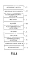
- a method of manufacturing a magneto-resistive device is a method of manufacturing a magneto-resistive device having an MgO layer between a first ferromagnetic layer and a second ferromagnetic layer including a step of forming the first ferromagnetic layer, a step of forming the MgO layer, and a step of forming the second ferromagnetic layer in this order, wherein the step of forming the MgO layer is carried out in a film forming chamber including a component adhered to surface thereof having a substance whose getter effect with respect to oxidizing gas is larger than that of MgO.
- the method of manufacturing a magneto-resistive device is characterized in that the film forming chamber for forming the MgO layer includes at least one film forming means for a substance whose getter effect with respect to the oxidizing gas is larger than MgO, and adhesion of the substance whose getter effect with respect to the oxidizing gas is larger than MgO to the component is carried out by one or a plurality of the film forming means.
- the method of manufacturing a magneto-resistive device according to an example not forming part of the invention is characterized in that the substance whose getter effect with respect to the oxidizing gas is larger than MgO includes at least one element which is included in the substance which constitutes the magneto-resistive device.
- the method of manufacturing a magneto-resistive device is a method of manufacturing a magneto-resistive device having an MgO layer between a first ferromagnetic layer and a second ferromagnetic layer including a step of forming the first ferromagnetic layer, a step of forming the MgO layer, and a step of forming the second ferromagnetic layer in this order, characterized in that the step of forming the MgO layer is carried out in a film forming chamber including a component having a substance whose getter effect with respect to the oxidizing gas is larger than the substance which constitutes the first ferromagnetic layer.
- the method of manufacturing a magneto-resistive device is characterized in that the film forming chamber for forming the MgO layer includes at least one film forming means for a substance whose getter effect with respect to the oxidizing gas is larger than the substance which constitutes the first ferromagnetic layer, and adhesion of the substance whose getter effect with respect to the oxidizing gas is larger than the substance which constitutes the first ferromagnetic layer to the component is carried out by the film forming means.
- the method of manufacturing a magneto-resistive device according to an example not forming part of the invention is characterized in that the substance whose getter effect with respect to the oxidizing gas is larger than the substance which constitutes the first ferromagnetic layer includes at least one element which is included in the substance which constitutes the magneto-resistive device.
- a method of manufacturing a magneto-resistive device is a method of manufacturing a magneto-resistive device having an MgO layer between a first ferromagnetic layer and a second ferromagnetic layer including a step of forming the first ferromagnetic layer, a step of forming the MgO layer, and a step of forming the second ferromagnetic layer in this order, characterized in that the step of forming the MgO layer is carried out in a film forming chamber including a component having a substance whose getter effect with respect to oxidizing gas is maximum from among the substances which constitute the magneto-resistive device adhered to the surface thereof.
- a method of manufacturing a magneto-resistive device is a method of manufacturing a magneto-resistive device having an MgO layer between a first ferromagnetic layer and a second ferromagnetic layer including a step of forming the first ferromagnetic layer, a step of forming the MgO layer, and a step of forming the second ferromagnetic layer in this order, characterized in that the step of forming the MgO layer is carried out in a film forming chamber including a component having a substance whose value of oxygen gas adsorption energy is 145 kcal/mol or higher adhered to the surface thereof.
- a method of manufacturing a magneto-resistive device is a method of manufacturing a magneto-resistive device having an MgO layer between a first ferromagnetic layer and a second ferromagnetic layer including a step of forming the first ferromagnetic layer, a step of forming the MgO layer, and a step of forming the second ferromagnetic layer in this order, characterized in that the step of forming the MgO layer is carried out in a film forming chamber having a component including metal or a semiconductor including at least one of Ta (tantalum), Ti (titanium), Mg (magnesium), Zr (zirconium), Nb (niobium), Mo (molybdenum), W (tungsten), Cr (chrome), Mn (manganese), Hf (hafnium), V (vanadium), B (boron), Si (silicon), Al (aluminum) and Ge (germanium) adhere
- the method of manufacturing a magneto-resistive device according to an example not forming part of the invention is characterized in that the step of forming the MgO layer forms the MgO layer by a sputtering method.
- a method of manufacturing a magneto-resistive device is a method of manufacturing a magneto-resistive device using an apparatus having a plurality of film forming chambers including a first film forming chamber connected to a carrier chamber via a valve being capable of transferring substrates through the plurality of film forming chambers without impairing vacuum, including a first step for adhering a substance whose getter effect with respect to the oxidizing gas is larger than MgO to the surface of a component in the first film forming chamber, a third step carried out after the first step for forming an MgO layer on the substrate in the first film forming chamber, and a second step for carrying out from a next step of the first step to a step before the third step in the film forming chamber other than the first film forming chamber, characterized in that the first step, the second step and the third step are carried out continuously in this order.
- a method of manufacturing a magneto-resistive device is a method of manufacturing a magneto-resistive device using an apparatus having a plurality of film forming chambers including a first film forming chamber connected to a carrier chamber via a valve being capable of transferring substrates through the plurality of film forming chambers without impairing vacuum, including a first step of adhering a substance whose value of oxygen gas adsorption energy is 145 kcal/mol or higher to the surfaces of components in the first film forming chamber, a third step carried out after the first step for forming an MgO layer on the substrate in the first film forming chamber, and a second step for carrying out from a next step of the first step to a step before the third step in the film chamber other than the first film forming chamber, characterized in that the first step, the second step and the third step are carried out continuously in this order.
- a method of manufacturing a magneto-resistive device is a method of manufacturing a magneto-resistive device using an apparatus having a plurality of film forming chambers including a first film forming chamber connected to a carrier chamber via a valve being capable of transferring substrates through the plurality of film forming chambers without impairing vacuum, including a first step for adhering metal or a semiconductor including at least one of Ta, Ti, Mg, Zr, Nb, Mo, W, Cr, Mn, Hf, V, B, Si, Al and Ge to the surface of a component in the first film forming chamber, a third step carried out after the first step for forming an MgO layer on the substrate in the first film forming chamber, and a second step for carrying out from a next step of the first step to a step before the third step in the film forming chamber other than the first film forming chamber, characterized in that the first step, the second step and the third step are carried out continuously in this order
- the method of manufacturing a magneto-resistive device according to an example not forming part of the invention is characterized in that the first step adheres the substance whose getter effect with respect to the oxidizing gas is large to the surface of the component in the first film forming chamber and, simultaneously, forms a film on the substrate.
- the method of manufacturing a magneto-resistive device according to an example not forming part of the invention is characterized in that the first step is carried out in parallel with the step of forming a film on the substrate in the film forming chamber other than the first film forming chamber.
- the method of manufacturing a magneto-resistive device according to an example not forming part of the invention is characterized in that the third step forms the MgO layer by a sputtering method.
- a method of manufacturing a magneto-resistive device is a method of manufacturing a magneto-resistive device using an apparatus having a plurality of film forming chambers including a first film forming chamber connected to a carrier chamber via a valve being capable of transferring substrates through the plurality of film forming chambers without impairing vacuum, including a step of transferring the substrate to the first film forming chamber, sputtering Mg in the first film forming chamber and forming an Mg layer on the substrate and, simultaneously, adhering Mg to the surfaces of components in the first film forming chamber, and a subsequent step of forming an MgO layer in the first film forming chamber.
- An apparatus for manufacturing a magneto-resistive device is characterized in that a film forming chamber for forming an MgO layer includes means for adhering a substance whose getter effect with respect to oxidizing gas is larger than MgO to the surface of a component in the film forming chamber provided therein.
- An apparatus of manufacturing a magneto-resistive device is an apparatus of manufacturing a magneto-resistive device having an MgO layer between a first ferromagnetic layer and a second ferromagnetic layer including means for adhering a substance whose getter effect with respect to oxidizing gas is larger than the substance which constitutes a first ferromagnetic layer to the surfaces of components in the film forming chamber in the film forming chamber for forming the MgO layer.
- the apparatus of manufacturing a magneto-resistive device according to an example not forming part of the invention is characterized in that the substance whose getter effect with respect to the oxidizing gas is large is a substance having the largest getter effect with respect to the oxidizing gas in the substances which constitute the magneto-resistive device.
- An apparatus of manufacturing a magneto-resistive device includes means for adhering a substance whose value of oxygen gas adsorption energy is 145 kcal/mol or higher to the surfaces of components in the film forming chamber in the film forming chamber for forming an MgO layer.
- An apparatus of manufacturing a magneto-resistive device includes means for adhering metal or a semiconductor including at least one of Ta, Ti, Mg, Zr, Nb, Mo, W, Cr, Mn, Hf, V, B, Si, Al and Ge to the surface of the component in the film forming chamber in the film forming chamber for forming an MgO layer.
- the apparatus of manufacturing a magneto-resistive device has a plurality of film forming chambers including the film forming chamber connected to a carrier chamber for forming the MgO layer via a valve being capable of transferring substrates through the plurality of film forming chambers without impairing vacuum.
- the apparatus of manufacturing a magneto-resistive device is characterized in that a target of MgO is provided in the film forming chamber for forming the MgO layer, and an electric power supply unit for supplying an electric power to the target is provided.
- a method of manufacturing a magneto-resistive device is a method of manufacturing a magneto-resistive device having an MgO layer between a first ferromagnetic layer and a second ferromagnetic layer, including a step of forming the first ferromagnetic layer, a step of forming the MgO layer, and a step of forming the second ferromagnetic layer, characterized in that the step of forming the MgO layer is carried out in a state in which a substrate is at a floating potential.
- a method of manufacturing a magneto-resistive device is a method of manufacturing a magneto-resistive device having a substrate, a first ferromagnetic layer, a second ferromagnetic layer and an MgO layer formed between the first ferromagnetic layer and the second ferromagnetic layer, including a step of forming the first ferromagnetic layer on the substrate, a step of forming the MgO layer, and a step of forming the second ferromagnetic layer, characterized in that the step of forming the MgO layer is carried out by placing the substrate on a substrate stage having a portion which comes into contact with the substrate formed of an insulating substance.
- the method of manufacturing a magneto-resistive device according to an example not forming part of the invention is characterized in that the substrate is placed on the substrate stage on which the insulating substance is sprayed.
- the method of manufacturing a magneto-resistive device according to an example not forming part of the invention is characterized in that the substrate is placed on the substrate stage formed of the insulating substance.
- the method of manufacturing a magneto-resistive device according to an example not forming part of the invention is characterized in that the step of forming the MgO layer is carried out in a state in which a mask is arranged on a peripheral portion of the substrate so as to be apart from the substrate.
- a method of manufacturing a magneto-resistive device is a method of manufacturing a magneto-resistive device having an MgO layer between a first ferromagnetic layer and a second ferromagnetic layer, including a step of forming the first ferromagnetic layer, a step of forming the MgO layer and a step of forming the second ferromagnetic layer, characterized in that the step of forming the MgO layer is carried out in a state in which the substrate and a substrate holding holder for holding the substrate are electrically insulated.
- the method of manufacturing a magneto-resistive device according to an example not forming part of the invention is characterized in that the step of forming the MgO layer is carried out in a state in which a mask electrically insulated from the substrate is arranged in the peripheral portion of the substrate.
- An apparatus for manufacturing a magneto-resistive device is an apparatus of manufacturing a magneto-resistive device having an MgO layer between a first ferromagnetic layer and a second ferromagnetic layer including means for bringing a substrate into a state of being at a floating potential in a film forming chamber for forming the MgO layer.
- An apparatus of manufacturing a magneto-resistive device is an apparatus of manufacturing a magneto-resistive device having an MgO layer between a first ferromagnetic layer and a second ferromagnetic layer including means for electrically insulating a substrate and a substrate holder for holding the substrate in a film forming chamber for forming the MgO layer.
- the MgO layer is formed on the substrate in a state in which the substance whose getter effect with respect to oxygen or water or the like (hereinafter, referred to as oxidizing gas) is large is adhered to the surface of the component in the film forming chamber for forming the MgO layer. Accordingly, even when the thickness of the MgO film is small, the magneto-resistive device with a high MR ratio is obtained and, consequently, the magneto-resistive device at a high MR ratio is obtained with a low value of RA.
- oxidizing gas the substance whose getter effect with respect to oxygen or water or the like
- the oxidizing gas such as oxygen or water discharged from the film forming means during formation of the MgO layer is taken by the substance whose getter effect with respect to the oxidizing gas such as oxygen or water is large and hence is removed, so that the MgO layer is formed in a state in which not much residual gas exists in the film forming chamber.
- the steps may be reduced.
- the step of forming the MgO insulator layer is important from among the thin layers which constitute the magneto-resistive device, and the property of the magneto-resistive device is significantly affected by the type of the substance adhered to the surface of the component in the film forming chamber for forming the MgO insulator layer.
- the magneto-resistive device at a high MR ratio is obtained even with the low value of RA.
- the present invention is achieved on the basis of the knowledge as described above.
- the MgO layer is formed in the state in which the substrate is at the floating potential, or in the state in which the substrate and the substrate holder for holding the substrate are electrically insulated, so that the magneto-resistive device at the high MR ratio is obtained even though the thickness of the MgO film is small and, consequently, the magneto-resistive device at the high MR ratio was obtained even with the low value of RA.
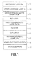
- FIG. 1 is a drawing showing an example of a configuration of a thin film of a magneto-resistive device having an MgO insulator layer, which is manufactured in the first embodiment.
- a lower electrode layer 9 (film thickness: 10 nm) formed of Ta (tantalum), a PtMn (platinum manganese) antiferromagnetic layer 8 (film thickness: 15 nm) formed of PtMn (platinum manganese), a CoFe (cobalt iron) layer 6 (film thickness: 2.5 nm), an Ru (ruthenium) layer 5 (film thickness: 0.85 nm), a first ferromagnetic layer 2 (film thickness: 3 nm) formed of CoFeB (cobalt iron boron), MgO layer 4 (film thickness: 1.0 nm) formed of MgO (magnesium oxide), a second ferromagnetic layer 3 (film thickness: 3 nm) formed of CoFeB, an upper electrode layer 10 (film thickness: 10 nm) formed of Ta, and an Ru layer 11 (film thickness: 7nm
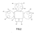
- FIG. 2 is a plane pattern diagram showing an example of a configuration of a film forming chamber in the manufacturing apparatus according to the first embodiment, including a carrier chamber 43, a load lock chamber 44, unload lock chamber 45, a first film forming chamber 21, a second film forming chamber 41 and a third film forming chamber 42 which are each able to exhaust air to a vacuum state.
- the load lock chamber 44 and the unload lock chamber 45 are connected to the carrier chamber 43 via valves, whereby substrates may be transferred between an outer space at an atmospheric pressure and the interior of the vacuum apparatus.
- the first film forming chamber 21, the second film forming chamber 41 and the third film forming chamber 42 are connected to the carrier chamber 43 via the valves. Accordingly, mutual transfer among the respective film forming chambers is achieved while maintaining the vacuum state.
- Each film forming chamber includes film forming means for forming the respective layers described above of the magneto-resistive device.
- the first film forming chamber 21 is provided with first Ta film forming means 46 and MgO film forming means 47
- the second film forming chamber 41 is provided with PtMn film forming means 48
- the third film forming chamber 42 is provided with an Ru film forming means 51 and CoFeB film forming means 52.
- the substrates are transferred through the respective film forming chambers without being exposed to an atmosphere, and are each formed with films in sequence by the film forming means which forms the respective layers of the magneto-resistive device.
- Fig. 3 is a cross-sectional view for explaining an internal configuration of the first film forming chamber in the manufacturing apparatus shown in Fig. 2 .
- the internal configurations of the second film forming chamber and the third film forming chamber are the same as the first film forming chamber other than that films of different substances are formed respectively.
- the film forming means in this embodiment employs a sputtering method.
- the first film forming chamber 21 is connected to a carrier chamber via a valve 34, and air-tightness in the interior thereof is maintained by closing the valve 34.
- the first film forming chamber 21 is provided with a substrate holder 29 for holding a substrate 12 on the lower portion thereof.
- the surface of the substrate holder 29 is covered with an insulator formed of aluminum nitride.
- the film forming means each include a target as a film forming substance and a power supply unit for the target as principal elements.
- a target 24 formed of MgO is attached to a target mounting portion 23.
- a target 26 formed of Ta is attached to a target mounting portion 25 by being partitioned by a partitioning plate 22.
- the target 24 (MgO) and the target 26 (Ta) receive a supply of high-frequency power from a high-frequency power source (not shown in the drawing) via the target mounting portions 23, 25.
- a shutter 27 for shielding the target 24 (MgO) and a shutter 28 for shielding the target 26 (Ta) are provided, and the substrate 12 is shielded by a shutter 31.
- the shutters 27, 28, 31 are each adapted to be retracted individually from positions shown in the drawing according to the sputtering of the target 24 (MgO) or the target 26 (Ta).
- the first film forming chamber 21 is provided with a cylindrical adhesion preventing shield 36 so as to cover the side surface of a film forming chamber inner wall 37.
- the film forming chamber inner wall, the adhesion preventing shield, the shutters, the partitioning plate or the like are referred to as components, hereinafter.
- the first film forming chamber 21 is provided at the lower portion thereof with a vacuum exhausting means 35 for exhausting air from the film forming chamber 21 and bringing the interior thereof into a vacuum state.
- Fig. 2 a method of carrying out the film forming process to form the magneto-resistive device as an example shown in Fig. 1 according to the first embodiment of the invention will be described.
- the Si (silicon) substrate 12 formed with SiO 2 (silicone dioxide) is carried into the first film forming chamber 21 for forming the film of the lower electrode layer 9 formed of Ta, and is held by the holder 29.
- the surface of the holder 29 is covered with an insulating substance formed of aluminum nitride, and the substrate 12 is held in an electrically floating state.
- Air is exhausted from the first film forming chamber 21 to a pressure lower than a background pressure 10 -7 Pa before the film formation, Ar (argon) is introduced into the first film forming chamber 21, the pressure therein is adjusted to a predetermined pressure, the shutter 27, the shutter 28 and the shutter 31 are brought into a closed state, a high-frequency power is applied to the Ta target 26, and a pre-sputtering process of Ta is carried out. Subsequently, the shutter 31 and the shutter 28 are brought into an opened state, and a high-frequency power is applied to the Ta target 26 to form a Ta film on the substrate 12.
- Ar argon
- the film forming chamber inner wall 37, the inner walls of the adhesion preventing shield 36, the partitioning plate 22 or the shutters or the like as the components in the interior of the first film forming chamber 21 are partly covered with Ta sputtered from the Ta target 26.
- the areas in which sputter particles are adhered from the Ta target are different depending on the position or the shape of the target, the position or the shape of the components in the film forming chamber, and the film forming conditions.
- the shutter 31 is brought into a closed state, and the high-frequency power to be applied to the Ta target 26 is turned off.
- the substrate 12 formed with the Ta lower electrode layer 9 is carried out from the first film forming chamber 21, and is transferred to the second film forming chamber 41 provided with the PtMn film forming means 48 and the CoFe film forming means 49, and held by the holder.
- the PtMn layer 8 is formed on the substrate using the PtMn film forming means 48, and then the CoFe layer 6 is formed using the CoFe film forming means 49.
- the substrate 12 is carried out from the second film forming chamber 41, is transferred to the third film forming chamber 42 provided with the Ru film forming means 51 and the CoFeB film forming means 52, and held by the holder.
- the Ru layer 5 is formed on the substrate using the Ru film forming means 51, and then the CoFeB ferromagnetic layer 2 formed of CoFeB is formed using the CoFeB film forming means 52. In this manner, the PtMn antiferromagnetic layer 8, the CoFe antiferromagnetic layer 6, the Ru layer 5 and the first ferromagnetic layer 2 shown in Fig. 1 are formed in sequence.
- the background pressure in the respective film forming chambers before film formation is 10 -7 Pa or lower.
- the substrate 12 having the layers up to the first ferromagnetic layer 2 laminated thereon in Fig. 1 is carried into the first film forming chamber 21 again for forming next the MgO layer 4 and held by the substrate holder 29. At this time, the surfaces of the components in the first film forming chamber 21 are adhered on top thereof with Ta which has sputtered in the step of forming the Ta layer on the substrate.
- a film of the MgO layer is formed by sputtering on the substrate 12.
- An MgO pre-sputtering process is carried out by bringing the shutter 28, the shutter 27 and the shutter 31 in the closed state and applying a high-frequency power to the MgO target 24. Then, the shutter 27 is brought into an opened state, and MgO is sputtered for a predetermined time period. Then, the shutter 31 is brought into an opened state, and the MgO layer 4 is formed on the substrate 12.
- the substrate 12 is carried out from the first film forming chamber 21, and is moved to the third film forming chamber 42 provided with the CoFeB film forming means 52, where the second ferromagnetic layer 3 formed of CoFeB is formed. Subsequently, the substrate 12 is carried into the first film forming chamber 21 again where the first Ta film forming means 46 is arranged, where the Ta upper electrode layer 10 is formed thereon. Subsequently, the substrate 12 is moved to the third film forming chamber 42 where the Ru film forming means 51 is provided, where the Ru antioxidant layer 11 is formed.
- the magneto-resistive device shown in Fig. 1 thus formed demonstrates a preferable performance having a high MR ratio even though the thickness of the film layer of the MgO is small. Consequently, the magneto-resistive device with a high MR ratio is obtained even with a low value of RA.
- the film forming means for the substance whose getter effect with respect to the oxidizing gas is the largest (Ta in this embodiment) from among the substances which constitute the magneto-resistive device is provided in the first film forming chamber provided with the film forming means for MgO, so that only the film of the substance whose getter effect with respect to the oxidizing gas is the largest (Ta in this embodiment) from among the substances which constitute the magneto-resistive device and the MgO film are formed in the first film forming chamber for forming the MgO film.
- the getter effect of Ta to be adhered to the surface of the components in the film forming chamber for forming the MgO layer with respect to the oxidizing gas is higher than the getter effect of MgO or CoFeB for forming the first ferromagnetic layer with respect to the oxidizing gas.
- Fig. 4 is a drawing showing a result of comparison of the film thickness/MR ratio characteristics of the MgO layer of the magneto-resistive device between the manufacturing method according to the present invention and the manufacturing method in the related art
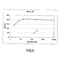
- Fig. 5 is a drawing of comparison of the RA/MR ratio characteristic of the MgO layer of the magneto-resistive device between the manufacturing method according to the present invention and the manufacturing method in the related art.
- the Ta lower electrode layer and the Ta upper electrode layer are formed using the second Ta film forming means 50 provided in the second film forming chamber 41.
- the MgO layer is formed in the film forming chamber in which MgO is adhered to the surfaces of the components in the first film forming chamber for forming the MgO layer.
- the MgO film thickness/MR ratio characteristic of the magneto-resistive device manufactured in the manufacturing method in the present invention in which the MgO layer is formed in the film forming chamber to which Ta is adhered is represented by hollow squares ( ⁇ ) and the MgO film thickness/MR ratio characteristic of the magneto-resistive device manufactured in the manufacturing method in the related art in which the MgO layer is formed without adhesion of Ta is represented by solid diamonds ( ⁇ ).
- the magneto-resistive device with a high MR ratio was obtained even when the film thickness of the MgO layer was reduced to 0.9 nm according to the manufacturing method in the present invention.
- the RA/MR ratio characteristic of the magneto-resistive device manufactured in the manufacturing method in the present invention is represented by hollow squares ( ⁇ ) and the RA/MR ratio characteristic of the magneto-resistive device manufactured in the manufacturing method in the related art is represented by solid diamonds ( ⁇ ). While the MR ratio when the RA is about 150 ⁇ m 2 does not reach 50% in the manufacturing method in the related art, the MR ratio when the RA is about 2 ⁇ m 2 reaches about 130% according to the manufacturing method in the present invention, so that the magneto-resistive device with a high MR ratio was obtained with a low value of RA.
- the surfaces of the components in the film forming chamber when forming the film of MgO were covered with Ta which provides a larger getter effect with respect to the oxidizing gas discharged when forming the MgO film so as to have a high getter effect with respect to the oxidizing gas discharged when forming the MgO film, oxidation of the surface of the ferromagnetic layer 2 and deterioration of the formed film quality of the MgO layer 4 were prevented.
- the respective thin film layers of the magneto-resistive device were formed in the film forming chamber which was exhausted into a vacuum state with a background pressure of 10 -7 or lower Pa.
- adhering Ta which is a substance whose getter effect with respect to the oxidizing gas is large to the surfaces of the components in the MgO film forming chamber, lowering of the MR ratio when the thickness of the MgO film is small was not improved even when the magneto-resistive device was formed by setting the background pressure to 10 -7 Pa and forming the MgO insulator layer.
- MgO is a substance of sodium monoxide which easily adsorb water, and the sintered compact of MgO is porous substance, so that it is considered that the oxidizing gas such as oxygen or water is adsorbed to the MgO target. Even when the background pressure is adjusted to 10 -7 Pa by exhausting air, the oxidizing gas adsorbed to the target cannot be exhausted easily, and the oxidizing gas is discharged into a film forming space during MgO film formation from the MgO target which is shocked by ion simultaneously with the start of sputtering of MgO.
- the substance whose getter effect with respect to the oxidizing gas such as oxygen or water is large is not limited to Ta, and Ti, Mg, Zr, Nb, Mo, W, Cr, Mn, Hf, V, B, Si, Al and Ge may also be applicable.
- An alloy formed of two or more substances whose getter effects with respect to the oxidizing gas are large is also be possible.
- Ta on the Ta lower electrode layer 9 and on the upper electrode layer 10 which constitute the magneto-resistive device is formed in the first film forming chamber 21 for forming a film of MgO in the first embodiment, Ta may be adhered relatively thickly and over a wide range to the MgO film forming chamber, so that a large getter effect is achieved.
- the first embodiment it is also possible to insert a step of adhering Ta to the surface of the components in the first film forming chamber 21 just before forming the MgO layer 4.
- Ta is adhered in addition to Ta which is adhered to the surface of the components in the first film forming chamber 21 in the step of forming the Ta layer which constitutes the magneto-resistive device, so that the thickness of Ta to be adhered to the surface of the components in the first film forming chamber 21 and the area to adhere Ta may be increased.
- the Ta since the Ta may be adhered to the interior of the film forming chamber just before the step of forming the MgO layer, it is considered that a high getter effect is achived with respect to the oxidizing gas discharged when forming the MgO film.
- the substrate 12 is out of the first film forming chamber 21 (for example, during the film forming process of the first ferromagnetic layer 2)
- the thickness of Ta to be adhered to the surfaces of the components in the first film forming chamber 21 may be increased, and the area to be adhered may be increased. Therefore, the getter effect with respect to the oxidizing gas to be discharged when forming the MgO film may be increased.
- the sputtering step for adhering Ta to the surfaces of the components in the first film forming chamber 21 may be carried out by placing a dummy substrate on the substrate holder instead of operation to bring the shutter 31 into the closed state.
- Fig. 6 is a drawing showing an example of a configuration of a thin film of the magneto-resistive device having the MgO insulator layer according to the second embodiment of the present invention.
- a lower electrode portion 64 is formed in Fig. 6 .
- the lower electrode portion 64 includes a first Ta layer 61a, a CuN layer 62, and a second Ta layer 61b.
- the thin film structures of other portions of the magneto-resistive device are the same as those in Fig. 1 according to the first embodiment.
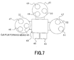
- Fig. 7 is a schematic diagram of a manufacturing apparatus used in the second embodiment of the present invention.
- a CuN film forming means 65 is newly provided in the first film forming chamber in the manufacturing apparatus in Fig. 2 which is used in the first embodiment.
- film forming means of a substance whose getter effect with respect to the oxidizing gas is large (Ta) and film forming means of a substance whose getter effect with respect to the oxidizing gas is small (CuN) are both provided in the first film forming chamber having the film forming means for forming the film of MgO.
- FIG. 6 and Fig. 7 an example of the magneto-resistive device regarding a method of film forming process according to the second embodiment of the manufacturing apparatus and the manufacturing method of the present invention.
- the film formation is carried out in the first film forming chamber 21 in which the first Ta film forming means 46 is provided in order to form the film of the first Ta layer 61a of the lower electrode portion 64 (see Fig. 6 ).
- Ta is adhered to part of the surfaces of the film forming chamber inner wall 37, the adhesion preventing shield 36, the partitioning plate 22 and the shutters or the like, which are the components in the first film forming chamber 21.
- the CuN layer 62 provided in the first film forming chamber 21 the CuN layer 62 of the lower electrode portion 64 is formed (see Fig. 6 ).
- sputtered CuN is adhered to the interior of the first film forming chamber 21.
- a film of Ta is formed on the substrate 12 in order to form the second Ta layer 61b of the lower electrode portion 64 (see Fig. 6 ).
- Ta as the substance whose getter effect with respect to the oxidizing gas is large is adhered to the outermost surface of the components in the first film forming chamber 21.
- the substrate 12 formed with the Ta lower electrode portion 64 is carried out from the first film forming chamber 21, is moved through the second film forming chamber 41 provided with the respective film forming means for PtMn and CoFe, the third film forming chamber 42 provided with the respective film forming means of Ru and CoFeB in sequence, and the PtMn antiferromagnetic layer 8, the CoFe layer 6, the Ru layer 5 and the first ferromagnetic layer 2 formed of CoFeB are formed in sequence as in the first embodiment.
- the background pressures in the respective film forming chambers before film formation is 10 -7 Pa or lower.
- the substrate 12 is carried into the first film forming chamber 21, and the MgO film is sputtered by the MgO film forming means 47.
- the interior of the first film forming chamber 21 is in a state in which Ta whose getter effect with respect to the oxidizing gas is large is adhered to the surface thereof.
- the substrate 12 formed with layers up to the MgO layer 4 moves to the third film forming chamber 42 in which the CoFeB film forming means is provided, where the second ferromagnetic layer 3 formed of CoFeB is formed thereon.
- the substrate 12 is carried again to the first film forming chamber 21, where the film of Ta is formed on the substrate by the first Ta film forming means.
- the substrate is moved to the third film forming chamber 42, and the Ru layer 11 is formed by the Ru film forming means 51, and the magneto-resistive device having the thin film structure shown in Fig. 6 is formed.
- both the film forming means for the substance whose getter effect with respect to the oxidizing gas is the largest (Ta in this embodiment) from among the substances which form the thin film layer which constitute the magneto-resistive device in this embodiment and the film forming means for the substance whose getter effect with respect to the oxidizing gas is small (CuN in this embodiment) from among the same are provided in the first film forming chamber for forming the film of MgO.
- the substance whose getter effect with respect to the oxidizing gas is small to the surface of the components in the first film forming chamber, the substance whose getter effect with respect to the oxidizing gas is large is adhered thereto, and then the MgO film is formed in a state in which the substance whose getter effect with respect to the oxidizing gas is large is adhered to the interior of the first film forming chamber.
- the magneto-resistive device shown in Fig. 6 formed in this manner demonstrated a preferable performance having a high MR ratio even though the thickness of the film of the MgO layer was small. Consequently, the magneto-resistive device with a high MR ratio was obtained even with a low value of RA.
- the substrate since the first Ta layer, the CuN layer and the second Ta layer could be formed continuously in the one film forming chamber, the substrate could be carried simply, and the process time may be reduced.
- the second embodiment of the present invention includes the film forming means for the substance whose getter effect with respect to the oxidizing gas is small and means for adhering the substance whose getter effect with respect to the oxidizing gas is large to the surfaces of the components in the first film forming chamber for forming the MgO layer, and includes a step of adhering the substance whose getter effect with respect to the oxidizing gas is large (Ta in this embodiment) to the surface of the components in the film forming chamber before forming the film of MgO so that the substance whose getter effect with respect to the oxidizing gas is large is adhered to the surface of the components in the film forming chamber after the substance whose getter effect with respect to the oxidizing gas is small is adhered right before forming the MgO layer.
- the film forming means for the MgO film, the film forming means for Ta and the film forming means for CuN are provided in the film forming chamber for forming the MgO layer.
- Ta has the highest getter effect with respect to the oxidizing gas from among the substances to be adhered by the film forming means.
- the getter effect of Ta to be adhered to the surfaces of the components in the film forming chamber for forming the MgO layer with respect to the oxidizing gas is larger than the getter effect of the CoFeB which constitutes MgO or the first ferromagnetic layer with respect to the oxidizing gas.
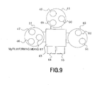
- Fig. 8 is a drawing showing an example of the thin film configuration of the magneto-resistive device having the MgO insulator layer in the first example not forming part of the present invention. As shown in Fig. 8 , in the first example, an Mg layer 66 is provided under the MgO layer 4 in the thin film configuration of the magneto-resistive device in Fig. 1 .
- Fig. 9 is a schematic diagram of the apparatus of manufacturing used in the first example.
- the manufacturing apparatus used in the first example in Fig. 9 is provided newly with an Mg film forming means 67 in the first film forming chamber in the manufacturing apparatus used in the first embodiment.
- the Si substrate 12 formed with SiO 2 on the surface thereof is carried into the first film forming chamber 21 to form the lower electrode layer 9 of Ta on the substrate 12.
- Ta sputtered from the Ta target 26 is adhered on part of the film forming chamber inner wall 37, the adhesion preventing shield 36, the partitioning plate 22 or the shutter or the like in the interior of the first film forming chamber 21.
- the substrate 12 is moved through the second film forming chamber 41 provided with the respective film forming means for PtMn and CoFe and the third film forming chamber 42 provided with the respective means for Ru and CoFeB in sequence, and the substrate formed with layers up to the PtMn antiferromagnetic layer 8, the CoFe layer 6, the Ru layer 5 and the first ferromagnetic layer 2 formed of CoFeB shown in Fig. 9 are formed in sequence.
- the respective thin film layers are formed by exhausting the air from the respective film forming chambers to achieve a background pressure of 10 -7 Pa or lower.
- the substrate 12 formed with the layers up to the ferromagnetic layer 2 in sequence is carried again into the first film forming chamber 21 to sputter the Mg target of the Mg film forming means 67 and form the Mg layer 66.
- Mg sputtered from the Mg target is adhered on part of the film forming chamber inner wall 37, the adhesion preventing shield 36, the partitioning plate 22 or the shutter in the interior of the first film forming chamber 21.
- Mg is a substance whose getter effect with respect to the oxidizing gas is large, and is a substance whose getter effect with respect to oxygen or water or the like is large.
- the MgO target of the MgO film forming means 47 is sputtered to sputter the MgO layer 4 on the substrate 12 in the state of the film forming chamber as described above.
- the substrate 12 formed with layers up to the MgO layer 4 is moved to the third film forming chamber 42, where the second ferromagnetic layer 3 formed of CoFeB is formed thereon. Subsequently, the substrate moves again to the first film forming chamber 21 to form the Ta upper electrode layer 10 thereon. Then, the substrate 12 is moved to the third film forming chamber 42 to form the Ru layer. In this manner, the magneto-resistive device having the thin film configuration shown in Fig. 8 is formed.
- the magneto-resistive device formed in this manner demonstrated a preferable performance having a high MR ratio even though the thickness of the film of the MgO layer is small. Consequently, the magneto-resistive device with a high MR ratio was obtained even with a low value of RA.
- the substance whose getter effect with respect to the oxidizing gas to be adhered to the surfaces of the components in the first film forming chamber for forming the film of MgO is large is Mg.
- MgO layer is formed continuously after the Mg layer, Mg is adhered to the surfaces of the components in the first film forming chamber right before forming the film of MgO, and hence it is considered that a high getter effect is obtained from Mg to be adhered to the surfaces of the components in the first film forming chamber for forming the film of MgO in this example.
- the extent of the getter effect with respect to the oxidizing gas varies depending on the state of the surface of the substance. Since the Mg film is adhered to the surfaces of the components in the film forming chamber right before forming the MgO layer, the surface of the adhered Mg film is in a clean state, so that it is considered that a higher getter effect is achieved.
- the Mg layer is formed in the film forming chamber for forming the MgO layer and, in addition, the Ta layer is formed
- Mg and Ta which are substances whose getter effects with respect to the oxidizing gas are large, are adhered to the surfaces of the components in the MgO film forming chamber, the substances whose getter effect with respect to the oxidizing gas is large may be formed further thickly and over a larger area, so that the higher effect is achieved.
- the Ta electrode layer must be formed in the MgO film forming chamber, and the same effect is achieved even when only the Mg layer is formed in the MgO film forming chamber and the Ta layer is formed in a film forming chamber different from the film forming chamber for forming the MgO layer.
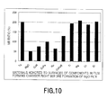
- a drawing is presented showing a result of comparison of measured MR ratios of the magneto-resistive devices obtained by forming the MgO film on the substrates 12 having the configuration shown in Fig. 1 in a state in which various substances are adhered to the surfaces of the components in the first film forming chamber for forming the MgO layer right before forming the MgO layer on the substrates 12.
- the method of execution will be described according to an example in which Ti is employed as the substance to be adhered to the surfaces of the components in the first film forming chamber for forming the film of MgO.
- the Ti film forming means is provided in the first film forming chamber in addition to the MgO film forming means, the Ta film forming means.
- the layers up to the first ferromagnetic layer 2 are laminated in sequence on the substrate 12. Ta is adhered to the surfaces of the components in the first film forming chamber when the Ta lower electrode layer is formed.
- a step of adhering Ti in the first film forming chamber 21 is inserted right before forming the MgO layer 4.
- the magneto-resistive device is formed by carrying the substrate 12 having laminated with layers up to the first ferromagnetic layer 2 in sequence to the first film forming chamber 21, holding the same by the substrate holder 29, opening the target shutter of Ti in a state in which the shutter 31 is closed and hence the substrate 12 is shielded, and sputtering Ti to adhere Ti to the surfaces of the film forming chamber inner wall 37, the adhesion preventing shield 36, the shutter and the partitioning plate 22.
- the MgO layer 4 is formed on the substrate 12 in the same manner as the first embodiment.
- the thin film is laminated in the same manner as in the first embodiment, so that the magneto-resistive device is formed.
- the magneto-resistive device is formed by forming the MgO layer in a state in which various substances are adhered to the surfaces of the components in the film forming chamber, and the MR ratios were measured. Consequently, while the MR ratio was about 50% when the MgO layer is sputtered by adhering MgO, the values of MR ratio of about 70 to 130% were obtained when the MgO layer is sputtered by adhering CuN, CoFe, Ru and CoFeB. It was found that the values of the MR ratio obtained when sputtering the MgO layer by adhering Ta, Ti, Mg, Cr and Zr were as high as about 190% to 2100.
- the substance to adhere to the surfaces of the components in the film forming chamber for forming the film of MgO is a substance whose getter effect is larger than MgO, the effect to improve the element characteristic is achieved.
- Ti, Cr, Zr or the like other than Ta in the first and second embodiments and Mg in the first example not forming part of the present invention are selected as needed as a substance to be adhered to the surfaces of the components in the film forming chamber for forming the film of MgO, good effect to improve the element characteristic is achieved.
- the extent of getter effect with respect to the oxidizing gas may be compared with an index of the value of the oxygen gas adsorption energy of the substance in question.
- the values of the oxygen gas adsorption energy of Ti, Ta, Mg, Cr and Zr having a high MR ratio are larger than 145 kcal/mol.
- the substance whose value of oxygen gas adsorption energy is larger than 145 kcal/mol, that is, whose getter effect with respect to the oxidizing gas is large is adhered to the surfaces of the components in the MgO film forming chambers, so that the oxygen gas discharged when forming the film of MgO is sufficiently gettered on the surfaces of the components to the MgO film forming chamber. Accordingly, the magneto-resistive device being subjected to less oxidation of the surface of the ferromagnetic layer or deterioration of the film quality of the formed MgO insulator layer was formed.
- the magneto-resistive device with a high MR ratio is obtained even with a low RA by gettering the oxidizing gas such as oxygen or water discharged during the film forming process of the MgO layer sufficiently as long as it is a substance whose getter effect with respect to the oxidizing gas is large.
- the effect seems to be achieved even with Nb, Mo, W, Mn, Hf, V, B, Si, Al and Ge whose values of oxygen gas adsorption energy is larger than 145 kcal/mol.
- the substance adhered to the film forming chamber inner wall for forming the film of MgO must simply includes a substance whose getter effect with respect to the oxidizing gas is large as a main component.
- the substance to be adhered to the surfaces of the components in the MgO film forming chamber may be formed by selecting a substance whose getter effect with respect to the oxidizing gas is large as needed, and providing the film forming means for the corresponding substance in the MgO film forming chamber.
- a substance whose value of the oxygen gas adsorption energy is 145 kcal/mol or higher is selected as the substance to be adhered to the surfaces of the components in the MgO film forming chamber, so that the oxidizing gas such as oxygen or water to be discharged at the time of forming the film of MgO is sufficiently gettered on the surfaces of the components in the MgO film forming chamber.
- the timing to be adhered to the interior of the MgO film forming chamber is more preferably right before the formation of the MgO film, because it is considered that the extent of the getter effect with respect to the oxidizing gas varies depending on the state of the surface of the substance, and the higher getter effect is obtained when the surface is in a clean state.
- the substance to be adhered to the interior of the MgO film forming chamber is specifically Ta, Ti, Mg, Zr, Nb, Mo, W, Cr, Mn, Hf, V, B, Si, Al and Ge.
- the means for adhering to the interior of the MgO film forming chamber may be used commonly as the means for forming the thin film layer and the steps therefor may be commonly carried out by one step, so that the apparatus may be downsized, and the shortening of the entire process is achieved.
- Fig. 11 is a drawing showing an example of the configuration of a thin film of the magneto-resistive device having the MgO layer which is manufactured in the third embodiment of the present invention
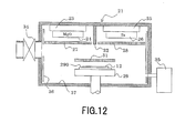
- Fig. 12 is a cross-sectional view for explaining the internal configuration of the first film forming chamber in the manufacturing apparatus in the third embodiment of the present invention
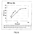
- Fig. 13 is a drawing showing an RA/MR ratio characteristic of the MgO layer of the magneto-resistive device according to the third embodiment of the present invention.
- the components having substantially the same function or the same configuration as those in Fig. 1 , Fig. 3 , Fig. 6 and Fig. 8 are designated by the same reference numerals for description, and detailed description of the identical components is omitted.
- the thin film configuration of the magneto-resistive device having the MgO layer to be manufactured in this embodiment includes a lower electrode portion 640 including the first Ta layer 61a (film thickness: 5.0 nm), a first CuN layer 62a (film thickness: 20 nm), a second Ta layer 61b (film thickness: 3.0 nm) and the second CuN layer 62b (film thickness: 20 nm), a ground layer including a Ta layer 68 (film thickness: 3.0 nm) and an Ru layer 69 (film thickness: 5.0 nm), an antiferromagnetic layer 80 (film thickness: 7.0 nm) formed of IrMn (iridium manganese), the CoFe antiferromagnetic layer 6 (film thickness: 2.5 nm), the Ru layer 5 (film thickness: 0.85 nm), the first ferromagnetic layer 2 (film thickness: 3.0 nm) formed of CoFeB, the insulator layer 4 (film thickness:
- the apparatus for manufacturing the magneto-resistive device having the MgO layer according to this embodiment has substantially the same configuration as the film forming apparatus shown in Fig. 2 and Fig. 7 .
- the first film forming chamber 21 is configured as shown in Fig. 12 .
- the description is given about the configuration in which the surface of the substrate holder 29 is covered with the insulator formed of aluminum nitride (AlN).
- the manufacturing apparatus in this embodiment is characterized in that a substrate stage 290 is provided between the substrate holder 29 and the substrate 12, and the substrate 12 is directly placed on the substrate stage 290.
- the substrate stage 290 must simply have a configuration which is able to insulate at a portion where the substrate holder 29 and the substrate 12 come into contact with each other and, for example, it is also applicable to configure the substrate stage 290 by spraying the insulating substance such as Al 2 O 3 (alumina) on the surface of the stainless steel plate or to configure the substrate stage 290 by itself with the insulating substance. In this manner, the substrate 12 is brought into a state of electrically floated completely (floating state), that is, the substrate 12 is brought to have a floating potential. What is essential is that the substrate 12 is electrically insulated from the substrate stage 290 and the substrate holder 29. The surface of the substrate holder 29 by itself according to this embodiment does not have to be covered with the insulator.
- the insulating substance such as Al 2 O 3 (alumina)
- bringing the substrate 12 to have the floating potential is achieved by means such as insulating the substrate stage 290 from the substrate holder 29, or insulating the substrate holder 29 from the ground in addition to insulating the substrate 12 from the substrate stage 290 as described above.
- the substrate 12 is insulated from the ground at any portion between the substrate 12 and the ground.
- insulating such as interposing an insulating substance, configuring the components such as the substrate stage 290 or the substrate holder 29 by itself with the insulating substance, configuring only the portion to be insulated (portion to come into contact) with an insulating substance, or keeping the portions to be insulated from each other apart from each other.
- the method of manufacturing the magneto-resistive device having the MgO layer in this embodiment is characterized in that the substrate holder 29 is insulated from the substrate 12, and the MgO layer 4 is formed in the state in which the substrate 12 is electrically floated completely (floating state) as described above.
- the step of forming the MgO layer 4 on the substrate 12 in the state in which the substance whose getter effect with respect to the oxidizing gas is large (Ta or the like) is adhered to the surface of the components in the interior of the first film forming chamber 21 for forming MgO layer 4 and other film forming steps are the same as that in the embodiment which is already described, so that detailed description is omitted.
- the substrate 12 When spraying Al 2 O 3 on the surface of the stainless steel panel to configure the substrate stage 290, the substrate 12 is brought into the floating state by spraying the Al 2 O 3 to a thickness of about 0.2 mm.
- the substrate 12 is also brought into the floating state by configuring the substrate stage 290 by itself by an AlN panel (thickness of about 14 mm) as the insulating substance. Therefore, the magneto-resistive device having the MgO layer is manufactured in such the configuration, and the RA/MR ratio characteristics of the MgO layer of the magneto-resistive device are compared ( Fig. 13 ). In Fig.
- (I) represents the characteristic when the substrate stage 290 formed of the stainless steel panel is used
- (II) represents the characteristic when the substrate stage 290 on which Al 2 O 3 is sprayed by a thickness of about 0.2 mm on the surface of the stainless steel panel is used
- (III) represents the characteristic when the substrate stage 290 formed of an AlN panel of a thickness of about 14 mm is used.
- the reason when AlN is selected in the case of (III) is because its coefficient of thermal conductivity is high.
- the film by placing the substrate 12 on the substrate holder 29 via the insulating substance (the substrate stage 290) as in the first embodiment, the extent of lowering of the MR ratio is small even in the low RA area, so that a higher MR ratio is obtained in comparison with the case in the related art, so that achievement of both the low RA and the high MR ratio, which is considered to be difficult in the related art, may be realized.
- the thin film configuration ( Fig. 11 ) of the magneto-resistive device manufactured according to the present embodiment is different from the thin film configuration ( Fig. 1 , Fig. 6 , Fig.
- the same results as described above may be obtained by bringing the substrate 12 into the floating state in the apparatus or the method of manufacturing the magneto-resistive device having the thin film configuration shown in the respective embodiments as well.
- FIG. 14 is a cross-sectional view for explaining the internal structure of the first film forming chamber of the manufacturing apparatus in the sixth embodiment of the present invention.
- the components having substantially the same function or the same configuration as those in Fig. 3 and Fig. 12 are designated by the same reference numerals for description, and detailed description of the identical components is omitted.
- the film forming apparatus or the film forming method for forming the MgO layer 4 on the substrate 12 in a state in which the substance whose getter effect with respect to the oxidizing gas is large (Ta or the like) is adhered to the surfaces of the components in the interior of the first film forming chamber 21 for forming the MgO layer 4 has been described.
- the MgO layer 4 is formed in a state in which the substrate holder 29 is insulated from the substrate 12 and the substrate 12 is electrically floating completely (the state at the floating potential) without adhering the above-described substance (Ta or the like) to the surfaces of the components in the interior of the first film forming chamber 21 for forming the MgO layer 4. Therefore, in the manufacturing apparatus in this example, the same substrate stage 290 which is the same as the substrate stage 290 in the third embodiment described above is provided between the substrate holder 29 and the substrate 12, and the substrate 12 is directly placed on the substrate stage 290.
- the interior of the first film forming chamber 21 must simply be arranged only for MgO as a target as shown in Fig. 14 , and it is not specifically necessary to provide the Ta 26 as a target, the target mounting portion 25, the partitioning plate 22, the shutters 27 and 28 (see Fig. 12 ). Consequently, the extent of lowering of the MR ratio is small even in the low RA area as shown in Fig. 13 , and a larger MR ratio than in the related art is obtained.
- Fig. 15 is a drawing for showing a configuration of the portion near the substrate holder in the manufacturing apparatus in the third example not forming part of the present invention in which (a) is a drawing showing a state in which a mask and the substrate are in contact with each other, (b) is a drawing showing a state in which the mask and the substrate are apart from each other, and Fig. 16 is a drawing showing the RA/MR ratio characteristic of the MgO layer of the magneto-resistive device according to this example.
- the components having substantially the same function and the same configuration as those in Fig. 3 , and Fig. 12 are designated by the same reference numerals for description, and detailed description of the identical components is omitted.
- the metallic mask for covering the peripheral portion of the substrate for holding the same is employed in order to prevent the film from being formed on the back side of the substrate (the side which comes into contact with the substrate holder) by film forming particles running to the backside thereof (see Fig. 15(a) , reference numeral 295).
- this example is adapted to carry out the step of forming the MgO layer 4 in a state of providing the substrate stage 290 described above between the substrate holder 29 and the substrate 12, placing the substrate 12 directly on the substrate stage 290, and keeping a metallic mask 295 apart from the substrate 12 in the state in which the substrate 12 is at the floating potential as shown in Fig.
- the mask 295 and the substrate 12 must simply be kept apart from each other by a distance which is able to prevent sputter particles from running to the backside of the substrate 12, and for example, is set to 0.5 mm. In this manner, by bringing the mask 295 and the substrate 12 apart from each other, the mask 295 and the substrate 12 are brought into the electrically insulated state.
- the mask is a component for covering the peripheral portion of the substrate for preventing the film from being formed by the film forming particles running to the backside of the substrate in a case of carrying out the film forming process on the substrate.
- the magneto-resistive device having the MgO layer is manufactured on the basis of the respective cases where the mask 295 is brought into contact with the peripheral portion of the substrate 12 as shown in Fig. 15(a) , and where the mask 295 and the substrate 12 are brought apart from each other as shown in Fig. 15(b) , and the RA/MR ratio characteristics of the MgO layer of the magneto-resistive device having the MgO layer are compared ( Fig. 16 ).
- solid triangles ( ⁇ ) represent the characteristics when the mask 295 is brought into contact with the peripheral portion of the substrate 12
- solid circles ( ⁇ ) represent a characteristic in the case in which the mask 295 and the substrate 12 are brought apart from each other.
- a higher MR ratio is obtained in the case ( ⁇ ) in which the mask 295 and the substrate 12 are brought apart from each other than the case (solid triangle) in which the mask 295 and the substrate 12 are brought into contact with each other at a point where the RA is 5 ⁇ - ⁇ m 2 , and as a whole, the subject to achieve both low RA and high MR ratio is realized further preferably in the case ( ⁇ ) in which the mask 295 and the substrate 12 are brought apart from each other.
- the mask 295 and the substrate 12 are brought into the electrically insulated state by bringing the metallic mask 295 and the substrate 12 apart from each other, and the electric current is prevented from flowing to the MgO layer during the formation of the MgO film and, consequently, prevention of deterioration of the film quality of the MgO layer and deterioration of the characteristic of the magneto-resistive device are achieved.
- the mask 295 and the substrate 12 are brought into the electrically insulated stat by bringing the mask 295 and the substrate 12 apart from each other.
- the state in which the mask 295 and the substrate 12 are electrically insulated may be achieved even when the substrate 12 and the mask 295 are in contact with each other as shown in Fig. 15(a) , so that the same effects as described above are achieved.
- the film forming apparatus in the embodiments has been described as an apparatus having the three film forming chambers, the invention is not limited thereto.
- the apparatus of the present invention is described as an apparatus having two or three film forming means in the film forming chamber, the invention is not limited thereto.
- the apparatus of the present invention is not limited to the shape of the film forming chamber in the apparatus shown in the embodiments.
- the components in the film forming chamber for adhering the substance whose getter effect with respect to the oxidizing gas such as oxygen or water is large have been described as the film forming chamber inner wall, the adhesion preventing shield, the partitioning panel or the shutter, they are not limited thereto. What is important is adhesion to the surfaces of the components in the interior of the film forming chambers, and it may be other configurations.
- the method of forming the respective layers of the magneto-resistive device has been described as the method on the basis of the sputtering, other film forming methods such as deposition or the like are also applicable, and the film forming method is not specifically limited. However, formation of the MgO layer using a non-sputtering method is excluded, in accordance with the claims.
Landscapes
- Chemical & Material Sciences (AREA)
- Engineering & Computer Science (AREA)
- Physics & Mathematics (AREA)
- Analytical Chemistry (AREA)
- Plasma & Fusion (AREA)
- Mechanical Engineering (AREA)
- Organic Chemistry (AREA)
- Metallurgy (AREA)
- Materials Engineering (AREA)
- Chemical Kinetics & Catalysis (AREA)
- Manufacturing & Machinery (AREA)
- Magnetic Heads (AREA)
- Hall/Mr Elements (AREA)
- Mram Or Spin Memory Techniques (AREA)
- Thin Magnetic Films (AREA)
- Measuring Magnetic Variables (AREA)
Description
- The present invention relates to methods of manufacturing a magneto-resistive device used for an MRAM (magnetic random access memory) or a magnetic head sensor.
- A magneto-resistive device is used for an MRAM (magnetic random access memory) or a magnetic head sensor. The magneto-resistive device having a fundamental structure including a first ferromagnetic layer/an insulator layer/a second ferromagnetic layer is, utilizing the property such that the electric resistance is low when the direction of magnetization of the first ferromagnetic layer and the second ferromagnetic layer extend in parallel and is high when in non-parallel, adapted in such a manner that the direction of magnetization of one of the ferromagnetic layers is fixed and the direction of magnetization of the other one of the ferromagnetic layers is variable according to the external magnetic field to detect the direction of external magnetic field as a change in electric resistance. In order to obtain a high detection sensitiveness, high MR ratio (magnetoresistance ratio), which is an index of variation in electric resistance value between the cases in which the direction of magnetization is parallel and non-parallel is required. The inventor proposed a magneto-resistive device using magnesium oxide (although referred to as MgO hereinafter, it does not mean that stoichiometry is 1:1) which is formed into a film by sputtering as an insulator layer of the magneto-resistive device as a configuration in which a high MR ratio is obtained (for example, see Non-Patent
Document 1 and Patent Document 1). - [Non-Patent Document 1] APPLIED PHYSICS LETTERS 86, 092502 (2005)
- Document
US 2006/0042930 A1 describes that, as part of the fabrication of a magnetic tunnel junction (MTJ), a magnesium oxide (MgO) tunnel barrier is reactively sputter deposited from a Mg target in the presence of reactive oxygen gas (02) in the "high-voltage" state to assure that deposition occurs with the Mg target in its metallic mode, i.e., no or minimal oxidation. Because the metallic mode of the Mg target has a finite lifetime, a set of 02 flow rates and associated sputter deposition times are established, with each flow rate and deposition time assuring that deposition occurs with the Mg target in the metallic mode and resulting in a known tunnel barrier thickness. The commencement of undesirable Mg target oxidation is associated with a decrease in target voltage, so the sputtering can also be terminated by monitoring the target voltage and terminating application of power to the target when the voltage reaches a predetermined value. - Further, the document: TSUNEKAWA K ET AL: "Giant tunneling magnetoresistance effect in low-resistance CoFeB/MgO(001)/CoFeB magnetic tunnel junctions for read-head applications", APPLIED PHYSICS LETTERS, AlP, AMERICAN INSTITUTE OF PHYSICS, MELVILLE, NY, US, vol. 87, no. 7, 8 August 2005 (2005-08-08), pages 72503/1-072503/3, XP012077470, ISSN: 0003-6951, DOI: 10.1063/1.2012525; describes introducing an ultrathin Mg metal layer with a thickness of 4 A between a CoFeB bottom electrode layer and an MgO(001) tunnel barrier layer.
- Finally, document
US 2004/0244684 A1 describes a magnetic multilayer film deposition system having a plurality of treatment chambers for depositing a multilayer film including a plurality of magnetic films on a substrate, a conveyance system for conveying the substrate in a state shielded from the atmosphere, a metal film treatment chamber, a treatment system having treating metal film included in the multilayer film in the treatment chamber, an optical measurement system for optically evaluating the surface state of the metal film, and a control system for controlling the operation of the treatment system based on a measurement signal output from this optical measurement system, wherein when depositing a multilayer film on a substrate in the film deposition system, it is possible to manage the surface state of the metal film during the treatment process of the metal film and possible to treat the metal film precisely. - [Patent Document 1] Patent Application
2004-259280 - In order to achieve a higher density of MRAMs or a higher resolution of magnetic heads, it is required to further reduce the size of the element. When the size of the element is reduced, it is necessary to reduce the electric resistance value per 1 µm2 (hereinafter, referred to as RA) sufficiently when the direction of magnetization is parallel for a desirable operation. The RA of the magneto-resistive device is reduced by reducing the thickness of the MgO film of an insulator layer. However, when the thickness of the MgO film is reduced, the MR ratio is significantly lowered and, consequently, there arises a problem such that both the low RA and the high MR ratio cannot be achieved simultaneously.
- It is an object of the present invention to provide a method of manufacturing a magneto-resistive device which achieves a high MR ratio even when the value of RA is low.
- The invention is defined in
independent claims - A method of manufacturing a magneto-resistive device according to an example not forming part of the invention is a method of manufacturing a magneto-resistive device having an MgO layer between a first ferromagnetic layer and a second ferromagnetic layer including a step of forming the first ferromagnetic layer, a step of forming the MgO layer, and a step of forming the second ferromagnetic layer in this order, wherein the step of forming the MgO layer is carried out in a film forming chamber including a component adhered to surface thereof having a substance whose getter effect with respect to oxidizing gas is larger than that of MgO.
- The method of manufacturing a magneto-resistive device according to an example not forming part of the invention is characterized in that the film forming chamber for forming the MgO layer includes at least one film forming means for a substance whose getter effect with respect to the oxidizing gas is larger than MgO, and adhesion of the substance whose getter effect with respect to the oxidizing gas is larger than MgO to the component is carried out by one or a plurality of the film forming means.
- The method of manufacturing a magneto-resistive device according to an example not forming part of the invention is characterized in that the substance whose getter effect with respect to the oxidizing gas is larger than MgO includes at least one element which is included in the substance which constitutes the magneto-resistive device.
- The method of manufacturing a magneto-resistive device according to an example not forming part of the invention is a method of manufacturing a magneto-resistive device having an MgO layer between a first ferromagnetic layer and a second ferromagnetic layer including a step of forming the first ferromagnetic layer, a step of forming the MgO layer, and a step of forming the second ferromagnetic layer in this order, characterized in that the step of forming the MgO layer is carried out in a film forming chamber including a component having a substance whose getter effect with respect to the oxidizing gas is larger than the substance which constitutes the first ferromagnetic layer.
- The method of manufacturing a magneto-resistive device according to an example not forming part of the invention is characterized in that the film forming chamber for forming the MgO layer includes at least one film forming means for a substance whose getter effect with respect to the oxidizing gas is larger than the substance which constitutes the first ferromagnetic layer, and adhesion of the substance whose getter effect with respect to the oxidizing gas is larger than the substance which constitutes the first ferromagnetic layer to the component is carried out by the film forming means.
- The method of manufacturing a magneto-resistive device according to an example not forming part of the invention is characterized in that the substance whose getter effect with respect to the oxidizing gas is larger than the substance which constitutes the first ferromagnetic layer includes at least one element which is included in the substance which constitutes the magneto-resistive device.
- A method of manufacturing a magneto-resistive device according to an example not forming part of the invention is a method of manufacturing a magneto-resistive device having an MgO layer between a first ferromagnetic layer and a second ferromagnetic layer including a step of forming the first ferromagnetic layer, a step of forming the MgO layer, and a step of forming the second ferromagnetic layer in this order, characterized in that the step of forming the MgO layer is carried out in a film forming chamber including a component having a substance whose getter effect with respect to oxidizing gas is maximum from among the substances which constitute the magneto-resistive device adhered to the surface thereof.
- A method of manufacturing a magneto-resistive device according to an example not forming part of the invention is a method of manufacturing a magneto-resistive device having an MgO layer between a first ferromagnetic layer and a second ferromagnetic layer including a step of forming the first ferromagnetic layer, a step of forming the MgO layer, and a step of forming the second ferromagnetic layer in this order, characterized in that the step of forming the MgO layer is carried out in a film forming chamber including a component having a substance whose value of oxygen gas adsorption energy is 145 kcal/mol or higher adhered to the surface thereof.
- A method of manufacturing a magneto-resistive device according to an example not forming part of the invention is a method of manufacturing a magneto-resistive device having an MgO layer between a first ferromagnetic layer and a second ferromagnetic layer including a step of forming the first ferromagnetic layer, a step of forming the MgO layer, and a step of forming the second ferromagnetic layer in this order, characterized in that the step of forming the MgO layer is carried out in a film forming chamber having a component including metal or a semiconductor including at least one of Ta (tantalum), Ti (titanium), Mg (magnesium), Zr (zirconium), Nb (niobium), Mo (molybdenum), W (tungsten), Cr (chrome), Mn (manganese), Hf (hafnium), V (vanadium), B (boron), Si (silicon), Al (aluminum) and Ge (germanium) adhered to the surface thereof.
- The method of manufacturing a magneto-resistive device according to an example not forming part of the invention is characterized in that the step of forming the MgO layer forms the MgO layer by a sputtering method.
- A method of manufacturing a magneto-resistive device according to an example not forming part of the invention is a method of manufacturing a magneto-resistive device using an apparatus having a plurality of film forming chambers including a first film forming chamber connected to a carrier chamber via a valve being capable of transferring substrates through the plurality of film forming chambers without impairing vacuum, including a first step for adhering a substance whose getter effect with respect to the oxidizing gas is larger than MgO to the surface of a component in the first film forming chamber, a third step carried out after the first step for forming an MgO layer on the substrate in the first film forming chamber, and a second step for carrying out from a next step of the first step to a step before the third step in the film forming chamber other than the first film forming chamber, characterized in that the first step, the second step and the third step are carried out continuously in this order.
- A method of manufacturing a magneto-resistive device according to an example not forming part of the invention is a method of manufacturing a magneto-resistive device using an apparatus having a plurality of film forming chambers including a first film forming chamber connected to a carrier chamber via a valve being capable of transferring substrates through the plurality of film forming chambers without impairing vacuum, including a first step of adhering a substance whose value of oxygen gas adsorption energy is 145 kcal/mol or higher to the surfaces of components in the first film forming chamber, a third step carried out after the first step for forming an MgO layer on the substrate in the first film forming chamber, and a second step for carrying out from a next step of the first step to a step before the third step in the film chamber other than the first film forming chamber, characterized in that the first step, the second step and the third step are carried out continuously in this order.
- A method of manufacturing a magneto-resistive device according to an example not forming part of the invention is a method of manufacturing a magneto-resistive device using an apparatus having a plurality of film forming chambers including a first film forming chamber connected to a carrier chamber via a valve being capable of transferring substrates through the plurality of film forming chambers without impairing vacuum, including a first step for adhering metal or a semiconductor including at least one of Ta, Ti, Mg, Zr, Nb, Mo, W, Cr, Mn, Hf, V, B, Si, Al and Ge to the surface of a component in the first film forming chamber, a third step carried out after the first step for forming an MgO layer on the substrate in the first film forming chamber, and a second step for carrying out from a next step of the first step to a step before the third step in the film forming chamber other than the first film forming chamber, characterized in that the first step, the second step and the third step are carried out continuously in this order.
- The method of manufacturing a magneto-resistive device according to an example not forming part of the invention is characterized in that the first step adheres the substance whose getter effect with respect to the oxidizing gas is large to the surface of the component in the first film forming chamber and, simultaneously, forms a film on the substrate.
- The method of manufacturing a magneto-resistive device according to an example not forming part of the invention is characterized in that the first step is carried out in parallel with the step of forming a film on the substrate in the film forming chamber other than the first film forming chamber.
- The method of manufacturing a magneto-resistive device according to an example not forming part of the invention is characterized in that the third step forms the MgO layer by a sputtering method.
- A method of manufacturing a magneto-resistive device according to an example not forming part of the invention is a method of manufacturing a magneto-resistive device using an apparatus having a plurality of film forming chambers including a first film forming chamber connected to a carrier chamber via a valve being capable of transferring substrates through the plurality of film forming chambers without impairing vacuum, including a step of transferring the substrate to the first film forming chamber, sputtering Mg in the first film forming chamber and forming an Mg layer on the substrate and, simultaneously, adhering Mg to the surfaces of components in the first film forming chamber, and a subsequent step of forming an MgO layer in the first film forming chamber.
- An apparatus for manufacturing a magneto-resistive device according to an example not forming part of the invention is characterized in that a film forming chamber for forming an MgO layer includes means for adhering a substance whose getter effect with respect to oxidizing gas is larger than MgO to the surface of a component in the film forming chamber provided therein.
- An apparatus of manufacturing a magneto-resistive device according to an example not forming part of the invention is an apparatus of manufacturing a magneto-resistive device having an MgO layer between a first ferromagnetic layer and a second ferromagnetic layer including means for adhering a substance whose getter effect with respect to oxidizing gas is larger than the substance which constitutes a first ferromagnetic layer to the surfaces of components in the film forming chamber in the film forming chamber for forming the MgO layer.
- The apparatus of manufacturing a magneto-resistive device according to an example not forming part of the invention is characterized in that the substance whose getter effect with respect to the oxidizing gas is large is a substance having the largest getter effect with respect to the oxidizing gas in the substances which constitute the magneto-resistive device.
- An apparatus of manufacturing a magneto-resistive device according to an example not forming part of the invention includes means for adhering a substance whose value of oxygen gas adsorption energy is 145 kcal/mol or higher to the surfaces of components in the film forming chamber in the film forming chamber for forming an MgO layer.
- An apparatus of manufacturing a magneto-resistive device according to an example not forming part of the invention includes means for adhering metal or a semiconductor including at least one of Ta, Ti, Mg, Zr, Nb, Mo, W, Cr, Mn, Hf, V, B, Si, Al and Ge to the surface of the component in the film forming chamber in the film forming chamber for forming an MgO layer.
- The apparatus of manufacturing a magneto-resistive device has a plurality of film forming chambers including the film forming chamber connected to a carrier chamber for forming the MgO layer via a valve being capable of transferring substrates through the plurality of film forming chambers without impairing vacuum.
- The apparatus of manufacturing a magneto-resistive device according to an example not forming part of the invention is characterized in that a target of MgO is provided in the film forming chamber for forming the MgO layer, and an electric power supply unit for supplying an electric power to the target is provided.
- A method of manufacturing a magneto-resistive device according to an example not forming part of the invention is a method of manufacturing a magneto-resistive device having an MgO layer between a first ferromagnetic layer and a second ferromagnetic layer, including a step of forming the first ferromagnetic layer, a step of forming the MgO layer, and a step of forming the second ferromagnetic layer, characterized in that the step of forming the MgO layer is carried out in a state in which a substrate is at a floating potential.
- A method of manufacturing a magneto-resistive device according to an example not forming part of the invention is a method of manufacturing a magneto-resistive device having a substrate, a first ferromagnetic layer, a second ferromagnetic layer and an MgO layer formed between the first ferromagnetic layer and the second ferromagnetic layer, including a step of forming the first ferromagnetic layer on the substrate, a step of forming the MgO layer, and a step of forming the second ferromagnetic layer, characterized in that the step of forming the MgO layer is carried out by placing the substrate on a substrate stage having a portion which comes into contact with the substrate formed of an insulating substance.
- The method of manufacturing a magneto-resistive device according to an example not forming part of the invention is characterized in that the substrate is placed on the substrate stage on which the insulating substance is sprayed.
- The method of manufacturing a magneto-resistive device according to an example not forming part of the invention is characterized in that the substrate is placed on the substrate stage formed of the insulating substance.
- The method of manufacturing a magneto-resistive device according to an example not forming part of the invention is characterized in that the step of forming the MgO layer is carried out in a state in which a mask is arranged on a peripheral portion of the substrate so as to be apart from the substrate.
- A method of manufacturing a magneto-resistive device according to an example not forming part of the invention is a method of manufacturing a magneto-resistive device having an MgO layer between a first ferromagnetic layer and a second ferromagnetic layer, including a step of forming the first ferromagnetic layer, a step of forming the MgO layer and a step of forming the second ferromagnetic layer, characterized in that the step of forming the MgO layer is carried out in a state in which the substrate and a substrate holding holder for holding the substrate are electrically insulated.
- The method of manufacturing a magneto-resistive device according to an example not forming part of the invention is characterized in that the step of forming the MgO layer is carried out in a state in which a mask electrically insulated from the substrate is arranged in the peripheral portion of the substrate.
- An apparatus for manufacturing a magneto-resistive device according to an example not forming part of the invention is an apparatus of manufacturing a magneto-resistive device having an MgO layer between a first ferromagnetic layer and a second ferromagnetic layer including means for bringing a substrate into a state of being at a floating potential in a film forming chamber for forming the MgO layer.
- An apparatus of manufacturing a magneto-resistive device according to an example not forming part of the invention is an apparatus of manufacturing a magneto-resistive device having an MgO layer between a first ferromagnetic layer and a second ferromagnetic layer including means for electrically insulating a substrate and a substrate holder for holding the substrate in a film forming chamber for forming the MgO layer.
- In the method of manufacturing a magneto-resistive device according to the present invention, the MgO layer is formed on the substrate in a state in which the substance whose getter effect with respect to oxygen or water or the like (hereinafter, referred to as oxidizing gas) is large is adhered to the surface of the component in the film forming chamber for forming the MgO layer. Accordingly, even when the thickness of the MgO film is small, the magneto-resistive device with a high MR ratio is obtained and, consequently, the magneto-resistive device at a high MR ratio is obtained with a low value of RA. It is considered that the oxidizing gas such as oxygen or water discharged from the film forming means during formation of the MgO layer is taken by the substance whose getter effect with respect to the oxidizing gas such as oxygen or water is large and hence is removed, so that the MgO layer is formed in a state in which not much residual gas exists in the film forming chamber.
- By selecting the substance whose getter effect with respect to the oxidizing gas such as oxygen or water is large, which is to be adhered to the interior of an MgO film forming chamber, from among the substances which constitutes the magneto-resistive device as a target, means for adhering the substance whose getter effect with respect to the oxidizing gas such as oxygen or water is large to the surface of the component in the MgO film forming chamber and means for forming a thin layer may be commonly used, so that it is not necessary to provide specific means for adhering the substance whose getter effect with respect to the oxidizing gas such as oxygen or water is large. Since the step of adhering the substance whose getter effect with respect to the oxidizing gas such as oxygen or water is large to the surface of the component in the MgO film forming chamber and a step of forming the thin layer are achieved simultaneously, the steps may be reduced.
- After having studied in various manner, it was found that the step of forming the MgO insulator layer is important from among the thin layers which constitute the magneto-resistive device, and the property of the magneto-resistive device is significantly affected by the type of the substance adhered to the surface of the component in the film forming chamber for forming the MgO insulator layer.
- Also, after having studied, it was found that when the substance adhered to the surface of the component in the film forming chamber is the substance whose getter effect with respect to the oxidizing gas such as oxygen or water is large, the magneto-resistive device at a high MR ratio is obtained even with the low value of RA. The present invention is achieved on the basis of the knowledge as described above.
- In the method of manufacturing a magneto-resistive device, the MgO layer is formed in the state in which the substrate is at the floating potential, or in the state in which the substrate and the substrate holder for holding the substrate are electrically insulated, so that the magneto-resistive device at the high MR ratio is obtained even though the thickness of the MgO film is small and, consequently, the magneto-resistive device at the high MR ratio was obtained even with the low value of RA.
-
-
Fig. 1 is a drawing showing an example of a thin film configuration of a magneto-resistive device having an MgO insulator layer, which is manufactured in a first embodiment of the present invention. -
Fig. 2 is a plane pattern diagram showing an example of a configuration of a film forming chamber in a manufacturing apparatus for carrying out the manufacturing method according to the first embodiment of the present invention. -
Fig. 3 is a cross-sectional view for explaining an internal configuration of a first film forming chamber in the manufacturing apparatus shown inFig. 2 . -
Fig. 4 is a drawing showing a result of comparison of film thickness/MR ratio characteristics of the MgO layer of the magneto-resistive device between the manufacturing method according to the present invention and the manufacturing method in the related art. -
Fig. 5 is a drawing showing a result of comparison of RA/MR ratio characteristics of the MgO layer of the magneto-resistive device between the manufacturing method according to the present invention and the manufacturing method in the related art. -
Fig. 6 is a drawing showing an example of a thin film configuration of the magneto-resistive device having the MgO insulator layer manufactured in a second embodiment of the present invention. -
Fig. 7 is a plane pattern diagram showing an example of a configuration of the film forming chamber of a manufacturing apparatus used in the second embodiment of the present invention. -
Fig. 8 is a drawing showing an example of the thin film configuration of the magneto-resistive device having the MgO insulator layer which is manufactured in a first an example not forming part of the invention. -
Fig. 9 is a plane pattern diagram showing an example of a configuration of the film forming chamber of a manufacturing apparatus used in the first an example not forming part of the invention. -
Fig. 10 is a drawing showing a result of comparison of measured MR ratios of the magneto-resistive devices obtained by forming the MgO layer on thesubstrates 12 having the configuration shown inFig. 1 in a state in which various substances are adhered to the surfaces of the components in the first film forming chamber for forming the MgO layer right before forming the MgO layer on thesubstrates 12. -
Fig. 11 is a drawing showing an example of the thin film configuration of the magneto-resistive device having the MgO layer which is manufactured in a third embodiment of the present invention. -
Fig. 12 is a cross-sectional view for explaining the internal configuration of the first film forming chamber in the manufacturing apparatus used in the third embodiment of the present invention. -
Fig. 13 is a drawing showing RA/MR ratio characteristis of the MgO layer of the magneto-resistive device formed according to the third embodiment of the present invention. -
Fig. 14 is a cross-sectional view for explaining the internal structure of the first film forming chamber of the manufacturing apparatus in a second example not forming part of the present invention. -
Fig. 15A and Fig. 15B are drawings showing a configuration of the portion near the substrate holder in the manufacturing apparatus in a third example not forming part of the present invention.Fig. 15A is a drawing showing a state, and in which a mask and the substrate is in contact with each other.Fig. 15B is a drawing showing a state in which the mask and the substrate are apart from each other. -
Fig. 16 is a drawing showing the RA/MR ratio characteristic of the MgO layer of the magneto-resistive device according to the third example not forming part of the present invention. -
- 2
- first ferromagnetic layer
- 3
- second ferromagnetic layer
- 4
- MgO layer
- 5
- Ru layer
- 6
- CoFe layer
- 8
- antiferromagnetic layer (PtMn)
- 9
- lower electrode layer
- 10
- upper electrode layer
- 10a
- upper electrode layer (Ta)
- 10b
- upper electrode layer (Ta)
- 10c
- upper electrode layer (Cu)
- 11
- antioxidant layer
- 12, 120
- substrate
- 21
- first film forming chamber
- 22
- partitioning plate
- 23
- target mounting portion
- 24
- target (MgO)
- 25
- target mounting portion
- 26
- target (Ta)
- 27, 28
- shutter
- 29
- substrate holder
- 31
- shutter
- 34
- valve
- 35
- vacuum exhausting means
- 36
- adhesion preventing shield
- 37
- film forming chamber inner wall
- 41
- second film forming chamber
- 42
- third film forming chamber
- 43
- carrier chamber
- 44
- load lock chamber
- 45
- unload lock chamber
- 46
- first Ta film forming means
- 47
- MgO film forming means
- 48
- PtMn film forming means
- 49
- CoFe film forming means
- 50
- Ta film forming means
- 51
- Ru film forming means
- 52
- CoFeB film forming means
- 61a
- first Ta layer
- 61b
- second Ta layer
- 62
- CuN layer
- 62a
- first CuN layer
- 62b
- second CuN layer
- 64, 640
- lower electrode layer
- 65
- CuN film forming means
- 66
- Mg layer
- 67
- Mg film forming means
- 68
- ground layer (Ta)
- 69
- ground layer (Ru)
- 80
- antiferromagnetic layer (IrMn)
- 290
- substrate stage
- 295
- mask
- Referring now to
Fig. 1 ,Fig. 2 andFig. 3 , a first embodiment of the present invention will be described.Fig. 1 is a drawing showing an example of a configuration of a thin film of a magneto-resistive device having an MgO insulator layer, which is manufactured in the first embodiment. - In
Fig. 1 , on an Si (silicon)substrate 12 formed with SiO2 (silicon dioxide) on the surface thereof, a lower electrode layer 9 (film thickness: 10 nm) formed of Ta (tantalum), a PtMn (platinum manganese) antiferromagnetic layer 8 (film thickness: 15 nm) formed of PtMn (platinum manganese), a CoFe (cobalt iron) layer 6 (film thickness: 2.5 nm), an Ru (ruthenium) layer 5 (film thickness: 0.85 nm), a first ferromagnetic layer 2 (film thickness: 3 nm) formed of CoFeB (cobalt iron boron), MgO layer 4 (film thickness: 1.0 nm) formed of MgO (magnesium oxide), a second ferromagnetic layer 3 (film thickness: 3 nm) formed of CoFeB, an upper electrode layer 10 (film thickness: 10 nm) formed of Ta, and an Ru layer 11 (film thickness: 7nm) for preventing oxidation are laminated. - Referring now to
Fig. 2 , a manufacturing apparatus for carrying out the manufacturing method according to the present invention will be described.Fig. 2 is a plane pattern diagram showing an example of a configuration of a film forming chamber in the manufacturing apparatus according to the first embodiment, including acarrier chamber 43, aload lock chamber 44, unloadlock chamber 45, a firstfilm forming chamber 21, a secondfilm forming chamber 41 and a thirdfilm forming chamber 42 which are each able to exhaust air to a vacuum state. Theload lock chamber 44 and the unloadlock chamber 45 are connected to thecarrier chamber 43 via valves, whereby substrates may be transferred between an outer space at an atmospheric pressure and the interior of the vacuum apparatus. The firstfilm forming chamber 21, the secondfilm forming chamber 41 and the thirdfilm forming chamber 42 are connected to thecarrier chamber 43 via the valves. Accordingly, mutual transfer among the respective film forming chambers is achieved while maintaining the vacuum state. - Each film forming chamber includes film forming means for forming the respective layers described above of the magneto-resistive device. In other words, the first
film forming chamber 21 is provided with first Tafilm forming means 46 and MgO film forming means 47, the secondfilm forming chamber 41 is provided with PtMn film forming means 48, CoFefilm forming means 49 and second Ta film forming means 50, and the thirdfilm forming chamber 42 is provided with an Rufilm forming means 51 and CoFeBfilm forming means 52. The substrates are transferred through the respective film forming chambers without being exposed to an atmosphere, and are each formed with films in sequence by the film forming means which forms the respective layers of the magneto-resistive device. -
Fig. 3 is a cross-sectional view for explaining an internal configuration of the first film forming chamber in the manufacturing apparatus shown inFig. 2 . The internal configurations of the second film forming chamber and the third film forming chamber are the same as the first film forming chamber other than that films of different substances are formed respectively. The film forming means in this embodiment employs a sputtering method. The firstfilm forming chamber 21 is connected to a carrier chamber via avalve 34, and air-tightness in the interior thereof is maintained by closing thevalve 34. The firstfilm forming chamber 21 is provided with asubstrate holder 29 for holding asubstrate 12 on the lower portion thereof. The surface of thesubstrate holder 29 is covered with an insulator formed of aluminum nitride. - The film forming means each include a target as a film forming substance and a power supply unit for the target as principal elements. In the upper portion of the first
film forming chamber 21, atarget 24 formed of MgO is attached to atarget mounting portion 23. Also, atarget 26 formed of Ta is attached to atarget mounting portion 25 by being partitioned by apartitioning plate 22. The target 24 (MgO) and the target 26 (Ta) receive a supply of high-frequency power from a high-frequency power source (not shown in the drawing) via thetarget mounting portions - A
shutter 27 for shielding the target 24 (MgO) and ashutter 28 for shielding the target 26 (Ta) are provided, and thesubstrate 12 is shielded by ashutter 31. Theshutters film forming chamber 21 is provided with a cylindricaladhesion preventing shield 36 so as to cover the side surface of a film forming chamberinner wall 37. The film forming chamber inner wall, the adhesion preventing shield, the shutters, the partitioning plate or the like are referred to as components, hereinafter. - The first
film forming chamber 21 is provided at the lower portion thereof with a vacuum exhausting means 35 for exhausting air from thefilm forming chamber 21 and bringing the interior thereof into a vacuum state. - Referring now to
Fig. 2 , a method of carrying out the film forming process to form the magneto-resistive device as an example shown inFig. 1 according to the first embodiment of the invention will be described. - The Si (silicon)
substrate 12 formed with SiO2 (silicone dioxide) is carried into the firstfilm forming chamber 21 for forming the film of thelower electrode layer 9 formed of Ta, and is held by theholder 29. The surface of theholder 29 is covered with an insulating substance formed of aluminum nitride, and thesubstrate 12 is held in an electrically floating state. Air is exhausted from the firstfilm forming chamber 21 to a pressure lower than abackground pressure 10-7 Pa before the film formation, Ar (argon) is introduced into the firstfilm forming chamber 21, the pressure therein is adjusted to a predetermined pressure, theshutter 27, theshutter 28 and theshutter 31 are brought into a closed state, a high-frequency power is applied to theTa target 26, and a pre-sputtering process of Ta is carried out. Subsequently, theshutter 31 and theshutter 28 are brought into an opened state, and a high-frequency power is applied to theTa target 26 to form a Ta film on thesubstrate 12. Simultaneously with this, the film forming chamberinner wall 37, the inner walls of theadhesion preventing shield 36, thepartitioning plate 22 or the shutters or the like as the components in the interior of the firstfilm forming chamber 21 are partly covered with Ta sputtered from theTa target 26. The areas in which sputter particles are adhered from the Ta target are different depending on the position or the shape of the target, the position or the shape of the components in the film forming chamber, and the film forming conditions. After having sputtered for a predetermined time period, theshutter 31 is brought into a closed state, and the high-frequency power to be applied to theTa target 26 is turned off. - The
substrate 12 formed with the Talower electrode layer 9 is carried out from the firstfilm forming chamber 21, and is transferred to the secondfilm forming chamber 41 provided with the PtMnfilm forming means 48 and the CoFe film forming means 49, and held by the holder. ThePtMn layer 8 is formed on the substrate using the PtMn film forming means 48, and then theCoFe layer 6 is formed using the CoFefilm forming means 49. Subsequently, thesubstrate 12 is carried out from the secondfilm forming chamber 41, is transferred to the thirdfilm forming chamber 42 provided with the Rufilm forming means 51 and the CoFeB film forming means 52, and held by the holder. TheRu layer 5 is formed on the substrate using the Ru film forming means 51, and then the CoFeBferromagnetic layer 2 formed of CoFeB is formed using the CoFeBfilm forming means 52. In this manner, the PtMnantiferromagnetic layer 8, the CoFeantiferromagnetic layer 6, theRu layer 5 and the firstferromagnetic layer 2 shown inFig. 1 are formed in sequence. The background pressure in the respective film forming chambers before film formation is 10-7 Pa or lower. - The
substrate 12 having the layers up to the firstferromagnetic layer 2 laminated thereon inFig. 1 is carried into the firstfilm forming chamber 21 again for forming next theMgO layer 4 and held by thesubstrate holder 29. At this time, the surfaces of the components in the firstfilm forming chamber 21 are adhered on top thereof with Ta which has sputtered in the step of forming the Ta layer on the substrate. In the film forming chamber in this state, a film of the MgO layer is formed by sputtering on thesubstrate 12. An MgO pre-sputtering process is carried out by bringing theshutter 28, theshutter 27 and theshutter 31 in the closed state and applying a high-frequency power to theMgO target 24. Then, theshutter 27 is brought into an opened state, and MgO is sputtered for a predetermined time period. Then, theshutter 31 is brought into an opened state, and theMgO layer 4 is formed on thesubstrate 12. - The
substrate 12 is carried out from the firstfilm forming chamber 21, and is moved to the thirdfilm forming chamber 42 provided with the CoFeB film forming means 52, where the secondferromagnetic layer 3 formed of CoFeB is formed. Subsequently, thesubstrate 12 is carried into the firstfilm forming chamber 21 again where the first Ta film forming means 46 is arranged, where the Taupper electrode layer 10 is formed thereon. Subsequently, thesubstrate 12 is moved to the thirdfilm forming chamber 42 where the Ru film forming means 51 is provided, where theRu antioxidant layer 11 is formed. The magneto-resistive device shown inFig. 1 thus formed demonstrates a preferable performance having a high MR ratio even though the thickness of the film layer of the MgO is small. Consequently, the magneto-resistive device with a high MR ratio is obtained even with a low value of RA. - In the first embodiment of the present invention, the film forming means for the substance whose getter effect with respect to the oxidizing gas is the largest (Ta in this embodiment) from among the substances which constitute the magneto-resistive device is provided in the first film forming chamber provided with the film forming means for MgO, so that only the film of the substance whose getter effect with respect to the oxidizing gas is the largest (Ta in this embodiment) from among the substances which constitute the magneto-resistive device and the MgO film are formed in the first film forming chamber for forming the MgO film. The getter effect of Ta to be adhered to the surface of the components in the film forming chamber for forming the MgO layer with respect to the oxidizing gas is higher than the getter effect of MgO or CoFeB for forming the first ferromagnetic layer with respect to the oxidizing gas.
-
Fig. 4 is a drawing showing a result of comparison of the film thickness/MR ratio characteristics of the MgO layer of the magneto-resistive device between the manufacturing method according to the present invention and the manufacturing method in the related art, andFig. 5 is a drawing of comparison of the RA/MR ratio characteristic of the MgO layer of the magneto-resistive device between the manufacturing method according to the present invention and the manufacturing method in the related art. In the method in the related art, the Ta lower electrode layer and the Ta upper electrode layer are formed using the second Ta film forming means 50 provided in the secondfilm forming chamber 41. In the method in the related art, the MgO layer is formed in the film forming chamber in which MgO is adhered to the surfaces of the components in the first film forming chamber for forming the MgO layer. - In
Fig. 4 , the MgO film thickness/MR ratio characteristic of the magneto-resistive device manufactured in the manufacturing method in the present invention in which the MgO layer is formed in the film forming chamber to which Ta is adhered is represented by hollow squares (□) and the MgO film thickness/MR ratio characteristic of the magneto-resistive device manufactured in the manufacturing method in the related art in which the MgO layer is formed without adhesion of Ta is represented by solid diamonds (◆). While the MR ratio was lowered with reduction of the film thickness of the MgO layer in the manufacturing method in the related art, the magneto-resistive device with a high MR ratio was obtained even when the film thickness of the MgO layer was reduced to 0.9 nm according to the manufacturing method in the present invention. - In
Fig. 5 as well, the RA/MR ratio characteristic of the magneto-resistive device manufactured in the manufacturing method in the present invention is represented by hollow squares (□) and the RA/MR ratio characteristic of the magneto-resistive device manufactured in the manufacturing method in the related art is represented by solid diamonds (◆). While the MR ratio when the RA is about 150 Ωµm2 does not reach 50% in the manufacturing method in the related art, the MR ratio when the RA is about 2 Ωµm2 reaches about 130% according to the manufacturing method in the present invention, so that the magneto-resistive device with a high MR ratio was obtained with a low value of RA. - According to the first embodiment of the present invention, it is considered that since the surfaces of the components in the film forming chamber when forming the film of MgO were covered with Ta which provides a larger getter effect with respect to the oxidizing gas discharged when forming the MgO film so as to have a high getter effect with respect to the oxidizing gas discharged when forming the MgO film, oxidation of the surface of the
ferromagnetic layer 2 and deterioration of the formed film quality of theMgO layer 4 were prevented. - In both of the manufacturing method in the related art and the manufacturing method in the present invention, the respective thin film layers of the magneto-resistive device were formed in the film forming chamber which was exhausted into a vacuum state with a background pressure of 10-7 or lower Pa. Without adhering Ta which is a substance whose getter effect with respect to the oxidizing gas is large to the surfaces of the components in the MgO film forming chamber, lowering of the MR ratio when the thickness of the MgO film is small was not improved even when the magneto-resistive device was formed by setting the background pressure to 10-7 Pa and forming the MgO insulator layer. MgO is a substance of sodium monoxide which easily adsorb water, and the sintered compact of MgO is porous substance, so that it is considered that the oxidizing gas such as oxygen or water is adsorbed to the MgO target. Even when the background pressure is adjusted to 10-7 Pa by exhausting air, the oxidizing gas adsorbed to the target cannot be exhausted easily, and the oxidizing gas is discharged into a film forming space during MgO film formation from the MgO target which is shocked by ion simultaneously with the start of sputtering of MgO. Therefore, it is considered that oxidation of the surface of the ferromagnetic layer formed on the substrate to be processed or deterioration of the film quality of the MgO insulator layer to be formed are resulted, so that the characteristics of the magneto-resistive device are deteriorated.
- The substance whose getter effect with respect to the oxidizing gas such as oxygen or water is large is not limited to Ta, and Ti, Mg, Zr, Nb, Mo, W, Cr, Mn, Hf, V, B, Si, Al and Ge may also be applicable. An alloy formed of two or more substances whose getter effects with respect to the oxidizing gas are large is also be possible.
- In the embodiment described above, since the substance whose getter effect with respect to the oxidizing gas is large to be adhered to the interior of the MgO film forming chamber, the same substance (Ta) was selected for the
lower electrode layer 9 and theupper electrode layer 10 which constitute the magneto-resistive device, a method of adhering the substance whose getter effect with respect to the oxidizing gas is large (Ta) in the MgO film forming chamber is achieved simultaneously with the film forming steps for Ta thelower electrode layer 9 and the Taupper electrode layer 10, and hence provision of the specific steps for that is not necessary. Also, since Ta on the Talower electrode layer 9 and on theupper electrode layer 10 which constitute the magneto-resistive device is formed in the firstfilm forming chamber 21 for forming a film of MgO in the first embodiment, Ta may be adhered relatively thickly and over a wide range to the MgO film forming chamber, so that a large getter effect is achieved. - Furthermore, in the first embodiment, it is also possible to insert a step of adhering Ta to the surface of the components in the first
film forming chamber 21 just before forming theMgO layer 4. By inserting such the step, Ta is adhered in addition to Ta which is adhered to the surface of the components in the firstfilm forming chamber 21 in the step of forming the Ta layer which constitutes the magneto-resistive device, so that the thickness of Ta to be adhered to the surface of the components in the firstfilm forming chamber 21 and the area to adhere Ta may be increased. In addition, since the Ta may be adhered to the interior of the film forming chamber just before the step of forming the MgO layer, it is considered that a high getter effect is achived with respect to the oxidizing gas discharged when forming the MgO film. - When the
substrate 12 is out of the first film forming chamber 21 (for example, during the film forming process of the first ferromagnetic layer 2), it is also possible to carry out a step of adhering Ta to the surfaces of the components in the firstfilm forming chamber 21 by sputtering Ta with theshutter 31 in the closed state using the Ta film forming means provided in the firstfilm forming chamber 21. Accordingly, the thickness of Ta to be adhered to the surfaces of the components in the firstfilm forming chamber 21 may be increased, and the area to be adhered may be increased. Therefore, the getter effect with respect to the oxidizing gas to be discharged when forming the MgO film may be increased. In addition, since this step is carried out in parallel with the film forming step on the substrate, it has an advantage that it is not necessary to increase the process time. The sputtering step for adhering Ta to the surfaces of the components in the firstfilm forming chamber 21 may be carried out by placing a dummy substrate on the substrate holder instead of operation to bring theshutter 31 into the closed state. - Referring now to
Fig. 6 andFig. 7 , a second embodiment will be described. -
Fig. 6 is a drawing showing an example of a configuration of a thin film of the magneto-resistive device having the MgO insulator layer according to the second embodiment of the present invention. Instead of thelower electrode layer 9 inFig. 1 , alower electrode portion 64 is formed inFig. 6 . Thelower electrode portion 64 includes afirst Ta layer 61a, aCuN layer 62, and asecond Ta layer 61b. The thin film structures of other portions of the magneto-resistive device are the same as those inFig. 1 according to the first embodiment. -
Fig. 7 is a schematic diagram of a manufacturing apparatus used in the second embodiment of the present invention. InFig. 7 , a CuN film forming means 65 is newly provided in the first film forming chamber in the manufacturing apparatus inFig. 2 which is used in the first embodiment. In other words, as a characteristic of the manufacturing apparatus in the second embodiment, film forming means of a substance whose getter effect with respect to the oxidizing gas is large (Ta) and film forming means of a substance whose getter effect with respect to the oxidizing gas is small (CuN) are both provided in the first film forming chamber having the film forming means for forming the film of MgO. - Referring now to
Fig. 6 andFig. 7 , an example of the magneto-resistive device regarding a method of film forming process according to the second embodiment of the manufacturing apparatus and the manufacturing method of the present invention. - As regards the
Si substrate 12 formed with the SiO2 film, the film formation is carried out in the firstfilm forming chamber 21 in which the first Ta film forming means 46 is provided in order to form the film of thefirst Ta layer 61a of the lower electrode portion 64 (seeFig. 6 ). At the same time, Ta is adhered to part of the surfaces of the film forming chamberinner wall 37, theadhesion preventing shield 36, thepartitioning plate 22 and the shutters or the like, which are the components in the firstfilm forming chamber 21. Subsequently, using theCuN layer 62 provided in the firstfilm forming chamber 21, theCuN layer 62 of thelower electrode portion 64 is formed (seeFig. 6 ). Simultaneously, sputtered CuN is adhered to the interior of the firstfilm forming chamber 21. Subsequently, using the first Ta film forming means 46 provided in the firstfilm forming chamber 21, a film of Ta is formed on thesubstrate 12 in order to form thesecond Ta layer 61b of the lower electrode portion 64 (seeFig. 6 ). Simultaneously, Ta as the substance whose getter effect with respect to the oxidizing gas is large is adhered to the outermost surface of the components in the firstfilm forming chamber 21. Subsequently, thesubstrate 12 formed with the Talower electrode portion 64 is carried out from the firstfilm forming chamber 21, is moved through the secondfilm forming chamber 41 provided with the respective film forming means for PtMn and CoFe, the thirdfilm forming chamber 42 provided with the respective film forming means of Ru and CoFeB in sequence, and the PtMnantiferromagnetic layer 8, theCoFe layer 6, theRu layer 5 and the firstferromagnetic layer 2 formed of CoFeB are formed in sequence as in the first embodiment. The background pressures in the respective film forming chambers before film formation is 10-7 Pa or lower. - Then, the
substrate 12 is carried into the firstfilm forming chamber 21, and the MgO film is sputtered by the MgOfilm forming means 47. When forming theMgO layer 4, the interior of the firstfilm forming chamber 21 is in a state in which Ta whose getter effect with respect to the oxidizing gas is large is adhered to the surface thereof. - Then, the
substrate 12 formed with layers up to theMgO layer 4 moves to the thirdfilm forming chamber 42 in which the CoFeB film forming means is provided, where the secondferromagnetic layer 3 formed of CoFeB is formed thereon. In order to form theupper electrode layer 10, thesubstrate 12 is carried again to the firstfilm forming chamber 21, where the film of Ta is formed on the substrate by the first Ta film forming means. Finally, the substrate is moved to the thirdfilm forming chamber 42, and theRu layer 11 is formed by the Ru film forming means 51, and the magneto-resistive device having the thin film structure shown inFig. 6 is formed. - In the second embodiment of the present invention, both the film forming means for the substance whose getter effect with respect to the oxidizing gas is the largest (Ta in this embodiment) from among the substances which form the thin film layer which constitute the magneto-resistive device in this embodiment and the film forming means for the substance whose getter effect with respect to the oxidizing gas is small (CuN in this embodiment) from among the same are provided in the first film forming chamber for forming the film of MgO. Then, after having adhered the substance whose getter effect with respect to the oxidizing gas is small to the surface of the components in the first film forming chamber, the substance whose getter effect with respect to the oxidizing gas is large is adhered thereto, and then the MgO film is formed in a state in which the substance whose getter effect with respect to the oxidizing gas is large is adhered to the interior of the first film forming chamber.
- The magneto-resistive device shown in
Fig. 6 formed in this manner demonstrated a preferable performance having a high MR ratio even though the thickness of the film of the MgO layer was small. Consequently, the magneto-resistive device with a high MR ratio was obtained even with a low value of RA. In addition, since the first Ta layer, the CuN layer and the second Ta layer could be formed continuously in the one film forming chamber, the substrate could be carried simply, and the process time may be reduced. - The second embodiment of the present invention includes the film forming means for the substance whose getter effect with respect to the oxidizing gas is small and means for adhering the substance whose getter effect with respect to the oxidizing gas is large to the surfaces of the components in the first film forming chamber for forming the MgO layer, and includes a step of adhering the substance whose getter effect with respect to the oxidizing gas is large (Ta in this embodiment) to the surface of the components in the film forming chamber before forming the film of MgO so that the substance whose getter effect with respect to the oxidizing gas is large is adhered to the surface of the components in the film forming chamber after the substance whose getter effect with respect to the oxidizing gas is small is adhered right before forming the MgO layer.
- In the second embodiment of the present invention, the film forming means for the MgO film, the film forming means for Ta and the film forming means for CuN are provided in the film forming chamber for forming the MgO layer. Ta has the highest getter effect with respect to the oxidizing gas from among the substances to be adhered by the film forming means. Also, the getter effect of Ta to be adhered to the surfaces of the components in the film forming chamber for forming the MgO layer with respect to the oxidizing gas is larger than the getter effect of the CoFeB which constitutes MgO or the first ferromagnetic layer with respect to the oxidizing gas.
- Referring now to
Fig. 8 andFig. 9 , a first example not forming part of the invention will be described. -
Fig. 8 is a drawing showing an example of the thin film configuration of the magneto-resistive device having the MgO insulator layer in the first example not forming part of the present invention. As shown inFig. 8 , in the first example, anMg layer 66 is provided under theMgO layer 4 in the thin film configuration of the magneto-resistive device inFig. 1 . -
Fig. 9 is a schematic diagram of the apparatus of manufacturing used in the first example. The manufacturing apparatus used in the first example inFig. 9 is provided newly with an Mg film forming means 67 in the first film forming chamber in the manufacturing apparatus used in the first embodiment. - The
Si substrate 12 formed with SiO2 on the surface thereof is carried into the firstfilm forming chamber 21 to form thelower electrode layer 9 of Ta on thesubstrate 12. Simultaneously, Ta sputtered from theTa target 26 is adhered on part of the film forming chamberinner wall 37, theadhesion preventing shield 36, thepartitioning plate 22 or the shutter or the like in the interior of the firstfilm forming chamber 21. - Subsequently, the
substrate 12 is moved through the secondfilm forming chamber 41 provided with the respective film forming means for PtMn and CoFe and the thirdfilm forming chamber 42 provided with the respective means for Ru and CoFeB in sequence, and the substrate formed with layers up to the PtMnantiferromagnetic layer 8, theCoFe layer 6, theRu layer 5 and the firstferromagnetic layer 2 formed of CoFeB shown inFig. 9 are formed in sequence. - The respective thin film layers are formed by exhausting the air from the respective film forming chambers to achieve a background pressure of 10-7 Pa or lower.
- The
substrate 12 formed with the layers up to theferromagnetic layer 2 in sequence is carried again into the firstfilm forming chamber 21 to sputter the Mg target of the Mgfilm forming means 67 and form theMg layer 66. Simultaneously, Mg sputtered from the Mg target is adhered on part of the film forming chamberinner wall 37, theadhesion preventing shield 36, thepartitioning plate 22 or the shutter in the interior of the firstfilm forming chamber 21. Mg is a substance whose getter effect with respect to the oxidizing gas is large, and is a substance whose getter effect with respect to oxygen or water or the like is large. The MgO target of the MgO film forming means 47 is sputtered to sputter theMgO layer 4 on thesubstrate 12 in the state of the film forming chamber as described above. - The
substrate 12 formed with layers up to theMgO layer 4 is moved to the thirdfilm forming chamber 42, where the secondferromagnetic layer 3 formed of CoFeB is formed thereon. Subsequently, the substrate moves again to the firstfilm forming chamber 21 to form the Taupper electrode layer 10 thereon. Then, thesubstrate 12 is moved to the thirdfilm forming chamber 42 to form the Ru layer. In this manner, the magneto-resistive device having the thin film configuration shown inFig. 8 is formed. - The magneto-resistive device formed in this manner demonstrated a preferable performance having a high MR ratio even though the thickness of the film of the MgO layer is small. Consequently, the magneto-resistive device with a high MR ratio was obtained even with a low value of RA.
- In this example, the substance whose getter effect with respect to the oxidizing gas to be adhered to the surfaces of the components in the first film forming chamber for forming the film of MgO is large is Mg.
- Since the MgO layer is formed continuously after the Mg layer, Mg is adhered to the surfaces of the components in the first film forming chamber right before forming the film of MgO, and hence it is considered that a high getter effect is obtained from Mg to be adhered to the surfaces of the components in the first film forming chamber for forming the film of MgO in this example. The extent of the getter effect with respect to the oxidizing gas varies depending on the state of the surface of the substance. Since the Mg film is adhered to the surfaces of the components in the film forming chamber right before forming the MgO layer, the surface of the adhered Mg film is in a clean state, so that it is considered that a higher getter effect is achieved.
- In this example in which the Mg layer is formed in the film forming chamber for forming the MgO layer and, in addition, the Ta layer is formed, since Mg and Ta, which are substances whose getter effects with respect to the oxidizing gas are large, are adhered to the surfaces of the components in the MgO film forming chamber, the substances whose getter effect with respect to the oxidizing gas is large may be formed further thickly and over a larger area, so that the higher effect is achieved. However, it does not mean that the Ta electrode layer must be formed in the MgO film forming chamber, and the same effect is achieved even when only the Mg layer is formed in the MgO film forming chamber and the Ta layer is formed in a film forming chamber different from the film forming chamber for forming the MgO layer.
- Referring now to
Fig. 10 , a drawing is presented showing a result of comparison of measured MR ratios of the magneto-resistive devices obtained by forming the MgO film on thesubstrates 12 having the configuration shown inFig. 1 in a state in which various substances are adhered to the surfaces of the components in the first film forming chamber for forming the MgO layer right before forming the MgO layer on thesubstrates 12. - The method of execution will be described according to an example in which Ti is employed as the substance to be adhered to the surfaces of the components in the first film forming chamber for forming the film of MgO. The Ti film forming means is provided in the first film forming chamber in addition to the MgO film forming means, the Ta film forming means. The layers up to the first
ferromagnetic layer 2 are laminated in sequence on thesubstrate 12. Ta is adhered to the surfaces of the components in the first film forming chamber when the Ta lower electrode layer is formed. A step of adhering Ti in the firstfilm forming chamber 21 is inserted right before forming theMgO layer 4. In other words, the magneto-resistive device is formed by carrying thesubstrate 12 having laminated with layers up to the firstferromagnetic layer 2 in sequence to the firstfilm forming chamber 21, holding the same by thesubstrate holder 29, opening the target shutter of Ti in a state in which theshutter 31 is closed and hence thesubstrate 12 is shielded, and sputtering Ti to adhere Ti to the surfaces of the film forming chamberinner wall 37, theadhesion preventing shield 36, the shutter and thepartitioning plate 22. Subsequently, in this state, theMgO layer 4 is formed on thesubstrate 12 in the same manner as the first embodiment. Thereafter, the thin film is laminated in the same manner as in the first embodiment, so that the magneto-resistive device is formed. - In this manner, the magneto-resistive device is formed by forming the MgO layer in a state in which various substances are adhered to the surfaces of the components in the film forming chamber, and the MR ratios were measured. Consequently, while the MR ratio was about 50% when the MgO layer is sputtered by adhering MgO, the values of MR ratio of about 70 to 130% were obtained when the MgO layer is sputtered by adhering CuN, CoFe, Ru and CoFeB. It was found that the values of the MR ratio obtained when sputtering the MgO layer by adhering Ta, Ti, Mg, Cr and Zr were as high as about 190% to 2100. As long as the substance to adhere to the surfaces of the components in the film forming chamber for forming the film of MgO is a substance whose getter effect is larger than MgO, the effect to improve the element characteristic is achieved. Further preferably, when Ti, Cr, Zr or the like other than Ta in the first and second embodiments and Mg in the first example not forming part of the present invention are selected as needed as a substance to be adhered to the surfaces of the components in the film forming chamber for forming the film of MgO, good effect to improve the element characteristic is achieved.
- The extent of getter effect with respect to the oxidizing gas may be compared with an index of the value of the oxygen gas adsorption energy of the substance in question. On the other hands, the values of the oxygen gas adsorption energy of Ti, Ta, Mg, Cr and Zr having a high MR ratio are larger than 145 kcal/mol. The substance whose value of oxygen gas adsorption energy is larger than 145 kcal/mol, that is, whose getter effect with respect to the oxidizing gas is large is adhered to the surfaces of the components in the MgO film forming chambers, so that the oxygen gas discharged when forming the film of MgO is sufficiently gettered on the surfaces of the components to the MgO film forming chamber. Accordingly, the magneto-resistive device being subjected to less oxidation of the surface of the ferromagnetic layer or deterioration of the film quality of the formed MgO insulator layer was formed.
- From the fact described above, it is considered that a desirable device performance with a high MR ratio may be obtained even with a low RA when the magneto-resistive device is formed by forming the insulator layer MgO film in a state in which the substance whose getter effect with respect to the oxidizing gas is large is adhered to the surfaces of the components in the film forming chamber. Therefore, even when the substance is a substance other than Ta, Ti, Mg, Cr and Zr, it is considered that the magneto-resistive device with a high MR ratio is obtained even with a low RA by gettering the oxidizing gas such as oxygen or water discharged during the film forming process of the MgO layer sufficiently as long as it is a substance whose getter effect with respect to the oxidizing gas is large. For example, the effect seems to be achieved even with Nb, Mo, W, Mn, Hf, V, B, Si, Al and Ge whose values of oxygen gas adsorption energy is larger than 145 kcal/mol.
- The substance adhered to the film forming chamber inner wall for forming the film of MgO must simply includes a substance whose getter effect with respect to the oxidizing gas is large as a main component.
- When a substance whose getter effect with respect to the oxidizing gas is large is not included in the substances which constitute the magneto-resistive device, the substance to be adhered to the surfaces of the components in the MgO film forming chamber may be formed by selecting a substance whose getter effect with respect to the oxidizing gas is large as needed, and providing the film forming means for the corresponding substance in the MgO film forming chamber.
- A substance whose value of the oxygen gas adsorption energy is 145 kcal/mol or higher is selected as the substance to be adhered to the surfaces of the components in the MgO film forming chamber, so that the oxidizing gas such as oxygen or water to be discharged at the time of forming the film of MgO is sufficiently gettered on the surfaces of the components in the MgO film forming chamber.
- The timing to be adhered to the interior of the MgO film forming chamber is more preferably right before the formation of the MgO film, because it is considered that the extent of the getter effect with respect to the oxidizing gas varies depending on the state of the surface of the substance, and the higher getter effect is obtained when the surface is in a clean state.
- Preferably, the substance to be adhered to the interior of the MgO film forming chamber is specifically Ta, Ti, Mg, Zr, Nb, Mo, W, Cr, Mn, Hf, V, B, Si, Al and Ge.
- When the substance to be adhered in the interior of the MgO film forming chamber is a substance which forms a thin film layer which constitutes the magneto-resistive device to be manufactured, the means for adhering to the interior of the MgO film forming chamber may be used commonly as the means for forming the thin film layer and the steps therefor may be commonly carried out by one step, so that the apparatus may be downsized, and the shortening of the entire process is achieved.
- Referring now to
Fig. 11 to Fig. 13 , a third embodiment will be described.Fig. 11 is a drawing showing an example of the configuration of a thin film of the magneto-resistive device having the MgO layer which is manufactured in the third embodiment of the present invention,Fig. 12 is a cross-sectional view for explaining the internal configuration of the first film forming chamber in the manufacturing apparatus in the third embodiment of the present invention, andFig. 13 is a drawing showing an RA/MR ratio characteristic of the MgO layer of the magneto-resistive device according to the third embodiment of the present invention. The components having substantially the same function or the same configuration as those inFig. 1 ,Fig. 3 ,Fig. 6 andFig. 8 are designated by the same reference numerals for description, and detailed description of the identical components is omitted. - As shown in
Fig. 11 , the thin film configuration of the magneto-resistive device having the MgO layer to be manufactured in this embodiment includes a lower electrode portion 640 including the first Ta layer 61a (film thickness: 5.0 nm), a first CuN layer 62a (film thickness: 20 nm), a second Ta layer 61b (film thickness: 3.0 nm) and the second CuN layer 62b (film thickness: 20 nm), a ground layer including a Ta layer 68 (film thickness: 3.0 nm) and an Ru layer 69 (film thickness: 5.0 nm), an antiferromagnetic layer 80 (film thickness: 7.0 nm) formed of IrMn (iridium manganese), the CoFe antiferromagnetic layer 6 (film thickness: 2.5 nm), the Ru layer 5 (film thickness: 0.85 nm), the first ferromagnetic layer 2 (film thickness: 3.0 nm) formed of CoFeB, the insulator layer 4 (film thickness: 1.0 nm) formed of MgO, the second ferromagnetic layer 3 (film thickness: 3.0 nm) formed of CoFeB, an upper electrode layer including a Ta layer 10a (film thickness: 8.0 nm), a Cu layer 10c (film thickness: 30 nm) and a Ta layer 10b (film thickness: 5.0 nm), and the Ru layer 11 (film thickness: 7.0 nm) for preventing oxidation laminated on a Si (silicon) substrate 120 formed with Th-Ox (single layer heat oxidizing film) on the surface thereof. The ground layer including theTa layer 68 and theRu layer 69 is for causing crystal growth of the anti-ferromagnetic layer. - The apparatus for manufacturing the magneto-resistive device having the MgO layer according to this embodiment has substantially the same configuration as the film forming apparatus shown in
Fig. 2 andFig. 7 . However, the firstfilm forming chamber 21 is configured as shown inFig. 12 . In the first embodiment, the description is given about the configuration in which the surface of thesubstrate holder 29 is covered with the insulator formed of aluminum nitride (AlN). However, the manufacturing apparatus in this embodiment is characterized in that asubstrate stage 290 is provided between thesubstrate holder 29 and thesubstrate 12, and thesubstrate 12 is directly placed on thesubstrate stage 290. Thesubstrate stage 290 must simply have a configuration which is able to insulate at a portion where thesubstrate holder 29 and thesubstrate 12 come into contact with each other and, for example, it is also applicable to configure thesubstrate stage 290 by spraying the insulating substance such as Al2O3 (alumina) on the surface of the stainless steel plate or to configure thesubstrate stage 290 by itself with the insulating substance. In this manner, thesubstrate 12 is brought into a state of electrically floated completely (floating state), that is, thesubstrate 12 is brought to have a floating potential. What is essential is that thesubstrate 12 is electrically insulated from thesubstrate stage 290 and thesubstrate holder 29. The surface of thesubstrate holder 29 by itself according to this embodiment does not have to be covered with the insulator. - Here, bringing the
substrate 12 to have the floating potential, for example, is achieved by means such as insulating thesubstrate stage 290 from thesubstrate holder 29, or insulating thesubstrate holder 29 from the ground in addition to insulating thesubstrate 12 from thesubstrate stage 290 as described above. What is essential is that thesubstrate 12 is insulated from the ground at any portion between thesubstrate 12 and the ground. There are various methods of insulating such as interposing an insulating substance, configuring the components such as thesubstrate stage 290 or thesubstrate holder 29 by itself with the insulating substance, configuring only the portion to be insulated (portion to come into contact) with an insulating substance, or keeping the portions to be insulated from each other apart from each other. - The method of manufacturing the magneto-resistive device having the MgO layer in this embodiment is characterized in that the
substrate holder 29 is insulated from thesubstrate 12, and theMgO layer 4 is formed in the state in which thesubstrate 12 is electrically floated completely (floating state) as described above. The step of forming theMgO layer 4 on thesubstrate 12 in the state in which the substance whose getter effect with respect to the oxidizing gas is large (Ta or the like) is adhered to the surface of the components in the interior of the firstfilm forming chamber 21 for formingMgO layer 4 and other film forming steps are the same as that in the embodiment which is already described, so that detailed description is omitted. - When spraying Al2O3 on the surface of the stainless steel panel to configure the
substrate stage 290, thesubstrate 12 is brought into the floating state by spraying the Al2O3 to a thickness of about 0.2 mm. Thesubstrate 12 is also brought into the floating state by configuring thesubstrate stage 290 by itself by an AlN panel (thickness of about 14 mm) as the insulating substance. Therefore, the magneto-resistive device having the MgO layer is manufactured in such the configuration, and the RA/MR ratio characteristics of the MgO layer of the magneto-resistive device are compared (Fig. 13 ). InFig. 13 , (I) represents the characteristic when thesubstrate stage 290 formed of the stainless steel panel is used, (II) represents the characteristic when thesubstrate stage 290 on which Al2O3 is sprayed by a thickness of about 0.2 mm on the surface of the stainless steel panel is used, and (III) represents the characteristic when thesubstrate stage 290 formed of an AlN panel of a thickness of about 14 mm is used. The reason when AlN is selected in the case of (III) is because its coefficient of thermal conductivity is high. - As shown in
Fig. 13 , for example, in the case of (I) where thesubstrate stage 290 formed of the stainless steel panel is used with an RA of 10 Ω-µm2, the MR ratio is lowered to about 50%. However, in the case (II) where thesubstrate stage 290 obtained by spraying Al2O3 on the surface of the stainless steel panel is used and in the case (III) where thesubstrate stage 290 formed of AlN panel is used, an MR ratio as high as 200% or more was achieved. Therefore, by forming the film by placing thesubstrate 12 on thesubstrate holder 29 via the insulating substance (the substrate stage 290) as in the first embodiment, the extent of lowering of the MR ratio is small even in the low RA area, so that a higher MR ratio is obtained in comparison with the case in the related art, so that achievement of both the low RA and the high MR ratio, which is considered to be difficult in the related art, may be realized. - As is clear from the point where the value of Ra is 5 Ω-µm2, the higher MR ratio is obtained in the case in which the case (III) where the
substrate stage 290 formed of AlN panel is used than in the case (II) where thesubstrate stage 290 obtained by spraying Al2O3 on the surface of the stainless steel panel. Therefore, the subject to achieve low RA and high MR ratio is realized further preferably. The thin film configuration (Fig. 11 ) of the magneto-resistive device manufactured according to the present embodiment is different from the thin film configuration (Fig. 1 ,Fig. 6 ,Fig. 8 ) of the magneto-resistive device in the respective embodiments described already above in theantiferromagnetic layer 80 formed of IrMn (iridium manganese) and the ground layer (theTa layer 68 and the Ru layer 69) or the like. However, the same results as described above may be obtained by bringing thesubstrate 12 into the floating state in the apparatus or the method of manufacturing the magneto-resistive device having the thin film configuration shown in the respective embodiments as well. - Referring now to
Fig. 14 , a second example not forming part of the invention will be described.Fig. 14 is a cross-sectional view for explaining the internal structure of the first film forming chamber of the manufacturing apparatus in the sixth embodiment of the present invention. The components having substantially the same function or the same configuration as those inFig. 3 andFig. 12 are designated by the same reference numerals for description, and detailed description of the identical components is omitted. - In the third embodiment described above, the film forming apparatus or the film forming method for forming the
MgO layer 4 on thesubstrate 12 in a state in which the substance whose getter effect with respect to the oxidizing gas is large (Ta or the like) is adhered to the surfaces of the components in the interior of the firstfilm forming chamber 21 for forming theMgO layer 4 has been described. In the second example not forming part of the invention, however, theMgO layer 4 is formed in a state in which thesubstrate holder 29 is insulated from thesubstrate 12 and thesubstrate 12 is electrically floating completely (the state at the floating potential) without adhering the above-described substance (Ta or the like) to the surfaces of the components in the interior of the firstfilm forming chamber 21 for forming theMgO layer 4. Therefore, in the manufacturing apparatus in this example, thesame substrate stage 290 which is the same as thesubstrate stage 290 in the third embodiment described above is provided between thesubstrate holder 29 and thesubstrate 12, and thesubstrate 12 is directly placed on thesubstrate stage 290. In this example, since the above-described substance (Ta or the like) is adhered to the surface of the components in the interior of the firstfilm forming chamber 21 for forming theMgO layer 4, the interior of the firstfilm forming chamber 21 must simply be arranged only for MgO as a target as shown inFig. 14 , and it is not specifically necessary to provide theTa 26 as a target, thetarget mounting portion 25, thepartitioning plate 22, theshutters 27 and 28 (seeFig. 12 ). Consequently, the extent of lowering of the MR ratio is small even in the low RA area as shown inFig. 13 , and a larger MR ratio than in the related art is obtained. - Referring now to
Fig. 15 andFig. 16 , a third example not forming part of the invention will be described.Fig. 15 is a drawing for showing a configuration of the portion near the substrate holder in the manufacturing apparatus in the third example not forming part of the present invention in which (a) is a drawing showing a state in which a mask and the substrate are in contact with each other, (b) is a drawing showing a state in which the mask and the substrate are apart from each other, andFig. 16 is a drawing showing the RA/MR ratio characteristic of the MgO layer of the magneto-resistive device according to this example. The components having substantially the same function and the same configuration as those inFig. 3 , andFig. 12 are designated by the same reference numerals for description, and detailed description of the identical components is omitted. - In general, when forming the film in a state in which the substrate is held by the substrate holder, the metallic mask for covering the peripheral portion of the substrate for holding the same is employed in order to prevent the film from being formed on the back side of the substrate (the side which comes into contact with the substrate holder) by film forming particles running to the backside thereof (see
Fig. 15(a) , reference numeral 295). As regards this point, this example is adapted to carry out the step of forming theMgO layer 4 in a state of providing thesubstrate stage 290 described above between thesubstrate holder 29 and thesubstrate 12, placing thesubstrate 12 directly on thesubstrate stage 290, and keeping ametallic mask 295 apart from thesubstrate 12 in the state in which thesubstrate 12 is at the floating potential as shown inFig. 15(b) . It is also possible to bring thesubstrate 12 to a state of being at the floating potential by other methods described above. Themask 295 and thesubstrate 12 must simply be kept apart from each other by a distance which is able to prevent sputter particles from running to the backside of thesubstrate 12, and for example, is set to 0.5 mm. In this manner, by bringing themask 295 and thesubstrate 12 apart from each other, themask 295 and thesubstrate 12 are brought into the electrically insulated state. - The mask is a component for covering the peripheral portion of the substrate for preventing the film from being formed by the film forming particles running to the backside of the substrate in a case of carrying out the film forming process on the substrate.
- In a step of forming the
MgO layer 4, the magneto-resistive device having the MgO layer is manufactured on the basis of the respective cases where themask 295 is brought into contact with the peripheral portion of thesubstrate 12 as shown inFig. 15(a) , and where themask 295 and thesubstrate 12 are brought apart from each other as shown inFig. 15(b) , and the RA/MR ratio characteristics of the MgO layer of the magneto-resistive device having the MgO layer are compared (Fig. 16 ). InFig. 16 , solid triangles (▲) represent the characteristics when themask 295 is brought into contact with the peripheral portion of thesubstrate 12, and solid circles (●) represent a characteristic in the case in which themask 295 and thesubstrate 12 are brought apart from each other. - For example, a higher MR ratio is obtained in the case (●) in which the
mask 295 and thesubstrate 12 are brought apart from each other than the case (solid triangle) in which themask 295 and thesubstrate 12 are brought into contact with each other at a point where the RA is 5Ω-µm2, and as a whole, the subject to achieve both low RA and high MR ratio is realized further preferably in the case (●) in which themask 295 and thesubstrate 12 are brought apart from each other. Therefore, it is considered that themask 295 and thesubstrate 12 are brought into the electrically insulated state by bringing themetallic mask 295 and thesubstrate 12 apart from each other, and the electric current is prevented from flowing to the MgO layer during the formation of the MgO film and, consequently, prevention of deterioration of the film quality of the MgO layer and deterioration of the characteristic of the magneto-resistive device are achieved. - In this example, the
mask 295 and thesubstrate 12 are brought into the electrically insulated stat by bringing themask 295 and thesubstrate 12 apart from each other. However, for example, by forming themask 295 by itself of an insulating substance, the state in which themask 295 and thesubstrate 12 are electrically insulated may be achieved even when thesubstrate 12 and themask 295 are in contact with each other as shown inFig. 15(a) , so that the same effects as described above are achieved. - Although the embodiments from the first embodiment to the third embodiment of the present invention have been described referring to the attached drawings thus far, the present invention is not limited to the embodiments shown above, and various modifications may be made within the technical scope understood from the description in claims.
- For example, although the film forming apparatus in the embodiments has been described as an apparatus having the three film forming chambers, the invention is not limited thereto. Although the apparatus of the present invention is described as an apparatus having two or three film forming means in the film forming chamber, the invention is not limited thereto. The apparatus of the present invention is not limited to the shape of the film forming chamber in the apparatus shown in the embodiments.
- In the apparatus in the embodiments, the components in the film forming chamber for adhering the substance whose getter effect with respect to the oxidizing gas such as oxygen or water is large have been described as the film forming chamber inner wall, the adhesion preventing shield, the partitioning panel or the shutter, they are not limited thereto. What is important is adhesion to the surfaces of the components in the interior of the film forming chambers, and it may be other configurations.
- Although the method of forming the respective layers of the magneto-resistive device has been described as the method on the basis of the sputtering, other film forming methods such as deposition or the like are also applicable, and the film forming method is not specifically limited. However, formation of the MgO layer using a non-sputtering method is excluded, in accordance with the claims.
Claims (6)
- A method of manufacturing a magneto-resistive device having a first ferromagnetic layer (2), an MgO layer (4) which is above the first ferromagnetic layer (2), and a second ferromagnetic layer (3) which is above the MgO layer (4) on a substrate, and wherein the MgO layer (4) is formed by a sputtering method by using an MgO target, the method comprising:a first sputtering step in a film-forming chamber (21) for sputtering a target using a substance whose getter effect with respect to an oxidizing gas is larger than that of MgO while a substrate-shielding shutter (31) is in a closed state, and adhering the substance to a component of the film forming chamber (21);a pre-sputter step for sputtering while applying the high-frequency power to the MgO target with the substrate-shielding shutter (31) in the closed state, after the first sputtering step;a second sputtering step for forming the MgO layer (4) by a sputtering method which applies a high-frequency power to the MgO target (24) in the film forming chamber (21) while the substrate-shielding shutter (31) is in an opened state, after the pre-sputtering step. '
- The method of manufacturing a magneto-resistive device according to claim 1, characterized in that the first sputtering step is carried out just before the pre-sputter step.
- The method of manufacturing a magneto-resistive device according to claim 1, characterized in that the substance is metal or a semiconductor comprising at least one of Ta, Ti, Mg, Zr, Nb, Mo, W, Cr, Mn, Hf, V, B, Si, Al and Ge.
- A method of manufacturing a magneto-resistive device having a first ferromagnetic "" layer (2) and an MgO layer (4) which is above the first ferromagnetic layer (2) on a substrate, the MgO layer being formed by a sputtering method by using an MgO target (24), the method comprising:a first sputtering step in a film-forming chamber (21) having the MgO target (24), wherein a substance whose getter effect with respect to an oxidizing gas is larger than that of MgO is adhered to a component of the film forming chamber (21) and wherein a dummy substrate is placed on a substrate holder (29);a step which places the substrate coated with a first ferromagnetic layer (2) on a substrate holder (29) of the film forming chamber (21) after the first sputtering step; anda pre-sputter step for sputtering while applying the high-frequency power to the MgO target after bringing the substrate-shielding shutter into a closed state, after the first sputtering step; anda second sputtering step for forming the MgO layer (4) to the substrate coated with the first ferromagnetic layer (2) formed by a sputtering method, which step applies a high-frequency power to the MgO target (4) in the film forming chamber (21).
- A method of manufacturing a magneto-resistive device according to claim 4, characterized in that the substance is metal or a semiconductor comprising at least one " of Ta, Ti, Mg, Zr, Nb, Mo, W, Cr, Mn, Hf, V, B, Si, Al and Ge. ;
- A method of manufacturing a magneto-resistive device having a first ferromagnetic " layer (2), an MgO layer (4) which is above the first ferromagnetic layer (2), and a second ferromagnetic layer (3) which is above the MgO layer (4) on a substrate, and wherein the MgO layer (4) is formed by a sputtering method by using an MgO target, using an apparatus having a plurality of film forming chambers including a first film forming chamber (21) which comprises the MgO target and a target for forming a lower electrode layer as a component of the magneto-resistive device, the method comprising the steps of:a first sputtering step in the first film-forming chamber (21) for sputtering a target using a substance whose getter effect with respect to an oxidizing gas is larger than that of MgO, wherein the substance is used to form said lower electrode layer;a pre-sputter step in the first film-forming chamber (21) for sputtering while applying the high-frequency power to the MgO target with a substrate-shielding shutter (31) in a closed state, after the first sputtering step;a second sputtering step for forming the MgO layer (4) by a sputtering method which applies a high-frequency power to the MgO target (24) in the first film forming chamber (21) while the substrate-shielding shutter (31) is in an opened state, after the pre-sputtering step.
Priority Applications (1)
| Application Number | Priority Date | Filing Date | Title |
|---|---|---|---|
| EP08168830A EP2037512A1 (en) | 2006-03-03 | 2007-02-26 | Method of manufacturing magneto-resistive device and apparatus for manufacturing the same |
Applications Claiming Priority (3)
| Application Number | Priority Date | Filing Date | Title |
|---|---|---|---|
| JP2006058748 | 2006-03-03 | ||
| JP2007034686A JP4782037B2 (en) | 2006-03-03 | 2007-02-15 | Magnetoresistive element manufacturing method and manufacturing apparatus |
| PCT/JP2007/053487 WO2007105472A1 (en) | 2006-03-03 | 2007-02-26 | Method for manufacturing magnetoresistance element and apparatus for manufacturing magnetoresistance element |
Related Child Applications (2)
| Application Number | Title | Priority Date | Filing Date |
|---|---|---|---|
| EP08168830A Division EP2037512A1 (en) | 2006-03-03 | 2007-02-26 | Method of manufacturing magneto-resistive device and apparatus for manufacturing the same |
| EP08168830A Division-Into EP2037512A1 (en) | 2006-03-03 | 2007-02-26 | Method of manufacturing magneto-resistive device and apparatus for manufacturing the same |
Publications (3)
| Publication Number | Publication Date |
|---|---|
| EP2015377A1 EP2015377A1 (en) | 2009-01-14 |
| EP2015377A4 EP2015377A4 (en) | 2012-10-31 |
| EP2015377B1 true EP2015377B1 (en) | 2014-11-19 |
Family
ID=38509308
Family Applications (2)
| Application Number | Title | Priority Date | Filing Date |
|---|---|---|---|
| EP07714919.3A Active EP2015377B1 (en) | 2006-03-03 | 2007-02-26 | Method of manufacturing a magneto-resistive device |
| EP08168830A Withdrawn EP2037512A1 (en) | 2006-03-03 | 2007-02-26 | Method of manufacturing magneto-resistive device and apparatus for manufacturing the same |
Family Applications After (1)
| Application Number | Title | Priority Date | Filing Date |
|---|---|---|---|
| EP08168830A Withdrawn EP2037512A1 (en) | 2006-03-03 | 2007-02-26 | Method of manufacturing magneto-resistive device and apparatus for manufacturing the same |
Country Status (8)
| Country | Link |
|---|---|
| US (2) | US10629804B2 (en) |
| EP (2) | EP2015377B1 (en) |
| JP (1) | JP4782037B2 (en) |
| KR (1) | KR101053232B1 (en) |
| CN (1) | CN102867910B (en) |
| RU (1) | RU2008138423A (en) |
| TW (1) | TWI387966B (en) |
| WO (1) | WO2007105472A1 (en) |
Families Citing this family (9)
| Publication number | Priority date | Publication date | Assignee | Title |
|---|---|---|---|---|
| US8679301B2 (en) * | 2007-08-01 | 2014-03-25 | HGST Netherlands B.V. | Repeatability for RF MgO TMR barrier layer process by implementing Ti pasting |
| JP5278876B2 (en) * | 2007-10-31 | 2013-09-04 | 独立行政法人産業技術総合研究所 | Microwave oscillation element and detection element |
| WO2009096033A1 (en) * | 2008-02-01 | 2009-08-06 | Fujitsu Limited | Method for manufacturing tunnel magnetoresistive effect element |
| KR20120102105A (en) | 2010-01-26 | 2012-09-17 | 캐논 아네르바 가부시키가이샤 | Film-forming method, film-forming apparatus, and apparatus for controlling the film-forming apparatus |
| US8860159B2 (en) * | 2011-10-20 | 2014-10-14 | The United States Of America As Represented By The Secretary Of The Army | Spintronic electronic device and circuits |
| JP5998654B2 (en) * | 2012-05-31 | 2016-09-28 | 東京エレクトロン株式会社 | Vacuum processing apparatus, vacuum processing method, and storage medium |
| KR20150006459A (en) * | 2013-02-05 | 2015-01-16 | 캐논 아네르바 가부시키가이샤 | Film-forming apparatus |
| GB2561790B (en) * | 2016-02-01 | 2021-05-12 | Canon Anelva Corp | Manufacturing method of magneto-resistive effect device |
| JP7141989B2 (en) * | 2018-09-28 | 2022-09-26 | 芝浦メカトロニクス株式会社 | Deposition equipment |
Family Cites Families (42)
| Publication number | Priority date | Publication date | Assignee | Title |
|---|---|---|---|---|
| US3616403A (en) * | 1968-10-25 | 1971-10-26 | Ibm | Prevention of inversion of p-type semiconductor material during rf sputtering of quartz |
| US4782477A (en) * | 1985-09-30 | 1988-11-01 | Kabushiki Kaisha Toshiba | Optical recording medium with fluorine resin adhesive |
| JPH0250959A (en) | 1988-08-10 | 1990-02-20 | Nok Corp | Method and apparatus for forming thin film of rare earth metal |
| JPH0314227A (en) | 1989-06-13 | 1991-01-22 | Sharp Corp | Manufacture of semiconductor device |
| JPH0397855A (en) | 1989-09-07 | 1991-04-23 | Shimadzu Corp | Sputtering device |
| JPH0499271A (en) | 1990-08-10 | 1992-03-31 | Olympus Optical Co Ltd | Method and device for forming multilayer thin film |
| JP2857719B2 (en) * | 1990-09-21 | 1999-02-17 | 工業技術院長 | Tunnel barrier deposition method |
| JPH04202768A (en) * | 1990-11-30 | 1992-07-23 | Nippon Kentetsu Co Ltd | Method for preventing contamination of target of sputtering system |
| WO1992016671A1 (en) * | 1991-03-20 | 1992-10-01 | Canon Kabushiki Kaisha | Method and device for forming film by sputtering process |
| US5367285A (en) * | 1993-02-26 | 1994-11-22 | Lake Shore Cryotronics, Inc. | Metal oxy-nitride resistance films and methods of making the same |
| TW335504B (en) * | 1996-07-09 | 1998-07-01 | Applied Materials Inc | A method for providing full-face high density plasma deposition |
| US5707498A (en) * | 1996-07-12 | 1998-01-13 | Applied Materials, Inc. | Avoiding contamination from induction coil in ionized sputtering |
| JP2871670B1 (en) * | 1997-03-26 | 1999-03-17 | 富士通株式会社 | Ferromagnetic tunnel junction magnetic sensor, method of manufacturing the same, magnetic head, and magnetic recording / reproducing device |
| JP4166302B2 (en) | 1997-08-06 | 2008-10-15 | 凸版印刷株式会社 | Color filter and manufacturing method thereof |
| JPH11117064A (en) | 1997-10-09 | 1999-04-27 | Anelva Corp | Sputtering apparatus |
| JPH11152564A (en) | 1997-11-17 | 1999-06-08 | Murata Mfg Co Ltd | Presputtering method and device |
| US6303218B1 (en) | 1998-03-20 | 2001-10-16 | Kabushiki Kaisha Toshiba | Multi-layered thin-film functional device and magnetoresistance effect element |
| JP4433528B2 (en) | 1998-12-08 | 2010-03-17 | ソニー株式会社 | Solid-state imaging device and manufacturing method thereof |
| KR100307074B1 (en) * | 1999-09-08 | 2001-09-24 | 이종구 | Deposition chamber having a separator to protect target surfaces from contamination and a shutter for multi-substrates |
| JP4526139B2 (en) * | 1999-10-13 | 2010-08-18 | キヤノンアネルバ株式会社 | Substrate processing apparatus and sputtering apparatus |
| US6551471B1 (en) * | 1999-11-30 | 2003-04-22 | Canon Kabushiki Kaisha | Ionization film-forming method and apparatus |
| JP2001176027A (en) * | 1999-12-14 | 2001-06-29 | Nec Corp | Magnetoresistance effect head and magnetic memory device using the same |
| JP4364380B2 (en) | 1999-12-28 | 2009-11-18 | 株式会社半導体エネルギー研究所 | Thin film production apparatus and thin film production method |
| JP2001295024A (en) | 2000-04-14 | 2001-10-26 | Nikko Materials Co Ltd | Member for thin film deposition system, and its manufacturing method |
| JP2002167661A (en) * | 2000-11-30 | 2002-06-11 | Anelva Corp | Magnetic multilayered film deposition system |
| US20030029715A1 (en) * | 2001-07-25 | 2003-02-13 | Applied Materials, Inc. | An Apparatus For Annealing Substrates In Physical Vapor Deposition Systems |
| JP2003069011A (en) * | 2001-08-27 | 2003-03-07 | Hitachi Ltd | Semiconductor device and method of manufacturing the same |
| SG108872A1 (en) * | 2001-10-24 | 2005-02-28 | Toda Kogyo Corp | Perpendicular magnetic recording medium |
| US6923860B1 (en) * | 2002-03-28 | 2005-08-02 | Seagate Technology Llc | Oxidation of material for tunnel magneto-resistive sensors |
| US6828260B2 (en) * | 2002-10-29 | 2004-12-07 | Hewlett-Packard Development Company, L.P. | Ultra-violet treatment of a tunnel barrier layer through an overlayer a tunnel junction device |
| JP4447207B2 (en) | 2002-11-07 | 2010-04-07 | 富士通マイクロエレクトロニクス株式会社 | Semiconductor manufacturing apparatus and semiconductor device manufacturing method |
| KR100686494B1 (en) * | 2002-12-30 | 2007-02-23 | 엘지.필립스 엘시디 주식회사 | Sputter for deposition of metal layer and method of fabricating liquid crystal display device using sputter |
| JP2004235223A (en) * | 2003-01-28 | 2004-08-19 | Anelva Corp | Apparatus and method for manufacturing magnetic multilayer film, and evaluating method and controlling method of film manufacture |
| US7318236B2 (en) | 2003-02-27 | 2008-01-08 | Microsoft Corporation | Tying a digital license to a user and tying the user to multiple computing devices in a digital rights management (DRM) system |
| JP2005298894A (en) | 2004-04-12 | 2005-10-27 | Fujitsu Ltd | Method for cleaning target, and physical deposition apparatus |
| JP2005333106A (en) * | 2004-04-20 | 2005-12-02 | Ken Takahashi | Switched-connection element and manufacturing method therefor, and device having switched-connection element |
| US7270896B2 (en) * | 2004-07-02 | 2007-09-18 | International Business Machines Corporation | High performance magnetic tunnel barriers with amorphous materials |
| US20060042930A1 (en) * | 2004-08-26 | 2006-03-02 | Daniele Mauri | Method for reactive sputter deposition of a magnesium oxide (MgO) tunnel barrier in a magnetic tunnel junction |
| US20060042929A1 (en) * | 2004-08-26 | 2006-03-02 | Daniele Mauri | Method for reactive sputter deposition of an ultra-thin metal oxide film |
| JP4292128B2 (en) * | 2004-09-07 | 2009-07-08 | キヤノンアネルバ株式会社 | Method for manufacturing magnetoresistive element |
| US7443639B2 (en) * | 2005-04-04 | 2008-10-28 | International Business Machines Corporation | Magnetic tunnel junctions including crystalline and amorphous tunnel barrier materials |
| US7430135B2 (en) * | 2005-12-23 | 2008-09-30 | Grandis Inc. | Current-switched spin-transfer magnetic devices with reduced spin-transfer switching current density |
-
2007
- 2007-02-15 JP JP2007034686A patent/JP4782037B2/en active Active
- 2007-02-26 CN CN201210345416.8A patent/CN102867910B/en active Active
- 2007-02-26 US US12/224,646 patent/US10629804B2/en active Active
- 2007-02-26 KR KR1020087024222A patent/KR101053232B1/en active IP Right Grant
- 2007-02-26 WO PCT/JP2007/053487 patent/WO2007105472A1/en active Search and Examination
- 2007-02-26 EP EP07714919.3A patent/EP2015377B1/en active Active
- 2007-02-26 RU RU2008138423/28A patent/RU2008138423A/en unknown
- 2007-02-26 EP EP08168830A patent/EP2037512A1/en not_active Withdrawn
- 2007-03-03 TW TW096107307A patent/TWI387966B/en active
-
2011
- 2011-07-06 US US13/177,237 patent/US8367156B2/en active Active
Also Published As
| Publication number | Publication date |
|---|---|
| JP2007266584A (en) | 2007-10-11 |
| TWI387966B (en) | 2013-03-01 |
| JP4782037B2 (en) | 2011-09-28 |
| CN102867910A (en) | 2013-01-09 |
| US20110262634A1 (en) | 2011-10-27 |
| WO2007105472A1 (en) | 2007-09-20 |
| RU2008138423A (en) | 2010-04-10 |
| TW200802366A (en) | 2008-01-01 |
| US20090148595A1 (en) | 2009-06-11 |
| EP2037512A1 (en) | 2009-03-18 |
| US10629804B2 (en) | 2020-04-21 |
| CN102867910B (en) | 2016-05-04 |
| KR20080108269A (en) | 2008-12-12 |
| EP2015377A4 (en) | 2012-10-31 |
| US8367156B2 (en) | 2013-02-05 |
| KR101053232B1 (en) | 2011-08-01 |
| EP2015377A1 (en) | 2009-01-14 |
Similar Documents
| Publication | Publication Date | Title |
|---|---|---|
| EP2015377B1 (en) | Method of manufacturing a magneto-resistive device | |
| JP4679595B2 (en) | Magnetoresistive element manufacturing method and manufacturing apparatus | |
| KR101229473B1 (en) | High-frequency sputtering device | |
| KR101786868B1 (en) | Manufacturing method | |
| KR101726031B1 (en) | Vacuum-processing apparatus, vacuum-processing method, and storage medium | |
| EP0959146B1 (en) | Dual chamber ion beam sputter deposition system | |
| JP5341082B2 (en) | Tunnel magnetoresistive element manufacturing method and manufacturing apparatus | |
| JP6095806B2 (en) | Tunnel magnetoresistive element manufacturing method and sputtering apparatus | |
| JP5689932B2 (en) | Method for manufacturing tunnel magnetoresistive element | |
| JP5190316B2 (en) | High frequency sputtering equipment | |
| US10910557B2 (en) | Apparatus and methods of fabricating a magneto-resistive random access memory (MRAM) device | |
| JP2001006963A (en) | Device and method for forming film |
Legal Events
| Date | Code | Title | Description |
|---|---|---|---|
| PUAI | Public reference made under article 153(3) epc to a published international application that has entered the european phase |
Free format text: ORIGINAL CODE: 0009012 |
|
| 17P | Request for examination filed |
Effective date: 20080924 |
|
| AK | Designated contracting states |
Kind code of ref document: A1 Designated state(s): AT BE BG CH CY CZ DE DK EE ES FI FR GB GR HU IE IS IT LI LT LU LV MC NL PL PT RO SE SI SK TR |
|
| AX | Request for extension of the european patent |
Extension state: AL BA HR MK RS |
|
| DAX | Request for extension of the european patent (deleted) | ||
| A4 | Supplementary search report drawn up and despatched |
Effective date: 20121002 |
|
| RIC1 | Information provided on ipc code assigned before grant |
Ipc: H01J 37/34 20060101ALI20120926BHEP Ipc: C23C 14/56 20060101ALI20120926BHEP Ipc: H01J 37/32 20060101ALI20120926BHEP Ipc: H01L 43/12 20060101AFI20120926BHEP Ipc: C23C 14/08 20060101ALI20120926BHEP |
|
| 17Q | First examination report despatched |
Effective date: 20130515 |
|
| RIC1 | Information provided on ipc code assigned before grant |
Ipc: C23C 14/56 20060101ALI20140401BHEP Ipc: H01L 43/12 20060101AFI20140401BHEP Ipc: C23C 14/08 20060101ALI20140401BHEP Ipc: C23C 14/16 20060101ALI20140401BHEP |
|
| GRAP | Despatch of communication of intention to grant a patent |
Free format text: ORIGINAL CODE: EPIDOSNIGR1 |
|
| INTG | Intention to grant announced |
Effective date: 20140708 |
|
| RIN1 | Information on inventor provided before grant (corrected) |
Inventor name: DJAYAPRAWIRA, DAVID, DJULIANTO Inventor name: NAGAMINE, YOSHINORI Inventor name: MAEHARA, HIROKI Inventor name: TSUNEKAWA, KOJI |
|
| GRAS | Grant fee paid |
Free format text: ORIGINAL CODE: EPIDOSNIGR3 |
|
| GRAA | (expected) grant |
Free format text: ORIGINAL CODE: 0009210 |
|
| AK | Designated contracting states |
Kind code of ref document: B1 Designated state(s): AT BE BG CH CY CZ DE DK EE ES FI FR GB GR HU IE IS IT LI LT LU LV MC NL PL PT RO SE SI SK TR |
|
| REG | Reference to a national code |
Ref country code: GB Ref legal event code: FG4D |
|
| REG | Reference to a national code |
Ref country code: CH Ref legal event code: EP |
|
| REG | Reference to a national code |
Ref country code: AT Ref legal event code: REF Ref document number: 697472 Country of ref document: AT Kind code of ref document: T Effective date: 20141215 |
|
| REG | Reference to a national code |
Ref country code: IE Ref legal event code: FG4D |
|
| REG | Reference to a national code |
Ref country code: DE Ref legal event code: R096 Ref document number: 602007039329 Country of ref document: DE Effective date: 20141231 |
|
| REG | Reference to a national code |
Ref country code: NL Ref legal event code: T3 |
|
| REG | Reference to a national code |
Ref country code: AT Ref legal event code: MK05 Ref document number: 697472 Country of ref document: AT Kind code of ref document: T Effective date: 20141119 |
|
| REG | Reference to a national code |
Ref country code: LT Ref legal event code: MG4D |
|
| PG25 | Lapsed in a contracting state [announced via postgrant information from national office to epo] |
Ref country code: FI Free format text: LAPSE BECAUSE OF FAILURE TO SUBMIT A TRANSLATION OF THE DESCRIPTION OR TO PAY THE FEE WITHIN THE PRESCRIBED TIME-LIMIT Effective date: 20141119 Ref country code: LT Free format text: LAPSE BECAUSE OF FAILURE TO SUBMIT A TRANSLATION OF THE DESCRIPTION OR TO PAY THE FEE WITHIN THE PRESCRIBED TIME-LIMIT Effective date: 20141119 Ref country code: ES Free format text: LAPSE BECAUSE OF FAILURE TO SUBMIT A TRANSLATION OF THE DESCRIPTION OR TO PAY THE FEE WITHIN THE PRESCRIBED TIME-LIMIT Effective date: 20141119 Ref country code: IS Free format text: LAPSE BECAUSE OF FAILURE TO SUBMIT A TRANSLATION OF THE DESCRIPTION OR TO PAY THE FEE WITHIN THE PRESCRIBED TIME-LIMIT Effective date: 20150319 Ref country code: PT Free format text: LAPSE BECAUSE OF FAILURE TO SUBMIT A TRANSLATION OF THE DESCRIPTION OR TO PAY THE FEE WITHIN THE PRESCRIBED TIME-LIMIT Effective date: 20150319 |
|
| PG25 | Lapsed in a contracting state [announced via postgrant information from national office to epo] |
Ref country code: PL Free format text: LAPSE BECAUSE OF FAILURE TO SUBMIT A TRANSLATION OF THE DESCRIPTION OR TO PAY THE FEE WITHIN THE PRESCRIBED TIME-LIMIT Effective date: 20141119 Ref country code: LV Free format text: LAPSE BECAUSE OF FAILURE TO SUBMIT A TRANSLATION OF THE DESCRIPTION OR TO PAY THE FEE WITHIN THE PRESCRIBED TIME-LIMIT Effective date: 20141119 Ref country code: GR Free format text: LAPSE BECAUSE OF FAILURE TO SUBMIT A TRANSLATION OF THE DESCRIPTION OR TO PAY THE FEE WITHIN THE PRESCRIBED TIME-LIMIT Effective date: 20150220 Ref country code: AT Free format text: LAPSE BECAUSE OF FAILURE TO SUBMIT A TRANSLATION OF THE DESCRIPTION OR TO PAY THE FEE WITHIN THE PRESCRIBED TIME-LIMIT Effective date: 20141119 Ref country code: CY Free format text: LAPSE BECAUSE OF FAILURE TO SUBMIT A TRANSLATION OF THE DESCRIPTION OR TO PAY THE FEE WITHIN THE PRESCRIBED TIME-LIMIT Effective date: 20141119 Ref country code: SE Free format text: LAPSE BECAUSE OF FAILURE TO SUBMIT A TRANSLATION OF THE DESCRIPTION OR TO PAY THE FEE WITHIN THE PRESCRIBED TIME-LIMIT Effective date: 20141119 |
|
| PG25 | Lapsed in a contracting state [announced via postgrant information from national office to epo] |
Ref country code: SK Free format text: LAPSE BECAUSE OF FAILURE TO SUBMIT A TRANSLATION OF THE DESCRIPTION OR TO PAY THE FEE WITHIN THE PRESCRIBED TIME-LIMIT Effective date: 20141119 Ref country code: CZ Free format text: LAPSE BECAUSE OF FAILURE TO SUBMIT A TRANSLATION OF THE DESCRIPTION OR TO PAY THE FEE WITHIN THE PRESCRIBED TIME-LIMIT Effective date: 20141119 Ref country code: EE Free format text: LAPSE BECAUSE OF FAILURE TO SUBMIT A TRANSLATION OF THE DESCRIPTION OR TO PAY THE FEE WITHIN THE PRESCRIBED TIME-LIMIT Effective date: 20141119 Ref country code: RO Free format text: LAPSE BECAUSE OF FAILURE TO SUBMIT A TRANSLATION OF THE DESCRIPTION OR TO PAY THE FEE WITHIN THE PRESCRIBED TIME-LIMIT Effective date: 20141119 Ref country code: DK Free format text: LAPSE BECAUSE OF FAILURE TO SUBMIT A TRANSLATION OF THE DESCRIPTION OR TO PAY THE FEE WITHIN THE PRESCRIBED TIME-LIMIT Effective date: 20141119 |
|
| REG | Reference to a national code |
Ref country code: DE Ref legal event code: R097 Ref document number: 602007039329 Country of ref document: DE |
|
| PLBE | No opposition filed within time limit |
Free format text: ORIGINAL CODE: 0009261 |
|
| STAA | Information on the status of an ep patent application or granted ep patent |
Free format text: STATUS: NO OPPOSITION FILED WITHIN TIME LIMIT |
|
| PG25 | Lapsed in a contracting state [announced via postgrant information from national office to epo] |
Ref country code: LU Free format text: LAPSE BECAUSE OF FAILURE TO SUBMIT A TRANSLATION OF THE DESCRIPTION OR TO PAY THE FEE WITHIN THE PRESCRIBED TIME-LIMIT Effective date: 20150226 |
|
| REG | Reference to a national code |
Ref country code: CH Ref legal event code: PL |
|
| 26N | No opposition filed |
Effective date: 20150820 |
|
| PG25 | Lapsed in a contracting state [announced via postgrant information from national office to epo] |
Ref country code: MC Free format text: LAPSE BECAUSE OF FAILURE TO SUBMIT A TRANSLATION OF THE DESCRIPTION OR TO PAY THE FEE WITHIN THE PRESCRIBED TIME-LIMIT Effective date: 20141119 Ref country code: CH Free format text: LAPSE BECAUSE OF NON-PAYMENT OF DUE FEES Effective date: 20150228 Ref country code: LI Free format text: LAPSE BECAUSE OF NON-PAYMENT OF DUE FEES Effective date: 20150228 |
|
| REG | Reference to a national code |
Ref country code: IE Ref legal event code: MM4A |
|
| REG | Reference to a national code |
Ref country code: FR Ref legal event code: ST Effective date: 20151030 |
|
| PG25 | Lapsed in a contracting state [announced via postgrant information from national office to epo] |
Ref country code: IT Free format text: LAPSE BECAUSE OF FAILURE TO SUBMIT A TRANSLATION OF THE DESCRIPTION OR TO PAY THE FEE WITHIN THE PRESCRIBED TIME-LIMIT Effective date: 20141119 |
|
| PG25 | Lapsed in a contracting state [announced via postgrant information from national office to epo] |
Ref country code: IE Free format text: LAPSE BECAUSE OF NON-PAYMENT OF DUE FEES Effective date: 20150226 |
|
| PG25 | Lapsed in a contracting state [announced via postgrant information from national office to epo] |
Ref country code: FR Free format text: LAPSE BECAUSE OF NON-PAYMENT OF DUE FEES Effective date: 20150302 Ref country code: SI Free format text: LAPSE BECAUSE OF FAILURE TO SUBMIT A TRANSLATION OF THE DESCRIPTION OR TO PAY THE FEE WITHIN THE PRESCRIBED TIME-LIMIT Effective date: 20141119 |
|
| PG25 | Lapsed in a contracting state [announced via postgrant information from national office to epo] |
Ref country code: HU Free format text: LAPSE BECAUSE OF FAILURE TO SUBMIT A TRANSLATION OF THE DESCRIPTION OR TO PAY THE FEE WITHIN THE PRESCRIBED TIME-LIMIT; INVALID AB INITIO Effective date: 20070226 Ref country code: BG Free format text: LAPSE BECAUSE OF FAILURE TO SUBMIT A TRANSLATION OF THE DESCRIPTION OR TO PAY THE FEE WITHIN THE PRESCRIBED TIME-LIMIT Effective date: 20141119 |
|
| PG25 | Lapsed in a contracting state [announced via postgrant information from national office to epo] |
Ref country code: TR Free format text: LAPSE BECAUSE OF FAILURE TO SUBMIT A TRANSLATION OF THE DESCRIPTION OR TO PAY THE FEE WITHIN THE PRESCRIBED TIME-LIMIT Effective date: 20141119 |
|
| PG25 | Lapsed in a contracting state [announced via postgrant information from national office to epo] |
Ref country code: BE Free format text: LAPSE BECAUSE OF FAILURE TO SUBMIT A TRANSLATION OF THE DESCRIPTION OR TO PAY THE FEE WITHIN THE PRESCRIBED TIME-LIMIT Effective date: 20141119 |
|
| REG | Reference to a national code |
Ref country code: DE Ref legal event code: R079 Ref document number: 602007039329 Country of ref document: DE Free format text: PREVIOUS MAIN CLASS: H01L0043120000 Ipc: H10N0050010000 |
|
| PGFP | Annual fee paid to national office [announced via postgrant information from national office to epo] |
Ref country code: GB Payment date: 20230105 Year of fee payment: 17 Ref country code: DE Payment date: 20221230 Year of fee payment: 17 |
|
| PGFP | Annual fee paid to national office [announced via postgrant information from national office to epo] |
Ref country code: NL Payment date: 20230113 Year of fee payment: 17 |
|
| PGFP | Annual fee paid to national office [announced via postgrant information from national office to epo] |
Ref country code: NL Payment date: 20240108 Year of fee payment: 18 |