EP2015365A2 - Solarzelle mit einer transparenten Elektrode und Verfahren zu seiner Herstellung - Google Patents
Solarzelle mit einer transparenten Elektrode und Verfahren zu seiner Herstellung Download PDFInfo
- Publication number
- EP2015365A2 EP2015365A2 EP08101840A EP08101840A EP2015365A2 EP 2015365 A2 EP2015365 A2 EP 2015365A2 EP 08101840 A EP08101840 A EP 08101840A EP 08101840 A EP08101840 A EP 08101840A EP 2015365 A2 EP2015365 A2 EP 2015365A2
- Authority
- EP
- European Patent Office
- Prior art keywords
- transparent electrode
- conductive transparent
- solar cell
- electrode layer
- layer
- Prior art date
- Legal status (The legal status is an assumption and is not a legal conclusion. Google has not performed a legal analysis and makes no representation as to the accuracy of the status listed.)
- Withdrawn
Links
Images
Classifications
-
- H—ELECTRICITY
- H10—SEMICONDUCTOR DEVICES; ELECTRIC SOLID-STATE DEVICES NOT OTHERWISE PROVIDED FOR
- H10F—INORGANIC SEMICONDUCTOR DEVICES SENSITIVE TO INFRARED RADIATION, LIGHT, ELECTROMAGNETIC RADIATION OF SHORTER WAVELENGTH OR CORPUSCULAR RADIATION
- H10F10/00—Individual photovoltaic cells, e.g. solar cells
-
- H—ELECTRICITY
- H10—SEMICONDUCTOR DEVICES; ELECTRIC SOLID-STATE DEVICES NOT OTHERWISE PROVIDED FOR
- H10F—INORGANIC SEMICONDUCTOR DEVICES SENSITIVE TO INFRARED RADIATION, LIGHT, ELECTROMAGNETIC RADIATION OF SHORTER WAVELENGTH OR CORPUSCULAR RADIATION
- H10F77/00—Constructional details of devices covered by this subclass
- H10F77/20—Electrodes
- H10F77/244—Electrodes made of transparent conductive layers, e.g. transparent conductive oxide [TCO] layers
-
- H—ELECTRICITY
- H10—SEMICONDUCTOR DEVICES; ELECTRIC SOLID-STATE DEVICES NOT OTHERWISE PROVIDED FOR
- H10F—INORGANIC SEMICONDUCTOR DEVICES SENSITIVE TO INFRARED RADIATION, LIGHT, ELECTROMAGNETIC RADIATION OF SHORTER WAVELENGTH OR CORPUSCULAR RADIATION
- H10F10/00—Individual photovoltaic cells, e.g. solar cells
- H10F10/10—Individual photovoltaic cells, e.g. solar cells having potential barriers
-
- H—ELECTRICITY
- H10—SEMICONDUCTOR DEVICES; ELECTRIC SOLID-STATE DEVICES NOT OTHERWISE PROVIDED FOR
- H10F—INORGANIC SEMICONDUCTOR DEVICES SENSITIVE TO INFRARED RADIATION, LIGHT, ELECTROMAGNETIC RADIATION OF SHORTER WAVELENGTH OR CORPUSCULAR RADIATION
- H10F71/00—Manufacture or treatment of devices covered by this subclass
-
- H—ELECTRICITY
- H10—SEMICONDUCTOR DEVICES; ELECTRIC SOLID-STATE DEVICES NOT OTHERWISE PROVIDED FOR
- H10F—INORGANIC SEMICONDUCTOR DEVICES SENSITIVE TO INFRARED RADIATION, LIGHT, ELECTROMAGNETIC RADIATION OF SHORTER WAVELENGTH OR CORPUSCULAR RADIATION
- H10F71/00—Manufacture or treatment of devices covered by this subclass
- H10F71/138—Manufacture of transparent electrodes, e.g. transparent conductive oxides [TCO] or indium tin oxide [ITO] electrodes
-
- H—ELECTRICITY
- H10—SEMICONDUCTOR DEVICES; ELECTRIC SOLID-STATE DEVICES NOT OTHERWISE PROVIDED FOR
- H10F—INORGANIC SEMICONDUCTOR DEVICES SENSITIVE TO INFRARED RADIATION, LIGHT, ELECTROMAGNETIC RADIATION OF SHORTER WAVELENGTH OR CORPUSCULAR RADIATION
- H10F77/00—Constructional details of devices covered by this subclass
- H10F77/20—Electrodes
-
- Y—GENERAL TAGGING OF NEW TECHNOLOGICAL DEVELOPMENTS; GENERAL TAGGING OF CROSS-SECTIONAL TECHNOLOGIES SPANNING OVER SEVERAL SECTIONS OF THE IPC; TECHNICAL SUBJECTS COVERED BY FORMER USPC CROSS-REFERENCE ART COLLECTIONS [XRACs] AND DIGESTS
- Y02—TECHNOLOGIES OR APPLICATIONS FOR MITIGATION OR ADAPTATION AGAINST CLIMATE CHANGE
- Y02E—REDUCTION OF GREENHOUSE GAS [GHG] EMISSIONS, RELATED TO ENERGY GENERATION, TRANSMISSION OR DISTRIBUTION
- Y02E10/00—Energy generation through renewable energy sources
- Y02E10/50—Photovoltaic [PV] energy
Definitions
- the present invention relates to a solar cell and a method of manufacturing the same.
- a solar cell generates electricity when an electron is moved to an n-type semiconductor due to an electric field generated from p-n junctions and a hole is moved to a p-type semiconductor.
- the electron and the hole are produced inside the semiconductors from energy provided by external light.
- a solar cell can be fabricated as a crystalline silicon solar cell that includes a thin monocrystalline, polycrystalline, and polycrystalline membrane.
- this type of solar cell has a problem in that defects on the surface of and inside the silicon act as recombination centers for electron and hole pairs produced by external light, resulting in deterioration of photoelectric efficiency.
- the silicon defects can be passivated by forming a thermal oxidation layer on the surface.
- the thermal oxidation layer can also play a role of an anti-reflection film.
- various anti-reflection films and passivation layers have been formed by using a thermal oxidation layer.
- a silicon nitride layer, a thin polycrystalline silicon layer, and a thin titanium oxide (TiO 2 ) layer for anti-reflection and ultraviolet ray-blocking effects can be added after a thermal oxidation layer has been formed.
- a silicon nitride layer has been developed and used.
- PECVD plasma enhanced chemical vapor deposition
- the silicon nitride layer is disposed with a plasma enhanced chemical vapor deposition (PECVD) method, it not only works as an ideal anti-reflection film having a refractive index ranging from 1.9 to 2.3, but also passivates internal defects, interface defects, and surface defects of a polycrystalline silicon grain by using a large amount of hydrogen included therein.
- the passivation effect on the surface of the silicon nitride layer is less than that of a thermal oxidation layer.
- HIT heterojunction with intrinsic thin layer
- c-Si monocrystalline silicon
- p-Si n-type monocrystalline silicon
- p-Si p-type a-Si layer formed thereon to improve photoelectric efficiency in a solar cell.
- This HIT structure has p-n heterojunctions between n-type monocrystalline silicon and p-type amorphous silicon. There are many defects on the interface of p-n hetero junctions, which recombine electron and hole pairs produced by light.
- the thin intrinsic amorphous silicon membrane in an HIT structure is inserted between p-n heterojunctions and passivates defects on the interface thereof to improve photoelectric efficiency.
- aspects of embodiments of the present invention is directed toward a solar cell having a high photoelectric efficiency by minimizing (or reducing) electron transfer resistance and electrode shading loss, and a method of manufacturing the same.
- An aspect of an embodiment of the present invention is directed toward a solar cell having a high photoelectric efficiency by minimizing (or reducing) electron transfer resistance and electrode shading loss.
- An aspect of an embodiment of the present invention is directed toward a method of manufacturing the solar cell.
- a solar cell includes a semiconductor substrate; an emitter layer on a first side of the semiconductor substrate; a conductive transparent electrode layer on the emitter layer; a first electrode on the conductive transparent electrode layer and electrically connected to the conductive transparent electrode layer; and a second electrode on a second side of the semiconductor substrate and electrically connected to the semiconductor substrate.
- the conductive transparent electrode layer has a specific resistance of about 500 ⁇ ⁇ cm or less.
- the specific resistance of the conductive transparent electrode layer may be lower than that of the emitter layer.
- the conductive transparent electrode layer may have a transmission rate of about 90% or more for a wavelength ranging from about 350 to about 800nm.
- the conductive transparent electrode layer may have a refractive index ranging from about 1.7 to about 2.5.
- the conductive transparent electrode layer may have a thickness ranging from about 60 to about 100nm.
- the conductive transparent electrode layer may include a material selected from the group consisting of indium tin oxide (ITO), tin oxide, AgO, ZnO-(Ga 2 O 3 or Al 2 O 3 ), fluorine tin oxide (FTO), and mixtures thereof.
- ITO indium tin oxide
- tin oxide AgO
- FTO fluorine tin oxide
- the first electrode may include a plurality of first electrodes spaced apart by an interval ranging from about 2.5 to about 8mm from each other.
- the first electrode may include a material selected from the group consisting of Al, Ag, Ni, Cu, Ti, Pd, Cr, W, a conductive polymer, and combinations thereof.
- the second electrode may include a material selected from the group consisting of Al, Ag, Ni, Cu, Ti, Pd, Cr, W, a conductive polymer, and combinations thereof.
- the semiconductor substrate may be a p-type silicon substrate.
- the semiconductor substrate may have a specific resistance ranging from about 0.5 to about 3 ⁇ ⁇ cm.
- the emitter layer may be an n-type silicon substrate.
- the emitter layer may have a surface resistance of about 50ohms per square( ⁇ / ⁇ ) or more.
- a method of manufacturing a solar cell includes forming an emitter layer on a first side of a semiconductor substrate; forming a conductive transparent electrode layer on the emitter layer; forming a first electrode electrically connected to the conductive transparent electrode layer on the conductive transparent electrode layer; and forming a second electrode on a second side of the semiconductor substrate.
- the semiconductor substrate may be a p-type silicon substrate.
- the semiconductor substrate may have a specific resistance ranging from about 0.5 to about 3 ⁇ ⁇ cm.
- the emitter layer may have an n-type silicon substrate.
- the emitter layer may have a surface resistance of about 50 ⁇ / ⁇ or more.
- the specific resistance of the conductive transparent electrode layer may be lower than that of the emitter layer.
- the conductive transparent electrode layer may have a specific resistance of about 500 ⁇ ⁇ cm or less.
- the conductive transparent electrode layer may have a transmission rate of about 90% or more for a wavelength ranging from about 350 to about 800nm.
- the conductive transparent electrode layer may have a refractive index ranging from about 1.7 to about 2.5.
- the conductive transparent electrode layer may have a thickness ranging from about 60 to about 100nm.
- the conductive transparent electrode layer may include a material selected from the group consisting of indium tin oxide (ITO), tin oxide, AgO, ZnO-(Ga 2 O 3 or Al 2 O 3 ), fluorine tin oxide (FTO), and mixtures thereof.
- ITO indium tin oxide
- tin oxide AgO
- FTO fluorine tin oxide
- the first electrode may include a plurality of first electrodes spaced apart by an interval ranging from about 2.5 to about 8mm from each other.
- the first electrode may include a material selected from the group consisting of Al, Ag, Ni, Cu, Ti, Pd, Cr, W, a conductive polymer, and combinations thereof.
- the second electrode may include a material selected from the group consisting of Al, Ag, Ni, Cu, Ti, Pd, Cr, W, a conductive polymer, and combinations thereof.
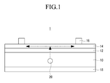
- Figure 1 is a partial cross-sectional schematic view of a solar cell according to an embodiment of the present invention.
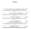
- Figure 2 is a flow chart schematically showing a process of manufacturing a solar cell according to an embodiment of the present invention.
- electrodes are disposed in the front of an emitter layer doped with impurities, and thus electrons are transferred to the emitter layer and collected in the electrodes. When the electrons are transferred to the electrodes, some electrons may be lost.
- the emitter layer should be doped with a high concentration of impurities to lessen its resistance, or in order to reduce the electron loss due to the transfer, intervals between the electrodes can be shorten to a range from about 1.5 mm to about 2 mm.
- a conductive transparent electrode layer having low resistance is disposed between the emitter layer and the electrodes, and thereby electrons are transferred through the conductive transparent electrode layer instead of the doped emitter layer.
- resistance loss can be reduced or minimized and light shading loss can be reduced since electrode intervals may be increased.
- Figure 1 is a partial cross-sectional schematic view of a solar cell 1 according to an embodiment of the present invention.
- the solar cell 1 includes a semiconductor substrate 10; an emitter layer 12 disposed on a first (or front) side of the semiconductor substrate 10; a conductive transparent electrode layer 14 disposed on the emitter layer 12; a first electrode 16 disposed on the conductive transparent electrode layer 14 and electrically connected to the conductive transparent electrode layer 14; and a second electrode 18 disposed on a second (or rear) side of the semiconductor substrate 10 and electrically connected to the semiconductor substrate 10.
- the semiconductor substrate 10 is a p-type silicon substrate doped with impurities of Group 3 elements such as B, Ga, Al, etc.
- the semiconductor substrate 10 can have various suitable concentrations of carriers (electrons or holes) produced by absorbing light depending on various specific resistances (doping concentration of impurities).
- the doping concentration also has an influence on recombination in which a carrier is not collected but is lost. Accordingly, when a semiconductor substrate is doped with impurities in a high concentration and thereby has small specific resistance, carriers produced by light absorption may have increased concentration and increased recombination, while when a semiconductor substrate is doped with impurities in a low concentration and thereby has large specific resistance, carriers produced by light absorption may have reduced concentration and decreased recombination. In other words, there is a trade-off between production of carriers and their loss due to recombination.
- a semiconductor substrate 10 doped with Group 3 elements may have specific resistance ranging from about 0.5 to about 3 ⁇ ⁇ cm (or from 0.5 to 3 ⁇ ⁇ cm).
- a semiconductor substrate has specific resistance of less than 0.5 ⁇ ⁇ cm, carriers produced by light absorption may have an increased concentration, but the recombination loss may be too high.
- a semiconductor substrate has specific resistance of more than 3 ⁇ ⁇ cm, a carrier produced by light absorption may have too low of a concentration even if recombination loss is lower.
- recombination loss when a semiconductor substrate has specific resistance of 0.5 ⁇ ⁇ cm, 1 ⁇ ⁇ cm, 1.5 ⁇ ⁇ cm, 2 ⁇ ⁇ cm, 2.5 ⁇ ⁇ cm, or 3 ⁇ ⁇ cm, recombination loss may be sufficiently reduce, thereby resulting in a high photoelectric efficiency of a cell.
- the emitter layer 12 is an n-type silicon substrate doped with impurities of Groups 5 elements such as P, As, Sb, etc.
- the semiconductor substrate 10 can be made of an n-type silicon substrate doped with P of Group 5.
- the emitter layer 12 may include a p-type silicon substrate doped with Group 3 elements.
- the semiconductor substrate 10 and the emitter layer 12 are doped by using a thermal diffusion process.
- This thermal diffusion contributes to fabrication of the semiconductor substrate 10 and the emitter layer 12 having a high doping concentration on the surface but progressively less concentration deeper inside the semiconductor substrate 10 and the emitter layer 12.
- the doping concentration profile can be generally measured by using secondary ion mass spectrometry (SIMS), but this takes a large amount of time and requires complicated analysis. Accordingly, the doping degree including doping concentration and depth can be evaluated by measuring surface resistance. The surface resistance has a decreasing value as doping becomes deeper with a higher concentration.
- the emitter layer 12 may appropriately have surface resistance of about 50 ⁇ / ⁇ or more (or not less than 50 ⁇ / ⁇ ) after doping the impurity.
- the emitter layer 12 may have surface resistance of less than 50 ⁇ / ⁇ , that is, a high doping concentration on the surface and deeper doping, it may have more loss due to recombination of a carrier excited by light.
- an emitter layer may have surface resistance ranging from 50 to 300 ⁇ / ⁇ .
- it may have surface resistance ranging from 50 to 150 ⁇ / ⁇ to reduce optical reflection loss due to decreased separation capability of a carrier and decreased area of a first electrode.
- the emitter layer 12 When the emitter layer 12 has surface resistance of 50 ⁇ / ⁇ , 80 ⁇ / ⁇ , 100 ⁇ / ⁇ , 150 ⁇ / ⁇ , 200 ⁇ / ⁇ , or 300 ⁇ / ⁇ after doping impurities, it may have reduced recombination loss of carriers exited by light, thereby resulting in a high photoelectric efficiency of a cell.
- the semiconductor substrate 10 contacts the emitter layer 12 and thereby forms p-n junctions.
- the emitter layer 12 includes a conductive transparent electrode layer 14 with low resistance thereon.
- the conductive transparent electrode layer 14 can be a passage for electrons and an anti-reflection film in a solar cell.
- the conductive transparent electrode layer 14 may have specific resistance of less than about 500 ⁇ ⁇ cm (when it is 100nm thick) or not greater than 500 ⁇ ⁇ cm (when it is 100nm thick). However, it can have specific resistance ranging from 100 to 500 ⁇ ⁇ cm according to another embodiment of the present invention.
- the conductive transparent electrode layer 14 has specific resistance of more than 500 ⁇ ⁇ cm, it may have a large loss during movement of electrons.
- the conductive transparent electrode layer 14 when the conductive transparent electrode layer 14 has specific resistance of 100 ⁇ ⁇ cm, 150 ⁇ ⁇ cm, 200 ⁇ ⁇ cm, 250 ⁇ ⁇ cm, 300 ⁇ ⁇ cm, 350 ⁇ ⁇ cm, 400 ⁇ ⁇ cm, 450 ⁇ ⁇ cm, or 500 ⁇ ⁇ cm, it may have reduced loss during movement of electrons, thereby resulting in a high photoelectric efficiency of a cell.
- the conductive transparent electrode layer 14 may have a lower specific resistance ( ) than that of the emitter layer 12.
- the conductive transparent electrode layer 14 may have a transmission rate of more than about 90% (or not less than 90%) for a wavelength ranging from about 350 to about 800nm (or from 350 to 800nm). However, according to another embodiment, it may have a transmission rate ranging from 90 to 99% for the wavelength ranging from about 350 to about 800nm (or from 350 to 800nm). When a conductive transparent electrode layer 14 has a transmission rate of less than 90% for the wavelength ranging from about 350 to about 800nm (or from 350 to 800nm), it may have a decreased amount of incident light.
- the conductive transparent electrode layer 14 When the conductive transparent electrode layer 14 has a transmission rate of 90%, 92%, 94%, 96%, 98%, or 99% for the wavelength ranging from about 350 to about 800nm (or from 350 to 800nm), it may have an increased amount of incident light, thereby resulting in a high photoelectric efficiency of a cell.
- the conductive transparent electrode layer 14 can be a passage for electrons, and also as an anti-reflection film.
- an anti-reflection film should simultaneously minimize (or reduce) reflection loss and recombination loss on the surface of a substrate. Accordingly, it may have a low absorption rate and refractive index, but a high transmission rate to minimize (or reduce) reflection loss. In addition, to minimize (or reduce) recombination loss on the surface, an anti-reflection film should have suitable refractive index, absorption yield, and surface passivation characteristics.
- the conductive transparent electrode layer 14 may have a refractive index ranging from about 1.7 to about 2.5 (or from 1.7 to 2.5). When a conductive transparent electrode layer 14 has a refractive index that is not within the above described range, it may cause a large reflection loss. On the contrary, when a conductive transparent electrode layer 14 has a refractive index of 1.7, 1.8, 1.9, 2.0, 2.1, 2.2, 2.3, 2.4, or 2.5, it may have a decreased reflection loss, thereby resulting in a high photoelectric efficiency of a cell.
- the conductive transparent electrode layer 14 may have various suitable thicknesses depending on its refractive index. Accordingly, considering the refractive index range, the conductive transparent electrode layer 14 may have a thickness ranging from about 60 to about 100nm (or from 60 to 100nm). When a conductive transparent electrode layer 14 is prepared to be out of the thickness range, it may cause a reflection loss. According to the embodiment of the present invention, when the conductive transparent electrode layer 14 has a thickness of 60nm, 70nm, 80nm, 90nm, or 100nm, it may have a reduced reflection loss, thereby resulting in a high photoelectric efficiency of a cell.
- the conductive transparent electrode layer 14 has a suitable refractive index and a suitable transmission rate for minimizing (or reducing) reflection loss.
- its reflection loss can be calculated by measuring its reflection rate.
- ultraviolet rays of the sun have a wavelength ranging from hundreds of nanometers to micrometers, while a silicon solar cell uses a wavelength ranging from 300 to 1100nm thereof.
- the conductive transparent electrode layer 14 may have various suitable refractive indexes depending on light wavelengths.
- a conductive transparent electrode layer has a particular refractive index at a particular wavelength, the thickness of the conductive transparent electrode layer 14 determines a suitable (or minimum) reflection rate at the wavelength. Accordingly, when a conductive transparent electrode layer 14 has a refractive index of 1.9 at a wavelength of 550nm where the sunlight is strongest, it may have a thickness of 90nm. On the other hand, when it has a refractive index of 2.3, it may have a thickness of 65nm.
- a conductive transparent electrode layer 14 has no particular limit as long as it is transparent and conductive.
- the conductive transparent electrode layer 14 may be formed from a material selected from the group consisting of indium tin oxide (ITO), a tin-based oxide (SnO 2 and the like), AgO, ZnO-(Ga 2 O 3 or Al 2 O 3 ), fluorine tin oxide (FTO), and mixtures thereof.
- First electrodes 16 are disposed on the conductive transparent electrode layer 14.
- the first electrodes 16 are electrically connected to the conductive transparent electrode layer 14 and disposed as a plurality of electrode parts with a particular distance therebetween.
- the disposition distance between the first electrodes 16 should be determined based on a trade-off relationship between resistance loss according to specific resistance of the conductive transparent electrode layer 14 and optical reflection loss due to electrode area. In other words, when the first electrodes 16 are disposed with a large distance therebetween, they may have a smaller area in total, thereby decreasing optical reflection loss.
- the first electrodes 16 may be disposed with a distance ranging from about 2.5 to about 8mm (or from 2.5 to 8mm) therebetween.
- the first electrodes 16 When the first electrodes 16 are disposed with a distance of less than 2.5mm therebetween, they may have an increased total area and thereby cause electrode shading loss.
- the first electrodes when they are disposed with a distance of more than 8mm therebetween, they may have a greater increase in resistance loss than a decrease in optical reflection as electrons need to move farther.
- the first electrodes are disposed with a distance of 2.5mm, 3mm, 4mm, 5mm, 6mm, 7mm, or 8mm therebetween, and thereby have decreased electrode shading loss, thereby resulting in a high photoelectric efficiency of a cell.
- the first electrodes when a conductive transparent electrode layer 14 has specific resistance of 100 ⁇ ⁇ cm, the first electrodes may be disposed with a distance ranging from 2.5 to 6mm therebetween.
- Each first electrode 16 may be formed from a material selected from the group consisting of Al, Ag, Ni, Cu, Ti, Pd, Cr, W, a conductive polymer, and combinations thereof.
- the material for forming one of the first electrodes 16 may be appropriately selected depending on its fabrication method.
- the first electrode 16 when screen printing is adopted, the first electrode 16 is prepared by using a material selected from the group consisting of Ag, Al, and combinations thereof.
- the first electrode 16 when an ink jet or dispensing method is adopted, the first electrode 16 may be prepared by using a material selected from the group consisting of Ni, Ag, and combinations thereof.
- the first electrode 16 is prepared by using a material selected from the group consisting of Ni, Cu, Ag, and combinations thereof, while when a deposition method is adopted, the first electrode 16 may be prepared by using a material selected from the group consisting of Al, Ni, Cu, Ag, Ti, Pd, Cr, W, and combinations thereof. Furthermore, when the first electrode 16 is prepared by firing at a low temperature, the first electrode 16 may include a mixture of Ag and a conductive polymer.
- a second electrode 18 is disposed on the back of the semiconductor substrate 10 and electrically connected thereto.
- the second electrode 18 may include the same (or substantially the same) material as the first electrodes 16.
- a solar cell according to an embodiment of the present invention may be manufactured by the following method: forming an emitter layer on a first (or front) side of a semiconductor substrate; forming a conductive transparent electrode layer on the emitter layer; forming first electrodes electrically connected to the conductive transparent electrode layer on the conductive transparent electrode layer; and forming a second electrode on a second (or rear) side of the semiconductor substrate.
- FIG 2 is a flow chart showing a process of manufacturing a solar cell according to an embodiment of the present invention. Referring to Figure 2 , the method is described in more detail hereinafter.
- an emitter layer is formed on a semiconductor substrate or on a first side of the semiconductor substrate (S1).
- the semiconductor substrate and the emitter layer are the same (or substantially the same) as described above with respect to Figure 1 .
- the semiconductor substrate can be pretreated with a process selected from the group consisting of a saw damage removal process, a texturing process by forming protrusions and depressions on the surface to reduce a surface reflection rate, and a substrate cleaning process before disposing the emitter layer on the semiconductor substrate.
- the emitter layer can be formed on the semiconductor substrate with a suitable method, for example, with a high temperature diffusion method.
- a suitable method for example, with a high temperature diffusion method.
- an oxidation film formed of phospho-silicate-glass (PSG) utilized in the case of P doping and disposed on the surface of the semiconductor substrate with a high temperature diffusion method may be removed by a chemical etching method.
- a conductive transparent electrode layer is disposed on the emitter layer (S2).
- the conductive transparent electrode layer may be the same (or substantially the same) as aforementioned.
- the conductive transparent electrode can be formed by coating a paste for forming a conductive transparent electrode layer and then heat-treating it, or with a deposition method by sputtering, plating, and the like.
- the paste may have somewhat different properties depending on the coating method.
- the coating method may include ink-jet printing, dispensing, spraying, a doctor blade method, screen printing, or the like.
- the transparent film can be formed with a spin-coating or spraying method or any suitable wet-coating method.
- a heat treatment after coating can be performed at a temperature ranging from 400 to 600°C for 30 minutes.
- the heat treatment can be performed at a temperature of less than 200°C.
- a first electrode is formed on the conductive transparent electrode layer and electrically connected thereto (S3).
- the first electrode is the same (or substantially the same) as aforementioned, and can be formed with a physical vapor deposition (PVD) method such as electroplating, sputtering, electron beam deposition, and the like.
- PVD physical vapor deposition
- the first electrode can be performed by coating a paste including a conductive material as the first electrode and then sintering it.
- p-n junctions are isolated in an edge-isolation (E/I) process.
- the edge-isolation (E/I) process is performed by using plasma after forming an emitter layer or by using a laser after forming a first electrode.
- a second electrode is disposed on a second (or back) side of the semiconductor substrate (S4).
- the second electrode is also the same (or substantially the same) as aforementioned, and can be formed with the same (or substantially the same) method as the first electrode.
- the aforementioned processes can be changed in order or performed together. For example, formation of a conductive transparent electrode layer (S2) can be exchanged with formation of the second electrode (S4). In addition, a paste can be patterned first and then sintered.
- a solar cell is the prepared (S5).
- the solar cell according to the aforementioned method can minimize (or reduce) resistance against electron movement and electrode shading loss, and thereby has a high photoelectric efficiency.
- an emitter layer can be doped with impurities at a low concentration, it can improve optical response characteristics and minimize (or reduce) recombination loss.
- formation of the first electrode S3 can be exchanged with formation of a second electrode S4, or they can be simultaneously (or concurrently) formed.
- An emitter layer was disposed to be 0.45 ⁇ m thick on one side of a boron-doped p-type silicon substrate (specific resistance: 1 ⁇ ⁇ cm) with phosphorus-doped n-type silicon.
- the boron was doped in an amount of 1.5X10 16 /cm 3 on a p-type silicon substrate.
- the emitter layer including n-type silicon had a surface resistance of 50 ⁇ / ⁇ .
- an 80nm-thick conductive transparent electrode layer was disposed on the emitter layer with a sputtering method.
- An Al-containing paste was screen-printed on the other side of the p-type silicon substrate (i.e., on the side having no emitter layer).
- the p-type silicon substrate with the conductive transparent electrode layer was screen-printed with a Ag-containing paste every 6mm to form a pattern, and thereafter sintered at 400°C for 30 seconds to simultaneously (or concurrently) form first and second electrodes to thereby fabricate a solar cell.
- the emitter layer in the corner of the solar cell was removed with a laser to separate it from the other side on the back of the substrate.
- a 0.3 ⁇ m-thick emitter layer was disposed with phosphorus-doped n-type silicon on one side of a boron-doped p-type silicon substrate (specific resistance: 1 ⁇ ⁇ cm).
- the boron was doped in an amount of 1.5X10 16 /cm 3 on the p-type silicon substrate.
- the emitter layer including n-type silicon had a surface resistance of 100 ⁇ / ⁇ .
- a conductive transparent electrode layer was disposed to be 80nm thick on the emitter layer by using indium tin oxide (ITO) with a sputtering method.
- ITO indium tin oxide
- an Al-containing paste was screen-printed on the other side of the p-type silicon substrate (i.e., on the side having no emitter layer).
- the p-type silicon substrate with the conductive transparent electrode layer was screen-printed with a Ag-containing paste every 2.5mm to form a pattern, and thereafter sintered at 400°C for 30 seconds to simultaneously (or concurrently) form first and second electrodes to thereby fabricate a solar cell.
- the emitter layer in the corner of the solar cell was removed with a laser to separate it from the other side on the back of the substrate.
- a 0.3 ⁇ m thick phosphorus-doped n-type silicon emitter layer was disposed on one side of a boron-doped p-type silicon substrate (specific resistance: 1 ⁇ ⁇ cm).
- the boron was doped in an amount of 1.5X10 16 /cm 3 on the p-type silicon substrate.
- the emitter layer including n-type silicon had surface resistance of 100 ⁇ / ⁇ .
- a conductive transparent electrode layer was disposed to be 80nm thick on the emitter layer by using indium tin oxide (ITO) with a sputtering method.
- ITO indium tin oxide
- An Al-containing paste was screen-printed on the other side of the p-type silicon substrate (i.e., on the side having no emitter layer).
- the p-type silicon substrate with the conductive transparent electrode layer was screen-printed with an Ag-containing paste every 6mm to form a pattern, and thereafter, sintered at 400°C for 30 seconds to simultaneously (or concurrently) form first and second electrodes to finally fabricate a solar cell.
- the emitter layer in the corner of the solar cell was removed with a laser to separate it from the other side on the back of the substrate.
- a 0.3 ⁇ m thick phosphorus-doped n-type silicon emitter layer was disposed on one side of a boron-doped p-type silicon substrate (specific resistance: 1 ⁇ ⁇ cm).
- the boron was doped in an amount of 1.5X10 16 /cm 3 on the p-type silicon substrate.
- the emitter layer including n-type silicon had surface resistance of 100 ⁇ / ⁇ .
- a conductive transparent electrode layer was disposed to be 80nm thick on the emitter layer by using indium tin oxide (ITO) with a sputtering method.
- ITO indium tin oxide
- An Al-containing paste was screen-printed on the other side of the p-type silicon substrate (i.e., on the side having no emitter layer).
- the p-type silicon substrate with the conductive transparent electrode layer was screen-printed with a Ag-containing paste at every 2.5mm intervals to form a pattern, and thereafter, sintered at 400°C for 30 seconds to simultaneously (or concurrently) form first and second electrodes to thereby fabricate a solar cell.
- the emitter layer in the corner of the solar cell was removed with a laser to separate it from the other side on the back of the substrate.
- a solar cell was fabricated according to the same (or substantially the same) method as in Example 4, except for disposing a 100nm-thick conductive transparent electrode layer with AZO (Al doped ZnO) as a material for a conductive transparent electrode layer with a sputtering method.
- AZO Al doped ZnO
- a solar cell was fabricated according to the same (or substantially the same) method as in Example 4, except for disposing a 100nm-thick conductive transparent electrode layer with SnO 2 by spin-coating a SnO 2 -containing solution on the emitter layer and then heat-treating it at 700°C.
- a solar cell was fabricated according to the same (or substantially the same) method as in Example 3, except for using FTO as a material for forming a conductive transparent electrode layer.
- a solar cell was fabricated according to the same (or substantially the same) method as in Example 3, except for using AgO as a material for forming a conductive transparent electrode layer.
- a 0.45 ⁇ m thick phosphorus-doped n-type silicon emitter layer was disposed on one side of a boron-doped p-type silicon substrate (specific resistance: 1 ⁇ ⁇ cm).
- the boron was doped in an amount of 1.5X10 16 /cm 3 on the p-type silicon substrate.
- the emitter layer including n-type silicon had surface resistance of 50 ⁇ / ⁇ .
- a 70nm-thick anti-reflection film was disposed on the emitter layer by using silicon nitride (SiN x ) with a refractive index of 2.1 with a chemical vapor deposition method.
- An Al-containing paste was screen-printed on the other side of the p-type silicon substrate (i.e., on the side having no emitter layer).
- the p-type silicon substrate with the conductive transparent electrode layer was screen-printed with a Ag-containing paste every 2.5mm to form a pattern, and thereafter, sintered at 400°C for 30 seconds to simultaneously (or concurrently) form first and second electrodes to thereby fabricate a solar cell.
- the emitter layer in the corner of the solar cell was removed with a laser to separate it from the other side on the back of the substrate.
- the solar cell conductive transparent electrode layers according to Examples 1 to 5 were measured regarding thickness, specific resistance, transmission rate, and refractive index. The results are shown in the following Table 1.
- Table 1 Thickness (nm) Specific resistance ( ⁇ ⁇ cm) Transmission rate (%, at 600nm) Refractive index (at 600nm)
- Example 1 80 150 95 1.9
- Example 2 80 150 95 1.9
- Example 3 80 150 95 1.9
- Example 4 100 140 95 1.8
- Example 5 100 452 92 1.9
- the solar cells according to Examples 1 to 3 showed better open circuit voltage (VOC), short-circuit current density (JSC), fill factor (FF), and efficiency ( ⁇ W) of white light as compared to the solar cell of Comparative Example 1.
- Example 1 included widely-patterned electrodes and thereby had less optical reflection loss.
- the solar cell of Example 2 had increased surface resistance in the emitter layer, and thereby had less recombination loss of a carrier excited by light.
- the solar cell of Example 3 had both less optical reflection loss and less recombination loss of a carrier excited by light.
- the solar cells of Examples 1 to 3 had better photoelectric efficiency as compared to that of Comparative Example 1.
- the solar cells of Examples 4 to 8 were measured regarding open circuit voltage (V OC ), short-circuit current density (J SC ), fill factor (FF), and efficiency ( ⁇ ) of white light according to the same (or substantially the same) method as aforementioned.
- the solar cells according to Example 4 to 6 had equivalent values to that of Example 2 due to increased surface resistances in the emitter layers and reduced recombination loss of a carrier excited by light.
- the solar cells of Examples 7 and 8 had equivalent values to that of Example 3 due to reduced reflection loss and reduced recombination loss of a carrier excited by light.
- a solar cell of an embodiment of the present invention has a high photoelectric efficiency by minimizing (or reducing) electron transfer resistance and electrode shading loss.
- the emitter layer may be doped with a low concentration of impurities, and thereby can improve an optical response at a short wavelength and minimize (or reduce) recombination loss.
Landscapes
- Photovoltaic Devices (AREA)
Applications Claiming Priority (1)
| Application Number | Priority Date | Filing Date | Title |
|---|---|---|---|
| KR1020070070681A KR20090007063A (ko) | 2007-07-13 | 2007-07-13 | 태양전지 및 이의 제조방법 |
Publications (1)
| Publication Number | Publication Date |
|---|---|
| EP2015365A2 true EP2015365A2 (de) | 2009-01-14 |
Family
ID=39789504
Family Applications (1)
| Application Number | Title | Priority Date | Filing Date |
|---|---|---|---|
| EP08101840A Withdrawn EP2015365A2 (de) | 2007-07-13 | 2008-02-21 | Solarzelle mit einer transparenten Elektrode und Verfahren zu seiner Herstellung |
Country Status (5)
| Country | Link |
|---|---|
| US (1) | US20090120494A1 (de) |
| EP (1) | EP2015365A2 (de) |
| JP (1) | JP2009021541A (de) |
| KR (1) | KR20090007063A (de) |
| CN (1) | CN101345265A (de) |
Cited By (1)
| Publication number | Priority date | Publication date | Assignee | Title |
|---|---|---|---|---|
| WO2011120103A1 (en) * | 2010-04-01 | 2011-10-06 | The University Of Melbourne | Dye-sensitised solar cell with nickel cathode |
Families Citing this family (17)
| Publication number | Priority date | Publication date | Assignee | Title |
|---|---|---|---|---|
| KR100993511B1 (ko) | 2008-11-19 | 2010-11-12 | 엘지전자 주식회사 | 태양 전지 및 그 제조 방법 |
| KR101145928B1 (ko) * | 2009-03-11 | 2012-05-15 | 엘지전자 주식회사 | 태양 전지 및 태양 전지의 제조 방법 |
| KR101080344B1 (ko) | 2009-09-03 | 2011-11-04 | 성균관대학교산학협력단 | 태양전지의 선택적 에미터 형성방법 및 태양전지의 제조방법 |
| EP2312641A1 (de) * | 2009-10-13 | 2011-04-20 | Ecole Polytechnique Fédérale de Lausanne (EPFL) | Vorrichtung mit elektrischen Kontakten und deren Herstellungsverfahren |
| KR101410392B1 (ko) * | 2009-12-30 | 2014-06-20 | 주성엔지니어링(주) | 이종 접합 태양전지 및 그 제조방법 |
| KR101676750B1 (ko) * | 2010-07-28 | 2016-11-17 | 주성엔지니어링(주) | 기판형 태양전지 및 그 제조방법 |
| KR101733055B1 (ko) * | 2010-09-06 | 2017-05-24 | 엘지전자 주식회사 | 태양 전지 모듈 |
| JP5893251B2 (ja) * | 2011-02-11 | 2016-03-23 | 三菱マテリアル株式会社 | 太陽電池用複合膜の製造方法 |
| FR2972298B1 (fr) * | 2011-03-04 | 2015-07-31 | Commissariat Energie Atomique | Procede de metallisation de surfaces texturees |
| JP2012209525A (ja) * | 2011-03-30 | 2012-10-25 | Mitsubishi Materials Corp | 太陽電池向け透明導電膜用組成物および透明導電膜 |
| US20130319502A1 (en) * | 2012-05-31 | 2013-12-05 | Aqt Solar, Inc. | Bifacial Stack Structures for Thin-Film Photovoltaic Cells |
| CN111048972A (zh) * | 2012-07-30 | 2020-04-21 | 工业研究与发展基金会有限公司 | 太阳能系统、使用太阳能的方法、用于发电的方法和设备 |
| US20140053895A1 (en) * | 2012-08-24 | 2014-02-27 | Rosestreet Labs, Llc | Intentionally-doped cadmium oxide layer for solar cells |
| US9202959B2 (en) * | 2012-09-25 | 2015-12-01 | International Business Machines Corporation | Embedded junction in hetero-structured back-surface field for photovoltaic devices |
| CN104253178A (zh) * | 2013-06-26 | 2014-12-31 | 联景光电股份有限公司 | 太阳能电池及其制造方法 |
| CN104752528A (zh) * | 2013-12-27 | 2015-07-01 | 比亚迪股份有限公司 | 一种太阳能电池片及其制备方法、含有该电池片的太阳能电池组件 |
| CN116259679B (zh) | 2021-12-09 | 2026-05-01 | 浙江晶科能源有限公司 | 太阳能电池及光伏组件 |
Family Cites Families (12)
| Publication number | Priority date | Publication date | Assignee | Title |
|---|---|---|---|---|
| CA918297A (en) * | 1969-09-24 | 1973-01-02 | Tanimura Shigeru | Semiconductor device and method of making |
| US4431858A (en) * | 1982-05-12 | 1984-02-14 | University Of Florida | Method of making quasi-grain boundary-free polycrystalline solar cell structure and solar cell structure obtained thereby |
| GB2185758B (en) * | 1985-12-28 | 1990-09-05 | Canon Kk | Method for forming deposited film |
| US4927770A (en) * | 1988-11-14 | 1990-05-22 | Electric Power Research Inst. Corp. Of District Of Columbia | Method of fabricating back surface point contact solar cells |
| US5030295A (en) * | 1990-02-12 | 1991-07-09 | Electric Power Research Institut | Radiation resistant passivation of silicon solar cells |
| JP2918345B2 (ja) * | 1991-02-20 | 1999-07-12 | キヤノン株式会社 | 光起電力素子 |
| US5380371A (en) * | 1991-08-30 | 1995-01-10 | Canon Kabushiki Kaisha | Photoelectric conversion element and fabrication method thereof |
| US5907766A (en) * | 1996-10-21 | 1999-05-25 | Electric Power Research Institute, Inc. | Method of making a solar cell having improved anti-reflection passivation layer |
| KR100790956B1 (ko) * | 2000-10-06 | 2008-01-03 | 신에쯔 한도타이 가부시키가이샤 | 태양전지 및 그 제조방법 |
| JP3679771B2 (ja) * | 2002-03-19 | 2005-08-03 | 三洋電機株式会社 | 光起電力装置、及び光起電力装置の製造方法 |
| EP1548868A4 (de) * | 2002-10-03 | 2009-08-12 | Fujikura Ltd | ELEKTRODENSUBSTRAT, FOTOELEKTRISCHES UMSETZUNGSELEMENT, LEITFûHIGES GLASSUBSTRAT UND HERSTELLUNGSVERFAHREN DAF R UND PIGMENTSENSIBILISIERUNGSSOLARZELLE |
| JP2006183117A (ja) * | 2004-12-28 | 2006-07-13 | Showa Shell Sekiyu Kk | MOCVD(有機金属化学蒸着)法によるZnO系透明導電膜の製造方法 |
-
2007
- 2007-07-13 KR KR1020070070681A patent/KR20090007063A/ko not_active Ceased
-
2008
- 2008-02-01 CN CNA200810006083XA patent/CN101345265A/zh active Pending
- 2008-02-05 JP JP2008024981A patent/JP2009021541A/ja active Pending
- 2008-02-21 EP EP08101840A patent/EP2015365A2/de not_active Withdrawn
- 2008-02-22 US US12/036,118 patent/US20090120494A1/en not_active Abandoned
Cited By (1)
| Publication number | Priority date | Publication date | Assignee | Title |
|---|---|---|---|---|
| WO2011120103A1 (en) * | 2010-04-01 | 2011-10-06 | The University Of Melbourne | Dye-sensitised solar cell with nickel cathode |
Also Published As
| Publication number | Publication date |
|---|---|
| CN101345265A (zh) | 2009-01-14 |
| KR20090007063A (ko) | 2009-01-16 |
| JP2009021541A (ja) | 2009-01-29 |
| US20090120494A1 (en) | 2009-05-14 |
Similar Documents
| Publication | Publication Date | Title |
|---|---|---|
| US20090120494A1 (en) | Solar cell and method of manufacturing the same | |
| EP2353187B1 (de) | Solarzelle und herstellungsverfahren dafür | |
| KR101142861B1 (ko) | 태양 전지 및 그 제조 방법 | |
| US10847663B2 (en) | Solar cell and method for manufacturing the same | |
| EP2765615B1 (de) | Solarzelle, herstellungsverfahren für die solarzelle und solarzellenmodul | |
| EP2110859B1 (de) | Fotoelektrischer wandler des laminattyps und verfahren zu seiner herstellung | |
| US9508875B2 (en) | Solar cell and method for manufacturing the same | |
| EP2711988B1 (de) | Solarzelle und Verfahren zu ihrer Herstellung | |
| KR100946797B1 (ko) | 레이저를 이용한 고효율 태양전지의 제조방법 | |
| WO2013172056A1 (ja) | 光電変換装置およびその製造方法、光電変換モジュール | |
| US20110180122A1 (en) | Floating grid module design for thin film silicon solar cells | |
| EP3206233A1 (de) | Solarzelle und verfahren zur herstellung davon | |
| KR20170024103A (ko) | 태양 전지 | |
| EP2426722A2 (de) | Solarzellenmodul | |
| US20120048360A1 (en) | Solar cell and method of manufacturing the same | |
| US8927854B2 (en) | Solar cell and method for manufacturing the same | |
| KR101155890B1 (ko) | 태양 전지 및 그 제조 방법 | |
| KR20210044987A (ko) | 태양 전지 및 이의 제조 방법 | |
| EP2579323A1 (de) | Zwischenschicht für eine photoelektrische laminatwandlervorrichtung, photoelektrische laminatwandlervorrichtung und verfahren zur herstellung der photoelektrischen laminatwandlervorrichtung | |
| KR101406955B1 (ko) | 태양전지 및 그 제조방법 | |
| EP4174914B1 (de) | Tandemsolarzelle | |
| KR101766339B1 (ko) | 태양 전지 및 그 제조 방법 | |
| KR101072531B1 (ko) | 태양전지 및 그 제조방법 | |
| KR20210065908A (ko) | 태양전지 및 태양전지의 제조방법 | |
| KR20100082607A (ko) | 태양 전지 및 그 제조 방법 |
Legal Events
| Date | Code | Title | Description |
|---|---|---|---|
| PUAI | Public reference made under article 153(3) epc to a published international application that has entered the european phase |
Free format text: ORIGINAL CODE: 0009012 |
|
| 17P | Request for examination filed |
Effective date: 20080221 |
|
| AK | Designated contracting states |
Kind code of ref document: A2 Designated state(s): AT BE BG CH CY CZ DE DK EE ES FI FR GB GR HR HU IE IS IT LI LT LU LV MC MT NL NO PL PT RO SE SI SK TR |
|
| AX | Request for extension of the european patent |
Extension state: AL BA MK RS |
|
| RAP1 | Party data changed (applicant data changed or rights of an application transferred) |
Owner name: SAMSUNG SDI CO., LTD. |
|
| STAA | Information on the status of an ep patent application or granted ep patent |
Free format text: STATUS: THE APPLICATION HAS BEEN WITHDRAWN |
|
| 18W | Application withdrawn |
Effective date: 20130530 |