EP2009783A1 - Local oscillator, reception device and electronic device using the same - Google Patents
Local oscillator, reception device and electronic device using the same Download PDFInfo
- Publication number
- EP2009783A1 EP2009783A1 EP08720373A EP08720373A EP2009783A1 EP 2009783 A1 EP2009783 A1 EP 2009783A1 EP 08720373 A EP08720373 A EP 08720373A EP 08720373 A EP08720373 A EP 08720373A EP 2009783 A1 EP2009783 A1 EP 2009783A1
- Authority
- EP
- European Patent Office
- Prior art keywords
- variable
- capacitive element
- variable capacitance
- reference voltage
- circuit
- Prior art date
- Legal status (The legal status is an assumption and is not a legal conclusion. Google has not performed a legal analysis and makes no representation as to the accuracy of the status listed.)
- Withdrawn
Links
Images


Classifications
-
- H—ELECTRICITY
- H03—ELECTRONIC CIRCUITRY
- H03L—AUTOMATIC CONTROL, STARTING, SYNCHRONISATION, OR STABILISATION OF GENERATORS OF ELECTRONIC OSCILLATIONS OR PULSES
- H03L7/00—Automatic control of frequency or phase; Synchronisation
- H03L7/06—Automatic control of frequency or phase; Synchronisation using a reference signal applied to a frequency- or phase-locked loop
- H03L7/08—Details of the phase-locked loop
- H03L7/085—Details of the phase-locked loop concerning mainly the frequency- or phase-detection arrangement including the filtering or amplification of its output signal
- H03L7/087—Details of the phase-locked loop concerning mainly the frequency- or phase-detection arrangement including the filtering or amplification of its output signal using at least two phase detectors or a frequency and phase detector in the loop
-
- H—ELECTRICITY
- H03—ELECTRONIC CIRCUITRY
- H03B—GENERATION OF OSCILLATIONS, DIRECTLY OR BY FREQUENCY-CHANGING, BY CIRCUITS EMPLOYING ACTIVE ELEMENTS WHICH OPERATE IN A NON-SWITCHING MANNER; GENERATION OF NOISE BY SUCH CIRCUITS
- H03B5/00—Generation of oscillations using amplifier with regenerative feedback from output to input
- H03B5/08—Generation of oscillations using amplifier with regenerative feedback from output to input with frequency-determining element comprising lumped inductance and capacitance
- H03B5/12—Generation of oscillations using amplifier with regenerative feedback from output to input with frequency-determining element comprising lumped inductance and capacitance active element in amplifier being semiconductor device
- H03B5/1206—Generation of oscillations using amplifier with regenerative feedback from output to input with frequency-determining element comprising lumped inductance and capacitance active element in amplifier being semiconductor device using multiple transistors for amplification
- H03B5/1212—Generation of oscillations using amplifier with regenerative feedback from output to input with frequency-determining element comprising lumped inductance and capacitance active element in amplifier being semiconductor device using multiple transistors for amplification the amplifier comprising a pair of transistors, wherein an output terminal of each being connected to an input terminal of the other, e.g. a cross coupled pair
- H03B5/1215—Generation of oscillations using amplifier with regenerative feedback from output to input with frequency-determining element comprising lumped inductance and capacitance active element in amplifier being semiconductor device using multiple transistors for amplification the amplifier comprising a pair of transistors, wherein an output terminal of each being connected to an input terminal of the other, e.g. a cross coupled pair the current source or degeneration circuit being in common to both transistors of the pair, e.g. a cross-coupled long-tailed pair
-
- H—ELECTRICITY
- H03—ELECTRONIC CIRCUITRY
- H03B—GENERATION OF OSCILLATIONS, DIRECTLY OR BY FREQUENCY-CHANGING, BY CIRCUITS EMPLOYING ACTIVE ELEMENTS WHICH OPERATE IN A NON-SWITCHING MANNER; GENERATION OF NOISE BY SUCH CIRCUITS
- H03B5/00—Generation of oscillations using amplifier with regenerative feedback from output to input
- H03B5/08—Generation of oscillations using amplifier with regenerative feedback from output to input with frequency-determining element comprising lumped inductance and capacitance
- H03B5/12—Generation of oscillations using amplifier with regenerative feedback from output to input with frequency-determining element comprising lumped inductance and capacitance active element in amplifier being semiconductor device
- H03B5/1231—Generation of oscillations using amplifier with regenerative feedback from output to input with frequency-determining element comprising lumped inductance and capacitance active element in amplifier being semiconductor device the amplifier comprising one or more bipolar transistors
-
- H—ELECTRICITY
- H03—ELECTRONIC CIRCUITRY
- H03B—GENERATION OF OSCILLATIONS, DIRECTLY OR BY FREQUENCY-CHANGING, BY CIRCUITS EMPLOYING ACTIVE ELEMENTS WHICH OPERATE IN A NON-SWITCHING MANNER; GENERATION OF NOISE BY SUCH CIRCUITS
- H03B5/00—Generation of oscillations using amplifier with regenerative feedback from output to input
- H03B5/08—Generation of oscillations using amplifier with regenerative feedback from output to input with frequency-determining element comprising lumped inductance and capacitance
- H03B5/12—Generation of oscillations using amplifier with regenerative feedback from output to input with frequency-determining element comprising lumped inductance and capacitance active element in amplifier being semiconductor device
- H03B5/1237—Generation of oscillations using amplifier with regenerative feedback from output to input with frequency-determining element comprising lumped inductance and capacitance active element in amplifier being semiconductor device comprising means for varying the frequency of the generator
- H03B5/1262—Generation of oscillations using amplifier with regenerative feedback from output to input with frequency-determining element comprising lumped inductance and capacitance active element in amplifier being semiconductor device comprising means for varying the frequency of the generator the means comprising switched elements
- H03B5/1265—Generation of oscillations using amplifier with regenerative feedback from output to input with frequency-determining element comprising lumped inductance and capacitance active element in amplifier being semiconductor device comprising means for varying the frequency of the generator the means comprising switched elements switched capacitors
-
- H—ELECTRICITY
- H03—ELECTRONIC CIRCUITRY
- H03L—AUTOMATIC CONTROL, STARTING, SYNCHRONISATION, OR STABILISATION OF GENERATORS OF ELECTRONIC OSCILLATIONS OR PULSES
- H03L7/00—Automatic control of frequency or phase; Synchronisation
- H03L7/06—Automatic control of frequency or phase; Synchronisation using a reference signal applied to a frequency- or phase-locked loop
- H03L7/08—Details of the phase-locked loop
- H03L7/099—Details of the phase-locked loop concerning mainly the controlled oscillator of the loop
-
- H—ELECTRICITY
- H03—ELECTRONIC CIRCUITRY
- H03L—AUTOMATIC CONTROL, STARTING, SYNCHRONISATION, OR STABILISATION OF GENERATORS OF ELECTRONIC OSCILLATIONS OR PULSES
- H03L7/00—Automatic control of frequency or phase; Synchronisation
- H03L7/06—Automatic control of frequency or phase; Synchronisation using a reference signal applied to a frequency- or phase-locked loop
- H03L7/16—Indirect frequency synthesis, i.e. generating a desired one of a number of predetermined frequencies using a frequency- or phase-locked loop
- H03L7/18—Indirect frequency synthesis, i.e. generating a desired one of a number of predetermined frequencies using a frequency- or phase-locked loop using a frequency divider or counter in the loop
-
- H—ELECTRICITY
- H03—ELECTRONIC CIRCUITRY
- H03B—GENERATION OF OSCILLATIONS, DIRECTLY OR BY FREQUENCY-CHANGING, BY CIRCUITS EMPLOYING ACTIVE ELEMENTS WHICH OPERATE IN A NON-SWITCHING MANNER; GENERATION OF NOISE BY SUCH CIRCUITS
- H03B2201/00—Aspects of oscillators relating to varying the frequency of the oscillations
- H03B2201/02—Varying the frequency of the oscillations by electronic means
- H03B2201/0208—Varying the frequency of the oscillations by electronic means the means being an element with a variable capacitance, e.g. capacitance diode
-
- H—ELECTRICITY
- H03—ELECTRONIC CIRCUITRY
- H03B—GENERATION OF OSCILLATIONS, DIRECTLY OR BY FREQUENCY-CHANGING, BY CIRCUITS EMPLOYING ACTIVE ELEMENTS WHICH OPERATE IN A NON-SWITCHING MANNER; GENERATION OF NOISE BY SUCH CIRCUITS
- H03B2201/00—Aspects of oscillators relating to varying the frequency of the oscillations
- H03B2201/02—Varying the frequency of the oscillations by electronic means
- H03B2201/025—Varying the frequency of the oscillations by electronic means the means being an electronic switch for switching in or out oscillator elements
-
- H—ELECTRICITY
- H03—ELECTRONIC CIRCUITRY
- H03J—TUNING RESONANT CIRCUITS; SELECTING RESONANT CIRCUITS
- H03J2200/00—Indexing scheme relating to tuning resonant circuits and selecting resonant circuits
- H03J2200/10—Tuning of a resonator by means of digitally controlled capacitor bank
-
- H—ELECTRICITY
- H03—ELECTRONIC CIRCUITRY
- H03L—AUTOMATIC CONTROL, STARTING, SYNCHRONISATION, OR STABILISATION OF GENERATORS OF ELECTRONIC OSCILLATIONS OR PULSES
- H03L2207/00—Indexing scheme relating to automatic control of frequency or phase and to synchronisation
- H03L2207/06—Phase locked loops with a controlled oscillator having at least two frequency control terminals
Definitions
- the present invention relates to local oscillators, and receivers and electronic devices using a local oscillator.
- FIG. 9 A conventional local oscillator disclosed in Patent Document 1 is described with reference to Fig. 9 .
- conventional oscillator 10 includes oscillation circuit 2 and resonance circuit 30 connected to this oscillation circuit 2.
- Oscillation circuit 2 and resonance circuit 30 are connected in a loop with PLL circuit 60.
- Resonance circuit 30 includes inductor elements 20a and 20b connected to oscillation circuit 2. Inductor elements 20a and 20b are connected in series, and their contact point is connected to VCC. Resonance circuit 30 includes first variable capacitance section 330 connected in parallel to inductor elements 20a and 20b, and second variable capacitance section 430 connected in parallel to this first variable capacitance section 330. First variable capacitance section 330 is connected in parallel to inductor elements 20a and 20b, and includes variable capacitive elements 310a and 310b that change a capacity value based on control voltage supplied from control voltage input terminal 35 and reference voltage V REF supplied from reference voltage supply 500, and capacitive elements 311a and 311b connected in series to this variable capacitive element 310.
- Variable capacitive elements 310a and 310b are connected in series, and their contact point is connected to reference voltage supply 500.
- Variable capacitive element 310a and capacitive element 311a, and variable capacitive element 310b and capacitive element 311a are connected in series, respectively. Their contact points are connected to control voltage input terminal 35.
- Variable capacitive element 310a and capacitive element 311a, and variable capacitive element 310b and capacitive element 311b configure variable capacitance circuits 31a and 31b, respectively.
- Second variable capacitance section 430 includes first capacitance switch circuits 41a and 41b connected in parallel to inductor elements 20a and 20b, and second capacitance switch circuits 42a and 42b connected in parallel to these first capacitance switch circuits 41a and 41b.
- First capacitance switch circuit 41a includes capacitive element 410a and first switch 411a connected in series to this capacitive element 410a. This first switch 411a is switched between on and off by a signal supplied from first capacitance control terminal 413.
- first capacitance switch circuit 41b includes capacitive element 410b and first switch 411b connected in series to this capacitive element 410b.
- This first switch 411b is switched on and off by a signal supplied from first capacitance control terminal 413.
- First switches 411a and 411b are connected in series, and their contact point is connected to GND.
- Second capacitance switch circuit 42a includes capacitive element 420a and second switch 421a connected in series to this capacitive element 420a.
- This second switch 21a is switched between on and off by a signal supplied from second capacitance control terminal 423.
- second capacitance switch circuit 42b includes capacitive element 420b and second switch 421b connected in series to this capacitive element 420b.
- This second switch 421b is switched between on and off by a signal supplied from second capacitance control terminal 423.
- Second switches 421a and 421b are connected in series, and their contact point is connected to GND.
- the frequency of the oscillation signal from local oscillator 10 is the resonance frequency of resonance circuit 30.
- This resonance frequency is determined by first variable capacitance section 330, second variable capacitance section 430, and inductors 20a and 20b.
- the capacity values of variable capacitive elements 310a and 310b provided in first variable capacitance section 330 are determined by the reference voltage supplied from reference voltage supply 500 and the control voltage supplied from control voltage input terminal 35.
- the capacity value of second variable capacitance section 430 is determined by how many of capacitive elements 410a and 410b and capacitive elements 420a and 420b are connected in parallel by the on-and-off combination of first switches 411a and 411b and second switches 421a and 421b.
- a control signal output from frequency-adjusting circuit 670 of PLL 600 is used for controlling first switches 411a and 411b and second switches 421a and 421b.
- This frequency-adjusting circuit 670 compares the frequency difference between output signal f DIV of oscillation-frequency divider 610 and output signal f REF of reference-frequency divider 630, and determines a capacity value that minimizes the frequency difference between f DIV and F REF .
- Frequency-adjusting circuit 670 then examines the combination of capacitive elements 410a and 410b and capacitive elements 420a and 420b, and controls first switches 411a and 411b and second switches 421a and 421b via first and second capacitance control terminals 413 and 423. This structure achieves a broad oscillation frequency range.
- Fig. 10 is a graph illustrating frequency characteristic, which shows the relationship between first variable capacitance control voltage (V T ) applied to control voltage input terminal 35 and oscillation frequency (fosc) of local oscillator 10 in Fig. 9 .
- Bands 1 to 4 show the characteristic of V T vs. fosc when first switches 411a and 411b and second switches 421a and 421b are turned on and off in four combinations.
- the capacity value of second variable capacitance section 430 becomes capacity value C SW1 of capacitive element 410a or 410b, or capacity value C SW2 of capacitive element 420a or 420b. If the capacity values of capacitive elements 410a and 410b and capacitive elements 420a and 420b are C SW1 > C SW2 , the characteristic of Band 2 is that only first switches 411a and 411b are turned on, and the characteristic of Band 3 is that only second switches 421a and 421b are turned on.
- Oscillation frequencies f OSC1 to f OSC4 of Bands 1 to 4 are expressed by Formulae 1 to 4.
- Formula 2 f OSC ⁇ 2 1 2 ⁇ ⁇ ⁇ L ( C
- Frequency control sensitivity df OSC1 /dV T to df OSC4 /dV T which are gradients of V T vs. f OSC in bands 1 to 4 are expressed by the following formulae 5 to 8.
- Formula 5 df OSC ⁇ 1 / dV T - ⁇ ⁇ C ⁇ 1 2 4 ⁇ ⁇ ⁇ L ⁇ C ⁇ 1 + ⁇ ⁇ V T + ⁇ ⁇ 3 2 ⁇ C SW ⁇ 1 ⁇ C ⁇ 1 + ⁇ ⁇ V T + ⁇ + C ⁇ 1 ⁇ ⁇ ⁇ V T + ⁇ 3 2
- Formula 6 df OSC ⁇ 2 / dV T - ⁇ ⁇ C ⁇ 1 2 4 ⁇ ⁇ ⁇ L ⁇ C ⁇ 1 + ⁇ ⁇ V T + ⁇ ⁇ C SW ⁇ 1 ⁇ C ⁇ 1 + ⁇ ⁇ V T + ⁇ + C ⁇ 1 ⁇ ⁇ ⁇ V T + ⁇ 3 2 df
- the frequency control sensitivity which is a gradient of V T vs. f OSC of bands 1 to 4
- fosc fluctuates by voltage noise superimposed on control voltage V T , and thus a phase noise of local oscillator 10 degrades.
- a local oscillator with next features are demanded: A broad oscillation frequency range for handling multiple divided frequency bands, and good phase noise characteristic that does not degrade a bit-error rate even if signals are phase-modulated to multiple values for achieving high-quality image, sound, and data.
- Patent Document Japanese Patent No. 3488180
- the present invention solves these disadvantages, and offers a local oscillator that can achieve both a broad oscillation frequency range and good phase noise characteristic.
- the local oscillator of the present invention includes an oscillation circuit and a resonance circuit connected to this oscillation circuit.
- This resonance circuit includes an inductor element connected to the oscillation circuit, a first variable capacitance section connected to this inductor element, and a second variable capacitance section connected in parallel to this first variable capacitance section:
- the first variable capacitance section includes a first variable capacitive element connected to the inductor element, and a second variable capacitive element connected in parallel to this first variable capacitive element.
- the first variable capacitive element changes its capacity value based on control voltage and first reference voltage
- the second variable capacitive element changes its capacity value based on the control voltage and second reference voltage.
- the first reference voltage and the second reference voltage are controlled based on the capacity value of the second variable capacitance section.
- the present invention decreases a frequency control sensitivity of the local oscillator in high oscillation-frequency bands by providing multiple variable capacitive elements to which different reference voltages can be set, and switching these reference voltages.
- This offers substantially constant frequency control sensitivity within the entire oscillation-frequency range of the local oscillator. Accordingly, the phase noise characteristic can be improved over the broad frequency range.
- the local oscillator of the present invention is employed in configuring a receiver such as a tuner, or an electronic device for communications system, broadcast standards with a broad frequency range and communications standards with different frequency bands can be supported.
- good phase noise characteristic achieves transmission and reception of high-quality images, sound, and data.
- Fig. 1 is a block diagram of a local oscillator in this exemplary embodiment.
- local oscillator 1 includes oscillation circuit 2 and resonance circuit 3 connected to this oscillation circuit 2.
- Oscillation circuit 2 and resonance circuit 3 are connected in a loop with PLL circuit 60.
- a receiver (not illustrated) employing this local oscillator 1 includes a mixer (not illustrated) for converting a received signal to a intermediate-frequency signal using a local signal output from local oscillation signal output terminals 18a and 18b of local oscillator 1, and a demodulator (not illustrated) for demodulating an intermediate-frequency signal output from this mixer.
- An electronic device (not illustrated) employing this local oscillator 1 includes a signal processor connected to an output side of this demodulator, and a display unit (not illustrated) such as a liquid crystal display or a sound playback unit (not illustrated) such as a speaker.
- a display unit such as a liquid crystal display or a sound playback unit (not illustrated) such as a speaker.
- Resonance circuit 3 includes inductor elements 20a and 20b connected to oscillation circuit 2. Inductor elements 20a and 20b are connected in series, and their contact point is connected to VCC. Resonance circuit 3 further includes first variable capacitance section 33 and second variable capacitance section 430 that are connected in parallel to this first variable capacitance section 33.
- First variable capacitance section 33 includes first variable capacitance circuits 31a and 31b and second variable capacitance circuits 32a and 32b that are connected in parallel to inductor elements 20a and 20b.
- First variable capacitance circuits 31a and 31b include variable capacitive elements (first variable capacitive elements) 310a and 310b for changing the capacity value based on control voltage V T supplied from control voltage input terminal 35 and first reference voltage V REF1 supplied from first reference-voltage generating circuit 6 via first reference voltage terminal 312.
- First variable capacitance circuits 31a and 31b also include capacitive elements (first capacitive elements) 311a and 311b that are connected in series to variable capacitive elements 310a and 310b.
- Variable capacitive elements 310a and 310b are connected in series, and their contact point is connected to first reference voltage terminal 312.
- variable capacitive element 310b and capacitive element 311b are connected in series, and their contact point is connected to control voltage input terminal 35.
- Capacitive elements 311a and 311b gavlanically separates voltage applied from VCC via inductor elements 20a and 20b and voltage applied from control voltage input terminal 35 via variable capacitive elements 310a and 310b, respectively.
- Second variable capacitance circuits 32a and 32b include variable capacitive elements (second variable capacitive elements) 320a and 320b that change their capacity values based on control voltage V T supplied from control voltage input terminal 35 and second reference voltage V REF2 supplied from second reference-voltage generating circuit 7 via second reference voltage terminal 322. Second variable capacitance circuits 32a and 32b also include capacitive elements (second capacitive elements) 321a and 321b connected in series to variable capacitive elements 320a and 320b, respectively. Variable capacitive elements 320a and 320b are connected in series, and their contact point is connected to second reference voltage terminal 322.
- Variable capacitive element 320a and capacitive element 321a, and variable capacitive element 320b and capacitive element 321b are connected in series, respectively. Each of their contact points is connected to control voltage input terminal 35.
- Capacitive elements 321a and 321b galvanically separate voltage applied from VCC via inductor elements 20a and 20b and voltage applied to variable capacitive elements 320a and 320b from control voltage input terminal 35.
- Second variable capacitance section 430 includes first capacitance switch circuits 41a and 41b connected in parallel to inductor elements 20a and 20b, respectively, and second capacitance switch circuits 42a and 42b connected in parallel to first capacitance switch circuits 41a and 41b, respectively.
- First capacitance switch circuit 41a includes capacitive element (third capacitive element) 410a and first switch 411a connected in series to this capacitive element 410a.
- First switch 411a is turned on and off by a signal supplied from first capacitance control terminal 413.
- first capacitance switch circuit 41b includes capacitive element (third capacitive element) 410b and first switch 411b connected in series to this capacitive element 410b.
- First switch 411b is turned on and off by a signal supplied from first capacitance control terminal 413.
- First switch 411a and first switch 411b are connected in series, and their contact point is connected to GND.
- Second capacitance switch circuit 42a includes capacitive element (fourth capacitive element) 420a and second switch 421a connected in series to this capacitive element 420a.
- Second switch 421a is turned on and off by a signal supplied from second capacitance control terminal 423.
- second capacitance switch circuit 42b includes capacitive element (fourth capacitive element )420b and second switch 421b connected in series to this capacitive element 420b.
- Second switch 421 is turned on and off by a signal supplied from second capacitance control terminal 423.
- Second switch 421a and second switch 421b are connected in series, and their contact point is connected to GND.
- Oscillation circuit 2 includes two NPN transistors 11a and 11b connected to resonance circuit 3, two feedback capacitive elements 13a and 13b, two decoupling capacitive elements 15a and 15b, two resistances 17a and 17b, and constant current source 19, as shown in Fig. 1 .
- One electrode (an electrode opposite to an electrode connected to VCC) of inductor element 20a and a collector electrode of transistor 11a are connected, and one electrode (the electrode opposite to the electrode connected to VCC) and a collector electrode of transistor 11b are connected.
- a base electrode of transistor 11a is connected to the collector electrode of transistor 11b via feedback capacitive element 13a.
- a base electrode of transistor 11b is connected to the collector electrode of transistor 11a via feedback capacitive element 13b.
- one electrode of feedback capacitive element 13a is connected to the base electrode of transistor 11a, and the other electrode is connected to the collector electrode of transistor 11b.
- one electrode of feedback capacitive element 13b is connected to the base electrode of transistor 11b, and the other electrode is connected to the collector electrode of transistor 11a.
- An emitter electrode of transistor 11a and an emitter electrode of transistor 11b are connected, and their contact point is connected to one terminal of constant current source 19, which is the upstream side.
- the other terminal of this constant current source 19 is connected to GND, which is the downstream side.
- a base electrode of transistor 11a is connected to constant voltage source Vb via resistance 17a.
- a base electrode of transistor 11b is connected to constant voltage source Vb via resistance 17b.
- a base electrode of transistor 11a is connected to local oscillation signal output terminal 18a via decoupling capacitive element 15a.
- a base electrode of transistor 11b is connected to local oscillation signal output terminal 18b via decoupling capacitive element 15b.
- PLL 60 includes oscillation-frequency divider 610 connected to the output side of local oscillation signal output terminal 18a of local oscillator 1, and reference-frequency divider 630 connected to reference-frequency input terminal 620.
- PLL 60 also includes phase comparator 640 for comparing a signal from oscillation-frequency divider 610 and a reference-frequency signal from reference-frequency divider 630.
- PLL 60 further includes charge pump circuit 650 that receives a comparison result of phase comparator 640 and supplies control voltage to control voltage input terminal 35 of local oscillator via loop filter 660. Accordingly, PLL 60 has a function of a control circuit for supplying control voltage to resonance circuit 3 based on a frequency of local signal output from oscillation circuit 2.
- the resonance frequency that is output in the opposite phase from the oscillation signal output terminals 18a and 18b of local oscillator 1 is the resonance frequency in the resonance circuit.
- This resonance frequency is determined by first variable capacitance section 33, second variable capacitance section 430, and inductors 20a and 20b.
- the capacity values of variable capacitive elements 310a and 310b in first variable capacitance section 33 are determined by first reference voltage V REF1 input from first reference-voltage generating circuit 6 via first reference voltage terminal 312 and control voltage V T applied from control voltage input terminal 35.
- the capacity values of second variable capacitive elements 320a and 320b are determined by second reference voltage V REF2 input from second reference-voltage generating circuit 7 via second reference voltage terminal 322 and control voltage V T applied from control voltage input terminal 35.
- the capacity value of second variable capacitance section 430 is determined by how many of capacitive elements 410a and 410b and capacitive elements 420a and 420b are connected in parallel by switching on and off of first switches 411a and 411b and second switches 421a and 421b.
- First switches 411a and 411b and second switches 421a and 421b are controlled by a control signal output from frequency-adjusting circuit 670 of PLL 60.
- This frequency-adjusting circuit 670 determines a capacity value that minimizes the frequency difference between f DIV and f REF by comparing output signal f DIV of oscillation-frequency divider 610 and output signal f REF of reference-frequency divider 630.
- Frequency-adjusting circuit 670 considers combinations of capacitive elements 410a and 410b and capacitive elements 420a and 420b, and controls first switches 411a and 411b and second switches 421a and 421b via first and second capacitance control terminals 413 and 423. This structure achieves a broad oscillation frequency range.
- control voltage V T is applied to control voltage input terminal 35 of local oscillator 1.
- the first capacitance control signal and the second capacitance control signal are thus input to first capacitance control terminal 413 and second capacitance control terminal 423.
- first reference-voltage generating circuit 6 and second reference-voltage generating circuit 7 are described with reference to Fig. 2.
- Fig. 2 illustrates an example of a specific structure of first reference-voltage generating circuit 6 and second reference-voltage generating circuit 7 in Fig. 1 .
- first reference-voltage generating circuit 6 includes decoder circuit 600, resistances 611 to 618, and switches 621 to 628.
- Second reference-voltage generating circuit 7 also includes decoder 700, resistances 711 to 718, and switches 721 to 728.
- Decoder circuits 600 and 700 decode on and off of the first capacitance control signal that is input from first capacitance control terminal 413 and on and off of second capacitance control signal that is input from second capacitance control terminal 423, and output a control signal, for example, that turns on only one pair out of four pairs of output.
- Resistances 611 to 618 and switches 621 to 628 in first reference-voltage generating circuit 6 configure four pairs of voltage generating circuits in which resistance is set in different splitting ratios between VCC and GND, and V REF1 determined by one pair of resistance splitting ratio switched on by decoder circuit 600 is output from first reference voltage terminal 312.
- Resistances 711 to 718 and switches 721 to 728 in second reference-voltage generating circuit 7 also configure four pairs of voltage generating circuit in which resistance is set in different splitting ratios between VCC and GND, and V REF1 determined by one pair of resistance splitting ratio switched on by decoder circuit 700 is output from second reference voltage terminal 322.
- Table 1 shows an example of setting of I/O signals of first reference-voltage generating circuit 6 and second reference-voltage generating circuit 7 in Fig. 2 .
- Table 1 there are four pairs of combination of first capacitance control signal and second capacitance control signal for "input”, and examples of voltage setting for first reference voltage V REF1 and second reference voltage V REF2 are shown in “output.”
- the "setting of second variable capacitance” shows capacity values of second variable capacitance section 430 in bands 1 to 4.
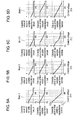
- Fig. 3 is a graph illustrating frequency characteristic of local oscillator 1, which shows the relationship between first variable capacitance control voltage (V T ) applied to control voltage input terminal 35 and oscillation frequency (f OSC ) of local oscillator 1.
- bands 1 to 4 show the characteristic of V T against fosc when on and off of first switches 411a and 411b and second switches 421a and 421b are combined in four ways.
- a bold line for each of bands 1 to 4 shows the characteristic that frequency control sensitivity of V T against fosc is substantially the same level in all bands 1 to 4.
- a dotted line for each of bands 1 to 4 shows the characteristic that frequency control sensitivity of V T against f OSC becomes higher for bands with higher f OSC in bands 1 to 4, which is the characteristic of conventional local oscillator 10.
- Fig. 4 is a graph illustrating phase noise characteristic of local oscillator 1 in Fig. 1 , which shows the relationship between oscillation frequency (f OSC ) of local oscillator 1 and phase noise.
- a bold line and dotted line in Fig. 4 show the difference between two types of frequency characteristic shown in Fig. 3 . More specifically, the bold line is the phase noise characteristic of this exemplary embodiment when frequency control sensitivity of V T against fosc is substantially the same level in all bands 1 to 4. The phase noise is substantially constant over a broad frequency range.
- the dotted line is the conventional phase noise characteristic when frequency control sensitivity of V T against fosc increases for bands with higher f OSC in bands 1 to 4. The phase noise increases as oscillation frequency becomes higher and frequency control sensitivity becomes higher.
- local oscillator 1 switches the capacity value of second variable capacitance section 430 and the capacity value of first variable capacitance section 33 relative to one another by the first control signal and second control signal output to first capacitance control terminal 413 and second capacitance control terminal 423 from frequency-adjusting circuit 670 of PLL 60.
- This achieves the setting that the capacity value of first variable capacitance section 33 changes in a small level against control voltage V T as the capacity value of second variable capacitance section 430 becomes smaller (higher oscillation frequency band).
- the characteristic shown by the dotted line in Figs. 3 and 4 can be adjusted to the characteristic shown by the bold line.
- the frequency control sensitivity can be set to substantially the same level in all bands 1 to 4, and thus the phase noise characteristic can be kept at substantially the same level over a broad frequency range.
- Figs. 5A to 5D are graphs illustrating a change in capacity value of first variable capacitance section 33 in bands 1 to 4 shown in Fig. 3 , respectively. It shows the relationship between control voltage V T applied to control voltage input terminal and the capacity value of first variable capacitance section 33. From the top row, these drawings show the capacity values of variable capacitance circuits 32a and 32b, the capacity values of first variable capacitance circuits 31a and 31b, and the capacity value of the entire first variable capacitance section 33.
- a practical use range of control voltage V T in Figs. 5A to 5D is a range between VL and VH.
- Bands 1 to 4 in Figs. 5A to 5D differ with respect to voltage setting of first reference voltage V REF1 and second reference voltage V REF2 .
- First reference voltage V REF1 and second reference voltage V REF2 set in each band are output voltages of first reference-voltage generating circuit 6 and second reference-voltage generating circuit 7 shown in Table 1.
- control voltage V T The horizontal axis in Figs. 5A to 5D is control voltage V T .
- Control voltage V T is applied to each contact point where back gates of first variable capacitive elements 310a and 310b and second variable capacitive elements 320a and 320b are connected.
- First reference voltage V PEF1 and second reference voltage V REF2 are also applied to each contact point where their gates are connected. Accordingly, each capacity value decreases as control voltage V T increases.
- Each capacity value decreases, by contraries, as first reference voltage V REF1 and second reference voltage V PEF2 increase.
- Band 1 shown in Fig. 5A , shows the state in which the capacity value of first variable capacitance section 33 changes most.
- the capacity values of first variable capacitance circuits 31a and 3b and second variable capacitance circuits 32a and 32b can be changed over the entire practical range of use (VL to VH) of control voltage V T . Accordingly, the capacitance of first variable capacitance section 33, configured by connecting in parallel first variable capacitance circuits 31a and 31b and second variable capacitance circuit 32a and 32b, can be widely varied.
- the voltages of V REF1 and V REF2 are reversed with respect to polarity for (1/6) x VCC from Band 1, respectively.
- the capacitance of first variable capacitance circuits 31a and 31b and second variable capacitance circuits 32a and 32b saturates at near VL and VH, respectively, and thus the capacitance change of first variable capacitance section 33 is smaller than that of Band 1.
- first variable capacitance section 33 can vary the relationship of capacitance change against control voltage V T by reversing the polarity of first and second reference voltages V REF1 and V REF2 .
- Formulae 10 to 12 are derived from Formulae 5 to 8 for expressing the relationship between control voltage V T of first variable capacitance section 33 and its capacitance change to be set when frequency control sensitivities of bands 1 to 4 are approximately the same.
- the relationship between control voltage VT and capacitance change is expressed by ⁇ Vt + ⁇ .
- Provision of multiple variable capacitive elements to which different reference voltages can be set enables lowering of frequency control sensitivity of the local oscillator in high oscillation frequency bands by switching these reference voltages. This achieves substantially constant frequency control sensitivity over the entire oscillation frequency range of the local oscillator. Accordingly, the phase noise characteristic can be improved over the broad frequency range.
- Fig. 1 two pairs, which are first capacitance switch circuits 41a and 41b and second capacitance switch circuits 42a and 42b, are used for second variable capacitance section 430.
- the number of pairs, values of capacitive elements 410a and 410b, and capacity values of capacitive elements 420a and 420b may be appropriately selected in accordance with a predetermined range of oscillation frequency.
- Fig. 1 refers to the structure that employs two pairs for first variable capacitance section 33: First variable capacitive elements 310a and 310b and second variable capacitive elements 320a and 320b. However, three or more pairs may also be used.
- third reference-voltage generating circuit 50 may be provided so as to output third reference voltage V REF3 from third reference voltage terminal 332 in accordance with the first control signal and the second control signal.
- This third reference voltage V REF3 and control voltage V T from control voltage input terminal 35 are applied to each terminal.
- Third variable capacitance circuits 33a and 33b connected in parallel to first variable capacitance circuits 31a and 31b and second variable capacitance circuits 32a and 32b are added.
- Third variable capacitance circuit 33a includes, same as first variable capacitance circuit 31a and second variable capacitance circuit 32a, third variable capacitive elements 330a for changing the capacity value based on control voltage V T and reference voltage V REF3 .
- capacitive element 331a connected in series to first variable capacitive element 330a is provided.
- third variable capacitive element 330b for changing the capacity value based on control voltage V T and reference voltage V REF3 is provided on third variable capacity circuit 33b, same as first variable capacitance circuit 31b and second variable capacitance circuit 32b.
- Capacitive element 331b connected in series to first variable capacitive element 330b is also provided.
- the capacitance change with respect to control voltage V T of third variable capacitive elements 330a and 330b added is controlled independently from first variable capacitive elements 310a and 310b and second variable capacitive elements 320a and 320b. Accordingly, the frequency control sensitivity of local oscillator can be even more finely adjusted. This enables improvement of the phase noise characteristic over an even broader frequency range.
- Fig. 7 shows first reference-voltage generating circuit 6 and second reference-voltage generating circuit 7 in the second exemplary embodiment.
- First reference-voltage generating circuit 6 and second reference-voltage generating circuit 7 in Fig. 7 are configured with diodes 681 to 684 and 781 to 784 in four pairs of voltage generating circuits, respectively, whose resistance-splitting ratios are different between VCC and GND. This point is different from the first exemplary embodiment.
- a diode is generally used to prevent any unnecessary increase in current consumption and any increase in circuit scale due to the need for resistors as shown in Fig. 2 .
- First reference-voltage generating circuit 6 includes four groups of voltage generating circuits in which resistances 611 to 618, switches 621 to 628, and diodes 681 to 684 are connected in series, respectively. For example, if one group of voltage generating circuits, in which resistance 612 (R1), diode 681, switch 622, switch 621, and resistance 611 (R2) are connected in series from the VCC side to GND side is selected, first reference voltage V REF1 indicated in Formula 13 is output from the point where switch 622 and switch 621 are connected.
- second reference-voltage generating circuit 7 includes four groups of voltage generating circuits in which resistances 711 to 718, switches 721 to 728, and diodes 781 to 784 are connected in series, respectively. For example, if one group of voltage generating circuits, in which resistance 712 (R1), switch 722, switch 721, diode 781, and resistance 711 (R2) are connected in series from the VCC side to GND side is selected, second reference voltage V REF2 indicated in Formula 14 is output from the point where switch 22 and switch 721 are connected.
- First variable capacitance section 33 including first variable capacitance circuits 31a and 31b and second variable capacitance circuits 32a and 32b, to which first reference voltage V REF1 and second reference voltage V REF2 are applied, show the capacity value with small temperature fluctuations. Accordingly, the temperature fluctuation of oscillation frequency output from local oscillator 1 can be reduced.
- Fig. 8 is a schematic diagram of an embodiment of electronic device of the present invention equipped with a receiver using the local oscillator in the first exemplary embodiment or the second exemplary embodiment.
- Fig. 8 shows a TV broadcast receiver as one embodiment of the electronic device.
- the TV broadcast receiver in this exemplary embodiment includes local oscillator 81 described in the first exemplary embodiment or the second exemplary embodiment.
- the TV broadcast receiver in this exemplary embodiment also includes mixer 83 for converting the incoming signal received by antenna 82 to an intermediate-frequency signal by using a local signal output from local oscillator 81.
- the TV broadcast receiver in this exemplary embodiment also includes demodulator 84 for demodulating the intermediate-frequency signal output from this mixer 83.
- the TV broadcast receiver in this exemplary embodiment further includes signal processor 85 connected to the output side of demodulator 84, and playback unit 86 including a speaker and display device connected to the output side of signal processor 85.
- Receiver 87 of the present invention is configured with local oscillator 81, mixer 83, and demodulator 84.
- high-frequency amplifier 88 is connected between antenna 82 and mixer 83, and intermediate-frequency amplifier 89 is connected between mixer 83 and demodulator 84.
- high-quality images and sound are produced by achieving a good phase noise characteristic over a broad frequency range.
- a tuner is configured with the receiver using the local oscillator described in the first exemplary embodiment or the second exemplary embodiment, broadcasts over a broad frequency range can be received, and high-quality images and sound can be produced thanks to good phase noise characteristic.
- a communications system is configured with the electronic device using the local oscillator described in the first exemplary embodiment or the second exemplary embodiment, the system is applicable to communications standards for different frequency bands, and high-quality images, sound, and data can be transmitted and received thanks to good phase noise characteristic.
- the local oscillator of the present invention achieves a broad oscillation frequency range and good phase noise characteristic at the same time, and is applicable to electronic device such as mobile terminals and TV broadcast receiver for vehicles.
- the present invention is applicable to a tuner that needs to receive broadcasts over a broad frequency range and reproduce high-quality images, sound, and data.
- the present invention is also applicable to communications systems that require supporting of communications standards with different frequency bands and the transmission and reception of high-quality images, sound, and data.
Abstract
Description
- The present invention relates to local oscillators, and receivers and electronic devices using a local oscillator.
- A conventional local oscillator disclosed in
Patent Document 1 is described with reference toFig. 9 . InFig. 9 ,conventional oscillator 10 includesoscillation circuit 2 andresonance circuit 30 connected to thisoscillation circuit 2.Oscillation circuit 2 andresonance circuit 30 are connected in a loop withPLL circuit 60. -
Resonance circuit 30 includesinductor elements oscillation circuit 2.Inductor elements Resonance circuit 30 includes firstvariable capacitance section 330 connected in parallel toinductor elements variable capacitance section 430 connected in parallel to this firstvariable capacitance section 330. Firstvariable capacitance section 330 is connected in parallel toinductor elements capacitive elements voltage input terminal 35 and reference voltage VREF supplied fromreference voltage supply 500, andcapacitive elements capacitive elements reference voltage supply 500. Variablecapacitive element 310a andcapacitive element 311a, and variablecapacitive element 310b andcapacitive element 311a are connected in series, respectively. Their contact points are connected to controlvoltage input terminal 35. Variablecapacitive element 310a andcapacitive element 311a, and variablecapacitive element 310b andcapacitive element 311b configurevariable capacitance circuits - Second
variable capacitance section 430 includes firstcapacitance switch circuits inductor elements capacitance switch circuits capacitance switch circuits capacitance switch circuit 41a includescapacitive element 410a andfirst switch 411a connected in series to thiscapacitive element 410a. Thisfirst switch 411a is switched between on and off by a signal supplied from firstcapacitance control terminal 413. In the same way, firstcapacitance switch circuit 41b includescapacitive element 410b andfirst switch 411b connected in series to thiscapacitive element 410b. Thisfirst switch 411b is switched on and off by a signal supplied from firstcapacitance control terminal 413.First switches capacitance switch circuit 42a includescapacitive element 420a andsecond switch 421a connected in series to thiscapacitive element 420a. This second switch 21a is switched between on and off by a signal supplied from secondcapacitance control terminal 423. In the same way, secondcapacitance switch circuit 42b includescapacitive element 420b andsecond switch 421b connected in series to thiscapacitive element 420b. Thissecond switch 421b is switched between on and off by a signal supplied from secondcapacitance control terminal 423.Second switches - A characteristic of oscillation frequency of
local oscillator 10 as configured above is described next with reference toFigs. 9 and10 . - In
Fig. 9 , the frequency of the oscillation signal fromlocal oscillator 10 is the resonance frequency ofresonance circuit 30. This resonance frequency is determined by firstvariable capacitance section 330, secondvariable capacitance section 430, andinductors capacitive elements variable capacitance section 330 are determined by the reference voltage supplied fromreference voltage supply 500 and the control voltage supplied from controlvoltage input terminal 35. The capacity value of secondvariable capacitance section 430 is determined by how many ofcapacitive elements capacitive elements first switches second switches - A control signal output from frequency-adjusting
circuit 670 ofPLL 600 is used for controllingfirst switches second switches circuit 670 compares the frequency difference between output signal fDIV of oscillation-frequency divider 610 and output signal fREF of reference-frequency divider 630, and determines a capacity value that minimizes the frequency difference between fDIV and FREF. Frequency-adjustingcircuit 670 then examines the combination ofcapacitive elements capacitive elements first switches second switches capacitance control terminals -
Fig. 10 is a graph illustrating frequency characteristic, which shows the relationship between first variable capacitance control voltage (VT) applied to controlvoltage input terminal 35 and oscillation frequency (fosc) oflocal oscillator 10 inFig. 9 .Bands 1 to 4 show the characteristic of VT vs. fosc whenfirst switches second switches - In
Band 1, in which fosc is the lowest,first switches second switches variable capacitance section 430 is the sum ofcapacitive elements capacitive elements Band 4, in which fosc is the highest,first switches second switches variable capacitance section 430 is approximately 0. InBands Band 1 andBand 4, only one offirst switches second switches variable capacitance section 430 becomes capacity value CSW1 ofcapacitive element capacitive element capacitive elements capacitive elements Band 2 is that onlyfirst switches Band 3 is that onlysecond switches - Oscillation frequencies fOSC1 to fOSC4 of
Bands 1 to 4 are expressed byFormulae 1 to 4.


- Frequency control sensitivity dfOSC1/dVT to dfOSC4/dVT, which are gradients of VT vs. fOSC in
bands 1 to 4 are expressed by the following formulae 5 to 8.


- Next, the relationship of frequency control sensitivity dfOSC1/dVT to dfOSC4/dVT of
bands 1 to 4, based on formulae 5 to 8, can be expressed by formula 9.
whereas, a value of each element ofresonance circuit 30 in theabove Formula 1 to Formula 9 is: - L: Inductance of
inductor elements - C1: Capacity value of
capacitive elements - CVT: Capacity value when control voltage VT is applied to the control voltage input terminals of variable
capacitive elements - CSW1 = CSW2/2: The relationship between capacity value CSW1 of
capacitive elements capacitive elements - As shown in
Fig. 10 and Formula 9, the frequency control sensitivity, which is a gradient of VT vs. fOSC ofbands 1 to 4, in this conventionallocal oscillator 10 becomes higher for a band with higher oscillation frequency fosc. In a band with high frequency control sensitivity, fosc fluctuates by voltage noise superimposed on control voltage VT, and thus a phase noise oflocal oscillator 10 degrades. - In recently-popular broadcast receiving systems and communications systems that employ digital modulation, a local oscillator with next features are demanded: A broad oscillation frequency range for handling multiple divided frequency bands, and good phase noise characteristic that does not degrade a bit-error rate even if signals are phase-modulated to multiple values for achieving high-quality image, sound, and data.
- Patent Document: Japanese Patent No.
3488180 - The present invention solves these disadvantages, and offers a local oscillator that can achieve both a broad oscillation frequency range and good phase noise characteristic.
- To achieve this object, the local oscillator of the present invention includes an oscillation circuit and a resonance circuit connected to this oscillation circuit. This resonance circuit includes an inductor element connected to the oscillation circuit, a first variable capacitance section connected to this inductor element, and a second variable capacitance section connected in parallel to this first variable capacitance section: The first variable capacitance section includes a first variable capacitive element connected to the inductor element, and a second variable capacitive element connected in parallel to this first variable capacitive element. The first variable capacitive element changes its capacity value based on control voltage and first reference voltage, and the second variable capacitive element changes its capacity value based on the control voltage and second reference voltage. In the local oscillator of the present invention, the first reference voltage and the second reference voltage are controlled based on the capacity value of the second variable capacitance section.
- With the above structure, the present invention decreases a frequency control sensitivity of the local oscillator in high oscillation-frequency bands by providing multiple variable capacitive elements to which different reference voltages can be set, and switching these reference voltages. This offers substantially constant frequency control sensitivity within the entire oscillation-frequency range of the local oscillator. Accordingly, the phase noise characteristic can be improved over the broad frequency range.
- If the local oscillator of the present invention is employed in configuring a receiver such as a tuner, or an electronic device for communications system, broadcast standards with a broad frequency range and communications standards with different frequency bands can be supported. In addition, good phase noise characteristic achieves transmission and reception of high-quality images, sound, and data.
-
-
Fig. 1 is a block diagram of a local oscillator in accordance with a first exemplary embodiment of the present invention. -
Fig. 2 is a block diagram of a first reference-voltage generating circuit and a second reference-voltage generating circuit in accordance with the first exemplary embodiment of the present invention. -
Fig. 3 is a graph illustrating frequency characteristic in accordance with the first exemplary embodiment of the present invention. -
Fig. 4 is a graph illustrating noise characteristic in accordance with the first exemplary embodiment of the present invention. -
Fig. 5A is a graph illustrating changes in a capacity value of a first variable capacitance section inband 1 in accordance with the first exemplary embodiment of the present invention. -
Fig. 5B is a graph illustrating changes in a capacity value of the first variable capacitance section inband 2 in accordance with the first exemplary embodiment of the present invention. -
Fig. 5C is a graph illustrating changes in a capacity value of the first variable capacitance section inband 3 in accordance with the first exemplary embodiment of the present invention. -
Fig. 5D is a graph illustrating changes in a capacity value of the first variable capacitance section inband 4 in accordance with the first exemplary embodiment of the present invention. -
Fig. 6 is a block diagram of another example of the first variable capacitance section in accordance with the first exemplary embodiment of the present invention. -
Fig. 7 is a block diagram of a first reference-voltage generating circuit and a second reference-voltage generating circuit in accordance with a second exemplary embodiment of the present invention. -
Fig. 8 is a schematic diagram of an electronic device in accordance with an exemplary embodiment of the present invention. -
Fig. 9 is a block diagram of a conventional local oscillator. -
Fig. 10 is a graph illustrating frequency characteristic in accordance with the conventional local oscillator. -
- 1, 81
- Local oscillator
- 2
- Oscillation circuit
- 3
- Resonance circuit
- 6
- First reference-voltage generating circuit
- 7
- Second reference-voltage generating circuit
- 11a, 11b
- Transistor
- 13a, 13b, 15a, 15b,311a,311b,321a,321b,331a,331b,410a,410b, 420a, 420b
- Capacitive element
- 17a, 17b
- Resistance
-
18a 18b - Local oscillation signal output terminal
- 19
- Constant current source
- 20a, 20b
- Inductor element
- 31a, 31b
- First variable capacitance circuit
- 32a, 32b
- Second variable capacitance circuit
- 33a, 33b
- Third variable capacitance circuit
- 33
- First variable capacitance
- 35
- Control voltage input terminal
- 41a, 41b
- First capacitance switch circuit
- 42a, 42b
- Second capacitance switch circuit
- 50
- Third reference-voltage generating circuit
- 60
- PLL
- 82
- Antenna
- 83
- Mixer
- 84
- Demodulator
- 85
- Signal processor
- 86
- Playback unit
- 87
- Receiver
- 88
- High-frequency amplifier
- 89
- Intermediate-frequency amplifier
- 310a, 310b
- First variable capacitive element
- 312
- First reference voltage terminal
- 320a, 320b
- Second variable capacitive element
- 322
- Second reference voltage terminal
- 330a, 330b
- Third variable capacitive element
- 332
- Third reference voltage terminal
- 411a, 411b
- First switch
- 413
- First capacitance control terminal
- 421a, 421b
- Second switch
- 423
- Second capacitance control terminal
- 430
- Second variable capacitance section
- 600, 700
- Decoder circuit
- 610
- Oscillation-frequency divider
- 611 to 618, 711 to 718
- Resistance
- 620
- Reference-frequency input terminal
- 621 to 628, 721 to 728
- Switch
- 630
- Reference-frequency divider
- 640
- Phase comparator
- 650
- Charge pump
- 660
- Loop filter
- 670
- Frequency-adjusting circuit
- 681 to 684, 781 to 784
- Diode
- Exemplary embodiments of the present invention are described below with reference to drawings.
- The first exemplary embodiment of the present invention is described below with reference to
Fig. 1. Fig. 1 is a block diagram of a local oscillator in this exemplary embodiment. - In
Fig. 1 ,local oscillator 1 includesoscillation circuit 2 andresonance circuit 3 connected to thisoscillation circuit 2.Oscillation circuit 2 andresonance circuit 3 are connected in a loop withPLL circuit 60. A receiver (not illustrated) employing thislocal oscillator 1 includes a mixer (not illustrated) for converting a received signal to a intermediate-frequency signal using a local signal output from local oscillationsignal output terminals local oscillator 1, and a demodulator (not illustrated) for demodulating an intermediate-frequency signal output from this mixer. An electronic device (not illustrated) employing thislocal oscillator 1 includes a signal processor connected to an output side of this demodulator, and a display unit (not illustrated) such as a liquid crystal display or a sound playback unit (not illustrated) such as a speaker. -
Resonance circuit 3 includesinductor elements oscillation circuit 2.Inductor elements Resonance circuit 3 further includes first variable capacitance section 33 and secondvariable capacitance section 430 that are connected in parallel to this first variable capacitance section 33. - First variable capacitance section 33 includes first
variable capacitance circuits variable capacitance circuits inductor elements - First
variable capacitance circuits voltage input terminal 35 and first reference voltage VREF1 supplied from first reference-voltage generating circuit 6 via firstreference voltage terminal 312. Firstvariable capacitance circuits capacitive elements capacitive elements reference voltage terminal 312. In the same way, variablecapacitive element 310b andcapacitive element 311b are connected in series, and their contact point is connected to controlvoltage input terminal 35.Capacitive elements inductor elements voltage input terminal 35 via variablecapacitive elements - Second
variable capacitance circuits voltage input terminal 35 and second reference voltage VREF2 supplied from second reference-voltage generating circuit 7 via secondreference voltage terminal 322. Secondvariable capacitance circuits capacitive elements capacitive elements reference voltage terminal 322.Variable capacitive element 320a andcapacitive element 321a, and variablecapacitive element 320b andcapacitive element 321b are connected in series, respectively. Each of their contact points is connected to controlvoltage input terminal 35.Capacitive elements inductor elements capacitive elements voltage input terminal 35. - Second
variable capacitance section 430 includes firstcapacitance switch circuits inductor elements capacitance switch circuits capacitance switch circuits capacitance switch circuit 41a includes capacitive element (third capacitive element) 410a andfirst switch 411a connected in series to thiscapacitive element 410a.First switch 411a is turned on and off by a signal supplied from firstcapacitance control terminal 413. In the same way, firstcapacitance switch circuit 41b includes capacitive element (third capacitive element) 410b andfirst switch 411b connected in series to thiscapacitive element 410b.First switch 411b is turned on and off by a signal supplied from firstcapacitance control terminal 413.First switch 411a andfirst switch 411b are connected in series, and their contact point is connected to GND. Secondcapacitance switch circuit 42a includes capacitive element (fourth capacitive element) 420a andsecond switch 421a connected in series to thiscapacitive element 420a.Second switch 421a is turned on and off by a signal supplied from secondcapacitance control terminal 423. In the same way, secondcapacitance switch circuit 42b includes capacitive element (fourth capacitive element )420b andsecond switch 421b connected in series to thiscapacitive element 420b. Second switch 421 is turned on and off by a signal supplied from secondcapacitance control terminal 423.Second switch 421a andsecond switch 421b are connected in series, and their contact point is connected to GND. -
Oscillation circuit 2 includes twoNPN transistors resonance circuit 3, two feedbackcapacitive elements capacitive elements resistances 17a and 17b, and constantcurrent source 19, as shown inFig. 1 . - One electrode (an electrode opposite to an electrode connected to VCC) of
inductor element 20a and a collector electrode oftransistor 11a are connected, and one electrode (the electrode opposite to the electrode connected to VCC) and a collector electrode oftransistor 11b are connected. - A base electrode of
transistor 11a is connected to the collector electrode oftransistor 11b viafeedback capacitive element 13a. A base electrode oftransistor 11b is connected to the collector electrode oftransistor 11a viafeedback capacitive element 13b. In other words, one electrode of feedbackcapacitive element 13a is connected to the base electrode oftransistor 11a, and the other electrode is connected to the collector electrode oftransistor 11b. In the same way, one electrode of feedbackcapacitive element 13b is connected to the base electrode oftransistor 11b, and the other electrode is connected to the collector electrode oftransistor 11a. - An emitter electrode of
transistor 11a and an emitter electrode oftransistor 11b are connected, and their contact point is connected to one terminal of constantcurrent source 19, which is the upstream side. The other terminal of this constantcurrent source 19 is connected to GND, which is the downstream side. - A base electrode of
transistor 11a is connected to constant voltage source Vb viaresistance 17a. In the same way, a base electrode oftransistor 11b is connected to constant voltage source Vb via resistance 17b. A base electrode oftransistor 11a is connected to local oscillationsignal output terminal 18a viadecoupling capacitive element 15a. In the same way, a base electrode oftransistor 11b is connected to local oscillationsignal output terminal 18b viadecoupling capacitive element 15b. -
PLL 60 includes oscillation-frequency divider 610 connected to the output side of local oscillationsignal output terminal 18a oflocal oscillator 1, and reference-frequency divider 630 connected to reference-frequency input terminal 620.PLL 60 also includesphase comparator 640 for comparing a signal from oscillation-frequency divider 610 and a reference-frequency signal from reference-frequency divider 630.PLL 60 further includescharge pump circuit 650 that receives a comparison result ofphase comparator 640 and supplies control voltage to controlvoltage input terminal 35 of local oscillator vialoop filter 660. Accordingly,PLL 60 has a function of a control circuit for supplying control voltage toresonance circuit 3 based on a frequency of local signal output fromoscillation circuit 2. - Next, oscillation frequency characteristic of
local oscillator 1 as configured above is described. - In
Fig. 1 , the resonance frequency that is output in the opposite phase from the oscillationsignal output terminals local oscillator 1 is the resonance frequency in the resonance circuit. This resonance frequency is determined by first variable capacitance section 33, secondvariable capacitance section 430, andinductors capacitive elements voltage generating circuit 6 via firstreference voltage terminal 312 and control voltage VT applied from controlvoltage input terminal 35. In the same way, the capacity values of second variablecapacitive elements voltage generating circuit 7 via secondreference voltage terminal 322 and control voltage VT applied from controlvoltage input terminal 35. The capacity value of secondvariable capacitance section 430 is determined by how many ofcapacitive elements capacitive elements first switches second switches -
First switches second switches circuit 670 ofPLL 60. This frequency-adjustingcircuit 670 determines a capacity value that minimizes the frequency difference between fDIV and fREF by comparing output signal fDIV of oscillation-frequency divider 610 and output signal fREF of reference-frequency divider 630. Frequency-adjustingcircuit 670 considers combinations ofcapacitive elements capacitive elements first switches second switches capacitance control terminals - In a locked state of
local oscillator 1 andPPL 60, control voltage VT is applied to controlvoltage input terminal 35 oflocal oscillator 1. The first capacitance control signal and the second capacitance control signal are thus input to firstcapacitance control terminal 413 and secondcapacitance control terminal 423. - Next, first reference-
voltage generating circuit 6 and second reference-voltage generating circuit 7 are described with reference toFig. 2. Fig. 2 illustrates an example of a specific structure of first reference-voltage generating circuit 6 and second reference-voltage generating circuit 7 inFig. 1 . InFig. 2 , first reference-voltage generating circuit 6 includesdecoder circuit 600,resistances 611 to 618, and switches 621 to 628. Second reference-voltage generating circuit 7 also includesdecoder 700,resistances 711 to 718, and switches 721 to 728. -
Decoder circuits capacitance control terminal 413 and on and off of second capacitance control signal that is input from secondcapacitance control terminal 423, and output a control signal, for example, that turns on only one pair out of four pairs of output. -
Resistances 611 to 618 andswitches 621 to 628 in first reference-voltage generating circuit 6 configure four pairs of voltage generating circuits in which resistance is set in different splitting ratios between VCC and GND, and VREF1 determined by one pair of resistance splitting ratio switched on bydecoder circuit 600 is output from firstreference voltage terminal 312.Resistances 711 to 718 andswitches 721 to 728 in second reference-voltage generating circuit 7 also configure four pairs of voltage generating circuit in which resistance is set in different splitting ratios between VCC and GND, and VREF1 determined by one pair of resistance splitting ratio switched on bydecoder circuit 700 is output from secondreference voltage terminal 322. - Table 1 shows an example of setting of I/O signals of first reference-
voltage generating circuit 6 and second reference-voltage generating circuit 7 inFig. 2 .[Table 1] Input Output Setting of second variable capacitance section First capacitance control signal Second capacitance control signal First reference voltage VREF1 Second reference voltage VREF2 Band Capacity value OFF OFF GND VCC 4 0 OFF ON 1/6×VCC 5/6× VCC 3 1/2×CSW1 (=C SW2) ON OFF 2/6× VCC 4/6×VCC 2 C SW1 ON ON 3/6× VCC 3/6× VCC 1 3/2×CSW1 (=C SW1+C SW2) - In Table 1, there are four pairs of combination of first capacitance control signal and second capacitance control signal for "input", and examples of voltage setting for first reference voltage VREF1 and second reference voltage VREF2 are shown in "output." The "setting of second variable capacitance" shows capacity values of second
variable capacitance section 430 inbands 1 to 4. -
Fig. 3 is a graph illustrating frequency characteristic oflocal oscillator 1, which shows the relationship between first variable capacitance control voltage (VT) applied to controlvoltage input terminal 35 and oscillation frequency (fOSC) oflocal oscillator 1. - In
Fig. 3 ,bands 1 to 4 show the characteristic of VT against fosc when on and off offirst switches second switches - A bold line for each of
bands 1 to 4 shows the characteristic that frequency control sensitivity of VT against fosc is substantially the same level in allbands 1 to 4. A dotted line for each ofbands 1 to 4 shows the characteristic that frequency control sensitivity of VT against fOSC becomes higher for bands with higher fOSC inbands 1 to 4, which is the characteristic of conventionallocal oscillator 10. -
Fig. 4 is a graph illustrating phase noise characteristic oflocal oscillator 1 inFig. 1 , which shows the relationship between oscillation frequency (fOSC) oflocal oscillator 1 and phase noise. A bold line and dotted line inFig. 4 show the difference between two types of frequency characteristic shown inFig. 3 . More specifically, the bold line is the phase noise characteristic of this exemplary embodiment when frequency control sensitivity of VT against fosc is substantially the same level in allbands 1 to 4. The phase noise is substantially constant over a broad frequency range. On the other hand, the dotted line is the conventional phase noise characteristic when frequency control sensitivity of VT against fosc increases for bands with higher fOSC inbands 1 to 4. The phase noise increases as oscillation frequency becomes higher and frequency control sensitivity becomes higher. - In this exemplary embodiment,
local oscillator 1 switches the capacity value of secondvariable capacitance section 430 and the capacity value of first variable capacitance section 33 relative to one another by the first control signal and second control signal output to firstcapacitance control terminal 413 and secondcapacitance control terminal 423 from frequency-adjustingcircuit 670 ofPLL 60. This achieves the setting that the capacity value of first variable capacitance section 33 changes in a small level against control voltage VT as the capacity value of secondvariable capacitance section 430 becomes smaller (higher oscillation frequency band). Accordingly, the characteristic shown by the dotted line inFigs. 3 and 4 can be adjusted to the characteristic shown by the bold line. In other words, the frequency control sensitivity can be set to substantially the same level in allbands 1 to 4, and thus the phase noise characteristic can be kept at substantially the same level over a broad frequency range. -
Figs. 5A to 5D are graphs illustrating a change in capacity value of first variable capacitance section 33 inbands 1 to 4 shown inFig. 3 , respectively. It shows the relationship between control voltage VT applied to control voltage input terminal and the capacity value of first variable capacitance section 33. From the top row, these drawings show the capacity values ofvariable capacitance circuits variable capacitance circuits Figs. 5A to 5D is a range between VL and VH. -
Bands 1 to 4 inFigs. 5A to 5D differ with respect to voltage setting of first reference voltage VREF1 and second reference voltage VREF2. First reference voltage VREF1 and second reference voltage VREF2 set in each band are output voltages of first reference-voltage generating circuit 6 and second reference-voltage generating circuit 7 shown in Table 1. - The horizontal axis in
Figs. 5A to 5D is control voltage VT. Control voltage VT is applied to each contact point where back gates of first variablecapacitive elements capacitive elements -
Band 1, shown inFig. 5A , shows the state in which the capacity value of first variable capacitance section 33 changes most. The voltage is set based on VPEF1 = VREF2 = (3/6) x VCC. The capacity values of firstvariable capacitance circuits 31a and 3b and secondvariable capacitance circuits variable capacitance circuits variable capacitance circuit - Next,
Band 2, shown inFig. 5B , has the voltage set based on VREP1 = (2/6) x VCC and VREF2 = (4/6) x VCC. The voltages of VREF1 and VREF2 are reversed with respect to polarity for (1/6) x VCC fromBand 1, respectively. The capacitance of firstvariable capacitance circuits variable capacitance circuits Band 1. - In the same way, in
Band 3, shown inFig. 5C , the voltages of VREF1 and VREF2 are reversed with respect to polarity for (1/6) x VCC fromBand 2, respectively. InBand 4, shown inFig. 5D , the voltages of VREF1 and VREF2 are reversed with respect to polarity for (1/6) x VCC fromBand 3. Accordingly, the capacitance change of firstvariable capacitance circuits variable capacitance circuits - In other words, as shown in
Figs. 5A to 5D , first variable capacitance section 33 can vary the relationship of capacitance change against control voltage VT by reversing the polarity of first and second reference voltages VREF1 and VREF2. -
Formulae 10 to 12 are derived from Formulae 5 to 8 for expressing the relationship between control voltage VT of first variable capacitance section 33 and its capacitance change to be set when frequency control sensitivities ofbands 1 to 4 are approximately the same. The relationship between control voltage VT and capacitance change is expressed by αVt + β. - The relationship of coefficients α1 to α4 and β1 to β4 in
bands 1 to 4 to which different first and second reference voltages VREF1 and VREF2 are applied can be set to those indicated inFormulae 10 to 12.


- Provision of multiple variable capacitive elements to which different reference voltages can be set enables lowering of frequency control sensitivity of the local oscillator in high oscillation frequency bands by switching these reference voltages. This achieves substantially constant frequency control sensitivity over the entire oscillation frequency range of the local oscillator. Accordingly, the phase noise characteristic can be improved over the broad frequency range.
- In
Fig. 1 , two pairs, which are firstcapacitance switch circuits capacitance switch circuits variable capacitance section 430. However, the number of pairs, values ofcapacitive elements capacitive elements -
Fig. 1 refers to the structure that employs two pairs for first variable capacitance section 33: First variablecapacitive elements capacitive elements - For example, as shown in
Fig. 6 , third reference-voltage generating circuit 50 may be provided so as to output third reference voltage VREF3 from thirdreference voltage terminal 332 in accordance with the first control signal and the second control signal. This third reference voltage VREF3 and control voltage VT from controlvoltage input terminal 35 are applied to each terminal. Thirdvariable capacitance circuits variable capacitance circuits variable capacitance circuits variable capacitance circuit 33a includes, same as firstvariable capacitance circuit 31a and secondvariable capacitance circuit 32a, third variablecapacitive elements 330a for changing the capacity value based on control voltage VT and reference voltage VREF3. In addition,capacitive element 331a connected in series to firstvariable capacitive element 330a is provided. In the same way, third variablecapacitive element 330b for changing the capacity value based on control voltage VT and reference voltage VREF3 is provided on thirdvariable capacity circuit 33b, same as firstvariable capacitance circuit 31b and secondvariable capacitance circuit 32b.Capacitive element 331b connected in series to firstvariable capacitive element 330b is also provided. - In this structure, the capacitance change with respect to control voltage VT of third variable
capacitive elements capacitive elements capacitive elements - The second exemplary embodiment of the present invention is described below with reference to
Fig. 7 . Components that are the same as those in the first exemplary embodiment are given the same reference marks. Only the point that differs is described.Fig. 7 shows first reference-voltage generating circuit 6 and second reference-voltage generating circuit 7 in the second exemplary embodiment. - First reference-
voltage generating circuit 6 and second reference-voltage generating circuit 7 inFig. 7 are configured withdiodes 681 to 684 and 781 to 784 in four pairs of voltage generating circuits, respectively, whose resistance-splitting ratios are different between VCC and GND. This point is different from the first exemplary embodiment. - To configure a circuit for generating a predetermined voltage in a semiconductor, a diode is generally used to prevent any unnecessary increase in current consumption and any increase in circuit scale due to the need for resistors as shown in
Fig. 2 . - First reference-
voltage generating circuit 6 includes four groups of voltage generating circuits in whichresistances 611 to 618,switches 621 to 628, anddiodes 681 to 684 are connected in series, respectively. For example, if one group of voltage generating circuits, in which resistance 612 (R1),diode 681,switch 622,switch 621, and resistance 611 (R2) are connected in series from the VCC side to GND side is selected, first reference voltage VREF1 indicated in Formula 13 is output from the point whereswitch 622 and switch 621 are connected. - In Formula 13, voltage changes in the forward direction with respect to a temperature change according to voltage VBE generated in
diode 681 between the base and emitter.

- In the same way, second reference-
voltage generating circuit 7 includes four groups of voltage generating circuits in whichresistances 711 to 718,switches 721 to 728, anddiodes 781 to 784 are connected in series, respectively. For example, if one group of voltage generating circuits, in which resistance 712 (R1),switch 722,switch 721,diode 781, and resistance 711 (R2) are connected in series from the VCC side to GND side is selected, second reference voltage VREF2 indicated in Formula 14 is output from the point where switch 22 and switch 721 are connected. - In Formula 14, voltage changes in the reverse direction with respect to a temperature change according to voltage VBE generated in
diode 781 between the base and emitter.
- In the above structure, the polarities of first reference voltage VREF1 and second reference voltage VREF2 are reversed with respect to temperature. First variable capacitance section 33 including first
variable capacitance circuits variable capacitance circuits local oscillator 1 can be reduced. -
Fig. 8 is a schematic diagram of an embodiment of electronic device of the present invention equipped with a receiver using the local oscillator in the first exemplary embodiment or the second exemplary embodiment. -
Fig. 8 shows a TV broadcast receiver as one embodiment of the electronic device. The TV broadcast receiver in this exemplary embodiment includeslocal oscillator 81 described in the first exemplary embodiment or the second exemplary embodiment. The TV broadcast receiver in this exemplary embodiment also includesmixer 83 for converting the incoming signal received byantenna 82 to an intermediate-frequency signal by using a local signal output fromlocal oscillator 81. The TV broadcast receiver in this exemplary embodiment also includesdemodulator 84 for demodulating the intermediate-frequency signal output from thismixer 83. The TV broadcast receiver in this exemplary embodiment further includessignal processor 85 connected to the output side ofdemodulator 84, andplayback unit 86 including a speaker and display device connected to the output side ofsignal processor 85. -
Receiver 87 of the present invention is configured withlocal oscillator 81,mixer 83, anddemodulator 84. - In
Fig. 8 , high-frequency amplifier 88 is connected betweenantenna 82 andmixer 83, and intermediate-frequency amplifier 89 is connected betweenmixer 83 anddemodulator 84. - In this exemplary embodiment, as described in the first and second exemplary embodiments, high-quality images and sound are produced by achieving a good phase noise characteristic over a broad frequency range.
- In the same way, if a tuner is configured with the receiver using the local oscillator described in the first exemplary embodiment or the second exemplary embodiment, broadcasts over a broad frequency range can be received, and high-quality images and sound can be produced thanks to good phase noise characteristic.
- Furthermore, if a communications system is configured with the electronic device using the local oscillator described in the first exemplary embodiment or the second exemplary embodiment, the system is applicable to communications standards for different frequency bands, and high-quality images, sound, and data can be transmitted and received thanks to good phase noise characteristic.
- The local oscillator of the present invention achieves a broad oscillation frequency range and good phase noise characteristic at the same time, and is applicable to electronic device such as mobile terminals and TV broadcast receiver for vehicles. For example, the present invention is applicable to a tuner that needs to receive broadcasts over a broad frequency range and reproduce high-quality images, sound, and data. The present invention is also applicable to communications systems that require supporting of communications standards with different frequency bands and the transmission and reception of high-quality images, sound, and data.
Claims (7)
- A local oscillator comprising:an oscillation circuit; anda resonance circuit connected to the oscillation circuit, the resonance circuit comprising:an inductor element connected to the oscillation circuit; a first variable capacitance section connected to the inductor element; and a second variable capacitance section connected in parallel to the first variable capacitance section; the first variable capacitance section comprising:a first variable capacitive element connected to the inductor element, the first variable capacitive element changing its capacity value based on a control voltage and a first reference voltage; and a second variable capacitive element connected in parallel to the first variable capacitive element, the second variable capacitive element changing its capacity value based on the control voltage and a second reference voltage;wherein,the first reference voltage and the second reference voltage are controlled based on a capacity value of the second variable capacitance section.
- The local oscillator of claim 1, the first variable capacitance section further comprising a first capacitive element connected in series to the first variable capacitive element, and a second capacitive element connected in series to the second variable capacitive element.
- The local oscillator of claim 1, wherein the second variable capacitance section comprises a third capacitive element connected in parallel to the inductor element, a first switch element connected in series to the third capacitive element, a fourth capacitive element connected in parallel to the inductor element, and a second switch element connected in series to the fourth capacitive element.
- The local oscillator of claim 1, the first variable capacitance section further comprising a third variable capacitance circuit connected in parallel to the first variable capacitance circuit, the third variable capacitance circuit changing its capacity value based on the control voltage and a third reference voltage;
wherein,
the first reference voltage, the second reference voltage, and the third reference voltage are controlled based on the capacity value of the second variable capacitance section. - The local oscillator of claim 1, comprising a first reference-voltage generating circuit for generating the first reference voltage based on the capacity value of the second variable capacitance section, and outputting the first reference voltage to the first variable capacitive element; and a second reference-voltage generating circuit for generating the second reference voltage based on the capacity value of the second variable capacitance section, and outputting the second reference voltage to the second variable capacitive element;
wherein,
polarities of the first reference voltage generated by the first reference-voltage generating circuit and the second reference voltage generated by the second reference-voltage generating circuit fluctuate in reverse directions with respect to a temperature change. - A receiver comprising:an oscillation circuit;a resonance circuit connected to the oscillation circuit, the resonance circuit comprising:an inductor element connected to the oscillation circuit; a first variable capacitance section connected to the inductor element; and a second variable capacitance section connected in parallel to the first variable capacitance section; the first variable capacitance section comprising:a first variable capacitive element connected to the inductor element, the first variable capacitive element changing its capacity value based on a control voltage and a first reference voltage; and a second variable capacitive element connected in parallel to the first variable capacitive element, the second variable capacitive element changing its capacity value based on the control voltage and a second reference voltage;a control circuit supplying the control voltage to the resonance circuit based on a frequency of a local signal output from the oscillation circuit;a mixer for converting a receiving signal to an intermediate-frequency signal using a local signal output from the oscillation circuit; anda demodulator for demodulating the intermediate-frequency signal output from the mixer;wherein,the first reference voltage and the second reference voltage are controlled based on a capacity value of the second variable capacitance section.
- An electronic device comprising:an oscillation circuit;a resonance circuit connected to the oscillation circuit, the resonance circuit comprising:an inductor element connected to the oscillation circuit; a first variable capacitance section connected to the inductor element; and a second variable capacitance section connected in parallel to the first variable capacitance section; the first variable capacitance section comprising:a first variable capacitive element connected to the inductor element, the first variable capacitive element changing its capacity value based on a control voltage and a first reference voltage; and a second variable capacitive element connected in parallel to the first variable capacitive element, the second variable capacitive element changing its capacity value based on the control voltage and a second reference voltage;a control circuit supplying the control voltage to the resonance circuit based on a frequency of a local signal output from the oscillation circuit;a mixer for converting a receiving signal to an intermediate-frequency signal using the local signal output from the oscillation circuit;a demodulator connected to an output side of the mixer;a signal processor connected to an output side of the demodulator; anda playback unit connected to an output side of the signal processor;wherein,the first reference voltage and the second reference voltage are controlled based on a capacity value of the second variable capacitance section.
Applications Claiming Priority (2)
| Application Number | Priority Date | Filing Date | Title |
|---|---|---|---|
| JP2007059450 | 2007-03-09 | ||
| PCT/JP2008/000487 WO2008123016A1 (en) | 2007-03-09 | 2008-03-07 | Local oscillator, reception device and electronic device using the same |
Publications (2)
| Publication Number | Publication Date |
|---|---|
| EP2009783A1 true EP2009783A1 (en) | 2008-12-31 |
| EP2009783A4 EP2009783A4 (en) | 2013-12-25 |
Family
ID=39830520
Family Applications (1)
| Application Number | Title | Priority Date | Filing Date |
|---|---|---|---|
| EP08720373.3A Withdrawn EP2009783A4 (en) | 2007-03-09 | 2008-03-07 | Local oscillator, reception device and electronic device using the same |
Country Status (5)
| Country | Link |
|---|---|
| US (1) | US8165550B2 (en) |
| EP (1) | EP2009783A4 (en) |
| JP (1) | JP4992903B2 (en) |
| CN (1) | CN101542895B (en) |
| WO (1) | WO2008123016A1 (en) |
Cited By (1)
| Publication number | Priority date | Publication date | Assignee | Title |
|---|---|---|---|---|
| WO2018145759A1 (en) * | 2017-02-10 | 2018-08-16 | Telefonaktiebolaget Lm Ericsson (Publ) | Electronic circuit with tuning circuit |
Families Citing this family (7)
| Publication number | Priority date | Publication date | Assignee | Title |
|---|---|---|---|---|
| JPWO2009096413A1 (en) * | 2008-01-30 | 2011-05-26 | ルネサスエレクトロニクス株式会社 | Voltage-controlled oscillator, phase-locked loop circuit, clock / data recovery circuit, and control method |
| JP5662911B2 (en) | 2011-08-31 | 2015-02-04 | ルネサスエレクトロニクス株式会社 | High frequency signal processing apparatus and radio communication system |
| US8786376B2 (en) * | 2011-12-13 | 2014-07-22 | Peraso Technologies, Inc. | Varactor voltage controlled oscillator (VCO) providing independent coarse and fine frequency tuning |
| JP6123982B2 (en) * | 2012-09-28 | 2017-05-10 | セイコーエプソン株式会社 | OSCILLATOR CIRCUIT, ELECTRONIC DEVICE, AND MOBILE BODY |
| JP6217904B2 (en) * | 2013-06-11 | 2017-10-25 | セイコーエプソン株式会社 | OSCILLATION CIRCUIT, VIBRATION DEVICE, ELECTRONIC DEVICE, MOBILE BODY, AND METHOD FOR MANUFACTURING VIBRATION DEVICE |
| CN106374836B (en) * | 2016-10-14 | 2023-07-28 | 北京无线电计量测试研究所 | Voltage-controlled temperature compensation crystal oscillator |
| CN114679197A (en) * | 2022-03-02 | 2022-06-28 | 维沃移动通信有限公司 | Radio frequency circuit, capacitance value control method thereof and electronic equipment |
Citations (3)
| Publication number | Priority date | Publication date | Assignee | Title |
|---|---|---|---|---|
| US20050134395A1 (en) * | 2003-11-24 | 2005-06-23 | Perry Colin L. | Circuit arrangement |
| US20050190002A1 (en) * | 2002-10-03 | 2005-09-01 | Koji Takinami | Voltage-controlled oscillator, radio communication apparatus and voltage-controlled oscillation method |
| US20050275478A1 (en) * | 2004-06-15 | 2005-12-15 | Takayuki Tsukizawa | Voltage controlled oscillator, and PLL circuit and wireless communication apparatus using the same |
Family Cites Families (12)
| Publication number | Priority date | Publication date | Assignee | Title |
|---|---|---|---|---|
| US5739730A (en) * | 1995-12-22 | 1998-04-14 | Microtune, Inc. | Voltage controlled oscillator band switching technique |
| JP3664006B2 (en) * | 1999-12-03 | 2005-06-22 | 松下電器産業株式会社 | Mobile communication oscillator |
| JP2001320235A (en) * | 2000-05-09 | 2001-11-16 | Matsushita Electric Ind Co Ltd | Voltage controlled oscillator |
| JP3488180B2 (en) * | 2000-05-30 | 2004-01-19 | 松下電器産業株式会社 | Frequency synthesizer |
| JP4089938B2 (en) | 2000-06-09 | 2008-05-28 | 日本電信電話株式会社 | Voltage controlled oscillator |
| JP2004056720A (en) | 2002-07-24 | 2004-02-19 | Sharp Corp | Voltage controlled oscillator, high frequency receiver using the same, and high frequency transmitter |
| JP3956795B2 (en) | 2002-08-09 | 2007-08-08 | 松下電器産業株式会社 | Voltage controlled oscillator with modulation function |
| JP2004147310A (en) * | 2002-10-03 | 2004-05-20 | Matsushita Electric Ind Co Ltd | Voltage controlled oscillator, wireless communication apparatus, and voltage controlled oscillation method |
| JP2005117428A (en) * | 2003-10-08 | 2005-04-28 | Matsushita Electric Ind Co Ltd | Voltage controlled oscillator, pll circuit, communication equipment and voltage controlled oscillating method |
| CN100594662C (en) * | 2004-02-20 | 2010-03-17 | Gct半导体公司 | LC voltage controlled oscillator with improvement of the coarse tuning time |
| US7164325B2 (en) * | 2004-03-30 | 2007-01-16 | Qualcomm Incorporated | Temperature stabilized voltage controlled oscillator |
| US7209017B2 (en) * | 2004-08-04 | 2007-04-24 | Via Technologies, Inc. | Symmetrical linear voltage controlled oscillator |
-
2008
- 2008-03-07 WO PCT/JP2008/000487 patent/WO2008123016A1/en active Application Filing
- 2008-03-07 CN CN2008800003267A patent/CN101542895B/en not_active Expired - Fee Related
- 2008-03-07 EP EP08720373.3A patent/EP2009783A4/en not_active Withdrawn
- 2008-03-07 US US12/282,080 patent/US8165550B2/en not_active Expired - Fee Related
- 2008-03-07 JP JP2008533808A patent/JP4992903B2/en not_active Expired - Fee Related
Patent Citations (3)
| Publication number | Priority date | Publication date | Assignee | Title |
|---|---|---|---|---|
| US20050190002A1 (en) * | 2002-10-03 | 2005-09-01 | Koji Takinami | Voltage-controlled oscillator, radio communication apparatus and voltage-controlled oscillation method |
| US20050134395A1 (en) * | 2003-11-24 | 2005-06-23 | Perry Colin L. | Circuit arrangement |
| US20050275478A1 (en) * | 2004-06-15 | 2005-12-15 | Takayuki Tsukizawa | Voltage controlled oscillator, and PLL circuit and wireless communication apparatus using the same |
Non-Patent Citations (1)
| Title |
|---|
| See also references of WO2008123016A1 * |
Cited By (1)
| Publication number | Priority date | Publication date | Assignee | Title |
|---|---|---|---|---|
| WO2018145759A1 (en) * | 2017-02-10 | 2018-08-16 | Telefonaktiebolaget Lm Ericsson (Publ) | Electronic circuit with tuning circuit |
Also Published As
| Publication number | Publication date |
|---|---|
| JPWO2008123016A1 (en) | 2010-07-15 |
| CN101542895B (en) | 2011-10-05 |
| CN101542895A (en) | 2009-09-23 |
| EP2009783A4 (en) | 2013-12-25 |
| WO2008123016A1 (en) | 2008-10-16 |
| US20100267352A1 (en) | 2010-10-21 |
| JP4992903B2 (en) | 2012-08-08 |
| US8165550B2 (en) | 2012-04-24 |
Similar Documents
| Publication | Publication Date | Title |
|---|---|---|
| EP2009783A1 (en) | Local oscillator, reception device and electronic device using the same | |
| US7403140B2 (en) | Receiver, digital-analog converter and tuning circuit | |
| JP5036966B2 (en) | LC oscillator with wide tuning range and low phase noise | |
| US6683509B2 (en) | Voltage controlled oscillators | |
| US5097228A (en) | Wideband oscillator with bias compensation | |
| US20090231044A1 (en) | Voltage controlled oscillator having temperature detecting circuit | |
| US20080238505A1 (en) | System and method for an automatic coarse tuning of a voltage controlled oscillator in a phase-locked loop (PLL) | |
| KR100304559B1 (en) | Selective rf circuit for double conversion tuner | |
| US7558545B2 (en) | Semiconductor device for a tuner and diversity receiver | |
| US20100093303A1 (en) | Circuit current generation apparatus and method thereof, and signal processing apparatus | |
| JP2007013898A (en) | Pll frequency synthesizer, integrated circuit and communication apparatus using the same | |
| US8270537B2 (en) | Antenna device, demodulating device and receiving device | |
| US7263336B2 (en) | Device, system and method to provide different bias voltages and common tuning voltage | |
| US7116180B2 (en) | Voltage-controlled oscillator and integrated circuit device provided with it | |
| US9281826B2 (en) | Circuit, voltage control oscillator, and oscillation frequency control system | |
| US7633561B2 (en) | Integrated circuit television receiver arrangement | |
| US7772934B2 (en) | Calibration of phase locked loop parameters based on static band information | |
| US7394329B2 (en) | Analog varactor | |
| US20090079880A1 (en) | Television Tuner | |
| US20130063661A1 (en) | Phase synchronication circuit and television signal reception circuit | |
| JP2004056720A (en) | Voltage controlled oscillator, high frequency receiver using the same, and high frequency transmitter | |
| US7355490B2 (en) | Receiver having no tracking error | |
| US7363015B2 (en) | Wide-frequency-range television tuner |
Legal Events
| Date | Code | Title | Description |
|---|---|---|---|
| PUAI | Public reference made under article 153(3) epc to a published international application that has entered the european phase |
Free format text: ORIGINAL CODE: 0009012 |
|
| 17P | Request for examination filed |
Effective date: 20080916 |
|
| AK | Designated contracting states |
Kind code of ref document: A1 Designated state(s): AT BE BG CH CY CZ DE DK EE ES FI FR GB GR HR HU IE IS IT LI LT LU LV MC MT NL NO PL PT RO SE SI SK TR |
|
| AX | Request for extension of the european patent |
Extension state: AL BA MK RS |
|
| DAX | Request for extension of the european patent (deleted) | ||
| RBV | Designated contracting states (corrected) |
Designated state(s): DE FR GB |
|
| A4 | Supplementary search report drawn up and despatched |
Effective date: 20131125 |
|
| RIC1 | Information provided on ipc code assigned before grant |
Ipc: H03L 7/18 20060101ALI20131119BHEP Ipc: H03B 5/12 20060101AFI20131119BHEP Ipc: H04B 1/26 20060101ALI20131119BHEP Ipc: H03L 7/10 20060101ALI20131119BHEP Ipc: H03L 7/099 20060101ALI20131119BHEP Ipc: H03L 7/087 20060101ALI20131119BHEP |
|
| STAA | Information on the status of an ep patent application or granted ep patent |
Free format text: STATUS: THE APPLICATION IS DEEMED TO BE WITHDRAWN |
|
| 18D | Application deemed to be withdrawn |
Effective date: 20140624 |