EP2005281B2 - Druckempfindlicher induktiver detektor zur verwendung in benutzeroberflächen - Google Patents
Druckempfindlicher induktiver detektor zur verwendung in benutzeroberflächen Download PDFInfo
- Publication number
- EP2005281B2 EP2005281B2 EP07733334.2A EP07733334A EP2005281B2 EP 2005281 B2 EP2005281 B2 EP 2005281B2 EP 07733334 A EP07733334 A EP 07733334A EP 2005281 B2 EP2005281 B2 EP 2005281B2
- Authority
- EP
- European Patent Office
- Prior art keywords
- detector
- inductive component
- inductive
- panel
- resilient panel
- Prior art date
- Legal status (The legal status is an assumption and is not a legal conclusion. Google has not performed a legal analysis and makes no representation as to the accuracy of the status listed.)
- Not-in-force
Links
Images


Classifications
-
- H—ELECTRICITY
- H03—ELECTRONIC CIRCUITRY
- H03K—PULSE TECHNIQUE
- H03K17/00—Electronic switching or gating, i.e. not by contact-making and –breaking
- H03K17/94—Electronic switching or gating, i.e. not by contact-making and –breaking characterised by the way in which the control signals are generated
- H03K17/965—Switches controlled by moving an element forming part of the switch
- H03K17/97—Switches controlled by moving an element forming part of the switch using a magnetic movable element
-
- G—PHYSICS
- G06—COMPUTING OR CALCULATING; COUNTING
- G06F—ELECTRIC DIGITAL DATA PROCESSING
- G06F3/00—Input arrangements for transferring data to be processed into a form capable of being handled by the computer; Output arrangements for transferring data from processing unit to output unit, e.g. interface arrangements
- G06F3/01—Input arrangements or combined input and output arrangements for interaction between user and computer
- G06F3/03—Arrangements for converting the position or the displacement of a member into a coded form
- G06F3/033—Pointing devices displaced or positioned by the user, e.g. mice, trackballs, pens or joysticks; Accessories therefor
- G06F3/0354—Pointing devices displaced or positioned by the user, e.g. mice, trackballs, pens or joysticks; Accessories therefor with detection of two-dimensional [2D] relative movements between the device, or an operating part thereof, and a plane or surface, e.g. 2D mice, trackballs, pens or pucks
- G06F3/03547—Touch pads, in which fingers can move on a surface
-
- G—PHYSICS
- G06—COMPUTING OR CALCULATING; COUNTING
- G06F—ELECTRIC DIGITAL DATA PROCESSING
- G06F3/00—Input arrangements for transferring data to be processed into a form capable of being handled by the computer; Output arrangements for transferring data from processing unit to output unit, e.g. interface arrangements
- G06F3/01—Input arrangements or combined input and output arrangements for interaction between user and computer
- G06F3/03—Arrangements for converting the position or the displacement of a member into a coded form
- G06F3/041—Digitisers, e.g. for touch screens or touch pads, characterised by the transducing means
- G06F3/046—Digitisers, e.g. for touch screens or touch pads, characterised by the transducing means by electromagnetic means
-
- H—ELECTRICITY
- H03—ELECTRONIC CIRCUITRY
- H03K—PULSE TECHNIQUE
- H03K17/00—Electronic switching or gating, i.e. not by contact-making and –breaking
- H03K17/94—Electronic switching or gating, i.e. not by contact-making and –breaking characterised by the way in which the control signals are generated
- H03K17/96—Touch switches
-
- H—ELECTRICITY
- H03—ELECTRONIC CIRCUITRY
- H03K—PULSE TECHNIQUE
- H03K2217/00—Indexing scheme related to electronic switching or gating, i.e. not by contact-making or -breaking covered by H03K17/00
- H03K2217/94—Indexing scheme related to electronic switching or gating, i.e. not by contact-making or -breaking covered by H03K17/00 characterised by the way in which the control signal is generated
- H03K2217/96—Touch switches
- H03K2217/96038—Inductive touch switches
Definitions
- This invention relates to a pressure sensitive detector and, in particular to such a detector for use in user interfaces.
- Push buttons typically detect a user's input by making or breaking electrical contacts. Such buttons are unreliable in harsh environments where foreign matter, fluid or impact can cause electrical contacts to fail. Protective gaiters or seals are notoriously unreliable.
- Capacitive detectors suffer from temperature or humidity drift and are often unable to differentiate between a user's finger and a water droplet, for example.
- Infra-red touch sensors are expensive and need a transparent panel such as glass between the sensor and the user.
- Piezo sensors need expensive materials and precision assembly.
- Inductive displacement detectors such as that described by the present inventors in WO 2006/064234 , have also been used but typically these require a relatively large displacement for effective touch sensing.
- WO 2004/061759 describes an apparatus to detect the position of deformation along an axis transverse to the axis of deformation. The construction is complex and is therefore relatively expensive to manufacture.
- WO 2006/064234A1 describes a device for measuring the position of a first body relative to a second body.
- WO 2006/064245 A2 describes an inductive detector for measuring the displacement of one body relative to a second.
- the present invention provides a pressure sensitive detector for a user interface comprising a first generally laminar inductive component, a second generally laminar inductive component and a resilient panel.
- the first inductive component and the second inductive component are arranged in facing relation and are mutually spaced.
- the resilient panel is arranged for flexural movement relative to the second inductive component and the first inductive component is arranged for movement with the resilient panel, whereby, in use, pressure applied to the resilient panel causes movement of the first inductive component relative to the second inductive component, and a consequent change in the inductive coupling between the first and second inductive components.
- the resilient panel has a stiffness of at least 500 N/m and the ratio of the mutually overlapping area of the first and second inductive components to the square of the spacing of the first and second inductive components is greater than 150 to 1.
- a pressure sensitive detector that has an elastically deformable resilient panel that is relatively stiff.
- the resilient panel is sufficiently robust that it can form an outer, environmentally-exposed surface of the detector, such as the keypad of a touch-sensitive input device.
- the resilient panel is relatively stiff, there is relatively little movement of the panel in response to, for example, a user's touch, and this makes the panel difficult to use as a touch-sensitive keypad.
- the invention solves this problem by providing first and second inductive components that have a very large overlapping area relative to their mutual spacing. In this way, even very small movements of the resilient panel can be detected.
- the combination of the stiff panel and the large ratio of area to spacing of the inductive components provides a very effective pressure-sensitive detector, of particular use as a user-input device.
- This invention at least in its preferred embodiments, provides a simple, robust and inexpensive apparatus to detect deformation of the resilient panel.
- the invention is particularly useful for user interfaces which often need robust panels for reliable operation in harsh environments, easy cleaning or good aesthetics, but also sensitive detection of user input.
- the first and second inductive components may be any suitable inductive components that are capable of detecting movement of the resilient panel.
- one of the first and second inductive components may be a transmit antenna and the other may be a receive antenna, with the amplitude of an AC signal received by the receive antenna being indicative of the relative spacing of the antennae.
- the first and second inductive components may take the form of one or more transmit and receive antennae.
- one of the first and second inductive components is a bulk conductor.
- the other of the inductive components is an inductor coil.
- the proximity of the bulk conductor to the inductor coil changes the inductance of the inductor coil, whereby to indicate the mutual spacing of the bulk conductor and inductor coil.
- a material of high magnetic permeability may be used as an alternative to a bulk conductor.
- the first inductive component may be a bulk conductor.
- the second inductive component may be an inductor coil.
- the first inductive component which is typically nearest to the exterior of the detector, is a passive component that does not require an electrical power connection. This simplifies the construction of the detector.
- the bulk conductor is typically composed of metal, for example copper or silver.
- the bulk conductor may be a conductive layer, for example a metal sheet or layer.
- the first inductive component may be formed by the resilient panel, which also simplifies the construction of the detector.
- the first inductive component may be mounted to the resilient panel.
- the first inductive component may be formed as a layer on the resilient panel.
- the first inductive component may be mounted directly or indirectly on the resilient panel.
- an intervening layer, such as an insulating layer, or member may be provided between the resilient panel and the first inductive component.
- the second inductive component may be formed as a layer deposited, for example printed, on a substrate, such as a printed circuit board.
- the resilient panel may be mounted (directly or indirectly) to the substrate.
- the detector may be constructed as a series of layers forming the substrate, second inductive component, first inductive component and/orthe resilient panel. This provides a particularly advantageous construction method, because of the relative simplicity of manufacturing.
- the layers of the detector such as the resilient panel, the first and second inductive components and/ or the substrate are flat (or planar).
- these layers may not be flat and may take, for example, an undulating or arcuate form.
- a spacer layer may be provided between the first and second inductive components.
- the space layer may be formed of a material having a lower Young's modulus than the resilient layer.
- the spacer layer can act to provide additional resilience to the outersurface of the detector.
- the spacer layer may act to insulate electrically the first inductive component from the second inductive component to prevent short circuits.
- the spacer layer has apertures formed therethrough which define a sensitive region of the detector.
- the resilient layer is unsupported by the space layer and can deform elastically. Outside of the apertures, the spacer layersupports the resilient layer and prevents deformation.
- the spacer layer acts to isolate mechanically the sensitive region(s) of the detector.
- the spacer layer may be formed of a rigid material, such as printed circuit board substrate material.
- the stiffness of the resilient layer is typically greater than 3,000 N/m and may be greater than 5,000 N/m. In embodiments of the invention, the stiffness of the resilient layer is greater than 30,000 N/m, particularly greater than 50,000 N/m, more particularly greater than 300,000 N/m, even more particularly greater than 500,000 N/m.
- the stiffness of the resilient layer is defined as the ratio of the force applied to the resilient layer at a given point to the deflection of the resilient layer at that point in response to the force.
- the stiffness may be determined at the point of maximum deflection of the resilient layer in the region of sensitivity of the detector.
- the Young's modulus of the resilient layer is typically greater than 2 GPa and may be greater than 5 GPa. In embodiments of the invention, the Young's modulus of the resilient layer is greater than 10 GPa, particularly greater than 20 GPa, more particularly greaterthan 40 GPa, even more particularly greaterthan 80 GPa and may be greater than 160 GPa. Similarly, the Young's modulus of the resilient layer is generally less than 500 GPa, particularly less than 300 GPa. Suitable materials for the resilient layer include stainless steel and aluminium.
- the ratio of the mutually overlapping area of the first and second inductive components to the square of the spacing of the first and second inductive components may be greater than 300 to 1, particularly greaterthan 1,000 to 1, and even greater than 3,000 to 1.
- the area occupied by the inductive component is considered as the area defined by the outermost extent of the component, rather than the surface area of component per se.
- the invention provides an apparatus to measure deformation comprising at least two laminar elements separated by a relatively small distance. At least one of the laminar elements is an inductive winding and deformation causes relative movement between at least parts of the two laminar elements.
- the invention extends to a touch sensitive user input device comprising a detector according to the invention.
- the input device may comprise a plurality of detectors.
- the detectors may have a common resilient panel.
- the input device may comprise a display device mounted to a surface of the resilient panel remote from the second inductive component.
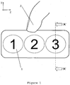
- Figure 1 shows a plan view of a device according to a first embodiment of the invention, in the form of a user interface comprising a push button keypad.
- a substantially impermeable, robust, protective fascia panel 1 made from stainless steel is printed (or etched) with user graphics.
- the panel 1 protects the keypad's interior from the environment for reasons of safety, hygiene and reliability.
- the panel 1 deforms elastically by a small amount when pushed by the user and returns to its original state afterwards.
- the detector is located behind the push button but is not shown for clarity.
- the panel 1 can be made from a range of materials which are preferably durable and strong but with some elastic properties.
- Examples of preferred materials are steel, Acrylonitrile Butadiene Styrene (ABS) mouldings, copper, aluminium, wood, glass fibre, printed circuit board PCB substrates etc.
- conductive materials also shield against electromagnetic emissions.
- the materials have a Young's Modulus of less than 270GPa (measured at room temperature).
- very hard materials such as ceramic, diamond, tungsten carbide are not used because the deformation caused by a user would be very small.
- Figure 2 shows a section along line A-A of Figure 1 in which a laminar conductive target 3 such as an electroplated copper disk is attached to the underside of the panel 1.
- the target 3 is a highly conductive material such as copper or aluminium.
- Deformation of the panel 1 causes some of the target 3 to move towards the AC energized inductors 4 and so alter its inductance. In this example the deformation causes movement towards the inductor 4 but in other arrangements deformation could cause movement away.
- the inductance value of the inductor 4 therefore changes according to deformation.
- the inductor 4 is formed as a spiral track on the upper layer of a 2-layer printed circuit board (PCB) 5.
- PCB 2-layer printed circuit board
- the PCB substrate 5 carries the inductor 4 tracks and acts as a mechanical barrier to prevent large, plastic deformation or damage.
- This barrier may be strengthened by using thick, sturdy PCB 5, additional mechanical restraints or back filling with epoxy, expanded foam etc. Such constructions are advantageous in instances where the detector must withstand impact. Shorting of the inductor tracks 4 caused by gross deformation of the target 3 can be prevented by a thin layer of insulation over the inductor 4.
- the spacer 13 is a sheet with holes to allow deformation. The spacer helps mechanically isolate each push button from its neighbours so that misreads are avoided.
- Figure 3 shows the inductor's rate of change of inductance with respect to distance moved by a target 3 in the x-axis (d ⁇ L/dX) versus position of the target3 along the x-axis (X). Note the greater rate of change or sensitivityclose to the inductor 4.
- Traditional inductive detector arrangements often aim to maximize the measurement range and miss the opportunity presented by the sensitivity very close to the inductor's windings 4. This is important in detecting very small deformations caused by light finger pressure on a stiff panel 1.
- the overlapping area of the target 3 and inductor 4 should be at least 150 units 2 and preferably >1000 units 2 .
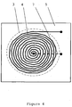
- Figure 4 shows a plan view of an inductor 4 on a 2-layer PCB co-operating with a target 3 (shown in outline) above it.
- the inductor 4 is formed as a spiral winding substantially on one PCB layer 5.
- the inductor circuit 4 is completed by taking the innermost track out using a plated via hole and a link 7.
- the link 7 is formed by a conductive track on the underside of the board.
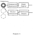
- FIG. 5 shows a simplified electronic circuit schematic.
- the circuit includes a power supply, frequency generator, inductors 4, microprocessor and an electrical output.
- the power supply is typically 5VDC, 10 milliamps for 100% duty cycle.
- the frequency generator comprises an oscillator to generate signals from 100 kHz to 10MHz, but preferably 1 to 5 MHz.
- There are various techniques which can measure inductance including an inductance bridge, current measurement or tank circuit frequency shift.
- the inductance value is compared to another inductor so that a change in inductance ratio is measured.
- the reference inductor may be the inductor 4 of one or more of the other push buttons.
- the microcontroller preferably has a flash memory with analogue inputs and is programmed to suit the application.
- the microcontroller may be dedicated to the detector system but may also carry out other functions such as display or motor control.
- Figure 3 shows an electrical output to the host system.
- a serial data stream is used but an analogue output such as 0 to 5V or 4 to 20 mA could be used.
- the electronic circuit may be augmented with a speaker to provide feedback when input is sensed. Audio feedback whelps compensate for the lack of tactile feedback but has the advantage of being programmable to a desired tone, volume etc.
- the electronics circuit will often control multiple inputs. This may be achieved by adding one or more multiplexers which can simply step through each detector in turn or use more sophisticated algorithms based on most frequently or most recently used detectors.
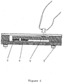
- FIG. 6 shows a sectional view of an arrangement used to amplify the small deformations in a stiff panel 1 using a lever 8.
- the lever 8 is preferably made from a cantilever or tongue of PCB material which touches the rear face of the panel 1.
- a target 3 such as a copper disk is attached to the lever 8.
- the lever 8 extends from behind the push button area.
- a bump 9 on the cantilever touches the back of the panel 1 where the user is most likely to touch.
- Other mechanical means include, for example, a disk which forms a dish shape when it is pressed close to its middle.
- Such patterns can be used to optimize the deformation produced by a given finger pressure whilst still leaving areas of thicker material (to prevent mechanical damage) when the panel is pressed hard.
- Such mechanical patterns may also be made by plastic injection moulding or machining methods.
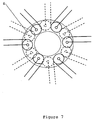
- Figure 7 shows detectors arranged in an annulus according to a second embodiment of the invention in the form of an extended touch detector where the user might apply force at a point along a straight line, curved line or circle.
- annular arrangements have been used in portable music players.
- Maximum deformation occurs where the user applies force along the circle.
- the deformation may extend over several detectors. Comparison of the readings from each of the detectors can be used to calculate the position of the applied force. In such constructions it is advantageous to break a continuous target 3 into several individual targets 3 to provide greater differentiation between neighbouring detectors.
- An alternative embodiment of the invention is a joystick.
- a joystick is attached to the panel 1 so that the user's interaction with the joystick (including upward motion) causes deformation of the panel. The interaction can be sensed by comparing the readings from multiple detectors arranged at various points on the panel.
- a further embodiment of the invention is a touch screen with detectors arranged around its edges. Inputs from multiple detectors are used to determine user input on the screen. For example, four detectors may be located under each corner of a screen held in a resilient bezel. The position of a finger at various points of the screen can be calculated by comparing the readings of the four detectors. This may be carried out initially using a teach mode and then capturing the data in electronic memory as a look up table.
- Figure 8 shows a sectional view of a yet further embodiment of the invention in the form of a touch screen or pad.
- the user causes deformation of a laminar target 3 behind a display 10 and the position of the user's input is detected by comparing the readings from a 2-dimensional pattern of detectors.
- the detectors may be arranged on multiple layers of the circuit board and overlap.
- the target 3 may be a continuous sheet or a multiplicity of targets 3 in a 2-D pattern.
- the performance of the detectors is substantially independent of the chemical composition of the screen and what is going on electrically on the screen. This is advantageous with organic light emitting and plastic electronic type displays since both the display and detector array can be produced by printing.
- An embodiment of the invention can be used to measure displacement over a larger distance by arranging a spring 11 between the panel 1 and a body 12 moving by a large distance.
- Figure 9 shows a sectional view of such an arrangement.
- the spring 11 may be arranged so that when it is far away it will pull the panel rather than push.
- Such arrangements are useful to measure the displacement of pistons in cylinders, shock absorbers and air or fluid dampers.
- inductive elements which may be used for the inductive detector using various permutations and combinations of coils, windings, targets, electrical intermediates, resonant targets etc.
- the target 3 described so far could be replaced by a shorted passive circuit or an AC energized winding.
- Arrangements may operate using changes in mutual inductance or self inductance relative to deformation.
- the deformation is into a gas cavity at atmospheric pressure.
- the cavity may be filled by a pressurised gas, liquid or highly elastic material such as rubber. These fillings can be used to prevent gross deformation and provide a restorative force after deformation.
- Elastic sheets are particularly useful in 2D arrangements.
- Electrical connections to the detector can be carried across a transformer coupling.
- Such arrangements allow the detector to be placed on a body which moves relative to the electronics controls.
- Such an arrangement might be used, for example, to measure the force applied by a rider to each pedal of a bicycle for training purposes.
- the electronic controls are positioned on the bicycle frame; the detectors are arranged to measure the force or torque applied to each pedal by the rider and the electrical supply is carried across a transformer link at the pedal crank.
- the PCB 5 containing the inductance 4 may also carry other electronic elements such as light emitting diodes (LED's) or displays.
- LED's light emitting diodes
- the invention has particular utility with printed electroluminescent (EL) inks co-operating with conductive inks.
- EL devices which would traditionally utilise membrane switches.
- each detector need not be individually connected. Instead, where inductance changes are sufficiently large, inductance change across the rows and columns of an array of detectors may be used.
- a push button 1 the characteristics of a single user input may be taught e.g. time to press down, time to return etc. The characteristics of a person keeping a finger in place can also be taught. Further, the amount of force may also be input to the host system to increase or decrease the rate at which a control parameter is altered.
- the inductor 4 may be produced with a centre tapping point so that measurements can be taken across the whole inductor or just the inner or outer portions of the inductor. Such inner or outer portions can be used as the reference inductor for ratiometric measurements.
- a stylus, pen, key or other implement could also cause deformation.
- the user might also apply a force using any part of his body.
- the electronics circuit is located close to the inductors 4 to avoid any electromagnetic compatibility (EMC) problems. If the circuit is more than a few centimetres distant, then a small loop area arrangement of conductors between the circuit and the detector should be used to avoid EMC problems. This can be achieved using twisted pair cable; arranging tracks on various layers of the PCB 5 or locating tracks on the inner layers of the PCB 5 whose outer layers are copper planes.
- EMC electromagnetic compatibility
- panel materials should not be too stiff it has been found that fairly stiff materials such as glass can be used as long as they are used as thin laminates. For example, 0.3 mm glass works well with 25mm pitch keys. To produce greater deformation, the panel 1 need not be attached on all its sides.
- a separate conductive element 3 is not needed if the panel 1 is sufficiently conductive that it can act as a combined panel 1 and target 3. Copper or silver are particularly advantageous in applicationswhere hygiene is important since userinterface panels 1 made with these materials have superior antibacterial or anti-microbial properties.
- Inductors 4 can be constructed in various ways including windings on multiple layers of a PCB; pancake style windings; printed conductive ink; single layer PCB with insulated jumpers taking the innermost winding to the outside etc.
- the detector can be arrangedto measure rotary position by measuring the deformation caused by a threaded part as it rotates in a threaded housing.
- the detector can be arranged as a combined detector and switch when the deformation also causes electrical contacts to open or close. Such contacts can be combined with the detector's laminar winding and may, for example, signal maximum deflection.
- Measuring the resistance of the inductors may be used to measure temperature.
- the detector may also be used to measure a range of parameters including pressure, weight, vibration, flow etc.
- the detector has particular utility in flow measurement since the target 3 can be arranged as a membrane with fluid on both sides to allow accurate measurement of small differential pressures and hence flow.
- Applications for the invention include but are not limited to push buttons, rocker buttons, position sensors, touch sensors, pinch sensors, impact sensors, 1 -dimensional user inputs, 2-dimensional user inputs, multi-dimensional user inputs, accelerometers, joysticks, infant/cot monitors, touch screens, touch pads, linear displacement sensors, rotary displacement sensors, weight sensors, strain sensors, vibration sensors, level sensors, impact sensors, actuator sensors, pressure sensors, differential pressure sensors, proximity sensors, torque sensors and flow sensors.
- an apparatus for user interfaces to measure inductively the deformation of a body 1 comprises at least two laminar conductive elements 3, 4, at least one of which is an AC energized inductor 4, wherein deformation causes relative axial movement between the at least two laminar elements 3, 4 and the maximum deformation distance is limited to prevent damage.
Landscapes
- Engineering & Computer Science (AREA)
- General Engineering & Computer Science (AREA)
- Theoretical Computer Science (AREA)
- Physics & Mathematics (AREA)
- Human Computer Interaction (AREA)
- General Physics & Mathematics (AREA)
- Electromagnetism (AREA)
- Measurement Of Length, Angles, Or The Like Using Electric Or Magnetic Means (AREA)
Claims (11)
- Drucksensordetektor für eine Benutzerschnittstelle, umfassend:eine erste, im Allgemeinen schichtartige induktive Komponente;eine zweite, im Allgemeinen schichtartige induktive Komponente; undein elastisches Paneel (1),wobei die erste induktive Komponente und die zweite induktive Komponente sich einander gegenüberstehend angeordnet sind und einen Abstand zwischen sich aufweisen;wobei das elastische Paneel (1) so angeordnet ist, dass es sich in Bezug auf die zweite induktive Komponente durch Biegung bewegen kann, und die erste induktive Komponente so angeordnet ist, dass sie sich mit dem elastischen Paneel (1) bewegt,wodurch bei der Anwendung ein auf das elastische Paneel (1) ausgeübter Druck bewirkt, dass sich die erste induktive Komponente in Bezug auf die zweite induktive Komponente bewegt und es infolgedessen zu einer Änderung der induktiven Kopplung zwischen der ersten und der zweiten induktiven Komponente kommt, unddadurch gekennzeichnet, dass das elastische Paneel (1) eine Steifheit von mindestens 500 N/m hat und das Verhältnis des sich gegenseitig überlappenden Bereichs der ersten und der zweiten induktiven Komponente zum Quadrat des Abstands zwischen der ersten und der zweiten induktiven Komponente größer als 150 zu 1 ist; und der Detektor eine Abstandsschicht (13) mit einer Öffnung umfasst, die eine empfindliche Region des Detektors definiert; wobei die Abstandsschicht die elastische Schicht außerhalb der Öffnung abstützt, um die empfindliche Region des Detektors mechanisch zu isolieren.
- Detektor gemäß Anspruch 1, wobei eine der ersten und der zweiten induktiven Komponente ein Volumenleiter (3) und die jeweils andere induktive Komponenten eine Induktorspule (4) ist.
- Detektor gemäß Anspruch 2, wobei die erste induktive Komponente ein Volumenleiter (3) und die zweite induktive Komponenten eine Induktorspule (4) ist.
- Detektor gemäß Anspruch 3, wobei die erste induktive Komponente durch das elastische Paneel (1) gebildet wird.
- Detektor gemäß einem der Ansprüche 1 bis 3, wobei die erste induktive Komponente an dem elastischen Paneel (1) befestigt ist.
- Detektor gemäß einem der vorherigen Ansprüche, wobei die zweite induktive Komponente als eine Schicht gebildet wird, die auf einem Substrat (5) aufgetragen ist.
- Detektor gemäß Anspruch 6, wobei das elastische Paneel (1) an dem Substrat (5) befestigt ist.
- Detektor gemäß einem der vorherigen Ansprüche, wobei durch die Abstandsschicht (13) hindurch Öffnungen ausgebildet sind, die empfindliche Regionen der Vorrichtung definieren.
- Berührungsempfindliche Eingabevorrichtung, die einen Detektor gemäß einem der vorherigen Ansprüche umfasst.
- Eingabevorrichtung gemäß Anspruch 9, umfassend eine Mehrzahl von Detektoren gemäß einem der Ansprüche 1 bis 9, wobei die Detektoren ein gemeinsames elastisches Paneel (1) haben.
- Eingabevorrichtung gemäß Anspruch 9 oder 10, umfassend eine Anzeigeeinrichtung, die entfernt von der zweiten induktiven Komponente an einer Oberfläche des elastischen Paneels (1) befestigt ist.
Priority Applications (1)
| Application Number | Priority Date | Filing Date | Title |
|---|---|---|---|
| EP08168317.9A EP2028586B3 (de) | 2006-07-22 | 2007-06-22 | Druckempfindlicher induktiver Sensor zur Verwendung in Benutzeroberflächen |
Applications Claiming Priority (12)
| Application Number | Priority Date | Filing Date | Title |
|---|---|---|---|
| GB0614631A GB0614631D0 (en) | 2006-07-22 | 2006-07-22 | Detector |
| GB0617884A GB0617884D0 (en) | 2006-07-22 | 2006-09-12 | Detector |
| GB0624366A GB0624366D0 (en) | 2006-09-12 | 2006-12-06 | Monitoring System |
| GB0700789A GB0700789D0 (en) | 2006-09-12 | 2007-01-16 | Detector |
| GB0701868A GB0701868D0 (en) | 2006-09-12 | 2007-02-01 | Detector |
| GB0702208A GB0702208D0 (en) | 2006-09-12 | 2007-02-06 | Detector |
| GB0703149A GB0703149D0 (en) | 2007-02-17 | 2007-02-17 | Touch VII |
| GB0703441A GB0703441D0 (en) | 2006-09-12 | 2007-02-22 | Touch VII |
| GB0704166A GB0704166D0 (en) | 2006-07-22 | 2007-03-02 | Detector |
| GB0704349A GB0704349D0 (en) | 2006-07-22 | 2007-03-07 | Detector |
| GB0707460A GB0707460D0 (en) | 2006-09-12 | 2007-04-17 | Detector |
| PCT/GB2007/002339 WO2008012491A1 (en) | 2006-07-22 | 2007-06-22 | Pressure sensitive inductive detector for use in user interfaces |
Related Child Applications (2)
| Application Number | Title | Priority Date | Filing Date |
|---|---|---|---|
| EP08168317.9A Division-Into EP2028586B3 (de) | 2006-07-22 | 2007-06-22 | Druckempfindlicher induktiver Sensor zur Verwendung in Benutzeroberflächen |
| EP08168317.9A Division EP2028586B3 (de) | 2006-07-22 | 2007-06-22 | Druckempfindlicher induktiver Sensor zur Verwendung in Benutzeroberflächen |
Publications (4)
| Publication Number | Publication Date |
|---|---|
| EP2005281A1 EP2005281A1 (de) | 2008-12-24 |
| EP2005281B1 EP2005281B1 (de) | 2009-08-12 |
| EP2005281B2 true EP2005281B2 (de) | 2016-04-27 |
| EP2005281B3 EP2005281B3 (de) | 2017-11-08 |
Family
ID=38565477
Family Applications (2)
| Application Number | Title | Priority Date | Filing Date |
|---|---|---|---|
| EP07733334.2A Not-in-force EP2005281B3 (de) | 2006-07-22 | 2007-06-22 | Druckempfindlicher induktiver detektor zur verwendung in benutzeroberflächen |
| EP08168317.9A Ceased EP2028586B3 (de) | 2006-07-22 | 2007-06-22 | Druckempfindlicher induktiver Sensor zur Verwendung in Benutzeroberflächen |
Family Applications After (1)
| Application Number | Title | Priority Date | Filing Date |
|---|---|---|---|
| EP08168317.9A Ceased EP2028586B3 (de) | 2006-07-22 | 2007-06-22 | Druckempfindlicher induktiver Sensor zur Verwendung in Benutzeroberflächen |
Country Status (2)
| Country | Link |
|---|---|
| EP (2) | EP2005281B3 (de) |
| WO (1) | WO2008012491A1 (de) |
Families Citing this family (18)
| Publication number | Priority date | Publication date | Assignee | Title |
|---|---|---|---|---|
| US8174372B2 (en) * | 2008-06-26 | 2012-05-08 | Immersion Corporation | Providing haptic feedback on a touch surface |
| US8858003B2 (en) | 2008-10-27 | 2014-10-14 | Microchip Technology Incorporated | Physical force capacitive touch sensors having conductive plane and backlighting |
| US8408723B2 (en) * | 2009-09-01 | 2013-04-02 | Microchip Technology Incorporated | Backlighting inductive touch buttons |
| US9116569B2 (en) | 2008-11-26 | 2015-08-25 | Blackberry Limited | Touch-sensitive display method and apparatus |
| US8810523B2 (en) * | 2009-04-20 | 2014-08-19 | Broadcom Corporation | Inductive touch screen and methods for use therewith |
| US8339372B2 (en) * | 2009-04-20 | 2012-12-25 | Broadcom Corporation | Inductive touch screen with integrated antenna for use in a communication device and methods for use therewith |
| US9543948B2 (en) * | 2009-09-01 | 2017-01-10 | Microchip Technology Incorporated | Physical force capacitive touch sensors |
| GB2489957A (en) * | 2011-04-12 | 2012-10-17 | Manu Mehra | An easily-cleaned light switch with anti-microbial properties for use in hospitals |
| US9417754B2 (en) | 2011-08-05 | 2016-08-16 | P4tents1, LLC | User interface system, method, and computer program product |
| DE102012211416A1 (de) * | 2012-07-02 | 2014-01-23 | Robert Bosch Gmbh | Wirbelstromsensor und Verfahren zum Messen einer Kraft |
| CN104995840B (zh) * | 2013-01-17 | 2019-05-21 | 密克罗奇普技术公司 | 物理力电容式触摸传感器 |
| CN103207031B (zh) * | 2013-03-19 | 2014-12-03 | 浙江大学 | 一种非接触式的温度测量装置及其测温方法 |
| ITMI20131877A1 (it) | 2013-11-12 | 2015-05-13 | Whirlpool Co | Interfaccia di comando di tipo capacitivo, in particolare per elettrodomestico, con sicurezza d'uso perfezionata |
| US9228907B2 (en) | 2013-11-14 | 2016-01-05 | Nokia Technologies Oy | Flexible device deformation measurement |
| EP3111180A1 (de) | 2014-02-26 | 2017-01-04 | 3M Innovative Properties Company | Auf kraft reagierende induktoren für kraftsensoren |
| CN112735889B (zh) | 2019-10-28 | 2024-05-24 | 北京小米移动软件有限公司 | 按键结构、电子设备及控制方法 |
| US11822035B2 (en) * | 2021-07-22 | 2023-11-21 | Ge Aviation Systems Llc | Passive inductive proximity sensor array signal processing circuit |
| KR20250141385A (ko) * | 2024-03-20 | 2025-09-29 | 삼성전자주식회사 | 인덕티브 센서를 포함하는 가전장치 |
Citations (5)
| Publication number | Priority date | Publication date | Assignee | Title |
|---|---|---|---|---|
| DE19714195A1 (de) † | 1997-04-07 | 1998-10-08 | Aeg Hausgeraete Gmbh | Verfahren und Vorrichtung zum Einstellen eines Betriebszustandes eines Haushaltsgerätes an einem mit einer Anzeige versehenen Bedienelement |
| EP1357370A1 (de) † | 2002-04-24 | 2003-10-29 | Esec Trading S.A. | Induktiver Kraftsensor |
| DE10242385A1 (de) † | 2002-09-12 | 2004-04-01 | Cherry Gmbh | Induktive Sensoreinheit |
| JP2005004274A (ja) † | 2003-06-09 | 2005-01-06 | Alps Electric Co Ltd | 入力装置 |
| WO2005081907A2 (en) † | 2004-02-20 | 2005-09-09 | Kain Aron Z | Load cell including displacement transducer, and associated methods of use and manufacture |
Family Cites Families (3)
| Publication number | Priority date | Publication date | Assignee | Title |
|---|---|---|---|---|
| US7451658B2 (en) | 2003-01-07 | 2008-11-18 | Sensopad Limited | Sensing apparatus and method |
| WO2006064234A1 (en) * | 2004-12-14 | 2006-06-22 | Mark Anthony Howard | Detector |
| WO2006064245A2 (en) | 2004-12-15 | 2006-06-22 | Mark Anthony Howard | Inductive detector |
-
2007
- 2007-06-22 EP EP07733334.2A patent/EP2005281B3/de not_active Not-in-force
- 2007-06-22 WO PCT/GB2007/002339 patent/WO2008012491A1/en not_active Ceased
- 2007-06-22 EP EP08168317.9A patent/EP2028586B3/de not_active Ceased
Patent Citations (5)
| Publication number | Priority date | Publication date | Assignee | Title |
|---|---|---|---|---|
| DE19714195A1 (de) † | 1997-04-07 | 1998-10-08 | Aeg Hausgeraete Gmbh | Verfahren und Vorrichtung zum Einstellen eines Betriebszustandes eines Haushaltsgerätes an einem mit einer Anzeige versehenen Bedienelement |
| EP1357370A1 (de) † | 2002-04-24 | 2003-10-29 | Esec Trading S.A. | Induktiver Kraftsensor |
| DE10242385A1 (de) † | 2002-09-12 | 2004-04-01 | Cherry Gmbh | Induktive Sensoreinheit |
| JP2005004274A (ja) † | 2003-06-09 | 2005-01-06 | Alps Electric Co Ltd | 入力装置 |
| WO2005081907A2 (en) † | 2004-02-20 | 2005-09-09 | Kain Aron Z | Load cell including displacement transducer, and associated methods of use and manufacture |
Also Published As
| Publication number | Publication date |
|---|---|
| WO2008012491A1 (en) | 2008-01-31 |
| EP2005281B1 (de) | 2009-08-12 |
| EP2005281B3 (de) | 2017-11-08 |
| EP2028586A1 (de) | 2009-02-25 |
| EP2028586B3 (de) | 2017-11-08 |
| EP2005281A1 (de) | 2008-12-24 |
| EP2028586B2 (de) | 2017-02-08 |
| EP2028586B1 (de) | 2009-09-30 |
Similar Documents
| Publication | Publication Date | Title |
|---|---|---|
| EP2005281B2 (de) | Druckempfindlicher induktiver detektor zur verwendung in benutzeroberflächen | |
| US8847892B2 (en) | Pressure sensitive inductive detector for use in user interfaces | |
| US7595788B2 (en) | Electronic device housing with integrated user input capability | |
| US8400402B2 (en) | Electronic device housing with integrated user input capability | |
| KR101484377B1 (ko) | 터치 스크린 내의 인쇄된 힘 센서 | |
| US7609178B2 (en) | Reconfigurable tactile sensor input device | |
| US9069426B2 (en) | Sensing capacitance changes of a housing of an electronic device | |
| KR102812659B1 (ko) | 컴퓨터 입력 장치 | |
| CN102105852B (zh) | 用于电子装置的单侧电容式力传感器 | |
| US7944215B2 (en) | Detector | |
| CN101361035B (zh) | 用于用户界面的压敏电感检测器 | |
| WO2010027570A2 (en) | Touch sensors with tactile feedback | |
| US20100107770A1 (en) | Capacitive pressure sensor | |
| JP2013530398A (ja) | 少なくとも1つの人間の指の表面上での存在を検出する検出装置、及び機械、装置(特に携帯装置)又はシステムのユーザインターフェース内において当該検出装置を使用する方法 | |
| CN101578573A (zh) | 声波接触驱动系统 | |
| WO2005073834A3 (en) | Touch screens | |
| JP2017059231A (ja) | タッチ入力装置およびその製造方法 | |
| US12591320B2 (en) | Track pad with force sensing and haptic features | |
| EP1825594B1 (de) | Detektor | |
| KR20110127526A (ko) | 터치 입력 방식의 단말기에서 독립입력 감지방법 및 터치패널 | |
| CN101116247B (zh) | 探测器 |
Legal Events
| Date | Code | Title | Description |
|---|---|---|---|
| PUAI | Public reference made under article 153(3) epc to a published international application that has entered the european phase |
Free format text: ORIGINAL CODE: 0009012 |
|
| 17P | Request for examination filed |
Effective date: 20080508 |
|
| AK | Designated contracting states |
Kind code of ref document: A1 Designated state(s): AT BE BG CH CY CZ DE DK EE ES FI FR GB GR HU IE IS IT LI LT LU LV MC MT NL PL PT RO SE SI SK TR |
|
| GRAP | Despatch of communication of intention to grant a patent |
Free format text: ORIGINAL CODE: EPIDOSNIGR1 |
|
| GRAS | Grant fee paid |
Free format text: ORIGINAL CODE: EPIDOSNIGR3 |
|
| GRAA | (expected) grant |
Free format text: ORIGINAL CODE: 0009210 |
|
| AK | Designated contracting states |
Kind code of ref document: B1 Designated state(s): AT BE BG CH CY CZ DE DK EE ES FI FR GB GR HU IE IS IT LI LT LU LV MC MT NL PL PT RO SE SI SK TR |
|
| REG | Reference to a national code |
Ref country code: GB Ref legal event code: FG4D |
|
| REG | Reference to a national code |
Ref country code: CH Ref legal event code: EP |
|
| REG | Reference to a national code |
Ref country code: IE Ref legal event code: FG4D |
|
| REF | Corresponds to: |
Ref document number: 602007001968 Country of ref document: DE Date of ref document: 20090924 Kind code of ref document: P |
|
| LTIE | Lt: invalidation of european patent or patent extension |
Effective date: 20090812 |
|
| PG25 | Lapsed in a contracting state [announced via postgrant information from national office to epo] |
Ref country code: ES Free format text: LAPSE BECAUSE OF FAILURE TO SUBMIT A TRANSLATION OF THE DESCRIPTION OR TO PAY THE FEE WITHIN THE PRESCRIBED TIME-LIMIT Effective date: 20091123 Ref country code: FI Free format text: LAPSE BECAUSE OF FAILURE TO SUBMIT A TRANSLATION OF THE DESCRIPTION OR TO PAY THE FEE WITHIN THE PRESCRIBED TIME-LIMIT Effective date: 20090812 Ref country code: SE Free format text: LAPSE BECAUSE OF FAILURE TO SUBMIT A TRANSLATION OF THE DESCRIPTION OR TO PAY THE FEE WITHIN THE PRESCRIBED TIME-LIMIT Effective date: 20090812 Ref country code: IS Free format text: LAPSE BECAUSE OF FAILURE TO SUBMIT A TRANSLATION OF THE DESCRIPTION OR TO PAY THE FEE WITHIN THE PRESCRIBED TIME-LIMIT Effective date: 20091212 Ref country code: LT Free format text: LAPSE BECAUSE OF FAILURE TO SUBMIT A TRANSLATION OF THE DESCRIPTION OR TO PAY THE FEE WITHIN THE PRESCRIBED TIME-LIMIT Effective date: 20090812 Ref country code: AT Free format text: LAPSE BECAUSE OF FAILURE TO SUBMIT A TRANSLATION OF THE DESCRIPTION OR TO PAY THE FEE WITHIN THE PRESCRIBED TIME-LIMIT Effective date: 20090812 |
|
| NLV1 | Nl: lapsed or annulled due to failure to fulfill the requirements of art. 29p and 29m of the patents act | ||
| PG25 | Lapsed in a contracting state [announced via postgrant information from national office to epo] |
Ref country code: PL Free format text: LAPSE BECAUSE OF FAILURE TO SUBMIT A TRANSLATION OF THE DESCRIPTION OR TO PAY THE FEE WITHIN THE PRESCRIBED TIME-LIMIT Effective date: 20090812 Ref country code: SI Free format text: LAPSE BECAUSE OF FAILURE TO SUBMIT A TRANSLATION OF THE DESCRIPTION OR TO PAY THE FEE WITHIN THE PRESCRIBED TIME-LIMIT Effective date: 20090812 Ref country code: NL Free format text: LAPSE BECAUSE OF FAILURE TO SUBMIT A TRANSLATION OF THE DESCRIPTION OR TO PAY THE FEE WITHIN THE PRESCRIBED TIME-LIMIT Effective date: 20090812 Ref country code: LV Free format text: LAPSE BECAUSE OF FAILURE TO SUBMIT A TRANSLATION OF THE DESCRIPTION OR TO PAY THE FEE WITHIN THE PRESCRIBED TIME-LIMIT Effective date: 20090812 |
|
| PG25 | Lapsed in a contracting state [announced via postgrant information from national office to epo] |
Ref country code: PT Free format text: LAPSE BECAUSE OF FAILURE TO SUBMIT A TRANSLATION OF THE DESCRIPTION OR TO PAY THE FEE WITHIN THE PRESCRIBED TIME-LIMIT Effective date: 20091212 Ref country code: BG Free format text: LAPSE BECAUSE OF FAILURE TO SUBMIT A TRANSLATION OF THE DESCRIPTION OR TO PAY THE FEE WITHIN THE PRESCRIBED TIME-LIMIT Effective date: 20091112 |
|
| PG25 | Lapsed in a contracting state [announced via postgrant information from national office to epo] |
Ref country code: RO Free format text: LAPSE BECAUSE OF FAILURE TO SUBMIT A TRANSLATION OF THE DESCRIPTION OR TO PAY THE FEE WITHIN THE PRESCRIBED TIME-LIMIT Effective date: 20090812 Ref country code: EE Free format text: LAPSE BECAUSE OF FAILURE TO SUBMIT A TRANSLATION OF THE DESCRIPTION OR TO PAY THE FEE WITHIN THE PRESCRIBED TIME-LIMIT Effective date: 20090812 Ref country code: DK Free format text: LAPSE BECAUSE OF FAILURE TO SUBMIT A TRANSLATION OF THE DESCRIPTION OR TO PAY THE FEE WITHIN THE PRESCRIBED TIME-LIMIT Effective date: 20090812 Ref country code: CZ Free format text: LAPSE BECAUSE OF FAILURE TO SUBMIT A TRANSLATION OF THE DESCRIPTION OR TO PAY THE FEE WITHIN THE PRESCRIBED TIME-LIMIT Effective date: 20090812 |
|
| PLBI | Opposition filed |
Free format text: ORIGINAL CODE: 0009260 |
|
| PG25 | Lapsed in a contracting state [announced via postgrant information from national office to epo] |
Ref country code: SK Free format text: LAPSE BECAUSE OF FAILURE TO SUBMIT A TRANSLATION OF THE DESCRIPTION OR TO PAY THE FEE WITHIN THE PRESCRIBED TIME-LIMIT Effective date: 20090812 |
|
| PLAX | Notice of opposition and request to file observation + time limit sent |
Free format text: ORIGINAL CODE: EPIDOSNOBS2 |
|
| 26 | Opposition filed |
Opponent name: E.G.O. ELEKTRO-GERAETEBAU GMBH Effective date: 20100512 |
|
| PG25 | Lapsed in a contracting state [announced via postgrant information from national office to epo] |
Ref country code: BE Free format text: LAPSE BECAUSE OF FAILURE TO SUBMIT A TRANSLATION OF THE DESCRIPTION OR TO PAY THE FEE WITHIN THE PRESCRIBED TIME-LIMIT Effective date: 20090812 |
|
| PLBB | Reply of patent proprietor to notice(s) of opposition received |
Free format text: ORIGINAL CODE: EPIDOSNOBS3 |
|
| PG25 | Lapsed in a contracting state [announced via postgrant information from national office to epo] |
Ref country code: GR Free format text: LAPSE BECAUSE OF FAILURE TO SUBMIT A TRANSLATION OF THE DESCRIPTION OR TO PAY THE FEE WITHIN THE PRESCRIBED TIME-LIMIT Effective date: 20091113 |
|
| PG25 | Lapsed in a contracting state [announced via postgrant information from national office to epo] |
Ref country code: MC Free format text: LAPSE BECAUSE OF NON-PAYMENT OF DUE FEES Effective date: 20100630 |
|
| PG25 | Lapsed in a contracting state [announced via postgrant information from national office to epo] |
Ref country code: IT Free format text: LAPSE BECAUSE OF FAILURE TO SUBMIT A TRANSLATION OF THE DESCRIPTION OR TO PAY THE FEE WITHIN THE PRESCRIBED TIME-LIMIT Effective date: 20090812 |
|
| PG25 | Lapsed in a contracting state [announced via postgrant information from national office to epo] |
Ref country code: IE Free format text: LAPSE BECAUSE OF NON-PAYMENT OF DUE FEES Effective date: 20100622 Ref country code: MT Free format text: LAPSE BECAUSE OF FAILURE TO SUBMIT A TRANSLATION OF THE DESCRIPTION OR TO PAY THE FEE WITHIN THE PRESCRIBED TIME-LIMIT Effective date: 20090812 |
|
| REG | Reference to a national code |
Ref country code: CH Ref legal event code: PL |
|
| APAH | Appeal reference modified |
Free format text: ORIGINAL CODE: EPIDOSCREFNO |
|
| APBM | Appeal reference recorded |
Free format text: ORIGINAL CODE: EPIDOSNREFNO |
|
| APBP | Date of receipt of notice of appeal recorded |
Free format text: ORIGINAL CODE: EPIDOSNNOA2O |
|
| PG25 | Lapsed in a contracting state [announced via postgrant information from national office to epo] |
Ref country code: LI Free format text: LAPSE BECAUSE OF NON-PAYMENT OF DUE FEES Effective date: 20110630 Ref country code: CH Free format text: LAPSE BECAUSE OF NON-PAYMENT OF DUE FEES Effective date: 20110630 |
|
| APBQ | Date of receipt of statement of grounds of appeal recorded |
Free format text: ORIGINAL CODE: EPIDOSNNOA3O |
|
| PG25 | Lapsed in a contracting state [announced via postgrant information from national office to epo] |
Ref country code: CY Free format text: LAPSE BECAUSE OF FAILURE TO SUBMIT A TRANSLATION OF THE DESCRIPTION OR TO PAY THE FEE WITHIN THE PRESCRIBED TIME-LIMIT Effective date: 20090812 |
|
| PG25 | Lapsed in a contracting state [announced via postgrant information from national office to epo] |
Ref country code: LU Free format text: LAPSE BECAUSE OF NON-PAYMENT OF DUE FEES Effective date: 20100622 Ref country code: HU Free format text: LAPSE BECAUSE OF FAILURE TO SUBMIT A TRANSLATION OF THE DESCRIPTION OR TO PAY THE FEE WITHIN THE PRESCRIBED TIME-LIMIT Effective date: 20100213 |
|
| PG25 | Lapsed in a contracting state [announced via postgrant information from national office to epo] |
Ref country code: TR Free format text: LAPSE BECAUSE OF FAILURE TO SUBMIT A TRANSLATION OF THE DESCRIPTION OR TO PAY THE FEE WITHIN THE PRESCRIBED TIME-LIMIT Effective date: 20090812 |
|
| REG | Reference to a national code |
Ref country code: FR Ref legal event code: PLFP Year of fee payment: 9 |
|
| APBU | Appeal procedure closed |
Free format text: ORIGINAL CODE: EPIDOSNNOA9O |
|
| PUAH | Patent maintained in amended form |
Free format text: ORIGINAL CODE: 0009272 |
|
| 27A | Patent maintained in amended form |
Effective date: 20160427 |
|
| AK | Designated contracting states |
Kind code of ref document: B2 Designated state(s): AT BE BG CH CY CZ DE DK EE ES FI FR GB GR HU IE IS IT LI LT LU LV MC MT NL PL PT RO SE SI SK TR |
|
| REG | Reference to a national code |
Ref country code: DE Ref legal event code: R102 Ref document number: 602007001968 Country of ref document: DE |
|
| REG | Reference to a national code |
Ref country code: FR Ref legal event code: PLFP Year of fee payment: 10 |
|
| REG | Reference to a national code |
Ref country code: DE Ref legal event code: R055 Ref document number: 602007001968 Country of ref document: DE |
|
| PLCP | Request for limitation filed |
Free format text: ORIGINAL CODE: EPIDOSNLIM1 |
|
| PLCQ | Request for limitation of patent found admissible |
Free format text: ORIGINAL CODE: 0009231 |
|
| LIM1 | Request for limitation found admissible |
Free format text: SEQUENCE NO: 1; FILED AFTER OPPOSITION PERIOD Filing date: 20170113 Effective date: 20170113 |
|
| REG | Reference to a national code |
Ref country code: FR Ref legal event code: PLFP Year of fee payment: 11 |
|
| PLCR | Communication despatched that request for limitation of patent was allowed |
Free format text: ORIGINAL CODE: 0009245 |
|
| REG | Reference to a national code |
Ref country code: DE Ref legal event code: R056 Ref document number: 602007001968 Country of ref document: DE |
|
| PLCN | Payment of fee for limitation of patent |
Free format text: ORIGINAL CODE: EPIDOSNRAL3 |
|
| PUAM | (expected) publication of b3 document |
Free format text: ORIGINAL CODE: 0009410 |
|
| STAA | Information on the status of an ep patent application or granted ep patent |
Free format text: STATUS: THE PATENT HAS BEEN LIMITED |
|
| REG | Reference to a national code |
Ref country code: CH Ref legal event code: AELM |
|
| PG25 | Lapsed in a contracting state [announced via postgrant information from national office to epo] |
Ref country code: LV Free format text: LAPSE BECAUSE OF FAILURE TO SUBMIT A TRANSLATION OF THE DESCRIPTION OR TO PAY THE FEE WITHIN THE PRESCRIBED TIME-LIMIT Effective date: 20171108 |
|
| REG | Reference to a national code |
Ref country code: FR Ref legal event code: PLFP Year of fee payment: 12 |
|
| PGFP | Annual fee paid to national office [announced via postgrant information from national office to epo] |
Ref country code: DE Payment date: 20210519 Year of fee payment: 15 Ref country code: FR Payment date: 20210519 Year of fee payment: 15 |
|
| PGFP | Annual fee paid to national office [announced via postgrant information from national office to epo] |
Ref country code: GB Payment date: 20210519 Year of fee payment: 15 |
|
| REG | Reference to a national code |
Ref country code: DE Ref legal event code: R119 Ref document number: 602007001968 Country of ref document: DE |
|
| GBPC | Gb: european patent ceased through non-payment of renewal fee |
Effective date: 20220622 |
|
| PG25 | Lapsed in a contracting state [announced via postgrant information from national office to epo] |
Ref country code: FR Free format text: LAPSE BECAUSE OF NON-PAYMENT OF DUE FEES Effective date: 20220630 |
|
| PG25 | Lapsed in a contracting state [announced via postgrant information from national office to epo] |
Ref country code: GB Free format text: LAPSE BECAUSE OF NON-PAYMENT OF DUE FEES Effective date: 20220622 Ref country code: DE Free format text: LAPSE BECAUSE OF NON-PAYMENT OF DUE FEES Effective date: 20230103 |