EP2003459A1 - Apparatus for manufacture of electronic assemblies - Google Patents
Apparatus for manufacture of electronic assemblies Download PDFInfo
- Publication number
- EP2003459A1 EP2003459A1 EP07110005A EP07110005A EP2003459A1 EP 2003459 A1 EP2003459 A1 EP 2003459A1 EP 07110005 A EP07110005 A EP 07110005A EP 07110005 A EP07110005 A EP 07110005A EP 2003459 A1 EP2003459 A1 EP 2003459A1
- Authority
- EP
- European Patent Office
- Prior art keywords
- electronic apparatus
- manufacturing cell
- apparatus manufacturing
- cell
- envelope
- Prior art date
- Legal status (The legal status is an assumption and is not a legal conclusion. Google has not performed a legal analysis and makes no representation as to the accuracy of the status listed.)
- Granted
Links
Images



Classifications
-
- G—PHYSICS
- G01—MEASURING; TESTING
- G01R—MEASURING ELECTRIC VARIABLES; MEASURING MAGNETIC VARIABLES
- G01R31/00—Arrangements for testing electric properties; Arrangements for locating electric faults; Arrangements for electrical testing characterised by what is being tested not provided for elsewhere
- G01R31/01—Subjecting similar articles in turn to test, e.g. "go/no-go" tests in mass production; Testing objects at points as they pass through a testing station
Definitions
- the present disclosure generally relates to the manufacturing of electronic apparatuses. More particularly, and not by way of any limitation, the present disclosure is directed to a manufacturing cell designed to optimize space within a manufacturing facility.
- the present disclosure relates to an electronic apparatus manufacturing cell defining an electronic apparatus manufacturing cell envelope having a first side and having a second side.
- the electronic apparatus manufacturing cell comprises an infeed conveyor extending from a point outside of the electronic apparatus manufacturing cell envelope on the first side to a point inside of the envelope and a pass conveyor, extending from a point inside the electronic apparatus manufacturing cell envelope to a point outside of the electronic apparatus manufacturing cell envelope.
- the present disclosure relates to an electronic apparatus manufacturing cell defining an electronic apparatus manufacturing cell envelope having a first side and having a second side.
- the electronic apparatus manufacturing cell comprises an infeed conveyor extending from a point outside of the electronic apparatus manufacturing cell envelope on the first side to a point inside of the envelope, a pass conveyor, extending from a point inside the electronic apparatus manufacturing cell envelope to a point outside of the electronic apparatus manufacturing cell envelope and a reject conveyor, extending from a point inside the electronic apparatus manufacturing cell envelope to a point outside of the electronic apparatus manufacturing cell envelope.
- the present disclosure relates to an electronic apparatus manufacturing cell defining an electronic apparatus manufacturing cell envelope having a first side and having a second side.
- the electronic apparatus manufacturing cell comprises an infeed conveyor extending from a point outside of the electronic assembly manufacturing cell envelope on the first side to a point inside of the envelope, a pass conveyor, extending from a point inside the electronic apparatus manufacturing cell envelope to a point outside of the electronic apparatus manufacturing cell envelope and a reject conveyor, extending from a point inside the electronic apparatus manufacturing cell envelope to a point outside of the electronic apparatus manufacturing cell envelope.
- Figure 1 is a front view of an electronic apparatus manufacturing cell
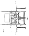
- Figure 2 is an end view of the electronic apparatus manufacturing cell
- Figure 3 is an overhead plan view of the electronic apparatus manufacturing cell
- Figure 4 is an overheard plan view of the electronic apparatus manufacturing cell showing an electronic apparatus at the entry end of the infeed conveyor;
- Figure 5 is an overheard plan view of the electronic apparatus manufacturing cell showing an electronic apparatus at the exit end of the infeed conveyor;
- Figure 6 is an overheard plan view of the electronic apparatus manufacturing cell showing an electronic apparatus at the entry end of the pass conveyor;
- Figure 7 is an overheard plan view of the electronic apparatus manufacturing cell showing an electronic apparatus at the exit end of the pass conveyor;
- Figure 8 is an overheard plan view of the electronic apparatus manufacturing cell showing an electronic apparatus at the entry end of the reject conveyor;
- Figure 9 is an overheard plan view of the electronic apparatus manufacturing cell showing an electronic apparatus at the exit end of the reject conveyor.
- Figure 10 is an overhead plan view of a set of three electronic apparatus manufacturing cells arranged in series.
- Figures 1-3 depict an electronic apparatus manufacturing cell 100 having a lower frame 102 and an upper frame 104.
- Lower frame 102 supports an infeed conveyor 106, a pass conveyor 108 and a reject conveyor 110.
- a transfer robot 112 is disposed above conveyors 106, 108, 110 and is equipped with an end effector suitable for apprehending an electronic apparatus undergoing processing and transferring it from one of conveyors 106, 108, 110 to another of conveyors 106, 108, 110.
- the determination as to the destination conveyor for an electronic apparatus undergoing processing may be made according to the results of tests performed using one or more of stations 114, 116, 118, 120.
- An electronic apparatus is brought into the electronic apparatus manufacturing cell 100 on infeed conveyor 106, processed using one or more of stations 114, 116, 118, 120, and then transferred to the appropriate outfeed conveyor according to the outcome of the processing.
- An electronic apparatus successfully passing through one or more processes performed at one or more of stations 114, 116, 118, 120 may be transferred to pass conveyor 108 and transferred to the next cell in the manufacturing facility.
- An electronic apparatus unsuccessfully completing one or more processes performed at one or more of stations 114, 116, 118, 120 may be transferred to reject conveyor 110 and transferred to the previous cell in the manufacturing facility.
- all of stations 114, 116, 118, 120 may be testing stations. In other embodiments, all of stations 114, 116, 118, 120 may be manufacturing stations. Other embodiments may incorporate a combination of manufacturing stations and testing stations, and certain stations may combine manufacturing capability and testing capability in a single station.
- an electronic apparatus may be processed at a first station 114, 116, 118, 120 and then moved to a second station 114, 116, 118, 120 or a conveyor 108, 110 within electronic apparatus manufacturing cell 100 according to the outcome of the processing at the first station 114, 116, 118, 120.
- An assembly may, for example, be initially moved to station 114, where testing is performed on the assembly. If the testing is successful, the assembly may be moved to station 116 for additional testing or other processing. If the testing is unsuccessful, the assembly may be moved to station 118 for further testing or placed on reject conveyor 110.
- stations 114, 116, 118, 120 are identical to one another, and assemblies are moved to stations 114, 116, 118, 120 according to which of stations 114, 116, 118, 120 are available at a given time.
- stations 114, 116, 118, 120 are specific to certain assembly designs, and an electronic apparatus may be moved to one or more stations 114, 116, 118, 120 within electronic apparatus manufacturing cell 100 according to the type or model of the electronic apparatus. With this capability, a variety of types of electronic apparatuses may be processed within a single apparatus.
- Operator interface panels 122 and 124 will incorporate visual displays and operator input controls such as those shown on operator interface panel 124 in figure 1 .
- Operator interface panels 122 and 124 may also incorporate audio outputs in order to capture the operator's attention when the operator is not looking at the visual display.
- Each of conveyors 106, 108, 110 has the same general construction and each of conveyors 106, 108, 110 is driven independently by a single conveyor motor 130, 132, 134, respectively.
- Each conveyor motor 130, 132, 134 powers a driving jackshaft 140, 142, 144, respectively.
- Each driving jackshaft 140, 142, 144 drives a driven jackshaft 150, 152, 154 through a drive belt 160, 162, 164.
- each pair of driving jackshafts 140, 142, 144 and driven jackshafts 150, 152, 154 impels the payload interface surface (not shown) for each conveyor 106, 108, 110.
- the payload interface surface may vary by application, but will generally be a belt, chain or cable.
- Figures 4 and 5 depict an electronic apparatus 180 entering electronic apparatus manufacturing cell 100 on infeed conveyor 106.
- the electronic apparatus 180 is disposed at the entry end of infeed conveyor 106.
- infeed conveyor 106 will draw electronic apparatus 180 into the central portion of electronic apparatus manufacturing cell 100, where it can be processed.
- Figure 5 shows the position of the electronic apparatus 180 after infeed conveyor 106 has been powered to draw electronic apparatus into the central portion of electronic apparatus manufacturing cell 100.
- electronic apparatus 180 is shown as being generally rectangular, having a longer dimension disposed perpendicularly to the direction of travel of conveyors 106, 108, 110. Alternate embodiments may be designed to accept electronic apparatuses having their longer dimension disposed parallel to the direction of conveyor travel or in some other orientation. Certain embodiments may incorporate a transfer robot 112 having the capability to reorient electronic apparatuses about one or more axes, thereby removing any necessity that the orientation of the incoming electronic apparatuses match the orientation of the stations 114, 116, 118, 120.
- electronic apparatuses such as electronic apparatus 180 may enter electronic apparatus manufacturing cell 100 oriented with their longer axis aligned to the direction of travel of the conveyors, then reoriented by transfer robot 112 to a different orientation matching the orientation of one of stations 114, 116, 118, 120. Subsequent to processing by that station, transfer robot 112 may again reorient electronic apparatus 180 to an orientation matching a different one of stations 114, 116, 118, 120 or one of conveyors 16, 108, 110.
- assemblies entering electronic apparatus manufacturing cell 100 could enter oriented with their longer axis aligned to the direction of travel of the conveyors.
- stations 114, 116, 118 120 which are oriented to interface with assemblies having their longer dimension disposed orthogonally to the direction of travel of the conveyors.
- a wide variety of possibilities will be apparent to those of skill in the art.
- the electronic apparatus 180 is drawn into the electronic apparatus manufacturing cell 100 on infeed conveyor 106, the electronic apparatus is processed using one or more of stations 114, 116, 118, 120. After the processing is complete, a determination may be made as to whether electronic apparatus 180 should be forwarded to the next manufacturing cell via pass conveyor 108 or returned to the prior manufacturing cell via reject conveyor 110. After this determination is made, transfer robot 112 is actuated to move the electronic apparatus to the appropriate outfeed conveyor 108 or 110.
- Figures 6 and 7 show an electronic apparatus 180 disposed on pass conveyor 108.
- the electronic apparatus 180 has been placed on pass conveyor 108 for transfer to the next manufacturing cell.
- Figure 7 shows the position of electronic apparatus 180 after pass conveyor 108 has been actuated in order to transfer electronic apparatus 180 to the next manufacturing cell.
- Figures 8 and 9 show an an electronic apparatus 180 disposed on pass conveyor 108.
- the electronic apparatus 180 has been placed on reject conveyor 110 for transfer to the previous manufacturing cell.
- Figure 9 shows the position of electronic apparatus 180 after reject conveyor 110 has been actuated in order to transfer electronic apparatus 180 to the previous manufacturing cell in the manufacturing line.
- conveyors 106, 108, 110 of each cell 100 extend well beyond the envelopes of a cell defined by the boundaries of frames 102 and 104.
- This design allows electronic apparatus manufacturing cell 100 to be disposed immediately adjacent to the manufacturing cells disposed before and after electronic apparatus manufacturing cell 100 without the need for intermediate conveyor units between the cells.
- Figure 10 shows a set of three processing cells 200, 202, 204 disposed immediately adjacent to one another.
- the frames 102 and 104 of cells 200, 202, 204 define rectangular envelopes 210, 212, 214, respectively.
- the conveyors 106, 108, 110 of each cell 200, 202, 204 extend through the envelope 210, 212, 214 for the cell 200, 202, 204 to the adjacent cell 200, 202, 204.
- Conveyors 106 and 110 of cell 202 for example, extend through side 220 of envelope 212 and up to envelope 210 of cell 200.
- Conveyor 108 of cell 202 extends through side 222 of envelope 212 and up to envelope 214 of cell 204. It can be seen that no additional intermediate conveyors are necessary in order to transfer electronic components between processing cells 200, 202, 204.
Landscapes
- Physics & Mathematics (AREA)
- General Physics & Mathematics (AREA)
- Container, Conveyance, Adherence, Positioning, Of Wafer (AREA)
Abstract
Description
- The present disclosure generally relates to the manufacturing of electronic apparatuses. More particularly, and not by way of any limitation, the present disclosure is directed to a manufacturing cell designed to optimize space within a manufacturing facility.
- Despite significant advances in manufacturing technology, assembly and testing of electronic assemblies require the use of equipment consuming substantial quantities of factory floor space. Testing and characterization of electronic assemblies, for example, generally requires physically large machines, each of which consumes significant floor space within a factory. It is, therefore, desirable to minimize the size and complexity of electronic apparatus manufacturing cells, including electronic assembly testing cells.
- According to a first aspect, the present disclosure relates to an electronic apparatus manufacturing cell defining an electronic apparatus manufacturing cell envelope having a first side and having a second side. The electronic apparatus manufacturing cell comprises an infeed conveyor extending from a point outside of the electronic apparatus manufacturing cell envelope on the first side to a point inside of the envelope and a pass conveyor, extending from a point inside the electronic apparatus manufacturing cell envelope to a point outside of the electronic apparatus manufacturing cell envelope.
- According to a second aspect, the present disclosure relates to an electronic apparatus manufacturing cell defining an electronic apparatus manufacturing cell envelope having a first side and having a second side. The electronic apparatus manufacturing cell comprises an infeed conveyor extending from a point outside of the electronic apparatus manufacturing cell envelope on the first side to a point inside of the envelope, a pass conveyor, extending from a point inside the electronic apparatus manufacturing cell envelope to a point outside of the electronic apparatus manufacturing cell envelope and a reject conveyor, extending from a point inside the electronic apparatus manufacturing cell envelope to a point outside of the electronic apparatus manufacturing cell envelope.
- According to a third aspect, the present disclosure relates to an electronic apparatus manufacturing cell defining an electronic apparatus manufacturing cell envelope having a first side and having a second side. The electronic apparatus manufacturing cell comprises an infeed conveyor extending from a point outside of the electronic assembly manufacturing cell envelope on the first side to a point inside of the envelope, a pass conveyor, extending from a point inside the electronic apparatus manufacturing cell envelope to a point outside of the electronic apparatus manufacturing cell envelope and a reject conveyor, extending from a point inside the electronic apparatus manufacturing cell envelope to a point outside of the electronic apparatus manufacturing cell envelope.
- A more complete understanding of the embodiments of the present disclosure may be had by reference to the following Detailed Description when taken in conjunction with the accompanying drawings wherein:
-
Figure 1 is a front view of an electronic apparatus manufacturing cell; -
Figure 2 is an end view of the electronic apparatus manufacturing cell; -
Figure 3 is an overhead plan view of the electronic apparatus manufacturing cell; -
Figure 4 is an overheard plan view of the electronic apparatus manufacturing cell showing an electronic apparatus at the entry end of the infeed conveyor; -
Figure 5 is an overheard plan view of the electronic apparatus manufacturing cell showing an electronic apparatus at the exit end of the infeed conveyor; -
Figure 6 is an overheard plan view of the electronic apparatus manufacturing cell showing an electronic apparatus at the entry end of the pass conveyor; -
Figure 7 is an overheard plan view of the electronic apparatus manufacturing cell showing an electronic apparatus at the exit end of the pass conveyor; -
Figure 8 is an overheard plan view of the electronic apparatus manufacturing cell showing an electronic apparatus at the entry end of the reject conveyor; -
Figure 9 is an overheard plan view of the electronic apparatus manufacturing cell showing an electronic apparatus at the exit end of the reject conveyor; and -
Figure 10 is an overhead plan view of a set of three electronic apparatus manufacturing cells arranged in series. - An apparatus of the present disclosure will now be described with reference to various examples of how the embodiments can best be made and used. Identical reference numerals are used throughout the description and several views of the drawings to indicate identical or corresponding parts, wherein the various elements are not necessarily drawn to scale.
-
Figures 1-3 depict an electronicapparatus manufacturing cell 100 having alower frame 102 and anupper frame 104.Lower frame 102 supports aninfeed conveyor 106, apass conveyor 108 and areject conveyor 110. Atransfer robot 112 is disposed aboveconveyors conveyors conveyors - The determination as to the destination conveyor for an electronic apparatus undergoing processing may be made according to the results of tests performed using one or more of
stations apparatus manufacturing cell 100 oninfeed conveyor 106, processed using one or more ofstations stations conveyor 108 and transferred to the next cell in the manufacturing facility. An electronic apparatus unsuccessfully completing one or more processes performed at one or more ofstations conveyor 110 and transferred to the previous cell in the manufacturing facility. In certain embodiments, all ofstations stations - In certain embodiments, an electronic apparatus may be processed at a
first station second station conveyor apparatus manufacturing cell 100 according to the outcome of the processing at thefirst station station 114, where testing is performed on the assembly. If the testing is successful, the assembly may be moved tostation 116 for additional testing or other processing. If the testing is unsuccessful, the assembly may be moved tostation 118 for further testing or placed onreject conveyor 110. A wide variety of other possibilities will be apparent to those of skill in the art. - In certain embodiments, all assemblies passing through electronic
apparatus manufacturing cell 100 must pass through each ofstations stations stations stations stations more stations apparatus manufacturing cell 100 according to the type or model of the electronic apparatus. With this capability, a variety of types of electronic apparatuses may be processed within a single apparatus. - Electronic
apparatus manufacturing cell 100 interacts with its human operators viaoperator interface panels operator interface panels operator interface panel 124 infigure 1 .Operator interface panels - Each of
conveyors conveyors single conveyor motor conveyor motor jackshaft jackshaft drive belt jackshafts jackshafts conveyor -
Figures 4 and 5 depict anelectronic apparatus 180 entering electronicapparatus manufacturing cell 100 oninfeed conveyor 106. Infigure 4 , theelectronic apparatus 180 is disposed at the entry end of infeedconveyor 106. In normal operation, infeedconveyor 106 will drawelectronic apparatus 180 into the central portion of electronicapparatus manufacturing cell 100, where it can be processed.Figure 5 shows the position of theelectronic apparatus 180 after infeedconveyor 106 has been powered to draw electronic apparatus into the central portion of electronicapparatus manufacturing cell 100. - Those of skill in the art will note that
electronic apparatus 180 is shown as being generally rectangular, having a longer dimension disposed perpendicularly to the direction of travel ofconveyors transfer robot 112 having the capability to reorient electronic apparatuses about one or more axes, thereby removing any necessity that the orientation of the incoming electronic apparatuses match the orientation of thestations electronic apparatus 180 may enter electronicapparatus manufacturing cell 100 oriented with their longer axis aligned to the direction of travel of the conveyors, then reoriented bytransfer robot 112 to a different orientation matching the orientation of one ofstations transfer robot 112 may again reorientelectronic apparatus 180 to an orientation matching a different one ofstations conveyors apparatus manufacturing cell 100 could enter oriented with their longer axis aligned to the direction of travel of the conveyors. In this case, they may not be properly oriented to interface withstations stations conveyors - After the
electronic apparatus 180 is drawn into the electronicapparatus manufacturing cell 100 oninfeed conveyor 106, the electronic apparatus is processed using one or more ofstations electronic apparatus 180 should be forwarded to the next manufacturing cell viapass conveyor 108 or returned to the prior manufacturing cell viareject conveyor 110. After this determination is made,transfer robot 112 is actuated to move the electronic apparatus to theappropriate outfeed conveyor -
Figures 6 and 7 show anelectronic apparatus 180 disposed onpass conveyor 108. Infigure 6 , theelectronic apparatus 180 has been placed onpass conveyor 108 for transfer to the next manufacturing cell.Figure 7 shows the position ofelectronic apparatus 180 afterpass conveyor 108 has been actuated in order to transferelectronic apparatus 180 to the next manufacturing cell. -
Figures 8 and 9 show an anelectronic apparatus 180 disposed onpass conveyor 108. Infigure 8 , theelectronic apparatus 180 has been placed onreject conveyor 110 for transfer to the previous manufacturing cell.Figure 9 shows the position ofelectronic apparatus 180 afterreject conveyor 110 has been actuated in order to transferelectronic apparatus 180 to the previous manufacturing cell in the manufacturing line. - Those of skill in the art will note that
conveyors cell 100 extend well beyond the envelopes of a cell defined by the boundaries offrames apparatus manufacturing cell 100 to be disposed immediately adjacent to the manufacturing cells disposed before and after electronicapparatus manufacturing cell 100 without the need for intermediate conveyor units between the cells.Figure 10 shows a set of three processingcells frames cells rectangular envelopes conveyors cell envelope cell adjacent cell Conveyors cell 202, for example, extend throughside 220 ofenvelope 212 and up toenvelope 210 ofcell 200.Conveyor 108 ofcell 202 extends throughside 222 ofenvelope 212 and up toenvelope 214 ofcell 204. It can be seen that no additional intermediate conveyors are necessary in order to transfer electronic components betweenprocessing cells - It is believed that the operation and construction of the embodiments of the present disclosure will be apparent from the Detailed Description set forth above. While the exemplary embodiments shown and described may have been characterized as being preferred, it should be readily understood that various changes and modifications could be made therein without departing from the scope of the present disclosure as set forth in the following claims.
Claims (20)
- An electronic apparatus manufacturing cell (100) defining an electronic apparatus manufacturing cell envelope having a first side and a second side, the electronic apparatus manufacturing cell (100) comprising:an infeed conveyor (106) extending from a point outside of the electronic apparatus manufacturing cell envelope on the first side to a point inside of the envelope; anda pass conveyor (108), extending from a point inside the electronic apparatus manufacturing cell envelope to a point outside of the electronic apparatus manufacturing cell envelope.
- The electronic apparatus manufacturing cell (100) of claim 1 wherein the cell comprises at least one processing station (114, 116, 118, 120).
- The electronic apparatus manufacturing cell (100) of claim 1 wherein the cell comprises two or more processing stations (114, 116, 118, 120).
- The electronic apparatus manufacturing cell (100) of claim 1 wherein the cell comprises four processing stations (114, 116, 118, 120).
- The electronic apparatus manufacturing cell (100) of claim 1 wherein the cell (100) comprises an actuator (112) having an end effector secured thereto, operable to move an electronic apparatus from one of the conveyors (106, 108) to a different one of the conveyors (106, 108).
- The electronic apparatus manufacturing cell (100) of claim 1 wherein the electronic apparatus manufacturing cell envelope comprises a generally-rectangular shape.
- The electronic apparatus manufacturing cell (100) of claim 1 wherein the electronic apparatus manufacturing cell envelope has six sides, and wherein the first side and second side have generally-rectangular shapes.
- An electronic apparatus manufacturing cell (100) defining an electronic apparatus manufacturing cell envelope having a first side and having a second side, the electronic apparatus manufacturing cell (100) comprising:an infeed conveyor (106) extending from a point outside of the electronic apparatus manufacturing cell envelope on the first side to a point inside of the envelope;a pass conveyor (108), extending from a point inside the electronic apparatus manufacturing cell envelope to a point outside of the electronic apparatus manufacturing cell envelope on the second side; anda reject conveyor (110), extending from a point inside the electronic apparatus manufacturing cell envelope to a point outside of the electronic apparatus manufacturing cell envelope.
- The electronic apparatus manufacturing cell (100) of claim 8 wherein the cell comprises at least one processing station (114, 116, 118, 120).
- The electronic apparatus manufacturing cell (100) of claim 8 wherein the cell comprises two or more processing stations (114, 116, 118, 120).
- The electronic apparatus manufacturing cell (100) of claim 8 wherein the cell comprises four processing stations (114, 116, 118, 120).
- The electronic apparatus manufacturing cell (100) of claim 8 wherein the cell comprises an actuator (112) having an end effector secured thereto, operable to move an electronic apparatus from one of the conveyors (106, 108, 110) to a different one of the conveyors (106, 108, 110).
- The electronic apparatus manufacturing cell (100) of claim 8 wherein the electronic apparatus manufacturing cell envelope comprises a generally-rectangular shape.
- The electronic apparatus manufacturing cell (100) of claim 8 wherein the electronic apparatus manufacturing cell envelope has six sides, and wherein the first side and second side have generally-rectangular shapes.
- An electronic apparatus manufacturing cell (100) defining an electronic apparatus manufacturing cell envelope having a first side and a second side, the electronic apparatus manufacturing cell comprising:an infeed conveyor (106) extending from a point outside of the electronic apparatus manufacturing cell envelope on the first side to a point inside of the envelope;a pass conveyor (108), disposed adjacent to the infeed conveyor (106), extending from a point inside the electronic apparatus manufacturing cell envelope to a point outside of the electronic apparatus manufacturing cell envelope; anda reject conveyor (110), disposed adjacent to the infeed conveyor (106), extending from a point inside the electronic apparatus manufacturing cell envelope to a point outside of the electronic apparatus manufacturing cell envelope.
- The electronic apparatus manufacturing cell (100) of claim 15 wherein the cell (100) comprises at least one processing station (114, 116, 118, 120).
- The electronic apparatus manufacturing cell (100) of claim 15 wherein the cell comprises two or more processing stations (114, 116, 118, 120).
- The electronic apparatus manufacturing cell (100) of claim 15 wherein the cell (100) comprises four processing stations (114, 116, 118, 120).
- The electronic apparatus manufacturing cell (100) of claim 15 wherein the cell (100) comprises an actuator (112) having an end effector secured thereto, operable to move an electronic apparatus from one of the conveyors (106, 108, 110) to a different one of the conveyors (106, 108, 110).
- The electronic apparatus manufacturing cell (100) of claim 15 wherein the electronic apparatus manufacturing cell envelope comprises a generally-rectangular shape.
Priority Applications (2)
| Application Number | Priority Date | Filing Date | Title |
|---|---|---|---|
| EP07110005.1A EP2003459B1 (en) | 2007-06-11 | 2007-06-11 | Apparatus for manufacture of electronic assemblies |
| CA2634852A CA2634852C (en) | 2007-06-11 | 2008-06-11 | Apparatus for manufacture of electronic assemblies |
Applications Claiming Priority (1)
| Application Number | Priority Date | Filing Date | Title |
|---|---|---|---|
| EP07110005.1A EP2003459B1 (en) | 2007-06-11 | 2007-06-11 | Apparatus for manufacture of electronic assemblies |
Publications (2)
| Publication Number | Publication Date |
|---|---|
| EP2003459A1 true EP2003459A1 (en) | 2008-12-17 |
| EP2003459B1 EP2003459B1 (en) | 2019-08-28 |
Family
ID=38606434
Family Applications (1)
| Application Number | Title | Priority Date | Filing Date |
|---|---|---|---|
| EP07110005.1A Active EP2003459B1 (en) | 2007-06-11 | 2007-06-11 | Apparatus for manufacture of electronic assemblies |
Country Status (2)
| Country | Link |
|---|---|
| EP (1) | EP2003459B1 (en) |
| CA (1) | CA2634852C (en) |
Families Citing this family (1)
| Publication number | Priority date | Publication date | Assignee | Title |
|---|---|---|---|---|
| CN108622598A (en) * | 2017-03-18 | 2018-10-09 | 惠州信兴荣电业塑胶有限公司 | A kind of changeover plug automatic production line |
Citations (1)
| Publication number | Priority date | Publication date | Assignee | Title |
|---|---|---|---|---|
| DE19617537C1 (en) | 1996-05-02 | 1997-07-31 | Telefunken Microelectron | Functional test and measurement device for transponders e.g. as used for motor vehicle access verification systems |
Family Cites Families (1)
| Publication number | Priority date | Publication date | Assignee | Title |
|---|---|---|---|---|
| US20060283688A1 (en) * | 2005-06-10 | 2006-12-21 | Applied Materials, Inc. | Substrate handling system |
-
2007
- 2007-06-11 EP EP07110005.1A patent/EP2003459B1/en active Active
-
2008
- 2008-06-11 CA CA2634852A patent/CA2634852C/en active Active
Patent Citations (1)
| Publication number | Priority date | Publication date | Assignee | Title |
|---|---|---|---|---|
| DE19617537C1 (en) | 1996-05-02 | 1997-07-31 | Telefunken Microelectron | Functional test and measurement device for transponders e.g. as used for motor vehicle access verification systems |
Also Published As
| Publication number | Publication date |
|---|---|
| CA2634852A1 (en) | 2008-12-11 |
| EP2003459B1 (en) | 2019-08-28 |
| CA2634852C (en) | 2013-10-22 |
Similar Documents
| Publication | Publication Date | Title |
|---|---|---|
| CN109581135B (en) | Automatic product testing device and method | |
| KR101402364B1 (en) | Automatic assembly device for cresent bracket | |
| CN104914117A (en) | An X-ray detector and a detection method using the X-ray detector | |
| CN215268191U (en) | Automatic test equipment of connector | |
| CN101995526A (en) | Apparatus for characteristic inspection and sorting of electronic component | |
| CN106903069B (en) | X-ray detection equipment | |
| US8132317B2 (en) | Apparatus for manufacture of electronic assemblies | |
| CA2634852C (en) | Apparatus for manufacture of electronic assemblies | |
| CN214918263U (en) | Automatic code recognition equipment is swept in weighing | |
| KR100740010B1 (en) | Inspection system of display panel | |
| CN113146242A (en) | Motor gearbox seat assembling equipment and assembling method thereof | |
| CN100447624C (en) | Pressure defoaming furnace and pressure defoaming furnace system | |
| KR101771544B1 (en) | Pin auto insertion apparatus for electronic component | |
| CN111049702B (en) | Network terminal verification equipment | |
| CN114346671A (en) | Sliding door and window processing production line equipment and sliding door and window processing and production method | |
| CN220483678U (en) | Full-automatic IR hole film attaching machine | |
| KR100306303B1 (en) | Lcd handler | |
| KR100906364B1 (en) | Work feed and alignment device | |
| CN217528320U (en) | Test assembly line and test system | |
| CN206609940U (en) | A kind of FPC soft boards electric logging equipment | |
| CN219717683U (en) | A low-voltage distribution cabinet drawer production line | |
| CN208385576U (en) | Battery pack automates disassembling apparatus | |
| CN100350568C (en) | Cluster type asher equipment used for manufacture of semiconductor device | |
| CN208086763U (en) | A kind of test equipment | |
| CN221796200U (en) | Turnover device and laser repair device |
Legal Events
| Date | Code | Title | Description |
|---|---|---|---|
| PUAI | Public reference made under article 153(3) epc to a published international application that has entered the european phase |
Free format text: ORIGINAL CODE: 0009012 |
|
| 17P | Request for examination filed |
Effective date: 20070613 |
|
| AK | Designated contracting states |
Kind code of ref document: A1 Designated state(s): AT BE BG CH CY CZ DE DK EE ES FI FR GB GR HU IE IS IT LI LT LU LV MC MT NL PL PT RO SE SI SK TR |
|
| AX | Request for extension of the european patent |
Extension state: AL BA HR MK RS |
|
| AKX | Designation fees paid |
Designated state(s): AT BE BG CH CY CZ DE DK EE ES FI FR GB GR HU IE IS IT LI LT LU LV MC MT NL PL PT RO SE SI SK TR |
|
| RAP1 | Party data changed (applicant data changed or rights of an application transferred) |
Owner name: BLACKBERRY LIMITED |
|
| RAP1 | Party data changed (applicant data changed or rights of an application transferred) |
Owner name: BLACKBERRY LIMITED |
|
| 17Q | First examination report despatched |
Effective date: 20151111 |
|
| STAA | Information on the status of an ep patent application or granted ep patent |
Free format text: STATUS: EXAMINATION IS IN PROGRESS |
|
| GRAP | Despatch of communication of intention to grant a patent |
Free format text: ORIGINAL CODE: EPIDOSNIGR1 |
|
| STAA | Information on the status of an ep patent application or granted ep patent |
Free format text: STATUS: GRANT OF PATENT IS INTENDED |
|
| INTG | Intention to grant announced |
Effective date: 20190403 |
|
| GRAS | Grant fee paid |
Free format text: ORIGINAL CODE: EPIDOSNIGR3 |
|
| GRAA | (expected) grant |
Free format text: ORIGINAL CODE: 0009210 |
|
| STAA | Information on the status of an ep patent application or granted ep patent |
Free format text: STATUS: THE PATENT HAS BEEN GRANTED |
|
| AK | Designated contracting states |
Kind code of ref document: B1 Designated state(s): AT BE BG CH CY CZ DE DK EE ES FI FR GB GR HU IE IS IT LI LT LU LV MC MT NL PL PT RO SE SI SK TR |
|
| REG | Reference to a national code |
Ref country code: GB Ref legal event code: FG4D |
|
| REG | Reference to a national code |
Ref country code: CH Ref legal event code: EP |
|
| REG | Reference to a national code |
Ref country code: AT Ref legal event code: REF Ref document number: 1173059 Country of ref document: AT Kind code of ref document: T Effective date: 20190915 |
|
| REG | Reference to a national code |
Ref country code: IE Ref legal event code: FG4D |
|
| REG | Reference to a national code |
Ref country code: DE Ref legal event code: R096 Ref document number: 602007059109 Country of ref document: DE |
|
| REG | Reference to a national code |
Ref country code: NL Ref legal event code: MP Effective date: 20190828 |
|
| REG | Reference to a national code |
Ref country code: LT Ref legal event code: MG4D |
|
| PG25 | Lapsed in a contracting state [announced via postgrant information from national office to epo] |
Ref country code: FI Free format text: LAPSE BECAUSE OF FAILURE TO SUBMIT A TRANSLATION OF THE DESCRIPTION OR TO PAY THE FEE WITHIN THE PRESCRIBED TIME-LIMIT Effective date: 20190828 Ref country code: NL Free format text: LAPSE BECAUSE OF FAILURE TO SUBMIT A TRANSLATION OF THE DESCRIPTION OR TO PAY THE FEE WITHIN THE PRESCRIBED TIME-LIMIT Effective date: 20190828 Ref country code: BG Free format text: LAPSE BECAUSE OF FAILURE TO SUBMIT A TRANSLATION OF THE DESCRIPTION OR TO PAY THE FEE WITHIN THE PRESCRIBED TIME-LIMIT Effective date: 20191128 Ref country code: LT Free format text: LAPSE BECAUSE OF FAILURE TO SUBMIT A TRANSLATION OF THE DESCRIPTION OR TO PAY THE FEE WITHIN THE PRESCRIBED TIME-LIMIT Effective date: 20190828 Ref country code: SE Free format text: LAPSE BECAUSE OF FAILURE TO SUBMIT A TRANSLATION OF THE DESCRIPTION OR TO PAY THE FEE WITHIN THE PRESCRIBED TIME-LIMIT Effective date: 20190828 Ref country code: PT Free format text: LAPSE BECAUSE OF FAILURE TO SUBMIT A TRANSLATION OF THE DESCRIPTION OR TO PAY THE FEE WITHIN THE PRESCRIBED TIME-LIMIT Effective date: 20191230 |
|
| PG25 | Lapsed in a contracting state [announced via postgrant information from national office to epo] |
Ref country code: IS Free format text: LAPSE BECAUSE OF FAILURE TO SUBMIT A TRANSLATION OF THE DESCRIPTION OR TO PAY THE FEE WITHIN THE PRESCRIBED TIME-LIMIT Effective date: 20191228 Ref country code: ES Free format text: LAPSE BECAUSE OF FAILURE TO SUBMIT A TRANSLATION OF THE DESCRIPTION OR TO PAY THE FEE WITHIN THE PRESCRIBED TIME-LIMIT Effective date: 20190828 Ref country code: GR Free format text: LAPSE BECAUSE OF FAILURE TO SUBMIT A TRANSLATION OF THE DESCRIPTION OR TO PAY THE FEE WITHIN THE PRESCRIBED TIME-LIMIT Effective date: 20191129 Ref country code: LV Free format text: LAPSE BECAUSE OF FAILURE TO SUBMIT A TRANSLATION OF THE DESCRIPTION OR TO PAY THE FEE WITHIN THE PRESCRIBED TIME-LIMIT Effective date: 20190828 |
|
| REG | Reference to a national code |
Ref country code: AT Ref legal event code: MK05 Ref document number: 1173059 Country of ref document: AT Kind code of ref document: T Effective date: 20190828 |
|
| PG25 | Lapsed in a contracting state [announced via postgrant information from national office to epo] |
Ref country code: TR Free format text: LAPSE BECAUSE OF FAILURE TO SUBMIT A TRANSLATION OF THE DESCRIPTION OR TO PAY THE FEE WITHIN THE PRESCRIBED TIME-LIMIT Effective date: 20190828 |
|
| PG25 | Lapsed in a contracting state [announced via postgrant information from national office to epo] |
Ref country code: RO Free format text: LAPSE BECAUSE OF FAILURE TO SUBMIT A TRANSLATION OF THE DESCRIPTION OR TO PAY THE FEE WITHIN THE PRESCRIBED TIME-LIMIT Effective date: 20190828 Ref country code: DK Free format text: LAPSE BECAUSE OF FAILURE TO SUBMIT A TRANSLATION OF THE DESCRIPTION OR TO PAY THE FEE WITHIN THE PRESCRIBED TIME-LIMIT Effective date: 20190828 Ref country code: IT Free format text: LAPSE BECAUSE OF FAILURE TO SUBMIT A TRANSLATION OF THE DESCRIPTION OR TO PAY THE FEE WITHIN THE PRESCRIBED TIME-LIMIT Effective date: 20190828 Ref country code: AT Free format text: LAPSE BECAUSE OF FAILURE TO SUBMIT A TRANSLATION OF THE DESCRIPTION OR TO PAY THE FEE WITHIN THE PRESCRIBED TIME-LIMIT Effective date: 20190828 Ref country code: EE Free format text: LAPSE BECAUSE OF FAILURE TO SUBMIT A TRANSLATION OF THE DESCRIPTION OR TO PAY THE FEE WITHIN THE PRESCRIBED TIME-LIMIT Effective date: 20190828 Ref country code: PL Free format text: LAPSE BECAUSE OF FAILURE TO SUBMIT A TRANSLATION OF THE DESCRIPTION OR TO PAY THE FEE WITHIN THE PRESCRIBED TIME-LIMIT Effective date: 20190828 |
|
| PG25 | Lapsed in a contracting state [announced via postgrant information from national office to epo] |
Ref country code: IS Free format text: LAPSE BECAUSE OF FAILURE TO SUBMIT A TRANSLATION OF THE DESCRIPTION OR TO PAY THE FEE WITHIN THE PRESCRIBED TIME-LIMIT Effective date: 20200224 Ref country code: SK Free format text: LAPSE BECAUSE OF FAILURE TO SUBMIT A TRANSLATION OF THE DESCRIPTION OR TO PAY THE FEE WITHIN THE PRESCRIBED TIME-LIMIT Effective date: 20190828 Ref country code: CZ Free format text: LAPSE BECAUSE OF FAILURE TO SUBMIT A TRANSLATION OF THE DESCRIPTION OR TO PAY THE FEE WITHIN THE PRESCRIBED TIME-LIMIT Effective date: 20190828 |
|
| REG | Reference to a national code |
Ref country code: DE Ref legal event code: R097 Ref document number: 602007059109 Country of ref document: DE |
|
| PLBE | No opposition filed within time limit |
Free format text: ORIGINAL CODE: 0009261 |
|
| STAA | Information on the status of an ep patent application or granted ep patent |
Free format text: STATUS: NO OPPOSITION FILED WITHIN TIME LIMIT |
|
| PG2D | Information on lapse in contracting state deleted |
Ref country code: IS |
|
| 26N | No opposition filed |
Effective date: 20200603 |
|
| PG25 | Lapsed in a contracting state [announced via postgrant information from national office to epo] |
Ref country code: SI Free format text: LAPSE BECAUSE OF FAILURE TO SUBMIT A TRANSLATION OF THE DESCRIPTION OR TO PAY THE FEE WITHIN THE PRESCRIBED TIME-LIMIT Effective date: 20190828 |
|
| PG25 | Lapsed in a contracting state [announced via postgrant information from national office to epo] |
Ref country code: MC Free format text: LAPSE BECAUSE OF FAILURE TO SUBMIT A TRANSLATION OF THE DESCRIPTION OR TO PAY THE FEE WITHIN THE PRESCRIBED TIME-LIMIT Effective date: 20190828 |
|
| REG | Reference to a national code |
Ref country code: CH Ref legal event code: PL |
|
| PG25 | Lapsed in a contracting state [announced via postgrant information from national office to epo] |
Ref country code: LU Free format text: LAPSE BECAUSE OF NON-PAYMENT OF DUE FEES Effective date: 20200611 |
|
| REG | Reference to a national code |
Ref country code: BE Ref legal event code: MM Effective date: 20200630 |
|
| PG25 | Lapsed in a contracting state [announced via postgrant information from national office to epo] |
Ref country code: LI Free format text: LAPSE BECAUSE OF NON-PAYMENT OF DUE FEES Effective date: 20200630 Ref country code: IE Free format text: LAPSE BECAUSE OF NON-PAYMENT OF DUE FEES Effective date: 20200611 Ref country code: CH Free format text: LAPSE BECAUSE OF NON-PAYMENT OF DUE FEES Effective date: 20200630 |
|
| PG25 | Lapsed in a contracting state [announced via postgrant information from national office to epo] |
Ref country code: BE Free format text: LAPSE BECAUSE OF NON-PAYMENT OF DUE FEES Effective date: 20200630 |
|
| PG25 | Lapsed in a contracting state [announced via postgrant information from national office to epo] |
Ref country code: MT Free format text: LAPSE BECAUSE OF FAILURE TO SUBMIT A TRANSLATION OF THE DESCRIPTION OR TO PAY THE FEE WITHIN THE PRESCRIBED TIME-LIMIT Effective date: 20190828 Ref country code: CY Free format text: LAPSE BECAUSE OF FAILURE TO SUBMIT A TRANSLATION OF THE DESCRIPTION OR TO PAY THE FEE WITHIN THE PRESCRIBED TIME-LIMIT Effective date: 20190828 |
|
| REG | Reference to a national code |
Ref country code: DE Ref legal event code: R082 Ref document number: 602007059109 Country of ref document: DE Ref country code: DE Ref legal event code: R081 Ref document number: 602007059109 Country of ref document: DE Owner name: MALIKIE INNOVATIONS LTD., IE Free format text: FORMER OWNER: BLACKBERRY LIMITED, WATERLOO, ONTARIO, CA |
|
| PGFP | Annual fee paid to national office [announced via postgrant information from national office to epo] |
Ref country code: DE Payment date: 20250626 Year of fee payment: 19 |
|
| PGFP | Annual fee paid to national office [announced via postgrant information from national office to epo] |
Ref country code: GB Payment date: 20250617 Year of fee payment: 19 |
|
| PGFP | Annual fee paid to national office [announced via postgrant information from national office to epo] |
Ref country code: FR Payment date: 20250624 Year of fee payment: 19 |