EP2000848B1 - Guide d'onde optoélectronique à semi-conducteur - Google Patents
Guide d'onde optoélectronique à semi-conducteur Download PDFInfo
- Publication number
- EP2000848B1 EP2000848B1 EP08017012A EP08017012A EP2000848B1 EP 2000848 B1 EP2000848 B1 EP 2000848B1 EP 08017012 A EP08017012 A EP 08017012A EP 08017012 A EP08017012 A EP 08017012A EP 2000848 B1 EP2000848 B1 EP 2000848B1
- Authority
- EP
- European Patent Office
- Prior art keywords
- semiconductor
- type
- layer
- clad layer
- waveguide
- Prior art date
- Legal status (The legal status is an assumption and is not a legal conclusion. Google has not performed a legal analysis and makes no representation as to the accuracy of the status listed.)
- Expired - Fee Related
Links
- 239000004065 semiconductor Substances 0.000 title claims description 275
- 230000005693 optoelectronics Effects 0.000 title claims description 87
- 239000010410 layer Substances 0.000 claims description 332
- 239000012792 core layer Substances 0.000 claims description 70
- 238000002955 isolation Methods 0.000 claims description 55
- 230000003287 optical effect Effects 0.000 description 88
- 230000004888 barrier function Effects 0.000 description 16
- 230000031700 light absorption Effects 0.000 description 15
- 230000005540 biological transmission Effects 0.000 description 13
- 230000008859 change Effects 0.000 description 12
- 238000010586 diagram Methods 0.000 description 12
- 238000005468 ion implantation Methods 0.000 description 11
- 238000005036 potential barrier Methods 0.000 description 11
- 229910003327 LiNbO3 Inorganic materials 0.000 description 10
- 239000000463 material Substances 0.000 description 8
- 239000000370 acceptor Substances 0.000 description 7
- 150000001875 compounds Chemical class 0.000 description 7
- 238000004519 manufacturing process Methods 0.000 description 7
- 230000000694 effects Effects 0.000 description 6
- 230000005684 electric field Effects 0.000 description 6
- 239000000203 mixture Substances 0.000 description 6
- 239000002019 doping agent Substances 0.000 description 5
- 238000005530 etching Methods 0.000 description 5
- 239000012535 impurity Substances 0.000 description 5
- 238000000926 separation method Methods 0.000 description 5
- 230000003247 decreasing effect Effects 0.000 description 4
- 238000000034 method Methods 0.000 description 4
- 230000006798 recombination Effects 0.000 description 4
- 238000005215 recombination Methods 0.000 description 4
- 239000000758 substrate Substances 0.000 description 4
- 229910000980 Aluminium gallium arsenide Inorganic materials 0.000 description 3
- 229910001218 Gallium arsenide Inorganic materials 0.000 description 3
- 239000000969 carrier Substances 0.000 description 3
- 238000002347 injection Methods 0.000 description 3
- 239000007924 injection Substances 0.000 description 3
- 230000003071 parasitic effect Effects 0.000 description 3
- 230000009467 reduction Effects 0.000 description 3
- 238000009825 accumulation Methods 0.000 description 2
- 125000004429 atom Chemical group 0.000 description 2
- 230000015572 biosynthetic process Effects 0.000 description 2
- 230000007547 defect Effects 0.000 description 2
- 239000006185 dispersion Substances 0.000 description 2
- 238000005516 engineering process Methods 0.000 description 2
- 125000005842 heteroatom Chemical group 0.000 description 2
- 150000002500 ions Chemical class 0.000 description 2
- 239000002184 metal Substances 0.000 description 2
- 238000010521 absorption reaction Methods 0.000 description 1
- 230000002411 adverse Effects 0.000 description 1
- 238000005452 bending Methods 0.000 description 1
- 239000003989 dielectric material Substances 0.000 description 1
- 238000009826 distribution Methods 0.000 description 1
- 239000000835 fiber Substances 0.000 description 1
- 230000001939 inductive effect Effects 0.000 description 1
- 230000010363 phase shift Effects 0.000 description 1
- 238000000206 photolithography Methods 0.000 description 1
- 230000000704 physical effect Effects 0.000 description 1
- 230000008569 process Effects 0.000 description 1
- 230000004044 response Effects 0.000 description 1
- 230000000087 stabilizing effect Effects 0.000 description 1
- 238000006467 substitution reaction Methods 0.000 description 1
Images


Classifications
-
- G—PHYSICS
- G02—OPTICS
- G02F—OPTICAL DEVICES OR ARRANGEMENTS FOR THE CONTROL OF LIGHT BY MODIFICATION OF THE OPTICAL PROPERTIES OF THE MEDIA OF THE ELEMENTS INVOLVED THEREIN; NON-LINEAR OPTICS; FREQUENCY-CHANGING OF LIGHT; OPTICAL LOGIC ELEMENTS; OPTICAL ANALOGUE/DIGITAL CONVERTERS
- G02F1/00—Devices or arrangements for the control of the intensity, colour, phase, polarisation or direction of light arriving from an independent light source, e.g. switching, gating or modulating; Non-linear optics
- G02F1/01—Devices or arrangements for the control of the intensity, colour, phase, polarisation or direction of light arriving from an independent light source, e.g. switching, gating or modulating; Non-linear optics for the control of the intensity, phase, polarisation or colour
- G02F1/015—Devices or arrangements for the control of the intensity, colour, phase, polarisation or direction of light arriving from an independent light source, e.g. switching, gating or modulating; Non-linear optics for the control of the intensity, phase, polarisation or colour based on semiconductor elements having potential barriers, e.g. having a PN or PIN junction
- G02F1/017—Structures with periodic or quasi periodic potential variation, e.g. superlattices, quantum wells
- G02F1/01708—Structures with periodic or quasi periodic potential variation, e.g. superlattices, quantum wells in an optical wavequide structure
-
- B—PERFORMING OPERATIONS; TRANSPORTING
- B82—NANOTECHNOLOGY
- B82Y—SPECIFIC USES OR APPLICATIONS OF NANOSTRUCTURES; MEASUREMENT OR ANALYSIS OF NANOSTRUCTURES; MANUFACTURE OR TREATMENT OF NANOSTRUCTURES
- B82Y20/00—Nanooptics, e.g. quantum optics or photonic crystals
Definitions
- the present disclosure relates to a semiconductor optoelectronic waveguide and more specifically to a semiconductor optoelectronic waveguide having an nin-type heterostructure which enables a stable operation of an optical modulator. Further, the present disclosure relates to a semiconductor optoelectronic waveguide having an isolation structure for electrical signal line in an nin-type heterostructure which is used for ultrahigh-speed optical modulation at a long wavelength.
- an optical signal modulated at a high bit rate of Gbit/s or more is transmitted.
- the signal with wavelength chirping is more significantly influenced by the fiber dispersion effects, resulting in distortion of the signal pulse shape. It is, therefore, necessary to use an optical signal which is smaller in wavelength chirping.
- an optical signal is generated not by direct modulation of a laser diode (LD) having an extremely large chirping, but by external modulation combining a continuous-wave operated laser diode (LD).
- a typical external modulator which is used in a long distance optical transmission is an LN modulator configured with LiNbO 3 (LN) optoelectronic waveguide, in which an optical waveguide is coupled to an electrical waveguide.
- LN LiNbO 3
- the operation principle of the LN modulator is based on the change in optical refractive index by electric field in a waveguide due to electro-optical effects, and resulting phase shift of optical signal.
- the above-described LN modulator is able to function as an optical phase modulator, a light intensity modulator in which a Mach Zehnder (MZ) interferometer is incorporated, or an intelligent optical switch constituted by combining many waveguides.
- MZ Mach Zehnder
- LNmodulators still have many problems. Since LiNbO 3 is a dielectric material, a sophisticated manufacturing technology is required in stabilizing the surface of the material and processing a waveguide. It is also necessary to use a special photolithography because of relatively long in waveguide length which is different from that for semiconductor fabrication process. Further, the size of package in which an LN modulator is loaded must be made larger in dimension. Due to these reasons, the LN modulator module is higher in manufacturing cost and an optical transmitter using it is relatively large in dimension, which are problems related to a conventional modulator.
- semiconductor optical modulators the operation principle of which is similar to that of an LN modulator.
- these include a GaAs optical modulator in which a Schottky electrode is placed on a semi-insulating GaAs to configure an optoelectronic waveguide.
- Another one is an InP/InGaAsP optical modulator.
- driving voltage is effectively applied to a core portion of a waveguide through utilization of a hetero pn junction, in addition to good optical confinement.
- the former (LN modulator) has a disadvantage in that electrical loss is large due to a longer waveguide length
- the latter semiconductor-based modulator
- a greater light absorption due to a p clad layer results in a difficulty of designing longer waveguide for realizing low driving voltage.
- proposed is a modulator in which clad layers on both sides of an InP/InGaAsP optical modulator are an n-type (a so-called nin-type structure) (for example, refer to Patent Documents 1 and 2).
- Fig. 9 is a view illustrating a band diagram of the semiconductor optoelectronic waveguide which constitutes a conventional InP/InGaAsP optical modulator.
- the symbol 101 given in the view denotes a core layer of a waveguide; 102-1 and 102-2, first clad layers; 103-1 and 103-2, a p-type and an n-type second clad layers respectively. Further, 100-1 and 100-2 denote respectively electrons and positive holes (holes). Voltage is applied to the p-type second clad layer 103-1 and the n-type second clad layer 103-2 to induce a desired electro-optical effect on the core layer 101, thereby realizing an optical modulation.
- voltage is applied to the core layer 101 by a pn junction, achieving a decreased leak current. Further, carriers generated by light absorption are allowed to flow easily to electrodes, thereby realizing a stable operation.
- a GaAs optical modulator equipped with a Schottky electrode has a problem that an operating voltage is elevated.
- an InP/InGaAsP optical modulator has a problem that an operating bandwidth is narrow due to transmission loss of electrical signals resulting from a higher resistance on a p-type clad layer.
- a greater light absorption in a p-type clad layer makes it difficult to prolong the waveguide length, thereby further reducing the operating voltage of the modulator.
- the transmission loss of electrical signals in the InP/InGaAsP optical modulator appears in the course of charge and discharge by the pn junction through the resistance of signal lines and that of the p-type second clad layer 103-1.
- the resistance of the p-type second clad layer 103-1 originates from physical properties of a material that hole mobility is low it is an unavoidable problem.
- a nin-type waveguide structure has been proposed.
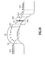
- Fig. 10 is a view showing a band diagram of the nin-type semiconductor optoelectronic waveguide structure.
- the p and n clad layers (103-1 and 103-2) on both sides of the InP/InGaAsP optical waveguide given in a Fig. 9 are changed to those of n-type, and the modulator operation is done by applying voltage between these two n-type electrode layers.
- the symbol 111 given in the figure denotes a core layer of the waveguide, and 112-1 and 112-2 denote the first clad layers. This is different from the constitution given in Fig.
- both of the electrode layers (114-1 and 114-2) are of n-type, and the p-type second clad layer 103-1 given in Fig. 9 is replaced by a Fe-doped semi-insulating layer 115 having deep levels 116 and an n-type electrode layer 114-1 (for example, refer to Patent Document 1).
- the n-type electrode layer 114-2 is corresponding to the n-type second clad layer 103-2 given in Fig. 9
- 110-1 and 110-2 denote respectively electrons and positive holes (holes).
- a semiconductor structure of this kind and fabrication thereof have been discussed by K. Tsuzuki et al., "40 Gbit/s n-i-n InP Mach-Zehnder modulator with a ⁇ voltage of 2.2 V", Electronics Letters, Vol. 39, No. 2, 2 October 2003 .
- a deep Fe level 116 in the semi-insulating layer 115 acts as an ionized acceptor and, therefore, the electrical charge will bend a band to form a potential barrier to electrons.
- electrons 114-1 and holes 110-2 in the vicinity of the curved portion of the band are recombined via the deep Fe level 116 in the semi-insulating layer 115. Therefore, the potential barrier can keep its profile when excess holes are induced, and suppresses leakage current by electron flow from the layer 110 - 1, making it possible to apply an electric field to the core layer 111.
- the density of ionized Fe deep levels changes depending on a bias because the density of the deep levels 116 is not sufficiently high.
- Dependence of such ionization on the bias will cause a change in thickness of a depletion layer, resulting in a failure in keeping a proportional relationship between the applied voltage and the electric field involved in the core layer 111.
- response to high speed modulation signals is difficult due to a relatively long interval of capture and emission of carriers by the deep Fe level 116. In other words, the modulation strength has frequency dispersion.
- Fig. 11 is a diagram illustrating a conventional nin-type semiconductor optical modulator.
- the symbol 121 given in the figure denotes an n-type third semiconductor clad layer; 122, a p-type fifth semiconductor clad layer; 123, a first semiconductor clad layer; 124, a semiconductor core layer having electro-optical effects; 125, a second semiconductor clad layer; 126, an n-type fourth semiconductor clad layer; 127 and 128, n-type electrodes; 129, a grooved electrical isolation region formed by etching.
- Patent Document 1 There is another report about an electrically separated structure in which a semi-insulating semiconductor is grown again on the grooved etched portion (for example, refer to Patent Document 1), which is, however, not necessarily an optimal technique for providing an optical modulator because of the more complicated structure.
- the p-type fifth semiconductor clad layer 122 and the first semiconductor clad layer 123 are sequentially laminated on the n-type third semiconductor clad layer 121, and the semiconductor core layer 124 having electro-optical effects is provided so as to be held between the first semiconductor clad layer 123 and the second semiconductor clad layer 125. Further, on the second semiconductor clad layer 125 is laminated the n-type fourth semiconductor clad layer 126 having the grooved electrical isolation region 129 formed by etching. On the fourth semiconductor clad layer 126 is provided the electrode 128, and on both sides of the raised portion of the third semiconductor clad layer 121 is provided the electrode 127.
- the n-type InP clad layer 126 is partially etched in a grooved form to provide the electrical isolation region 129, an optical transmission mode is changed at a portion where a clad layer is varied in thickness, resulting in optical scattering loss.
- the fourth semiconductor clad layer 126 is etched in a relatively deep manner, posing a problem in controlling the etching.
- a waveguide portion where modulation is conducted and a connecting waveguide portion outside thereof are separated electrically by partially removing a part of the upper layer of the n-type clad layer 126, thereby resulting in formation of a recess 129 on the waveguide.
- This recess poses a problem that optical loss increases in association with a change in the optical transmission mode at portions from a connecting waveguide to an electrical isolation region and at portions from the electrical isolation region to a main waveguide.
- the high resistant clad layer since it is necessary to leave a high resistant clad layer having a certain thickness in the electrical isolation region (recess region), the high resistant clad layer must not be reduced in thickness, thereby making it impossible to effectively apply an electric field to the semiconductor core layer 124, which is a problem.
- An object of the disclosure is to provide a semiconductor optoelectronic waveguide having a nin-type heterostructure which enables the stable operation of an optical modulator.
- Another object of the present disclosure is to provide a semiconductor optoelectronic waveguide which less influences transmission of an optical mode than a conventional recess-forming electrical isolation region to solve a problem of optical loss, and has a structure of electrical isolation region which is well controllable and stable.
- Still another object of the present disclosure is to solve the above-described problem that a core layer undergoes a change in voltage in a semiconductor optoelectronic waveguide such as a nin-type InP/InGaAsP optical modulator, and realize a stable operation of the semiconductor optoelectronic waveguide.
- a semiconductor optoelectronic waveguide such as a nin-type InP/InGaAsP optical modulator
- Patent Document 1 Japanese Patent Application No. 2003-177368
- Patent Document 2 U.S. Patent No. 5,647,029
- a semiconductor optoelectronic waveguide maybe provided with a first semiconductor clad layer arranged on each of one main surface and the other main surface of a semiconductor core layer having electro-optical effects, a second semiconductor clad layer arranged on the first semiconductor clad layer, a pn junction layer arranged on the second semiconductor clad layer laminated on one main surface of the semiconductor core layer in which the second semiconductor clad layer side is a p-type and the side opposed to the second semiconductor clad layer is an n-type, and a third semiconductor clad layer arranged on the pn junction layer and on the second semiconductor clad layer laminated on the other main surface of the semiconductor core layer which functions as an n-type electrode layer, wherein the band gap of the first semiconductor clad layer is greater than that of the semiconductor core layer, and each of the band gap of the second semiconductor clad layer and the third semiconductor clad layer is greater than that of the first semiconductor clad layer.
- the semiconductor optoelectronic waveguide it is possible to easily control a band profile of an nin-type heterostructure equipped by an optoelectronic waveguide and also to provide a semiconductor optoelectronic waveguide which enables a stable operation of an optical modulator. Therefore, it is also possible to realize a more stable optical modulation, without affecting advantageous features of a semiconductor optoelectronic waveguide having the nin-type heterostructure that it can be driven at a lower voltage, thereby contributing to a smaller electric power consumption of a module and a lower manufacturing cost.
- a semiconductor optoelectronic waveguide may be provided with a semiconductor core layer having effective electro-optical effects, a first and a second semiconductor clad layers which vertically hold the semiconductor core layer and whose band gap is greater than that of the semiconductor core layer, a third and a fourth semiconductor clad layers which vertically hold the first and the second semiconductor clad layers and contain an n-type dopant, a fifth semiconductor layer having the first and the third semiconductor clad layers on the substrate side, which is arranged between the first semiconductor clad layer and the third semiconductor clad layer, containing a p-type dopant, and whose band gap is greater than that of the semiconductor core layer, at least one electrical isolation region formed by implanting ions to the fourth semiconductor clad layer to improve the quality of materials, and electrodes individually provided at a major region other than the electrical isolation region of the fourth semiconductor clad layer and at the third semiconductor clad layer, wherein voltage is applied to the semiconductor core layer.
- the semiconductor optoelectronic waveguide of the above example it is possible to provide a semiconductor optoelectronic waveguide which less influences the transmission of an optical mode than a conventional recess-forming electrical isolation region to solve a problem of optical loss and has a structure of the electrical isolation region which is well controllable and stable.
- the present disclosure is also effective in the realization of an optical modulator using an nin-type heterostructure which can be driven at a lower voltage with good structural controllability, thereby contributing to a smaller electric power consumption of an optical modulator module and a lower manufacturing cost of the module through reduction in input optical power.
- the semiconductor optoelectronic waveguide of the present invention is provided with a semiconductor core layer having electro-optical effects, a first and a second semiconductor clad layer arranged below and above the semiconductor core layer, respectively; an n-type third semiconductor clad layer which is arranged below the first semiconductor clad layer; a fourth semiconductor clad layer which is arranged above the second semiconductor clad layer, the fourth semiconductor clad layer having an n-type major region and a p-type isolation region adjacent to the major region inside the fourth clad layer; a p-type fifth semiconductor clad layer arranged between the second semiconductor clad layer and the fourth semiconductor clad layer; an upper electrode in contact with said major region and said isolation region; and another electrode provided on the third semiconductor clad layer, wherein said electrodes are configured to apply a voltage to the semiconductor core layer, and wherein the band gaps of said first, second and fifth semiconductor clad layers are greater than the band gap of the semiconductor core layer.
- the semiconductor optoelectronic waveguide of the present invention it is possible to suppress parasitic bipolar effects of the optoelectronic waveguide using an nin-type heterostructure and consequently to solve a problem that holes accumulated in an p-type barrier layer allow the barrier height to change, thereby causing leak current to change the core layer voltage.
- the semiconductor optoelectronic waveguide of the present invention is also effective in stably realizing good performance of an optical modulator using a nin-type heterostructure characterized in that it can be driven at a lower voltage and also able to allow a higher input optical power and increase the output of an optical transmitter module.
- Fig. 1A and Fig. 1B are configuration diagrams for explaining one example of the semiconductor optoelectronic waveguide.
- Fig. 1A is a perspective view of the optoelectronic waveguide and
- Fig. 1B is a view illustrating the band diagram thereof.
- the symbol 11 given in the figure denotes a semiconductor core layer; 12-1 and 12-2, first semiconductor clad layers arranged on both main surfaces of the semiconductor core layer 11; 13-1 and 13-2, second semiconductor clad layers arranged on each of the first semiconductor clad layers 12-1 and 12-2.
- the symbols 14-1 and 14-2 denote third semiconductor clad layers.
- the symbols 15 and 16 denote respectively a p-type layer and an n-type layer, and a pn junction layer is constituted with these layers of 15 and 16.
- the second semiconductor clad layer 13-1 On the second semiconductor clad layer 13-1 is arranged the p-type layer 15, and on the n-type layer 16 is arranged the third semiconductor clad layer 14-1. Further, under the second semiconductor clad layer 13-2 is arranged the third semiconductor clad layer 14-2.
- the structural (and material) parameters of the core layer 11 are determined in such a way that electro-optical effect is effectively exerted at an operating light wavelength and light absorption does not pose any problem.
- a quantum well layer and a barrier layer are made with InGaAlAs compounds to form a multiple-quantum well structured core layer 11, in which these layers are allowed to be different in Ga/Al compositions.
- intermediate clad layers (12-1 and 12-2) having compositions such as InGaAlAs, whose band gap is greater than that of the core layer 11 so that carriers generated by light absorption are not trapped by a hetero interface.
- clad layers 13-1 and 13-2 having compositions such as InGaAlAs, whose band gap is greater than that of the intermediate clad layer.
- a p-type layer 15 of InGaAlAs and an n-type layer 16 of InGaAlAs are sequentially laminated a p-type layer 15 of InGaAlAs and an n-type layer 16 of InGaAlAs, for example.
- a whole region of the p-type InGaAlAs layer 15 and a part or a whole region of the n-type InGaAlAs layer 16 are depleted. Doping concentration profiles of these layers are determined in such a way that the potential in these depleted regions changes with sufficiently great extent or a sufficient potential barrier to electrons is induced.
- doping concentrations of these layers are 1 ⁇ 10 17 cm -3 or greater for the p-type layer 15 and 5 ⁇ 10 17 cm -3 or greater for the n-type layer 16.
- the doping concentration of the p-type layer 15 is to give 2 ⁇ 10 17 cm -3 and that of the n-type layer 16 is to give 1 ⁇ 10 18 cm -3 .
- n-type layers 14-1 and 14-2 having compositions such as InGaAlAs and functioning as a clad layer.
- an electrode 18-1 On the upper surface of the n-type layer 14-1 is provided an electrode 18-1.
- the band gap of these n-type layers 14-1 and 14-2 is designed to be greater than that of intermediate clad layers 12-1 and 12-2.
- an n-type layer 14-2 which is the bottom layer of the laminated structure, is provided on a partial region of the main surface of an n-type electrode layer 17 having an electrode 18-2.
- the waveguide is to have structures including a mesa structure, the cross section of which is as illustrated in Fig. 1A , and in a state that light is transmitted to the waveguide, an electrical signal is input from electrodes 18-1 and 18-2 to apply voltage between an n-type layer 14-1 and an n-type layer 14-2.
- a potential barrier formed by the presence of the p-type InGaAlAs layer 15 and the n-type InGaAlAs layer 16 suppresses leak current in association with electron injection from the n-type layer 14-1, and positive holes 10-2 generated by light absorption (although in a sparing quantity) are recombined via shallow-level acceptors and donors in the p-type InGaAlAs layer 15 and the n-type InGaAlAs layer 16, by which voltage can be applied to the core layer 11.
- a pn junction layer constituted with the p-type InGaAlAs layer 15 and the n-type InGaAlAs layer 16 is provided between the clad layer 13-1 and the n-type layer 14-1.
- the pn junction layer may be provided between the clad layer 13-2 and the n-type layer 14-2.
- Electrons 10-1 and holes 10-2 are generated by light absorption in the core layer 11 while the device functions, although in a sparing quantity.
- the electrons 10-1 easily reach the n-type layer 14-2, whereas the holes 10-2 may accumulate in the vicinity of the n-type InGaAlAs layer 16 having a steep band bending.
- the accumulation of holes 10-3 is factor to cause a bias sift of forward in a pn junction between the p-type InGaAlAs layer 15 and the n-type InGaAlAs layer 16, thereby pushing down a potential barrier in the region and making it difficult to apply voltage to the core layer 11. Further, they may be responsible for electron injection from the side of the n-type layer 14-1.
- such accumulated positive holes 10-3 are smoothly recombined to give a layer in which the p-type InGaAlAs layer 15 and the n-type InGaAlAs layer 16 are doped at high concentrations, the pn junction is made thinner, by which electrons and accumulated holes are made closer spatially to increase a probability of recombination between the bands indicated by the arrow in Fig. 1B .
- holes 10-3 generated in the core layer 11 and accumulated in the vicinity of the n-type InGaAlAs layer 16 are smoothly removed, making it possible to suppress a change in height of the potential barrier formed by the p-type InGaAlAs layer 15 and the n-type InGaAlAs layer 16.
- an impurity forming a deep level such as Fe is doped to a layer corresponding to the n-type InGaAlAs layer 16 in Fig. 1 , together with a donor impurity. Further, a doped quantity of the impurity forming a deep level is established to be sufficiently lower than that of the donor impurity. According to the thus established doping, an impurity forming a deep level will not give a great influence to a band profile, whereas it elevates a recombination probability via a deep level, thereby making it possible to smoothly remove positive holes generated in the core layer 11 by light absorption.
- Fig. 2 is a view illustrating a band diagram of the semiconductor optoelectronic waveguide of a fourth example of the present disclosure, in which a layer corresponding to the n-type InGaAlAs layer 16 in Fig. 1 is given an n-type layer 19 which is smaller in band gap energy than InGaAsP.
- a band gap difference ( ⁇ E G ) between a p-type layer 15 such as InGaAlAs and an n-type layer 19 such as InGaAsP as well as a doping profile are formed in a desired configuration, by which some of positive holes 10-2 generated inside the core layer 11 by light absorption reach the n-type InGaAsP layer 19 (10-3) to enable a faster recombination.
- valence band discontinuity between the p-type InGaAlAs layer 15 and the n-type InGaAsP layer 19 is smaller than conduction band discontinuity. This is because the smaller the valence band discontinuity is, the more easily the holes pass through an interface between the p-type InGaAlAs layer 15 and the n-type InGaAsP layer 19.
- InGaAlAs and InGaAsP are exemplified as components for the waveguide.
- the present invention is not restricted to these components but the family of III-V compound semiconductors including AlGaAs compounds may be used to constitute the waveguide of the present invention.
- Fig. 3 is a perspective view for explaining a fifth example of the semiconductor optoelectronic waveguide.
- the symbol 21 denotes an n-type third semiconductor clad layer; 22, a p-type fifth semiconductor clad layer; 23, a first semiconductor clad layer; 24, a semiconductor core layer having electro-optical effects; 25, a second semiconductor clad layer; 26, an n-type fourth semiconductor clad layer; 27 and 28, n-type electrodes; 29, an electrical isolation region formed by ion implantation; 29-1, a connection waveguide region of the fourth semiconductor clad layer 26 with the electrical isolation region 29.
- n-type third semiconductor clad layer 21 On the n-type third semiconductor clad layer 21 are sequentially laminated the p-type fifth semiconductor clad layer 22 and the first semiconductor clad layer 23.
- the semiconductor core layer 24 having electro-optical effects are provided so as to be held between the first semiconductor clad layer 23 and the second semiconductor clad layer 25.
- the n-type fourth semiconductor clad layer 26 On the second semiconductor clad layer 25 is laminated the n-type fourth semiconductor clad layer 26 having the electrical isolation region 29 formed by ion implantation.
- the electrode 28 On the fourth semiconductor clad layer 26 is provided the electrode 28, and on both sides of a raised portion on the third semiconductor clad layer 21 is provided the electrode 27.
- the semiconductor optoelectronic waveguide includes a laminated body having semiconductor heterostructure provided, at least, with the semiconductor core layer 24 having effective electro-optical effects, the first and the second semiconductor clad layers 23 and 25 which vertically hold the semiconductor core layer 24 and whose band gap is greater than that of the semiconductor core layer 24, and the third and the fourth semiconductor clad layers 21 and 26 containing an n-type dopant which vertically hold the first and the second semiconductor clad layers 23 and 25.
- the first and the third semiconductor clad layers 23 and 21 On the substrate side (not illustrated) are arranged the first and the third semiconductor clad layers 23 and 21. Between the first semiconductor clad layer 23 and the third semiconductor clad layer 21 is inserted the fifth semiconductor layer 22 which contains a p-type dopant and whose band gap is greater than that of the semiconductor core layer 24. Further, on the fourth semiconductor clad layer 26 is formed at least one electrical isolation region 29 by ion implantation. In addition, respectively at a major region other than the electrical isolation region 29 of the fourth semiconductor clad layer 26 and at the third semiconductor clad layer 21 are provided the individual electrodes 28 and 27 in such a structure that voltage is applied to the semiconductor core layer 24.
- a third InP n-type clad layer 21 As described above, from the substrate side, are sequentially laminated a third InP n-type clad layer 21, a fifth InP clad layer 22 containing a p-type dopant, a first InP clad layer 23 which is ordinarily at low doping concentrations and the semiconductor core layer 24, the structure of which is determined in such a way that electro-optical effects are effectively exerted at an operating light wavelength and light absorption is kept lower not to pose any problem.
- a quantum well layer and a barrier layer each of which is changed in Ga/Al compositions of InGaAlAs, are used to form a multiple quantum well structure.
- a second InP clad layer 25 which is at low doping concentrations and a fourth InP n-type clad layer 26.
- a positive applied voltage is given to the electrode 28 with respect to the electrode 27 to modulate an optical phase on the basis of electro-optical effects.
- the fifth InP clad layer 22 through the second InP clad layer 25 are completely depleted and the n-type third InPn-type clad layer 21 and the fourth semiconductor clad layer 26 are partially depleted. Since the fifth InP clad layer 22 is p-type, it acts as a potential barrier to electrons.
- an electrical signal is input to the electrode 28 to give a state that voltage is applied between the third InP n-type clad layer 21 and the second InP clad layer 25.
- a connection waveguide is arranged at an optical modulation waveguide portion where voltage is applied from the electrode 28 and on a light input/output side of the optical modulation waveguide portion to provide an electrical separation between them.
- a part of the fourth InP n-type clad layer is formed by ion implantation at a portion indicated by the symbol 29 togive ap-type region (electrical isolation region) surrounded by a high-resistance region or a pn junction.
- the fifth example is characterized in that the fifth InP clad layer 22 which is doped to be p-type so as to act as a potential barrier to electrons is arranged below.
- the layer is to prevent a possible influence on the temperature distribution of ionized acceptors which create the potential barrier by crystalline defects on ion implantation. In other words, it is to prevent an increased leak current of junction resulting from deteriorated configuration of the potential barrier when bias is applied.
- an atom such as Be which forms an acceptor in InP or an atom which forms a deep donor/acceptor pair level is used as an ion species implanted into an electrical isolation region29.
- the electrical isolationregion29 results in a p-type
- the portion concerned is about 30 times higher in electric resistance than an n-type layer which is doped in a similar quantity. Therefore, even where the portion is not made into a high-resistance layer, it is possible to prevent a decreased modulation efficiency resulting from transmission of an input electrical signal to the electrical isolation region 29.
- the high resistance layer is desirable, but only a change from n-type to p-type is able to improve the function of electrical separation.
- the structure of the fifth example will not cause the optical scattering loss in association with a change in optical transmission mode.
- the fourth semiconductor clad layer 126 is etched to a relatively deep extent, thereby posing a problem in controlling the etching.
- the structure of the fifth example does not pose the problem.
- the structure of the fifth example is to improve a problem related to a conventional optoelectronic waveguide resulting from formation of an electrical isolation region, making it possible to increase the output of an optical modulator by decreasing an optical loss and also to easily control the structure when devices are manufactured.
- Fig. 4 is a perspective view for explaining a sixth example of the semiconductor optoelectronic waveguide.
- the symbol 31 given in the figure denotes an n-type third semiconductor clad layer; 32, a p-type fifth semiconductor clad layer arranged on the third semiconductor clad layer 31; 33, a first semiconductor clad layer arranged on the fifth semiconductor clad layer 32; 34, a semiconductor core layer arranged on the first semiconductor clad layer 33 and having electro-optical effects; 35, a second semiconductor clad layer arranged on the semiconductor core layer 34; 36, an n-type fourth semiconductor clad layer arranged on the second semiconductor clad layer 35; 37 and 38, n-type electrodes; 39, an electrical isolation region made up of a plurality of pn junctions formed by ion implantation. It is noted that laminated structures other than an electrical isolation region 39 are similar to those given in the fifth example of Fig. 3 .
- one electrical isolation region 29 is provided on each side of the fourth InP n-type clad layer 26, whereas in the sixth example, many ion implantation regions are connected to give an electrical isolation region 39.
- an ion implantation portion is to give a p-type layer, it assumes a configuration inwhichpn junctions are connected in series as a whole electrical isolation region, thereby decreasing the voltage on each pn junction to reduce leak current at the electrical isolation region.
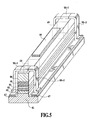
- Fig. 5 is a perspective view for explaining a seventh example of the semiconductor optoelectronic waveguide.
- the symbol 41 given in the figure denotes an n-type third semiconductor clad layer; 42, a p-type fifth semiconductor clad layer arranged on the third semiconductor clad layer 41; 43, a first semiconductor clad layer arranged on the fifth semiconductor clad layer 42; 44, a semiconductor core layer arranged on the first semiconductor clad layer 43 and having electro-optical effects; 45, a second semiconductor clad layer arranged on the semiconductor core layer 44; 46, an n-type fourth semiconductor clad layer arranged on the second semiconductor clad layer 45; 47 and 48, n-type electrodes; 49, an electrical isolation region formed by ion implantation; 50-1, an electrode formed in an n-type fourth semiconductor clad layer; 50-2, an electric wiring in which an electrode formed in the n-type fourth semiconductor clad layer is made at the same potential with the third clad layer. It is noted that
- the n-type electrode 50-1 is formed on the fourth semiconductor clad layer 46 at the portion that is opposed to an optical modulation waveguide portion across the electrical isolation region 49, and connected by the electric wiring 50-2 , thereby making the potential the same as that of the third semiconductor clad layer 41.
- the electrical isolation region is not sufficiently high in resistance, the problem is removed that the potential outside the electrical isolation region 49 is elevated to result in application of bias voltage to portions other than a main waveguide portion.
- the present disclosure is effective in stably realizing features of an optical modulator using a nin-type heterostructure which can be driven at a low voltage and able to contribute to a smaller electric power consumption of an optical modulator module and a lower manufacturing cost of the module through reduction in input optical power.
- InP and InAlGaAs are exemplified as semiconductor materials for a semiconductor optoelectronic waveguide.
- the present invention is not restricted thereto but also applicable to an optoelectronic waveguide structure in which other family of III-V compound semiconductors including AlGaAs and InGaAsP compounds are used.
- an n-type is given to clad layers on both sides of the InP/InGaAsP optical modulator (a so-called nin-type structure).
- a semiconductor clad layer 22 into which a p-type doping layer is introduced is inserted below the core layer 24 as the barrier layer.
- Both sides of an n-type clad layer 26 above the core layer 24 are given a p-type layer which is used as an electrical separation layer 29.
- the symbol 21 denotes an n-type third semiconductor clad layer; 23, a first semiconductor clad layer; 25, a second semiconductor clad layer; 29-1, a connection waveguide region of the fourth semiconductor clad layers 26 and 29; 27 and 28, electrodes.
- a waveguide structure of the nin-type InP/InGaAsP optical modulator illustrated in Fig. 3 has excellent features that the modulator can be driven at a low voltage.
- a phenomenon parasitsitic phototransistor effect
- the core layer 24 has a light absorption although in a sparing quantity, holes generated therein accumulate on the barrier layer 22, thereby resulting in reduction in barrier height to electrons to generate leak current.
- This is another problem to be solved. More specifically, with reference to transistor operation, when base-hole concentrations are elevated, with a base kept open, an emitter/base junction is kept in a forward bias state. Further, voltage applied to the core layer 24 is lowered only by voltage of the forward bias, resulting in a change in modulation characteristics by light wavelength and light intensity, thereby restricting the applications as a modulator.
- Fig. 6 is a perspective view for explaining an eighth example of the semiconductor optoelectronic waveguide according to the present invention.
- the symbol 61 given in the figure denotes a third semiconductor clad layer; 62, a first semiconductor clad layer arranged on the third semiconductor clad layer 61; 63, a semiconductor core layer arranged on the first semiconductor clad layer 62; 64, a second semiconductor clad layer arranged on the semiconductor core layer 63; 65, a fifth semiconductor clad layer arranged on the second semiconductor clad layer 64; 66, a fourth semiconductor clad layer arranged on the fifth semiconductor clad layer 65; 66-1, an optical modulation region; 66-2, an isolation region; 66-3, a connection waveguide region; 67 and 68, electrodes.
- the third semiconductor clad layer 61 is an n-type third InP clad layer
- the first semiconductor clad layer 62 is a first InGaAlAs clad layer whose band gap is smaller than that of InP at lower doping concentrations.
- the material and dimension of the semiconductor core layer 63 is determined in such a way that electro-optical effects are effectively exerted at an operating light wavelength and light absorption is kept lower not to pose any problem.
- a quantum well layer and a barrier layer each of which is changed in Ga/Al compositions of InGaAlAs, are used to forma multiple quantum well structure.
- the second semiconductor clad layer 64 is a second InGaAlAs clad layer whose band gap is smaller than that of InP at low doping concentrations and in which a p-type InP barrier layer 65 (fifth semiconductor clad layer) is arranged on the clad layer 64.
- the fourth InP clad layer 66 is constituted with three regions.
- the optical modulation region 66-1 is constituted with an n-type InP layer and the isolation region 66-2 is a p-type InP region, whose bottom surface is in contact with the p-type InP barrier layer 65.
- the p-type InP region 66-2 is formed, for example, by removing a portion corresponding to the isolation region 66-2 by etching to grow again a p-type InP after growth of the third semiconductor clad layer 61 to the fourth semiconductor clad layer 66 or by introducing a Be acceptor into a part of the fourth semiconductor clad layer 66 through ion implantation.
- the connection waveguide region 66-3 is an InP formed irrespective of a conductive configuration.
- Electrodes 67 and 68 are metal electrodes, and voltage is applied to the core layer 63, with one electrode 68 being negative polarity to the other electrode 67.
- the metal electrode 68 is in electrical contact with both the optical modulation region 66-1 and the isolation region 66-2.
- the first semiconductor clad layer 62 just under the optical modulation region through the fifth semiconductor clad layer 65 are all determined with doping concentrations so that an n-type neutrality is substantially maintained, excluding a depleted portion which is a part of the interface between the n-type InP clad layer 66-1 and the p-type InP barrier layer 65.
- an electrical signal is input toanelectrode 68 toapplyvoltage between an n-type third InP clad layer 61 and an n-type InP optical modulation region 66-1.
- the InP barrier layer 65 is p-type and functions as a potential barrier to electrons, electron injection from the optical modulation region 66-1 is suppressed and voltage is applied to the core layer 63 in a state that leak current is generated less, thereby making it possible to modulate an optical phase on the basis of electro-optical effects.
- connection waveguide region 66-3 is arranged at an optical modulation regionwhere voltage is applied and on the light input/output side of the optical modulation region to provide an electrical separation between them.
- a portion indicated by the isolation region 66-2 in Fig. 6 is selectively given a p-type region (p-type InP region), which is used as an electrical isolation region.
- Introduction of the p-type InP region 66-2 electrically connected to the n-type InP clad layer 66-1 has the following actions. Namely, in the waveguide structure as illustrated in Fig. 3 , as described above, a parasitic phototransistor effect results in association with holes generated by light absorption of the core layer 24. However, in the structure of the present example, since the p-type InP region (isolation region) 66-2 is lower in potential than a depleted barrier layer 65, holes flow into the p-type InP region (isolation region) 66-2, thereby preventing accumulation of holes inside the barrier layer 65.
- Fig. 7 is a perspective view for explaining a ninth example of the semiconductor optoelectronic waveguide according to the present invention.
- the p-type InP region 66-2 is arranged on both sides of the optical modulation region 66-1.
- the waveguide is made longer, holes generated by light absorption do not effectively flow into the p-type InP region 66-2.
- many p-type InP regions 76-2 may be arranged inside the optical modulation region.
- these regions 76-2 are in electrical contact with the n-type InP region 76-1.
- the p-type InP region 76-2 is made shorter in a longitudinal direction, it is possible to suppress an increase in light absorption by introduction of the p-type layer to the least possible extent, while keeping the effect of hole absorption.
- an electrode 78 is connected to each of the p-type InP regions 76-2, giving the same potential to these regions 76-2. Therefore, these regions will not adversely affect transmission of an electrical signal.
- the symbol 71 denotes an n-type third semiconductor clad layer; 72, a first semiconductor clad layer arranged on the third semiconductor clad layer 71; 73, a semiconductor core layer arranged on the first semiconductor clad layer 72 and having electro-optical effects; 74, a second semiconductor clad layer arranged on the semiconductor core layer 73; 75, a p-type fifth semiconductor clad layer arranged on the second semiconductor clad layer 74; 76, a fourth semiconductor clad layer arranged on the fifth semiconductor clad layer 75; 76-3, a p-type region (isolation region) of the fourth semiconductor clad layer; 76-4, a connection waveguide region of the fourth semiconductor clad layer; 77, an n-type electrode.
- Fig. 8 is a perspective view for explaining a tenth example of the semiconductor optoelectronic waveguide according to the present invention.
- the symbol 81 given in the figure denotes an n-type third semiconductor clad layer; 82, a first semiconductor clad layer arranged on the third semiconductor clad layer 81; 83, a semiconductor core layer arranged on the first semiconductor clad layer 82 and having electro-optical effects; 84, a second semiconductor clad layer arranged on the semiconductor core layer 83; 85, a p-type fifth semiconductor clad layer arranged on the second semiconductor clad layer 84; 86, a fourth semiconductor clad layer arranged on the fifth semiconductor clad layer 85; 86-1, ann-type region (optical modulation region) of the fourth semiconductor clad layer; 86-2, a p-type region (isolation region) of the fourth semiconductor clad layer; 86-3, a connection waveguide region of the fourth semiconductor clad layer; 87 and
- the semiconductor optoelectronic waveguide of the tenth example is constituted in such a way that the electrode 89 is respectively formed on the fourth clad layer (connection waveguide portion) 86-3 which is opposed to the optical modulation region 86-1 across the p-type InP region 86-2 functioning as an electrical isolation region and the electric wiring 90 is connectedbetween the electrode 89 and the electrode 87 on the third semiconductor clad layer 81, by which the connection waveguide region 86-3 is made at the same potential with the third clad layer 81.
- connection waveguide region 86-2 is not sufficiently high in resistance, potential outside the electrical isolation region is elevated to result in application of bias voltage to portions other than major waveguide portions.
- a conductive configuration of the above-described connection waveguide region may be a p-type, an n-type or a depleted layer. In any case, no type will develop a state where a forward bias is given between the connection waveguide region and the optical modulation region so that electric current flows.
- the ninth example is combined with the tenth example in the present invention.
- InP and InAlGaAs are exemplified as materials.
- the present invention is also applicable to an optoelectronic waveguide structure in which other family of III-V compound semiconductors including AlGaAs and InGaAsP compounds are used. Therefore, the embodiments of the present invention are not restricted to those described above but include substitution of materials and others, change in configuration and number of components and a simple combination of known parts and disclosed technology, as long as they are in the range of the patent claims hereof.
- a method for integrating the semiconductor optoelectronic waveguide of the present disclosure with a semiconductor laser is, as a matter of course, technically the same with a known method for integrating an electric field absorption-type optical modulator with a semiconductor laser.
- the present disclosure relates to a semiconductor optoelectronic waveguide having an isolation structure for electrical signal line in an nin-type heterostructure optoelectronic waveguide, which is used in an ultrahigh-speed optical modulator at a long wavelength region. Further, the present disclosure is able to provide a semiconductor optoelectronic waveguide which can less influence the transmission of an optical mode than a conventional recess-formed electrical isolation region to solve a problem of optical loss and which has a structure of electrical isolation region which is well controllable and stable.
- the semiconductor optoelectronic waveguide of the present disclosure is applicable to an ultrahigh-speed optical modulator at a long wavelength region and expected to make a great contribution to high-speed optical network communications systems and the like.
Landscapes
- Physics & Mathematics (AREA)
- Nonlinear Science (AREA)
- Optics & Photonics (AREA)
- Chemical & Material Sciences (AREA)
- Engineering & Computer Science (AREA)
- Nanotechnology (AREA)
- General Physics & Mathematics (AREA)
- Life Sciences & Earth Sciences (AREA)
- Biophysics (AREA)
- Crystallography & Structural Chemistry (AREA)
- Optical Modulation, Optical Deflection, Nonlinear Optics, Optical Demodulation, Optical Logic Elements (AREA)
- Optical Integrated Circuits (AREA)
Claims (2)
- Guide d'ondes optoélectronique semi-conducteur de type moulure comportant une hétérostructure de type nin, le guide d'onde comportant:- une couche centrale semi-conducteur (63, 73, 83) ayant des effets électro-optiques;- une première et une deuxième couche de revêtement semi-conducteur (62, 72, 82/64, 74, 84) agencées au-dessous et au-dessus de la couche centrale semi-conducteur respectivement;- une troisième couche de revêtement semi-conducteur de type n (61, 71, 81) qui est agencée au-dessous de la première couche de revêtement semi-conducteur;- une quatrième couche de revêtement semi-conducteur (66, 76, 86) qui est agencée au-dessus de la deuxième couche de revêtement semi-conducteur, la quatrième couche de revêtement semi-conducteur comportant une zone majeure de type n (66-1, 76-1, 86-1) le long de la direction de moulure et une zone d'isolation de type p (66-2, 76-3, 86-2) adjacente à la zone majeure à l'intérieur de la quatrième couche de revêtement;- une cinquième couche de revêtement semi-conducteur de type p (65, 75, 85) agencée entre la deuxième couche der revêtement semi-conducteur et la quatrième couche de revêtement semi-conducteur;- une électrode supérieure (68, 78, 88) en contact avec ladite zone majeure et ladite zone d'isolation; et- une autre électrode (67, 77, 87) prévue sur la troisième couche de revêtement semi-conducteur,dans lequel
lesdites électrodes sont configurées pour appliquer une tension électrique à la couche centrale semi-conducteur; et
les bandes interdites de la première, deuxième et cinquième couche de revêtement semi-conducteur sont plus larges que la bande interdite de la couche centrale semi-conducteur. - Guide d'onde optoélectronique semi-conducteur selon la revendication 1, la quatrième couche de revêtement comportant une zone de guide d'onde de raccord (86-3) le long de la direction de la moulure et adjacente à la zone d'isolation de type p (86-2), dans lequel la zone majeure (86-1), la zone d'isolation de type p (86-2) et ladite zone de guide d'onde de raccord (86-3) sont agencées dans cet ordre et dans lequel une électrode (89) est formée sur ladite zone de guide d'onde de raccord, l'électrode (89) étant raccordée électriquement à l'électrode (87) prévue sur la troisième couche de revêtement semi-conducteur.
Applications Claiming Priority (3)
| Application Number | Priority Date | Filing Date | Title |
|---|---|---|---|
| JP2003346285A JP2005116644A (ja) | 2003-10-03 | 2003-10-03 | 半導体光電子導波路 |
| JP2003346287A JP4105618B2 (ja) | 2003-10-03 | 2003-10-03 | 半導体光変調導波路 |
| EP04792011A EP1672410A4 (fr) | 2003-10-03 | 2004-10-04 | Guide d'onde photoelectronique a semi-conducteurs |
Related Parent Applications (2)
| Application Number | Title | Priority Date | Filing Date |
|---|---|---|---|
| EP04792011.1 Division | 2004-10-04 | ||
| EP04792011A Division EP1672410A4 (fr) | 2003-10-03 | 2004-10-04 | Guide d'onde photoelectronique a semi-conducteurs |
Publications (3)
| Publication Number | Publication Date |
|---|---|
| EP2000848A2 EP2000848A2 (fr) | 2008-12-10 |
| EP2000848A3 EP2000848A3 (fr) | 2009-06-24 |
| EP2000848B1 true EP2000848B1 (fr) | 2012-12-12 |
Family
ID=34425355
Family Applications (2)
| Application Number | Title | Priority Date | Filing Date |
|---|---|---|---|
| EP08017012A Expired - Fee Related EP2000848B1 (fr) | 2003-10-03 | 2004-10-04 | Guide d'onde optoélectronique à semi-conducteur |
| EP04792011A Withdrawn EP1672410A4 (fr) | 2003-10-03 | 2004-10-04 | Guide d'onde photoelectronique a semi-conducteurs |
Family Applications After (1)
| Application Number | Title | Priority Date | Filing Date |
|---|---|---|---|
| EP04792011A Withdrawn EP1672410A4 (fr) | 2003-10-03 | 2004-10-04 | Guide d'onde photoelectronique a semi-conducteurs |
Country Status (3)
| Country | Link |
|---|---|
| US (2) | US7599595B2 (fr) |
| EP (2) | EP2000848B1 (fr) |
| WO (1) | WO2005033784A1 (fr) |
Families Citing this family (4)
| Publication number | Priority date | Publication date | Assignee | Title |
|---|---|---|---|---|
| JP4870518B2 (ja) * | 2006-10-24 | 2012-02-08 | Nttエレクトロニクス株式会社 | 半導体光変調器 |
| JP5265929B2 (ja) * | 2008-01-10 | 2013-08-14 | Nttエレクトロニクス株式会社 | 半導体光変調器及び光変調装置 |
| JP5831165B2 (ja) * | 2011-11-21 | 2015-12-09 | 富士通株式会社 | 半導体光素子 |
| CN111373312B (zh) * | 2017-11-30 | 2023-08-04 | 三菱电机株式会社 | 半导体光调制器 |
Family Cites Families (13)
| Publication number | Priority date | Publication date | Assignee | Title |
|---|---|---|---|---|
| US5008717A (en) * | 1989-03-03 | 1991-04-16 | At&T Bell Laboratories | Semiconductor device including cascaded modulation-doped quantum well heterostructures |
| JPH03231220A (ja) * | 1990-02-07 | 1991-10-15 | Nippon Telegr & Teleph Corp <Ntt> | 半導体光素子 |
| JPH0575212A (ja) | 1991-09-17 | 1993-03-26 | Nippon Telegr & Teleph Corp <Ntt> | 光非線形増幅素子 |
| JPH05307200A (ja) * | 1992-04-30 | 1993-11-19 | Nippon Telegr & Teleph Corp <Ntt> | 導波路型光スイッチ及びその製造方法 |
| JPH0750403A (ja) * | 1993-08-04 | 1995-02-21 | Nippon Telegr & Teleph Corp <Ntt> | 光マトリックススイッチ |
| US5684818A (en) * | 1993-12-28 | 1997-11-04 | Fujitsu Limited | Stepped substrate semiconductor laser for emitting light at slant portion |
| JPH08335745A (ja) * | 1995-06-07 | 1996-12-17 | Fujitsu Ltd | 半導体発光装置 |
| US5647029A (en) | 1995-11-27 | 1997-07-08 | Lucent Technologies Inc. | Traveling wave quantum well waveguide modulators using velocity matching for improved frequency performance |
| US6198853B1 (en) | 1997-10-31 | 2001-03-06 | Oki Electric Industry Co., Ltd. | Semiconductor optical functional element |
| JP3897420B2 (ja) * | 1997-10-31 | 2007-03-22 | 沖電気工業株式会社 | 半導体光変調装置およびその製造方法 |
| JP3839710B2 (ja) | 2001-12-11 | 2006-11-01 | 富士通株式会社 | 半導体光変調器、マッハツェンダ型光変調器、及び光変調器一体型半導体レーザ |
| JP2003241152A (ja) | 2002-02-18 | 2003-08-27 | Mitsubishi Electric Corp | 半導体光変調器 |
| JP2007516607A (ja) * | 2003-05-29 | 2007-06-21 | アプライド マテリアルズ インコーポレイテッド | 埋込式導波路検出器 |
-
2004
- 2004-10-04 US US10/574,513 patent/US7599595B2/en not_active Expired - Fee Related
- 2004-10-04 EP EP08017012A patent/EP2000848B1/fr not_active Expired - Fee Related
- 2004-10-04 EP EP04792011A patent/EP1672410A4/fr not_active Withdrawn
- 2004-10-04 WO PCT/JP2004/014600 patent/WO2005033784A1/fr active Application Filing
-
2008
- 2008-07-15 US US12/219,061 patent/US7787736B2/en not_active Expired - Fee Related
Also Published As
| Publication number | Publication date |
|---|---|
| US7787736B2 (en) | 2010-08-31 |
| EP1672410A8 (fr) | 2006-11-22 |
| US20080304786A1 (en) | 2008-12-11 |
| EP1672410A1 (fr) | 2006-06-21 |
| EP2000848A3 (fr) | 2009-06-24 |
| US7599595B2 (en) | 2009-10-06 |
| EP2000848A2 (fr) | 2008-12-10 |
| US20070172184A1 (en) | 2007-07-26 |
| WO2005033784A1 (fr) | 2005-04-14 |
| EP1672410A4 (fr) | 2008-02-20 |
Similar Documents
| Publication | Publication Date | Title |
|---|---|---|
| EP2317371B1 (fr) | Modulateur optique à semiconducteur | |
| US5680411A (en) | Integrated monolithic laser-modulator component with multiple quantum well structure | |
| EP2081075B1 (fr) | Modulateur optique à semi-conducteur utilisant une structure npin | |
| US5165105A (en) | Separate confinement electroabsorption modulator utilizing the Franz-Keldysh effect | |
| JP5170236B2 (ja) | 導波路型半導体光変調器及びその製造方法 | |
| EP2230549B1 (fr) | Modulateur de lumière à semi-conducteur et dispositif de modulation de lumière | |
| JP4047785B2 (ja) | 半導体光電子導波路 | |
| JP5801589B2 (ja) | 光変調素子 | |
| US7787736B2 (en) | Semiconductor optoelectronic waveguide | |
| JP2011029595A (ja) | 光モジュール及び集積型半導体光素子及びその製造方法 | |
| JP2005116644A (ja) | 半導体光電子導波路 | |
| US6897993B2 (en) | Electroabsorption modulator, modulator laser device and method for producing an electroabsorption modulator | |
| JP4105618B2 (ja) | 半導体光変調導波路 | |
| US20210184421A1 (en) | Semiconductor Optical Element | |
| Knodl et al. | Integrated 1.3-µm InGaAlAs-InP laser-modulator with double-stack MQW layer structure | |
| JP6151958B2 (ja) | 光変調素子および光変調素子の駆動方法 | |
| US20240006844A1 (en) | Semiconductor Optical Device | |
| EP1849037B1 (fr) | Modulateur optique | |
| Hasebe et al. | 50-Gbit/s operation of lateral pin diode structure electro-absorption modulator integrated DFB laser | |
| JP4283079B2 (ja) | 半導体光電子導波路 | |
| Chen et al. | Two stacks of MQW for fabricating high-speed electro-absorption modulator integrated DFB laser | |
| Tamura et al. | Ultrafast electroabsorption modulators with traveling-wave electrodes | |
| JPH02170118A (ja) | 半導体光スイッチ |
Legal Events
| Date | Code | Title | Description |
|---|---|---|---|
| PUAI | Public reference made under article 153(3) epc to a published international application that has entered the european phase |
Free format text: ORIGINAL CODE: 0009012 |
|
| 17P | Request for examination filed |
Effective date: 20080926 |
|
| AC | Divisional application: reference to earlier application |
Ref document number: 1672410 Country of ref document: EP Kind code of ref document: P |
|
| AK | Designated contracting states |
Kind code of ref document: A2 Designated state(s): DE FR GB SE |
|
| PUAL | Search report despatched |
Free format text: ORIGINAL CODE: 0009013 |
|
| AK | Designated contracting states |
Kind code of ref document: A3 Designated state(s): DE FR GB SE |
|
| RIC1 | Information provided on ipc code assigned before grant |
Ipc: G02F 1/025 20060101AFI20081030BHEP Ipc: G02F 1/017 20060101ALI20090520BHEP |
|
| 17Q | First examination report despatched |
Effective date: 20090731 |
|
| AKX | Designation fees paid |
Designated state(s): DE FR GB SE |
|
| GRAP | Despatch of communication of intention to grant a patent |
Free format text: ORIGINAL CODE: EPIDOSNIGR1 |
|
| GRAS | Grant fee paid |
Free format text: ORIGINAL CODE: EPIDOSNIGR3 |
|
| GRAA | (expected) grant |
Free format text: ORIGINAL CODE: 0009210 |
|
| RAP1 | Party data changed (applicant data changed or rights of an application transferred) |
Owner name: NIPPON TELEGRAPH AND TELEPHONE CORPORATION Owner name: NTT ELECTRONICS CORPORATION |
|
| AC | Divisional application: reference to earlier application |
Ref document number: 1672410 Country of ref document: EP Kind code of ref document: P |
|
| AK | Designated contracting states |
Kind code of ref document: B1 Designated state(s): DE FR GB SE |
|
| REG | Reference to a national code |
Ref country code: GB Ref legal event code: FG4D |
|
| REG | Reference to a national code |
Ref country code: DE Ref legal event code: R096 Ref document number: 602004040417 Country of ref document: DE Effective date: 20130207 |
|
| PG25 | Lapsed in a contracting state [announced via postgrant information from national office to epo] |
Ref country code: SE Free format text: LAPSE BECAUSE OF FAILURE TO SUBMIT A TRANSLATION OF THE DESCRIPTION OR TO PAY THE FEE WITHIN THE PRESCRIBED TIME-LIMIT Effective date: 20121212 |
|
| PLBE | No opposition filed within time limit |
Free format text: ORIGINAL CODE: 0009261 |
|
| STAA | Information on the status of an ep patent application or granted ep patent |
Free format text: STATUS: NO OPPOSITION FILED WITHIN TIME LIMIT |
|
| 26N | No opposition filed |
Effective date: 20130913 |
|
| REG | Reference to a national code |
Ref country code: DE Ref legal event code: R097 Ref document number: 602004040417 Country of ref document: DE Effective date: 20130913 |
|
| GBPC | Gb: european patent ceased through non-payment of renewal fee |
Effective date: 20131004 |
|
| REG | Reference to a national code |
Ref country code: DE Ref legal event code: R119 Ref document number: 602004040417 Country of ref document: DE Effective date: 20140501 |
|
| PG25 | Lapsed in a contracting state [announced via postgrant information from national office to epo] |
Ref country code: GB Free format text: LAPSE BECAUSE OF NON-PAYMENT OF DUE FEES Effective date: 20131004 |
|
| REG | Reference to a national code |
Ref country code: FR Ref legal event code: ST Effective date: 20140630 |
|
| PG25 | Lapsed in a contracting state [announced via postgrant information from national office to epo] |
Ref country code: FR Free format text: LAPSE BECAUSE OF NON-PAYMENT OF DUE FEES Effective date: 20131031 Ref country code: DE Free format text: LAPSE BECAUSE OF NON-PAYMENT OF DUE FEES Effective date: 20140501 |