EP2000835A1 - Structure de propagation d'ondes électromagnétiques - Google Patents
Structure de propagation d'ondes électromagnétiques Download PDFInfo
- Publication number
- EP2000835A1 EP2000835A1 EP08251051A EP08251051A EP2000835A1 EP 2000835 A1 EP2000835 A1 EP 2000835A1 EP 08251051 A EP08251051 A EP 08251051A EP 08251051 A EP08251051 A EP 08251051A EP 2000835 A1 EP2000835 A1 EP 2000835A1
- Authority
- EP
- European Patent Office
- Prior art keywords
- wave
- electromagnetic wave
- propagating
- main body
- wavelength
- Prior art date
- Legal status (The legal status is an assumption and is not a legal conclusion. Google has not performed a legal analysis and makes no representation as to the accuracy of the status listed.)
- Granted
Links
Images






Classifications
-
- G—PHYSICS
- G02—OPTICS
- G02B—OPTICAL ELEMENTS, SYSTEMS OR APPARATUS
- G02B6/00—Light guides; Structural details of arrangements comprising light guides and other optical elements, e.g. couplings
- G02B6/10—Light guides; Structural details of arrangements comprising light guides and other optical elements, e.g. couplings of the optical waveguide type
- G02B6/12—Light guides; Structural details of arrangements comprising light guides and other optical elements, e.g. couplings of the optical waveguide type of the integrated circuit kind
-
- G—PHYSICS
- G02—OPTICS
- G02B—OPTICAL ELEMENTS, SYSTEMS OR APPARATUS
- G02B6/00—Light guides; Structural details of arrangements comprising light guides and other optical elements, e.g. couplings
- G02B6/10—Light guides; Structural details of arrangements comprising light guides and other optical elements, e.g. couplings of the optical waveguide type
- G02B6/12—Light guides; Structural details of arrangements comprising light guides and other optical elements, e.g. couplings of the optical waveguide type of the integrated circuit kind
- G02B6/122—Basic optical elements, e.g. light-guiding paths
- G02B6/1226—Basic optical elements, e.g. light-guiding paths involving surface plasmon interaction
-
- B—PERFORMING OPERATIONS; TRANSPORTING
- B82—NANOTECHNOLOGY
- B82Y—SPECIFIC USES OR APPLICATIONS OF NANOSTRUCTURES; MEASUREMENT OR ANALYSIS OF NANOSTRUCTURES; MANUFACTURE OR TREATMENT OF NANOSTRUCTURES
- B82Y20/00—Nanooptics, e.g. quantum optics or photonic crystals
-
- G—PHYSICS
- G02—OPTICS
- G02B—OPTICAL ELEMENTS, SYSTEMS OR APPARATUS
- G02B26/00—Optical devices or arrangements for the control of light using movable or deformable optical elements
- G02B26/08—Optical devices or arrangements for the control of light using movable or deformable optical elements for controlling the direction of light
- G02B26/10—Scanning systems
-
- G—PHYSICS
- G02—OPTICS
- G02B—OPTICAL ELEMENTS, SYSTEMS OR APPARATUS
- G02B5/00—Optical elements other than lenses
- G02B5/008—Surface plasmon devices
-
- G—PHYSICS
- G02—OPTICS
- G02B—OPTICAL ELEMENTS, SYSTEMS OR APPARATUS
- G02B6/00—Light guides; Structural details of arrangements comprising light guides and other optical elements, e.g. couplings
Definitions
- the invention relates to an electromagnetic wave propagating structure, more particularly to an electromagnetic wave propagating structure that surpasses diffraction limit and that enhances resolution and precision of optical systems which incorporate the electromagnetic wave propagating structure.
- Electromagnetic wave technology is one of the most widely used basic technologies in high-technological industries such as medical examination, precision measurement, semiconductor industry, etc. Therefore, the search for ways to enhance the resolution and precision of optical technology is what both the academic and industrial communities are striving for.
- the behavior of light is limited by the diffraction limit, which restricts the minimum value of the product of angular divergence (sine of diffraction angle (sin ⁇ ) ) and a width of light beam (2w).
- the achievable highest resolution for a focused light spot in optical systems is approximately 0.61 times the wavelength of the incident light beam (half of the wavelength in 1-D).
- an object of the present invention is to provide an electromagnetic wave propagating structure that is capable of enhancing resolution and precision in optical systems.
- an electromagnetic wave propagating structure adapted for use in an electromagnetic wave propagating system.
- the electromagnetic wave propagating system includes a wave emanating block, from which an electromagnetic wave having a wavelength is adapted to propagate in a wave-propagating direction, and a wave receiving block.
- the electromagnetic wave propagating structure includes a main body that has surfaces capable of blocking propagation of the electromagnetic wave, and that includes an incident side and an exit side opposite to the incident side in the wave-propagating direction.
- the main body is formed with two wave-propagating channels that are spaced apart from each other by a distance not greater than the wavelength of the electromagnetic wave.
- Each of the wave-propagating channels extends from the incident side to the exit side and has an inner dimension not greater than half of the wavelength of the electromagnetic wave.
- the electromagnetic wave propagating structure is adapted to allow an electromagnetic wave to propagate from the wave emanating block therethrough via the wave-propagating channels toward the wave receiving block for focusing into a light spot having a spot size that is smaller than half of the wavelength of the electromagnetic wave.
- Another object of the present invention is to provide an electromagnetic wave propagating structure suitable for producing a super collimated beam.
- an electromagnetic wave propagating structure adapted for use in an electromagnetic wave propagating system.
- the electromagnetic wave propagating system includes a wave emanating block, from which an electromagnetic wave having a wavelength is adapted to propagate in a wave-propagating direction.
- the electromagnetic wave propagating structure includes a main body that has surfaces capable of blocking propagation of the electromagnetic wave, and that includes an incident side and an exit side opposite to the incident side in a wave-propagating direction.
- the main body is formed with two wave-propagating channels that are spaced apart from each other by a distance not greater than the wavelength of the electromagnetic wave.
- Each of the wave-propagating channels extends from the incident side to the exit side and has an inner dimension not greater than half of the wavelength of the electromagnetic wave.
- the main body defines a central axis in the wave-propagating direction.
- Each of the wave-propagating channels has an incident opening at the incident side of the main body, an exit opening at the exit side of the main body, and an inner portion that extends between the incident and exit openings, that defines a central line parallel to the central axis and that has an inner dimension not greater than that of the exit opening.
- the inner portions of the wave-propagating channels are symmetrical about the central axis.
- the exit opening of each of the wave-propagating channels is symmetrical about the central line of the corresponding one of the wave-propagating channels.
- the main body is further formed with a plurality of periodically disposed grooves in the exit side. Each of the grooves has an inner dimension not greater than half of the wavelength of the electromagnetic wave. Adjacent ones of the grooves are spaced apart from each other by a distance not greater than the wavelength of the electromagnetic wave.
- At least one of the inner dimension and depth of each of the grooves and the distance between adjacent ones of the grooves is set such that the electromagnetic wave propagating structure is adapted to allow an electromagnetic wave to propagate from the wave emanating block therethrough via the wave-propagating channels for superimposing near the central axis and for continuing to propagate as a super collimated beam.
- the first preferred embodiment of an electromagnetic wave propagating structure according to the present invention is adapted to allow propagation of an electromagnetic wave therethrough. Due to the universality of the Maxwell equations, the electromagnetic wave propagating structure of the present invention is universally adaptable for electromagnetic waves having various wavelengths and frequencies, which include visible light, non-visible light, etc.
- the electromagnetic wave propagating structure includes a main body 1 formed with two wave-propagating channels 2 that are adapted to change propagating direction and energy distribution of an electromagnetic wave once the electromagnetic wave propagates therethrough.
- the main body 1 has surfaces capable of blocking propagation of the electromagnetic wave, and includes an incident side 11 and an exit side 12 opposite to the incident side 11 in a wave-propagating direction (y).
- the two wave-propagating channels 2 are formed spacedly in the main body 1 therethrough.
- Each of the wave-propagating channels 2 extends from the incident side 11 to the exit side 12, and has an incident opening 21 at the incident side 11, an exit opening 22 at the exit side 12, and an inner portion 23 extending between the incident opening 21 and the exit opening 22.
- the inner portion 23 of each of the wave-propagating channels 2 has an inner dimension that is not larger than half of a wavelength ( ⁇ ) of the electromagnetic wave that is to be propagated therethrough.
- the distance between the two wave-propagating channels 2 is not larger than the wavelength ( ⁇ ) of the electromagnetic wave that is to be propagated therethrough.
- each of the wave-propagating channels 2 is defined by a channel surface made from a material that enhances transmission of electromagnetic waves.
- the channel surfaces of the wave-propagating channels 2 are metallic.
- the effects achieved by the electromagnetic wave propagating structure were verified through simulations using the finite-difference time-domain (FDTD) method.
- the main body 1 which is made from a dispersive material such as a silver film or other materials that react strongly to electromagnetic waves, was modeled by the auxiliary difference equation method with Drude poles (which is the representation of the media of Drude model). Further, phasor polarized current was calculated in the simulations.
- the relationship between the electromagnetic wave propagating structure of the present invention and the behavior of the electromagnetic wave to be propagated through the electromagnetic wave propagating structure was verified by the simulation results that will be presented hereinbelow. Furthermore, the resultant focused light spot serves to verify the effects achieved by the electromagnetic wave propagating structure of the present invention.
- the simulation system is 2-dimensional, and is represented by a grid system having 600x600 cells of Yee space lattice with a unit cell length of 4nm.
- Each cell of the grid system is represented by an index (I x , I y ), where (I x ) and (I y ) respectively correspond to cell location in the first direction (x) and the wave-propagating direction (y) that are orthogonal to each other.
- the wave-propagating direction (y) is also referred interchangeably as the second direction (y) in this disclosure.
- (I x ) and (I y ) both have values that range from 1 to 600.
- the simulation system is also represented by a coordinate system that corresponds to the real dimensions of the grid system, which is 2.4 ⁇ m by 2.4 ⁇ m.
- the inner dimension (w1) of the inner portion 23 of each of the wave-propagating channels 2 is 80nm (i. e.
- channel width in°the first direction (x) is 80nm
- distance (d1) in the first direction (x) between the two wave-propagating channels 2 is 240nm.
- the electric field and the magnetic field are polarized respectively in the first direction (x) and a third direction (z) orthogonal to both the first direction (x) and the second direction (y), and are normalized as unity.
- Both boundaries for the first direction (x) of the simulation system at the non-negative portion in the second direction (y) of the coordinate system are set to be periodic in order to minimize numerical reflection and errors, while all other boundaries are set as Perfectly Matched Layer Absorbing Boundary Conditions.
- the time is normalized to the period of the electromagnetic wave, and the time step (dt) in the simulation is 0.004.
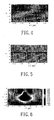
- the magnetic fields in the third direction (z), also referred to as the z-direction magnetic fields (H z ), exiting the two wave-propagating channels 2 overlap at a central portion corresponding to a central axis of the main body 1, i.e., corresponding to (C x ) of approximately 0.
- the electric fields in the wave-propagating direction (y), also referred to as the y-direction electric fields (Ey) exiting the two wave-propagating channels 2 cancel out at the central portion, and the energy thereof is converted into the z-direction magnetic field (H z ) and the electric field in the first direction (x), also referred to as the x-direction electric field (E x ).
- This phenomenon is one of the sub-wavelength antenna effects.
- the excitation of the surface currents and electromagnetic wave at the incident side 11 of the main body 1 and the coupling of the electromagnetic wave with the two wave-propagating channels 2 result in surface plasma movement and surface plasmon.
- the electromagnetic wave when traveling through each of the wave-propagating channels 2, polarizes surfaces defining the inner portion 23 of the corresponding one of the channels 2 such that the resultant polarized charges and current flow downward along with the electromagnetic wave toward the exit side 12 of the main body 1.
- the flowing polarized charges and current produce additional magnetic field in the third direction (z), i.e., (H z ), as a result of the sub-wavelength antenna effects.
- the z-direction magnetic field (H z ) is focused downwardly of the exit side 12 with the main body 1 as the reference, at which time the amplitude of the z-direction magnetic field (H z ) is 0.757.
- the propagation and focusing of the electromagnetic wave can also be verified by Poynting vectors (S1, S2) of the electric field and the magnetic field.
- the x-direction Poynting vector (S1) and the field energy flow toward the central portion of the main body 1.
- the y-direction Poynting vector (S2) and the field energy are focused downwardly of the exit side 12 of the main body 1 and continue to propagate downward and outward afterwards, indicating that the electromagnetic wave is a travelling electromagnetic wave.
- the present invention utilizing recent scientific advancements, surpasses the conventional wave theory, which indicates that the light cannot be transmitted through a sub-wavelength slit.
- the excitation of surface charge movement or a charge density wave on a metallic surface enhance the transmission of the electromagnetic wave.
- focusing of the electromagnetic wave into a light spot smaller than half of the wavelength of the electromagnetic wave is achieved by utilizing the sub-limit wave functions within the wave-propagating channels 2 of the innovative electromagnetic wave propagating structure.
- the wave function across the wave-propagating channels 2 is close to a constant and drops sharply on the surface of the main body 1.
- the second preferred embodiment of an electromagnetic wave propagating structure differs from the first preferred embodiment in that the main body 1a of the second preferred embodiment is further formed with at least one groove 13 at the exit side 12a.
- the groove 13 has an inner dimension that is not larger than half of the wavelength of the electromagnetic wave that is to be propagated through the wave-propagating channels 2, and is spaced apart from an adjacent one of the wave-propagating channels 2 by a distance not greater than the wavelength of the electromagnetic wave.
- a "pushing", “squeezing” or “compressing” phenomenon occurs in the focused light spot formed from the electromagnetic wave that propagates through the wave-propagating channels 2 of the second preferred embodiment such that the size of the focused light spot is diminished once again, and such that changes occur in the propagating direction and energy distribution of the electromagnetic wave downwardly of the exit side 12a of the main body 1a.
- the main body 1a is formed with one groove 13 for illustration purposes.
- the groove 13 has a groove depth (t2) in the wave-propagating direction (y) and a groove width (w2) in the first direction (x); both set to be 80nm.
- the distance (d2) between the right-hand one of the wave-propagating channels 2 and the groove 13 in the first direction (x) is set to be 120nm.
- the z-direction magnetic field (Hz) is focused downwardly of the exit side 12a into a light spot that has an energy averaged spot size of 0.328 ⁇ (a FWHM spot size of 0.378 ⁇ ) and an amplitude of 0.791, and that is smaller than half of the wavelength of the electromagnetic wave.
- the light spot is asymmetrical due to the "squeezed" or "compressed” phenomenon.
- the third preferred embodiment of an electromagnetic wave propagating structure according to the present invention differs from the second preferred embodiment in that the main body 1b of the third preferred embodiment is further formed with two of the grooves 13 at the exit side 12b.
- the grooves 13 are symmetrically disposed about a central axis of the main body 1b, and are disposed to interpose the wave-propagating channels 2 therebetween.
- the grooves 13 serve to squeeze the focused light spot.
- the electromagnetic wave is focused into a light spot having a size smaller than half of the wavelength of the electromagnetic wave.
- the fourth preferred embodiment of an electromagnetic wave propagating structure according to the present invention differs from the third preferred embodiment in that the main body 1c of the fourth preferred embodiment is further formed with a plurality of the grooves 13 at the exit side 12c.
- the grooves 13 are periodically spaced apart from each other, and the distance between each adjacent pair of the grooves 13 is not larger than the wavelength of the electromagnetic wave.
- the electromagnetic wave is focused into a light spot having a size smaller than half of the wavelength of the electromagnetic wave.
- the incident side 11 is formed with at least one groove
- the physical behavior of the electromagnetic wave coupling into and after propagating through the wave-propagating channels 2. will change. An example is provided hereinbelow.
- the fifth preferred embodiment of an electromagnetic wave propagating structure according to the present invention differs from the first preferred embodiment in that the main body 1d of the fifth preferred embodiment is further formed with a plurality of periodically spaced apart grooves 13 at the incident side 11d.
- Each of the grooves 13 has an inner dimension that is not larger than half of the wavelength of the electromagnetic wave.
- the distance between each adjacent pair of the grooves 13 is not larger than the wavelength of the electromagnetic wave.
- two of the grooves 13 are respectively disposed in spatial communication with the wave-propagating channels 2d such that the incident opening 21d of each of the wave-propagating channels 2d at the incident side 11d has an inner dimension not smaller than that of the inner portion 23 of each of the wave-propagating channels 2d between the incident opening 21d and the exit opening 22.
- the fifth preferred embodiment also results in focusing of the electromagnetic wave into a light spot having a size smaller than half of the wavelength of the electromagnetic wave.
- the electromagnetic wave propagating structure of the preferred embodiments disclosed hereinabove can also involve the use of a dielectric material.
- the fifth preferred embodiment of an electromagnetic wave propagating structure according to the present invention differs from the first preferred embodiment in the inclusion of a light-transmissible dielectric layer 3 disposed on the incident side 11 of the main body 1 for supporting the main body 1, for generating a waveguide effect, and for changing the propagating behavior of the electromagnetic wave that is to be propagated through the electromagnetic wave propagating structure.
- the light-transmissible dielectric layer 3 is made from glass.
- the sixth preferred embodiment also achieves the effect of focusing of the electromagnetic wave into a light spot having a size smaller than half of the wavelength of the electromagnetic wave.
- the seventh preferred embodiment of an electromagnetic wave propagating structure differs from the first preferred embodiment in that the exit opening 22e of each of the wave-propagating channels 2e is shaped asymmetrically about the central line of the inner portion 23 of the corresponding one of the wave-propagating channels 2e.
- the effect is that bending of the electromagnetic wave occurs after exiting the two wave-propagating channels 2e via the exit openings 22e, in which the electromagnetic wave, while maintaining a substantially unchanged energy distribution near the central axis of the main body 1e, continues to propagate downwardly away from the exit side 12e of the main body 1e toward the central axis of the main body 1e and is eventually focused into a light spot.
- the z-direction magnetic field (H z ) is focused into a light spot (with an amplitude of 1.30) having an energy averaged size of 0.341 ⁇ (or a FWHM spot size of 0.364 ⁇ ), which is smaller than half of the wavelength of the electromagnetic wave.
- the eighth preferred embodiment of an electromagnetic wave propagating structure according to the present invention differs from the seventh preferred embodiment in that the exit openings 22f of the two wave-propagating channels 2f are disposed in direct spatial communication with each other in the first direction (x).
- the eighth preferred embodiment also achieves a focused spot size of smaller than half of the wavelength of the electromagnetic wave, and that the electromagnetic wave bends after exiting the two wave-propagating channels 2f via the exit openings 22f prior to focusing into the light spot. Furthermore, after propagating toward the central axis of the main body 1f and being focused into the light spot, the electromagnetic wave continues to propagate with a high intensity.
- the ninth preferred embodiment of an electromagnetic wave propagating structure according to the present invention differs from the eighth preferred embodiment in that the main body 1g is further formed with a groove 13 on the exit side 12g.
- the groove 13 has an inner dimension not greater than half of the wavelength of the electromagnetic wave.
- the ninth preferred embodiment was verified to achieve the effect of focusing of the electromagnetic wave into a light spot having a size smaller than half of the wavelength of the electromagneticwave.
- the light spot is asymmetrical due to the "squeezed" or “compressed” phenomenon.
- the tenth preferred embodiment of an electromagnetic wave propagating structure according to the present invention differs from the ninth preferred embodiment in that the main body 1h of the tenth preferred embodiment is formed with two of the grooves 13 at the exit side 12h.
- the grooves 13 are symmetrically disposed about a central axis of the main body 1h, and are disposed to interpose the wave-propagating channels 2f therebetween.
- the grooves 13 serve to compress the focused light spot.
- the tenth preferred embodiment also achieves the effect of focusing of the electromagnetic wave into a light spot having a size smaller than half of the wavelength of the electromagnetic wave.
- the eleventh preferred embodiment of an electromagnetic wave propagating structure according to the present invention differs from the eighth preferred embodiment in that the main body li of the eleventh preferred embodiment is formed with a plurality of the grooves 13 at the exit side 12i.
- the grooves 13 are periodically spaced apart from each other, and the distance between each adjacent pair of the grooves 13 is not larger than the wavelength of the electromagnetic wave.
- the eleventh preferred embodiment similarly achieves the effect of focusing of the electromagnetic wave into a light spot having a size smaller than half of the wavelength of the electromagnetic wave.
- the incident side is formed with at least one groove
- the physical behavior of the electromagnetic wave coupling into and after propagating through the wave-propagating channels will change.
- An example is provided hereinbelow.
- the twelfth preferred embodiment of an electromagnetic wave propagating structure according to the present invention differs from the eighth preferred embodiment in that the main body 1j of the twelfth preferred embodiment is further formed with a plurality of periodically spaced apart grooves 13 at the incident side 11j .
- Each of the grooves 13 has an inner dimension that is not larger than half of the wavelength of the electromagnetic wave.
- the distance between each adjacent pair of the grooves 13 is not larger than the wavelength of the electromagnetic wave.
- the twelfth preferred embodiment was verified to achieve the effect of focusing of the electromagnetic wave into a light spot having a size smaller than half of the wavelength of the electromagnetic wave.
- the electromagnetic wave propagating structure of the seventh to twelfth preferred embodiments disclosed hereinabove can also involve the use of a dielectric material.
- the thirteenth preferred embodiment of an electromagnetic wave propagating structure according to the present invention differs from the eighth preferred embodiment in the inclusion of a light-transmissible dielectric layer 3 disposed on the incident side 11 of the main body 1f for supporting the main body 1f, for generating the waveguide effect, and for changing the propagating behavior of the electromagnetic wave that is to be propagated through the electromagnetic wave propagating structure.
- the light-transmissible dielectric layer 3 is made from glass. It was verified through simulation that the thirteenth preferred embodiment also achieves focusing of the electromagnetic wave into a light spot having a size smaller than half of the wavelength of the electromagnetic wave.
- the fourteenth preferred embodiment of an electromagnetic wave propagating structure according to the present invention differs from the first preferred embodiment in that the central lines of the wave-propagating channels 2p of the fourteenth preferred embodiment extend toward the central axis of the main body 1p from the incident side 11 toward the exit side 12 (i.e., the distance between each of the central lines and the central axis decreases gradually from the incident side 11 toward the exit side 12).
- the simulation system is also represented by a grid system having 600x600 cells of Yee space lattice with a unit cell length of 4nm.
- the main body 1p is set to have a thickness (t1 p ) in the wave-propagating direction (y) of 160nm (i.e., a distance between the incident side 11 and the exit side 12 of the main body 1p in the wave-propagating direction (y) is 160nm).
- the inner dimension (w1) of the inner portion 23 of each of the wave-propagating channels 2p is 80nm (i.e., channel width in the first direction (x) is 80nm).
- the distance (d1p) in the first direction (x) between the two wave-propagating channels 2p at the incident side 11 is 240nm
- the distance (d1p') in the first direction (x) between the two wave-propagating channels 2p at the exit side 12 is 200nm.
- Other simulation, parameters are identical to those disclosed hereinabove for the first preferred embodiment.
- the z-direction magnetic fields (H z ) are focused into a light spot (with an amplitude of 1.159) having an energy averaged size of 0.376 ⁇ (or a FWHM spot size of 0. 418 ⁇ ), which is smaller than half of the wavelength of the electromagnetic wave.
- the fifteenth preferred embodiment of an electromagnetic wave propagating structure according to the present invention differs from the fourteenth preferred embodiment in that the main body 1q of the fifteenth preferred embodiment is further formed with at least one groove 13 at the exit side 12q.
- the groove 13 has an inner dimension that is not larger than half of the wavelength of the electromagnetic wave that is to be propagated through the wave-propagating channels 2p, and is spaced apart from an adjacent one of the wave-propagating channels 2 by a distance not greater than the wavelength of the electromagnetic wave.
- the "pushing", “squeezing” or “compressing” phenomenon occurs in the focused light spot formed from the electromagnetic wave that propagates through the wave-propagating channels 2p of the fifteenth preferred embodiment such that the size of the focused light spot is diminished once again, and such that changes occur in the propagating direction and energy distribution of the electromagnetic wave downwardly of the exit side 12q of the main body 1q.
- the main body 1q is formed with one groove 13 for illustration purposes.
- the fifteenth preferred embodiment also achieves the effect of focusing of the electromagnetic wave into a light spot having a size smaller than half of the wavelength of the electromagnetic wave.
- the light spot is asymmetrical due to the "squeezed” or “compressed” phenomenon.
- the sixteenth preferred embodiment of an electromagnetic wave propagating structure according to the present invention differs from the fourteenth preferred embodiment in that the main body 1r of the sixteenth preferred embodiment is further formed with two of the grooves 13 at the exit side 12r.
- the grooves 13 are symmetrically disposed about a central axis of the main body 1r, and are disposed to interpose the wave-propagating channels 2p therebetween.
- the grooves 13 serve to squeeze the focused light spot.
- the seventeenth preferred embodiment of an electromagnetic wave propagating structure according to the present invention differs from the fourteenth preferred embodiment in that the main body 1s of the seventeenth preferred embodiment is further formed with a plurality of the grooves 13 at the exit side 12s.
- the grooves 13 are periodically spaced apart from each other, and the distance between each adjacent pair of the grooves 13 is not larger than the wavelength of the electromagnetic wave.
- the incident side is formed with at least one groove
- the physical behavior of the electromagnetic wave coupling into and after propagating through the wave-propagating channels will change.
- An example is provided hereinbelow.
- the eighteenth preferred embodiment of an electromagnetic wave propagating structure according to the present invention differs from the fourteenth preferred embodiment in that the main body 1t of the eighteenth preferred embodiment is further formed with a plurality of periodically spaced apart grooves 13 at the incident side 11t.
- Each of the grooves 13 has an inner dimension that is not larger than half of the wavelength of the electromagnetic wave.
- the distance between each adjacent pair of the grooves 13 is not larger than the wavelength of the electromagnetic wave.
- two of the grooves 13 are respectively disposed in spatial communication with the wave-propagating channels 2t such that the incident opening 21t of each of the wave-propagating channels 2t at the incident side 11t has an inner dimension not smaller than that of the inner portion 23t of each of the wave-propagating channels 2t between the incident opening 21t and the exit opening 22t.
- the eighteenth preferred embodiment also achieves the effect of focusing of the electromagnetic wave into a light spot having a size smaller than half of the wavelength of the electromagnetic wave.
- the electromagnetic wave propagating structure of the fourteenth to eighteenth preferred embodiments can also involve the use of a dielectric material.
- the nineteenth preferred embodiment of an electromagnetic wave propagating structure according to the present invention differs from the fourteenth preferred embodiment in the inclusion of a light-transmissible dielectric layer 3 disposed on the incident side 11 of the main body 1p for supporting the main body 1p, for generating a waveguide effect, and for changing the propagating behavior of the electromagnetic wave that is to be propagated through the electromagnetic wave propagating structure.
- the light-transmissible dielectric layer 3 is made from glass.
- the nineteenth preferred embodiment also achieves the effect of focusing of the electromagnetic wave into a light spot having a size smaller than half of the wavelength of the electromagnetic wave.
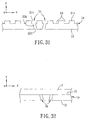
- the twentieth preferred embodiment of an electromagnetic wave propagating structure according to the present invention differs from the first preferred embodiment in that the main body 1u of the twentieth preferred embodiment is further formed with a plurality of periodically spaced apart grooves 13 at the exit side 12u.
- Each of the grooves 13 has an inner dimension that is not larger than half of the wavelength of the electromagnetic wave.
- the distance between each adjacent pair of the grooves 13 is not larger than the wavelength of the electromagnetic wave.
- two of the grooves 13 are respectively disposed in spatial communication with the wave-propagating channels 2u such that the exit opening 22u of each of the wave-propagating channels 2u has an inner dimension that is not smaller than that of the inner portion 23u of the corresponding one of the wave-propagating channels 2u.
- the inner portion 23u of each of the wave-propagating channels 2u has a central line that is parallel to the central axis of the main.body 1u. The central lines are equidistant from the central axis of the main body 1u in the first direction (x).
- the exit opening 22u of each of the wave-propagating channels 2u is symmetrical about the central line of the inner portion 23u of the corresponding one of the wave-propagating channels 2u.
- At least one of the inner dimension and depth of each of the grooves 13 and the distance between adjacent ones of the grooves 13 is set such that after the electromagnetic wave has propagated through the two wave-propagating channels 2u, the fields exiting the two wave-propagating channels 2u are superposed near the central axis of the main body 1u, and continue to propagate along the central axis while the energy distribution remains substantially unchanged during the propagation. In other words, a super-collimated beam is formed, where the angle of divergence is very close to zero.
- the simulation system has 3000x3000 cells of Yee space lattice with a unit cell length of 4nm.
- the electromagnetic wave has a wavelength of 633nm.
- each of the wave-propagating channels 2u is 40nm, and the distance (d1 u ) between the two wave-propagating channels 2u is 440nm.
- Each of the grooves 13 has a depth (t2 u ) of 80nm and a width (w2 u ) of 240nm.
- the distance (d3 u ) between each adjacent pair of the grooves 13 is 240nm.
- the electric field and magnetic field are polarized respectively in the first and third directions (x), (z), and are normalized as unity.
- Both boundaries for the first direction (x) of the simulation system at an upper portion of the main body 1u about a center of the main body 1u are periodic so as to minimize numerical reflection and errors, while all other boundaries are set as Perfectly Matched Layer Absorbing Boundary Conditions.
- the time is normalized to the period of the electromagnetic wave that is to be propagated through the wave propagating channels 2u, and the time step (dt) in the simulation is 0.004.
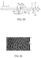
- the z-direction magnetic field (H z ) continues to propagate downwardly away from the exit side 12u of the main body 1u as a super-collimated beam with a substantially fixed amplitude for a distance larger than ten times the wavelength of the electromagnetic wave.
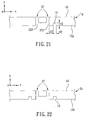
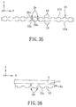
- the twenty-first preferred embodiment of an electromagnetic wave propagating structure according to the present invention differs from the twentieth preferred embodiment in that both the incident side 11v and the exit side 12u of the main body 1v are formed with the grooves 13 such that the inner dimensions of both of the incident and exit openings 21v, 22u of each of the wave-propagating channels 2v are not smaller than that of the inner portion 23u of the corresponding one of the wave-propagating channels 2v.
- the grooves 13 at the incident side 11v and the grooves 13 at the exit side 12u are symmetrically disposed about a longitudinal axis of the main body 1v in the first direction (x).
- the electromagnetic wave continues to propagate downwardly away from the exit side 12u of the main body 1v as a super-collimated beam with substantially fixed amplitude. Furthermore, the intensity of the electromagnetic wave after propagating through the wave-propagating channels 2v of the twenty-first preferred embodiment is greater than that after propagating through the wave-propagating channels 2u of the twentieth preferred embodiment.
- the electromagnetic wave propagating structure of the twentieth and twenty-first preferred embodiments can also involve the use of dielectric materials.
- the twenty-second preferred embodiment of an electromagnetic wave propagating structure according to the present invention further includes a light-transmissible dielectric layer 3 that is disposed on the incident side 11 of the main body 1u for supporting the main body 1u, for generating the waveguide effect, and for changing the propagating behavior of the electromagnetic wave that is to be propagated through the electromagnetic wave propagating structure.
- the light-transmissible dielectric layer is made from glass.
- effects similar to the twentieth preferred embodiment are achieved by the twenty-second preferred embodiment, where the electromagnetic wave continues to propagate downwardly away from the exit side 12u of the main body 1u while maintaining a fixed amplitude as a super-collimated beam after propagating through the main body 1u via the wave-propagating channels 2u.
- each of the wave-propagating channels 2 is factors that control the divergent angle and the diffraction behavior of the electromagnetic wave that propagates through the wave-propagating channels 2.
- the material composing the main body 1, and the presence of the dielectric layers 3 also take part in affecting the intensity variations of the electromagnetic wave during propagation through a system involving the electromagnetic wave propagating structure of the present invention. Therefore, all these factors can be adjusted and defined according to the requirements of a specific application so as to achieve the most desirable results.
- the electromagnetic wave propagating structure of this invention is suitable for application to an electromagnetic wave propagating system that includes a wave emanating block, from which an electromagnetic wave having a wavelength is adapted to propagate in a wave-propagating direction, and a wave receiving block.
- the electromagnetic wave propagating structure of the first through nineteenth preferred embodiments is provided between the wave emanating block and the wave receiving block, the electromagnetic wave that propagates from the wave emanating block through the electromagnetic wave propagating structure via the wave-propagating channels toward the wave receiving block is focused into a light spot having a spot size that is smaller than half of the wavelength of the electromagnetic wave.
- the electromagnetic wave propagating structure of the twentieth through twenty-second preferred embodiments is provided between the wave emanating block and the wave receiving block, the electromagnetic wave that propagates from the wave emanating block through the electromagnetic wave propagating structure via the wave-propagating channels continues to propagate toward the wave receiving block as a super-collimated beam.
- the electromagnetic wave propagating structure of the first through nineteenth preferred embodiments can be integrated with the wave emanating block to result in a light spot generator for focusing an electromagnetic wave into a light spot having a spot size that is smaller than half of the wavelength of the electromagnetic wave.
- the electromagnetic wave propagating structure of the twentieth through twenty-second preferred embodiments can be integrated with the wave emanating block to result in a light beam generator for generating a super-collimated beam from an electromagnetic wave.
- the electromagnetic wave propagating structure according to the present invention is suitable for various applications, such as in optical, semiconductor, and bio-tech industries.
- the application of the present invention in lithography processes results in finer, more delicate dots, lines and circuits.
- the present invention enhances the resolution and precision in optical systems, connects optical systems and electrical circuits, is applicable to sub-wavelength high resolution microscopes in biological and medical imaging industries, is applicable for more precise detection, changes and controls the structure, characteristics and dynamics of biological, chemical and physical systems, generates and reads smaller optical recording spots in optical storage industries, squeezes light into optical circuits having sizes smaller than the wavelength of the light, etc.
- the super-collimated beam provided by the present invention is suitable for applications requiring an electromagnetic wave beam without divergence during its propagation.
- the present invention allows the electromagnetic wave to diverge greatly after being focused, and thus is applicable where an increase of viewing angle is required, e.g., in light-emitting diodes.
- the subtraction and addition of the sub-wavelength optical fields are applicable in optical computation and control.
- the selectivity for various wavelengths of the electromagnetic wave allows application in filtering.
- the present invention successfully establishes an electromagnetic wave propagating structure that is adapted to generate a high intensity sub-wavelength focused spot after an electromagnetic wave propagates therethrough, and that has an exit structure that allows the electromagnetic wave to surpass the diffraction limit so as to diminish the size of the focused spot to thereby effectively enhance the resolution and precision of optical systems that incorporate the electromagnetic wave propagating structure of this invention.
- FDTD finite-difference time-domain
Landscapes
- Physics & Mathematics (AREA)
- Optics & Photonics (AREA)
- Engineering & Computer Science (AREA)
- General Physics & Mathematics (AREA)
- Nanotechnology (AREA)
- Chemical & Material Sciences (AREA)
- Microelectronics & Electronic Packaging (AREA)
- Life Sciences & Earth Sciences (AREA)
- Biophysics (AREA)
- Crystallography & Structural Chemistry (AREA)
- Investigating, Analyzing Materials By Fluorescence Or Luminescence (AREA)
- Exposure And Positioning Against Photoresist Photosensitive Materials (AREA)
- Exposure Of Semiconductors, Excluding Electron Or Ion Beam Exposure (AREA)
- Optical Integrated Circuits (AREA)
- Hall/Mr Elements (AREA)
Applications Claiming Priority (2)
| Application Number | Priority Date | Filing Date | Title |
|---|---|---|---|
| TW96120414 | 2007-06-06 | ||
| TW097103559A TWI372885B (en) | 2007-06-06 | 2008-01-30 | Electromagnetic wave propagating structure |
Publications (2)
| Publication Number | Publication Date |
|---|---|
| EP2000835A1 true EP2000835A1 (fr) | 2008-12-10 |
| EP2000835B1 EP2000835B1 (fr) | 2012-11-28 |
Family
ID=39676438
Family Applications (1)
| Application Number | Title | Priority Date | Filing Date |
|---|---|---|---|
| EP08251051A Not-in-force EP2000835B1 (fr) | 2007-06-06 | 2008-03-25 | Structure de propagation d'ondes électromagnétiques |
Country Status (6)
| Country | Link |
|---|---|
| US (2) | US8126305B2 (fr) |
| EP (1) | EP2000835B1 (fr) |
| JP (1) | JP4909307B2 (fr) |
| KR (1) | KR100934071B1 (fr) |
| SG (1) | SG148948A1 (fr) |
| TW (1) | TWI372885B (fr) |
Cited By (1)
| Publication number | Priority date | Publication date | Assignee | Title |
|---|---|---|---|---|
| KR100934071B1 (ko) * | 2007-06-06 | 2009-12-24 | 내셔날 쳉쿵 유니버시티 | 전자기파 전파 구조물, 전자기파 포커싱 방법, 콜리메이트광빔 생성 방법, 광 스폿 생성기 및 광빔 생성기 |
Families Citing this family (5)
| Publication number | Priority date | Publication date | Assignee | Title |
|---|---|---|---|---|
| US20120006981A1 (en) * | 2009-03-31 | 2012-01-12 | Imec | Waveguide integrated photodetector |
| US20120289832A1 (en) * | 2009-12-22 | 2012-11-15 | Miao Zhang | Illumination Methods And Systems For Improving Image Resolution Of Imaging Systems |
| US9880393B2 (en) | 2010-07-22 | 2018-01-30 | University of Pittsburgh—of the Commonwealth System of Higher Education | Nano-optic refractive optics |
| JP6248345B2 (ja) * | 2011-03-22 | 2017-12-20 | 株式会社ニコン | 光学素子、照明装置、測定装置、フォトマスク、露光装置、露光方法、及びデバイス製造方法 |
| KR20210068672A (ko) * | 2019-12-02 | 2021-06-10 | 에스엘 주식회사 | 광학 렌즈 및 이를 이용한 조명 장치 |
Citations (4)
| Publication number | Priority date | Publication date | Assignee | Title |
|---|---|---|---|---|
| WO2003016781A2 (fr) | 2001-08-14 | 2003-02-27 | The President And Fellows Of Harvard College | Systeme d'eclairage ameliore par plasmons de surface |
| US20050161589A1 (en) | 2003-12-05 | 2005-07-28 | University Of Pittsburgh | Metallic nano-optic lenses and beam shaping devices |
| EP1672409A1 (fr) | 2003-09-18 | 2006-06-21 | NEC Corporation | Dispositif optique |
| US20060153045A1 (en) * | 2003-06-26 | 2006-07-13 | Chih-Kung Lee | Optical head capable of providing a subwavelength beams |
Family Cites Families (9)
| Publication number | Priority date | Publication date | Assignee | Title |
|---|---|---|---|---|
| US5973316A (en) * | 1997-07-08 | 1999-10-26 | Nec Research Institute, Inc. | Sub-wavelength aperture arrays with enhanced light transmission |
| US6040936A (en) * | 1998-10-08 | 2000-03-21 | Nec Research Institute, Inc. | Optical transmission control apparatus utilizing metal films perforated with subwavelength-diameter holes |
| US6236033B1 (en) * | 1998-12-09 | 2001-05-22 | Nec Research Institute, Inc. | Enhanced optical transmission apparatus utilizing metal films having apertures and periodic surface topography |
| US6285020B1 (en) * | 1999-11-05 | 2001-09-04 | Nec Research Institute, Inc. | Enhanced optical transmission apparatus with improved inter-surface coupling |
| US6834027B1 (en) * | 2000-02-28 | 2004-12-21 | Nec Laboratories America, Inc. | Surface plasmon-enhanced read/write heads for optical data storage media |
| EP1318420B1 (fr) * | 2001-12-07 | 2005-06-08 | ThreeFive Photonics B.V. | Coupleur optique et réseau de diffraction formé par un réseau de guides d'onde (AWG) comprenant ce coupleur |
| JP4415756B2 (ja) * | 2004-05-24 | 2010-02-17 | 日本電気株式会社 | 光学素子並びにその製造方法 |
| JP4877910B2 (ja) * | 2005-10-17 | 2012-02-15 | シャープ株式会社 | 近接場発生装置、及び露光装置 |
| TWI372885B (en) * | 2007-06-06 | 2012-09-21 | Univ Nat Cheng Kung | Electromagnetic wave propagating structure |
-
2008
- 2008-01-30 TW TW097103559A patent/TWI372885B/zh active
- 2008-03-24 JP JP2008076879A patent/JP4909307B2/ja not_active Expired - Fee Related
- 2008-03-24 US US12/053,896 patent/US8126305B2/en active Active
- 2008-03-25 EP EP08251051A patent/EP2000835B1/fr not_active Not-in-force
- 2008-06-05 SG SG200804451-3A patent/SG148948A1/en unknown
- 2008-06-05 KR KR1020080053270A patent/KR100934071B1/ko not_active Expired - Fee Related
-
2012
- 2012-02-27 US US13/405,589 patent/US8755661B2/en active Active
Patent Citations (4)
| Publication number | Priority date | Publication date | Assignee | Title |
|---|---|---|---|---|
| WO2003016781A2 (fr) | 2001-08-14 | 2003-02-27 | The President And Fellows Of Harvard College | Systeme d'eclairage ameliore par plasmons de surface |
| US20060153045A1 (en) * | 2003-06-26 | 2006-07-13 | Chih-Kung Lee | Optical head capable of providing a subwavelength beams |
| EP1672409A1 (fr) | 2003-09-18 | 2006-06-21 | NEC Corporation | Dispositif optique |
| US20050161589A1 (en) | 2003-12-05 | 2005-07-28 | University Of Pittsburgh | Metallic nano-optic lenses and beam shaping devices |
Non-Patent Citations (1)
| Title |
|---|
| EBBESEN T W ET AL: "Extraordinary optical transmission through sub-wavelength hole arrays", NATURE, NATURE PUBLISHING GROUP, LONDON, UK, vol. 391, no. 6668, 12 February 1998 (1998-02-12), pages 667 - 669, XP002133009, ISSN: 0028-0836 * |
Cited By (1)
| Publication number | Priority date | Publication date | Assignee | Title |
|---|---|---|---|---|
| KR100934071B1 (ko) * | 2007-06-06 | 2009-12-24 | 내셔날 쳉쿵 유니버시티 | 전자기파 전파 구조물, 전자기파 포커싱 방법, 콜리메이트광빔 생성 방법, 광 스폿 생성기 및 광빔 생성기 |
Also Published As
| Publication number | Publication date |
|---|---|
| KR20080107313A (ko) | 2008-12-10 |
| TWI372885B (en) | 2012-09-21 |
| US20080304159A1 (en) | 2008-12-11 |
| US8126305B2 (en) | 2012-02-28 |
| EP2000835B1 (fr) | 2012-11-28 |
| US20120212831A1 (en) | 2012-08-23 |
| US8755661B2 (en) | 2014-06-17 |
| TW200848786A (en) | 2008-12-16 |
| KR100934071B1 (ko) | 2009-12-24 |
| SG148948A1 (en) | 2009-01-29 |
| JP4909307B2 (ja) | 2012-04-04 |
| JP2009010329A (ja) | 2009-01-15 |
Similar Documents
| Publication | Publication Date | Title |
|---|---|---|
| EP3765873B1 (fr) | Réseau de diffraction comprenant des structures à double matériau | |
| US7339539B2 (en) | Photonic crystal exhibiting negative refraction without requiring a negative effective index | |
| EP2000835B1 (fr) | Structure de propagation d'ondes électromagnétiques | |
| Tee et al. | Efficient, Wide Angle, Structure Tuned 1$\,\times\, $3 Photonic Crystal Power Splitter at 1550 nm for Triple Play Applications | |
| Radko et al. | Plasmonic metasurfaces for waveguiding and field enhancement | |
| Wintz et al. | Anisotropic surface plasmon polariton generation using bimodal V-antenna based metastructures | |
| CN101359094B (zh) | 电磁波传播结构 | |
| Haldar et al. | On-chip broadband ultra-compact optical couplers and polarization splitters based on off-centered and non-symmetric slotted Si-wire waveguides | |
| Cohen et al. | Topological transitions and surface umklapp scattering in weakly modulated periodic metasurfaces | |
| Zheng et al. | Introducing nanoresonators into a metal–dielectric–metal waveguide array to allow beam manipulation | |
| Thongrattanassiri | Computational nanooptics in hyperbolic metamaterials and plasmonic structures | |
| Chau et al. | Efficient mode coupling technique between photonic crystal heterostructure waveguide and silica waveguides | |
| Li | Enhancement of Optical Properties in Artificial Metal-dielectric Structures | |
| Khoshhal et al. | Micron scale binary periodic phase plate for increased depth of focusing based on a non local analysis and design | |
| Huang et al. | Tunable Multimodal Guided Surface Lattice Resonances in Index-Discontinuous Environments | |
| Luo et al. | Novel optical phenomena with photonic crystals | |
| Bütün et al. | Subwavelength phase engineering deep inside silicon | |
| Wu | Negative refraction by photonic nanostructures | |
| Tsilipakos et al. | Hybrid silicon-plasmonics: Efficient waveguide interfacing for low-loss integrated switching components | |
| Dong | Anomalous Transmission Properties Modulated by Photonic Crystal Bands | |
| Zhang et al. | TE-polarized beam shaping by a subwavelength metal slit: Finite-difference at frequency-domain simulations | |
| Wang | Phase-driven optomechanics in exotic photonic media | |
| Li et al. | Silicon photonic crystals towards optical integration | |
| Sun et al. | Hybridized low-loss plasmonic-optical waveguides for ultra-compact integration | |
| Kasala | Nonlinear propagation of incoherent white light in a photopolymerisable medium: From single self-trapped beams to 2-D and 3-D lattices |
Legal Events
| Date | Code | Title | Description |
|---|---|---|---|
| PUAI | Public reference made under article 153(3) epc to a published international application that has entered the european phase |
Free format text: ORIGINAL CODE: 0009012 |
|
| 17P | Request for examination filed |
Effective date: 20080331 |
|
| AK | Designated contracting states |
Kind code of ref document: A1 Designated state(s): AT BE BG CH CY CZ DE DK EE ES FI FR GB GR HR HU IE IS IT LI LT LU LV MC MT NL NO PL PT RO SE SI SK TR |
|
| AX | Request for extension of the european patent |
Extension state: AL BA MK RS |
|
| 17Q | First examination report despatched |
Effective date: 20090706 |
|
| AKX | Designation fees paid |
Designated state(s): AT BE BG CH CY CZ DE DK EE ES FI FR GB GR HR HU IE IS IT LI LT LU LV MC MT NL NO PL PT RO SE SI SK TR |
|
| REG | Reference to a national code |
Ref country code: DE Ref legal event code: R079 Ref document number: 602008020377 Country of ref document: DE Free format text: PREVIOUS MAIN CLASS: G02B0006122000 Ipc: G02B0005000000 |
|
| GRAP | Despatch of communication of intention to grant a patent |
Free format text: ORIGINAL CODE: EPIDOSNIGR1 |
|
| RIC1 | Information provided on ipc code assigned before grant |
Ipc: G02B 6/122 20060101ALI20120524BHEP Ipc: G02B 5/00 20060101AFI20120524BHEP |
|
| GRAS | Grant fee paid |
Free format text: ORIGINAL CODE: EPIDOSNIGR3 |
|
| GRAA | (expected) grant |
Free format text: ORIGINAL CODE: 0009210 |
|
| AK | Designated contracting states |
Kind code of ref document: B1 Designated state(s): AT BE BG CH CY CZ DE DK EE ES FI FR GB GR HR HU IE IS IT LI LT LU LV MC MT NL NO PL PT RO SE SI SK TR |
|
| REG | Reference to a national code |
Ref country code: GB Ref legal event code: FG4D |
|
| REG | Reference to a national code |
Ref country code: CH Ref legal event code: EP |
|
| REG | Reference to a national code |
Ref country code: AT Ref legal event code: REF Ref document number: 586449 Country of ref document: AT Kind code of ref document: T Effective date: 20121215 |
|
| REG | Reference to a national code |
Ref country code: IE Ref legal event code: FG4D |
|
| REG | Reference to a national code |
Ref country code: DE Ref legal event code: R096 Ref document number: 602008020377 Country of ref document: DE Effective date: 20130124 |
|
| REG | Reference to a national code |
Ref country code: NL Ref legal event code: T3 |
|
| REG | Reference to a national code |
Ref country code: AT Ref legal event code: MK05 Ref document number: 586449 Country of ref document: AT Kind code of ref document: T Effective date: 20121128 |
|
| REG | Reference to a national code |
Ref country code: LT Ref legal event code: MG4D |
|
| PG25 | Lapsed in a contracting state [announced via postgrant information from national office to epo] |
Ref country code: LT Free format text: LAPSE BECAUSE OF FAILURE TO SUBMIT A TRANSLATION OF THE DESCRIPTION OR TO PAY THE FEE WITHIN THE PRESCRIBED TIME-LIMIT Effective date: 20121128 Ref country code: FI Free format text: LAPSE BECAUSE OF FAILURE TO SUBMIT A TRANSLATION OF THE DESCRIPTION OR TO PAY THE FEE WITHIN THE PRESCRIBED TIME-LIMIT Effective date: 20121128 Ref country code: NO Free format text: LAPSE BECAUSE OF FAILURE TO SUBMIT A TRANSLATION OF THE DESCRIPTION OR TO PAY THE FEE WITHIN THE PRESCRIBED TIME-LIMIT Effective date: 20130228 Ref country code: ES Free format text: LAPSE BECAUSE OF FAILURE TO SUBMIT A TRANSLATION OF THE DESCRIPTION OR TO PAY THE FEE WITHIN THE PRESCRIBED TIME-LIMIT Effective date: 20130311 Ref country code: SE Free format text: LAPSE BECAUSE OF FAILURE TO SUBMIT A TRANSLATION OF THE DESCRIPTION OR TO PAY THE FEE WITHIN THE PRESCRIBED TIME-LIMIT Effective date: 20121128 |
|
| PG25 | Lapsed in a contracting state [announced via postgrant information from national office to epo] |
Ref country code: CY Free format text: LAPSE BECAUSE OF FAILURE TO SUBMIT A TRANSLATION OF THE DESCRIPTION OR TO PAY THE FEE WITHIN THE PRESCRIBED TIME-LIMIT Effective date: 20121128 Ref country code: GR Free format text: LAPSE BECAUSE OF FAILURE TO SUBMIT A TRANSLATION OF THE DESCRIPTION OR TO PAY THE FEE WITHIN THE PRESCRIBED TIME-LIMIT Effective date: 20130301 Ref country code: BE Free format text: LAPSE BECAUSE OF FAILURE TO SUBMIT A TRANSLATION OF THE DESCRIPTION OR TO PAY THE FEE WITHIN THE PRESCRIBED TIME-LIMIT Effective date: 20121128 Ref country code: SI Free format text: LAPSE BECAUSE OF FAILURE TO SUBMIT A TRANSLATION OF THE DESCRIPTION OR TO PAY THE FEE WITHIN THE PRESCRIBED TIME-LIMIT Effective date: 20121128 Ref country code: PL Free format text: LAPSE BECAUSE OF FAILURE TO SUBMIT A TRANSLATION OF THE DESCRIPTION OR TO PAY THE FEE WITHIN THE PRESCRIBED TIME-LIMIT Effective date: 20121128 Ref country code: PT Free format text: LAPSE BECAUSE OF FAILURE TO SUBMIT A TRANSLATION OF THE DESCRIPTION OR TO PAY THE FEE WITHIN THE PRESCRIBED TIME-LIMIT Effective date: 20130328 Ref country code: LV Free format text: LAPSE BECAUSE OF FAILURE TO SUBMIT A TRANSLATION OF THE DESCRIPTION OR TO PAY THE FEE WITHIN THE PRESCRIBED TIME-LIMIT Effective date: 20121128 |
|
| PG25 | Lapsed in a contracting state [announced via postgrant information from national office to epo] |
Ref country code: AT Free format text: LAPSE BECAUSE OF FAILURE TO SUBMIT A TRANSLATION OF THE DESCRIPTION OR TO PAY THE FEE WITHIN THE PRESCRIBED TIME-LIMIT Effective date: 20121128 |
|
| PG25 | Lapsed in a contracting state [announced via postgrant information from national office to epo] |
Ref country code: EE Free format text: LAPSE BECAUSE OF FAILURE TO SUBMIT A TRANSLATION OF THE DESCRIPTION OR TO PAY THE FEE WITHIN THE PRESCRIBED TIME-LIMIT Effective date: 20121128 Ref country code: SK Free format text: LAPSE BECAUSE OF FAILURE TO SUBMIT A TRANSLATION OF THE DESCRIPTION OR TO PAY THE FEE WITHIN THE PRESCRIBED TIME-LIMIT Effective date: 20121128 Ref country code: CZ Free format text: LAPSE BECAUSE OF FAILURE TO SUBMIT A TRANSLATION OF THE DESCRIPTION OR TO PAY THE FEE WITHIN THE PRESCRIBED TIME-LIMIT Effective date: 20121128 Ref country code: BG Free format text: LAPSE BECAUSE OF FAILURE TO SUBMIT A TRANSLATION OF THE DESCRIPTION OR TO PAY THE FEE WITHIN THE PRESCRIBED TIME-LIMIT Effective date: 20130228 Ref country code: DK Free format text: LAPSE BECAUSE OF FAILURE TO SUBMIT A TRANSLATION OF THE DESCRIPTION OR TO PAY THE FEE WITHIN THE PRESCRIBED TIME-LIMIT Effective date: 20121128 |
|
| PG25 | Lapsed in a contracting state [announced via postgrant information from national office to epo] |
Ref country code: RO Free format text: LAPSE BECAUSE OF FAILURE TO SUBMIT A TRANSLATION OF THE DESCRIPTION OR TO PAY THE FEE WITHIN THE PRESCRIBED TIME-LIMIT Effective date: 20121128 Ref country code: IT Free format text: LAPSE BECAUSE OF FAILURE TO SUBMIT A TRANSLATION OF THE DESCRIPTION OR TO PAY THE FEE WITHIN THE PRESCRIBED TIME-LIMIT Effective date: 20121128 |
|
| PLBE | No opposition filed within time limit |
Free format text: ORIGINAL CODE: 0009261 |
|
| STAA | Information on the status of an ep patent application or granted ep patent |
Free format text: STATUS: NO OPPOSITION FILED WITHIN TIME LIMIT |
|
| PG25 | Lapsed in a contracting state [announced via postgrant information from national office to epo] |
Ref country code: MC Free format text: LAPSE BECAUSE OF NON-PAYMENT OF DUE FEES Effective date: 20130331 |
|
| REG | Reference to a national code |
Ref country code: CH Ref legal event code: PL |
|
| 26N | No opposition filed |
Effective date: 20130829 |
|
| REG | Reference to a national code |
Ref country code: DE Ref legal event code: R097 Ref document number: 602008020377 Country of ref document: DE Effective date: 20130829 |
|
| REG | Reference to a national code |
Ref country code: IE Ref legal event code: MM4A |
|
| PG25 | Lapsed in a contracting state [announced via postgrant information from national office to epo] |
Ref country code: HR Free format text: LAPSE BECAUSE OF FAILURE TO SUBMIT A TRANSLATION OF THE DESCRIPTION OR TO PAY THE FEE WITHIN THE PRESCRIBED TIME-LIMIT Effective date: 20130731 Ref country code: LI Free format text: LAPSE BECAUSE OF NON-PAYMENT OF DUE FEES Effective date: 20130331 Ref country code: IE Free format text: LAPSE BECAUSE OF NON-PAYMENT OF DUE FEES Effective date: 20130325 Ref country code: CH Free format text: LAPSE BECAUSE OF NON-PAYMENT OF DUE FEES Effective date: 20130331 |
|
| PG25 | Lapsed in a contracting state [announced via postgrant information from national office to epo] |
Ref country code: MT Free format text: LAPSE BECAUSE OF FAILURE TO SUBMIT A TRANSLATION OF THE DESCRIPTION OR TO PAY THE FEE WITHIN THE PRESCRIBED TIME-LIMIT Effective date: 20121128 |
|
| PG25 | Lapsed in a contracting state [announced via postgrant information from national office to epo] |
Ref country code: TR Free format text: LAPSE BECAUSE OF FAILURE TO SUBMIT A TRANSLATION OF THE DESCRIPTION OR TO PAY THE FEE WITHIN THE PRESCRIBED TIME-LIMIT Effective date: 20121128 |
|
| PG25 | Lapsed in a contracting state [announced via postgrant information from national office to epo] |
Ref country code: HU Free format text: LAPSE BECAUSE OF FAILURE TO SUBMIT A TRANSLATION OF THE DESCRIPTION OR TO PAY THE FEE WITHIN THE PRESCRIBED TIME-LIMIT; INVALID AB INITIO Effective date: 20080325 Ref country code: LU Free format text: LAPSE BECAUSE OF NON-PAYMENT OF DUE FEES Effective date: 20130325 |
|
| REG | Reference to a national code |
Ref country code: FR Ref legal event code: PLFP Year of fee payment: 9 |
|
| PG25 | Lapsed in a contracting state [announced via postgrant information from national office to epo] |
Ref country code: IS Free format text: LAPSE BECAUSE OF FAILURE TO SUBMIT A TRANSLATION OF THE DESCRIPTION OR TO PAY THE FEE WITHIN THE PRESCRIBED TIME-LIMIT Effective date: 20121128 |
|
| REG | Reference to a national code |
Ref country code: FR Ref legal event code: PLFP Year of fee payment: 10 |
|
| REG | Reference to a national code |
Ref country code: FR Ref legal event code: PLFP Year of fee payment: 11 |
|
| PGFP | Annual fee paid to national office [announced via postgrant information from national office to epo] |
Ref country code: GB Payment date: 20180323 Year of fee payment: 11 |
|
| PGFP | Annual fee paid to national office [announced via postgrant information from national office to epo] |
Ref country code: FR Payment date: 20180323 Year of fee payment: 11 |
|
| PGFP | Annual fee paid to national office [announced via postgrant information from national office to epo] |
Ref country code: DE Payment date: 20180326 Year of fee payment: 11 |
|
| REG | Reference to a national code |
Ref country code: DE Ref legal event code: R119 Ref document number: 602008020377 Country of ref document: DE |
|
| GBPC | Gb: european patent ceased through non-payment of renewal fee |
Effective date: 20190325 |
|
| PG25 | Lapsed in a contracting state [announced via postgrant information from national office to epo] |
Ref country code: GB Free format text: LAPSE BECAUSE OF NON-PAYMENT OF DUE FEES Effective date: 20190325 Ref country code: DE Free format text: LAPSE BECAUSE OF NON-PAYMENT OF DUE FEES Effective date: 20191001 |
|
| PG25 | Lapsed in a contracting state [announced via postgrant information from national office to epo] |
Ref country code: FR Free format text: LAPSE BECAUSE OF NON-PAYMENT OF DUE FEES Effective date: 20190331 |
|
| PGFP | Annual fee paid to national office [announced via postgrant information from national office to epo] |
Ref country code: NL Payment date: 20240326 Year of fee payment: 17 |
|
| REG | Reference to a national code |
Ref country code: NL Ref legal event code: MM Effective date: 20250401 |
|
| PG25 | Lapsed in a contracting state [announced via postgrant information from national office to epo] |
Ref country code: NL Free format text: LAPSE BECAUSE OF NON-PAYMENT OF DUE FEES Effective date: 20250401 |