EP1998342A2 - Coil module apparatus - Google Patents
Coil module apparatus Download PDFInfo
- Publication number
- EP1998342A2 EP1998342A2 EP08251854A EP08251854A EP1998342A2 EP 1998342 A2 EP1998342 A2 EP 1998342A2 EP 08251854 A EP08251854 A EP 08251854A EP 08251854 A EP08251854 A EP 08251854A EP 1998342 A2 EP1998342 A2 EP 1998342A2
- Authority
- EP
- European Patent Office
- Prior art keywords
- coil
- case
- module apparatus
- coil module
- flat
- Prior art date
- Legal status (The legal status is an assumption and is not a legal conclusion. Google has not performed a legal analysis and makes no representation as to the accuracy of the status listed.)
- Granted
Links
Images







Classifications
-
- H—ELECTRICITY
- H01—ELECTRIC ELEMENTS
- H01F—MAGNETS; INDUCTANCES; TRANSFORMERS; SELECTION OF MATERIALS FOR THEIR MAGNETIC PROPERTIES
- H01F27/00—Details of transformers or inductances, in general
- H01F27/02—Casings
- H01F27/04—Leading of conductors or axles through casings, e.g. for tap-changing arrangements
-
- H—ELECTRICITY
- H01—ELECTRIC ELEMENTS
- H01F—MAGNETS; INDUCTANCES; TRANSFORMERS; SELECTION OF MATERIALS FOR THEIR MAGNETIC PROPERTIES
- H01F27/00—Details of transformers or inductances, in general
- H01F27/02—Casings
- H01F27/027—Casings specially adapted for combination of signal type inductors or transformers with electronic circuits, e.g. mounting on printed circuit boards
-
- H—ELECTRICITY
- H01—ELECTRIC ELEMENTS
- H01F—MAGNETS; INDUCTANCES; TRANSFORMERS; SELECTION OF MATERIALS FOR THEIR MAGNETIC PROPERTIES
- H01F27/00—Details of transformers or inductances, in general
- H01F27/28—Coils; Windings; Conductive connections
- H01F27/29—Terminals; Tapping arrangements for signal inductances
-
- H—ELECTRICITY
- H01—ELECTRIC ELEMENTS
- H01F—MAGNETS; INDUCTANCES; TRANSFORMERS; SELECTION OF MATERIALS FOR THEIR MAGNETIC PROPERTIES
- H01F27/00—Details of transformers or inductances, in general
- H01F27/34—Special means for preventing or reducing unwanted electric or magnetic effects, e.g. no-load losses, reactive currents, harmonics, oscillations, leakage fields
- H01F27/36—Electric or magnetic shields or screens
-
- H—ELECTRICITY
- H01—ELECTRIC ELEMENTS
- H01F—MAGNETS; INDUCTANCES; TRANSFORMERS; SELECTION OF MATERIALS FOR THEIR MAGNETIC PROPERTIES
- H01F27/00—Details of transformers or inductances, in general
- H01F27/34—Special means for preventing or reducing unwanted electric or magnetic effects, e.g. no-load losses, reactive currents, harmonics, oscillations, leakage fields
- H01F27/36—Electric or magnetic shields or screens
- H01F27/361—Electric or magnetic shields or screens made of combinations of electrically conductive material and ferromagnetic material
-
- H—ELECTRICITY
- H01—ELECTRIC ELEMENTS
- H01F—MAGNETS; INDUCTANCES; TRANSFORMERS; SELECTION OF MATERIALS FOR THEIR MAGNETIC PROPERTIES
- H01F38/00—Adaptations of transformers or inductances for specific applications or functions
- H01F38/14—Inductive couplings
-
- H—ELECTRICITY
- H01—ELECTRIC ELEMENTS
- H01F—MAGNETS; INDUCTANCES; TRANSFORMERS; SELECTION OF MATERIALS FOR THEIR MAGNETIC PROPERTIES
- H01F5/00—Coils
- H01F5/003—Printed circuit coils
Definitions
- the present invention relates to a coil module apparatus.
- Japanese Patent Application Publication No. 2006-339329 discloses a flat coil apparatus for contactless power transferring so as to obtain a sufficiently slim apparatus (see pages 7 to 8 and FIG. 1 ).
- a spiral coil is formed so as to be disposed on a circuit board and a so-called return conductor formed in a direction that traverses the coil in the radial direction from the center to the outer periphery is formed by a printed circuit on the circuit board.
- a printed circuit as the return conductor, it is possible to minimize the thickness of the flat coil apparatus, and to make the entire flat coil apparatus sufficiently slim.
- a coil module apparatus includes: a flat coil having a flat shape; a circuit board for the flat coil; a magnetic sheet provided so as to cover one surface portion of the flat coil; connection terminals for connecting the flat coil and the circuit board; and a case that encloses the flat coil, the circuit board, and the magnetic sheet and encloses the connection terminals so that the connection terminals are partly exposed.
- the flat coil is assembled into a module by enclosing the flat coil and the like inside a case.
- enclosing the flat coil inside the case it is possible to obtain the resistance to bending and the strength of the flat coil.
- the flat coil can be incorporated in a charged appliance in a simplified manner.
- the flat coil and the like are incorporated in a case and therefore the resistance to bending and the strength of the flat coil can be obtained. Also, since the flat coil is assembled into a module, the flat coil can be incorporated in a charged appliance in a simplified manner.
- the coil module apparatus is suitably applied to a contactless power transferring coil that carries out contactless charging of a charged appliance such as a mobile phone unit, a PHS (Personal Handyphone System) telephone, a PDA (Personal Digital Assistant), a mobile game device, a digital camera apparatus, a notebook personal computer or the like.
- a contactless power transferring coil that carries out contactless charging of a charged appliance such as a mobile phone unit, a PHS (Personal Handyphone System) telephone, a PDA (Personal Digital Assistant), a mobile game device, a digital camera apparatus, a notebook personal computer or the like.
- the present invention relates to a coil module apparatus which, by assembling a flat coil that has been made slim into a module, has improved resistance to bending and improved strength and can be easily installed in a charged appliance.
- Embodiments of the present invention can be applied to a coil module apparatus that realizes a contactless charging function when incorporated in a mobile phone unit.
- FIG. 1 is an exploded perspective view of a coil module apparatus according to a first embodiment of the present invention
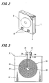
- FIG. 2 is a perspective view of the coil module apparatus according to the first embodiment after assembly.
- the coil module apparatus according to the present embodiment includes a first case piece 1, a second case piece 2 and a secondary side transfer coil 3.
- the first case piece 1 and second case piece 2 are formed of ABS (Acrylonitrile Butadiene Styrene copolymer) resin or the like and form an internal enclosure when placed facing one another and connected to one another.
- the secondary side transfer coil 3 has a flat shape and charges a battery pack of the mobile phone unit based on transfer power transferred from a primary side transfer coil of a cradle apparatus during contactless charging.
- the coil module apparatus further includes a circuit board 4, a temperature sensor 5, a double-sided tape sheet 6, and a magnetic sheet 7.
- the circuit board 4 carries out charging control during contactless charging, control over the transmission and reception of predetermined data, and the like.
- the temperature sensor 5 detects the temperature of the secondary side transfer coil 3 during contactless charging.
- the double-sided tape sheet 6 is provided so as to cover the secondary side transfer coil 3 from the opposite side to the first case piece 1.
- the magnetic sheet 7 is stuck onto the secondary side transfer coil 3 via the double-sided tape sheet 6 so as to cover the secondary side transfer coil 3.
- the coil module apparatus further includes a double-sided tape sheet 8 and a metal sheet 9.
- the double-sided tape sheet 8 is stuck onto the magnetic sheet 7.
- the metal sheet 9 is stuck onto the secondary side transfer coil 3 via the double-sided tape sheet 8 and the magnetic sheet 7 so as to cover the secondary side transfer coil 3. That is, the magnetic sheet 7 and the metal sheet 9 are stuck in that order on the secondary side transfer coil 3 via the double-sided tape sheet 6 and the double-sided tape sheet 8, respectively.
- Connection terminals 10 are provided on the second case piece 2 and when the coil module apparatus is attached to the mobile phone unit, the connection terminals 10 are connected to connection terminals provided on the mobile phone unit for the electrical continuity of the secondary side transfer coil 3, the circuit board 4, and the temperature sensor 5.
- the first case piece 1 and the second case piece 2 are placed facing one another and connected to one another with the components from the secondary side transfer coil 3 to the metal sheet 9 enclosed therein and by doing so, a rectangular box-shaped coil module apparatus as shown in FIG. 2 is formed.
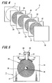
- the secondary side transfer coil 3 is formed by sticking a flat coil, which is produced by winding a wire 20 such as a solid wire or stranded wire with an insulating layer formed on the surface thereof into a spiral on a substantially flat plane, via an adhesive sheet onto a flexible printed circuit board 21.
- the flexible printed circuit board 21 is an extremely thin sheet-like circuit board made of a material such as polyimide resin and has a surface insulating layer formed thereon.
- the surface insulating layer is formed on the surface excluding a first coil connecting portion 23, a second coil connecting portion 25, and a first external connection terminal portion 26, and a second external connection terminal portion 27.
- the first coil connecting portion 23 is located inside an inner periphery portion 22 of the flat coil when the flat coil has been stuck to the flexible printed circuit board 21.
- the second coil connecting portion 25 is located in a periphery outside an outer periphery portion 24 of the flat coil when the flat coil has been stuck to the flexible printed circuit board 21.
- the first coil connecting portion 23 and the first external connection terminal portion 26 are electrically connected via a first internal wiring pattern 28 formed under the surface insulating layer.
- the second coil connecting portion 25 and the second external connection terminal portion 27 are electrically connected via a second internal wiring pattern 29 formed under the surface insulating layer.
- the secondary side transfer coil 3 has no parts where the wire 20 overlaps itself, so that the thickness of the secondary side transfer coil 3 can be made extremely thin.
- the magnetic sheet 7 and the metal sheet 9 are stuck via the double-sided tape sheet 6 and the double-sided tape sheet 8 respectively on the opposite surface of the secondary side transfer coil 3 to the surface on the first case piece 1-side.
- the magnetic sheet 7 and the metal sheet 9 are provided to efficiently form magnetic paths for the secondary side transfer coil 3 to increase the magnetic flux during contactless charging and also suppress unnecessary radiation due to magnetic fields produced during contactless charging.
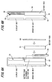
- a flat coil with a multilayer structure formed by stacking a plurality of flexible printed circuit boards on which flat coil patterns made of spiral conductive patterns have been formed may be used as the secondary side transfer coil 3 other than a flat coil formed using the wire 20 as shown in FIG. 3 .
- the secondary side transfer coil 3 includes a four-layer structure.
- a first layer circuit board 31, a second layer circuit board 32, a third layer circuit board 33, and a fourth layer circuit board 34 are respectively formed of wiring conductive patterns 35 that have been wound in spirals on sheet-like circuit boards of a material such as polyimide resin.
- a surface insulating layer 36 is formed on a surface of the first layer circuit board 31 as a topmost layer, and an adhesive layer and an insulating interlayer are formed in between the first layer circuit board 31 and the second layer circuit board 32.
- an adhesive layer and an insulating interlayer are formed in between the second layer circuit board 32 and the third layer circuit board 33 and an adhesive layer and an insulating interlayer are formed in between the third layer circuit board 33 and the fourth layer circuit board 34.
- the magnetic sheet 7 and the metal sheet 9 are stuck onto the rear surface of the fourth layer circuit board 34 that is the bottommost layer via an adhesive layer and an insulating interlayer.
- pattern ends of inner periphery portions 37 of conductive patterns 35 on the first layer circuit board 31 to the fourth layer circuit board 34 are electrically connected via first through-holes 38.
- pattern ends of outer periphery portions 39 of the conductive patterns 35 on the first layer circuit board 31 to the fourth layer circuit board 34 are electrically connected via second through-holes 40.
- first through-holes 38 on the inner periphery portion 37 side of the conductive patterns 35 on each layer are electrically connected to third through-holes 41 provided on the outer periphery portion 39 side of the conductive patterns 35 on each layer.
- the second through-holes 40 of the fourth layer circuit board 34 are electrically connected via a second internal conductive pattern 42 to a second external connecting terminal portion 44.
- the first through-holes 38 of the fourth layer circuit board 34 are electrically connected via the third through-holes 41 and a first internal conductive pattern 43 to a first external connecting terminal portion 45.
- the flat coil is formed by the conductive patterns 35 of the flexible printed circuit boards 31 to 34 on each layer, and therefore the thickness can be made even slimmer than the flat coil that uses the wire 20 described earlier.
- FIG. 6A is a cross-sectional view of a mobile phone unit in which a coil module apparatus 50 is installed.
- the mobile phone unit is a stick-shaped mobile phone unit and includes a battery pack attachment hole portion 52 that encloses a battery pack 51 on a rear surface of an operation unit and a coil module hole portion 53 that encloses the coil module apparatus 50 on a rear surface of a display unit.
- connection terminals 10 provided on the coil module apparatus 50 and connection terminals provided on the mobile phone unit are in contact and electrically connected.
- the battery pack 51 is attached to the battery pack attachment hole portion 52 of the mobile phone unit and then the rear cover 54 is attached.
- the coil module apparatus 50 is attached inside the mobile phone unit.
- the coil module apparatus 50 is attached to the rear surface of the display unit in this example.
- an insertion hole portion for the coil module apparatus 50 may instead be provided on a base surface portion 55 of the mobile terminal shown in FIG. 6A . Accordingly, by inserting the coil module apparatus 50 via this insertion hole portion, the coil module apparatus 50 can be attached between the battery pack 51 and the rear cover 54.
- the insertion hole portion of the coil module apparatus 50 may be provided on a side surface portion of the mobile phone unit and the coil module apparatus 50 may be attached via the insertion hole portion from the side surface portion of the mobile phone unit.
- the first case piece 1 and the second case piece 2 are placed facing one another and connected with the components from the secondary side transfer coil 3 to the metal sheet 9 enclosed therein to assemble a flat coil into a module.
- the resistance to bending and the strength of a flat coil that has been made slim can be obtained with the first case piece 1 and the second case piece 2.
- the coil module apparatus may only need to be inserted inside the mobile phone unit, so that the flat coil is incorporated in a simplified manner. Accordingly, the ease and productivity of the incorporating process can be improved.
- the first case piece 1 and the second case piece 2 are formed so as to enclose the components from the secondary side transfer coil 3 to the metal sheet 9 in the coil module apparatus according to the first embodiment.
- a coil module apparatus according to a second embodiment is formed using a rear cover of a charged appliance, such as a mobile phone unit, as the first case piece 1 described above.
- FIG. 7 is an exploded perspective view of the coil module apparatus according to the second embodiment
- FIG. 8 is a perspective view of the coil module apparatus according to the second embodiment after assembly.
- the coil module apparatus according to the second embodiment is formed so that the components from the secondary side transfer coil 3 to the metal sheet 9 are enclosed by the rear cover 54 of the mobile phone unit shown in FIG. 6A and FIG. 6B and the second case piece 2 described above.
- the coil module apparatus according to the second embodiment uses the rear cover 54 of the mobile phone unit in place of the first case piece 1 described above.
- the coil module apparatus according to the second embodiment is formed so as to enclose components from the secondary side transfer coil 3 to the metal sheet 9 in an enclosure region internally formed by placing the rear cover 54 and the second case piece 2 facing one another.
- FIG. 9A is a cross-sectional view of a mobile phone unit to which a coil module apparatus 60 according to the second embodiment is attached.
- the mobile phone unit is a stick-shaped mobile phone unit, and includes, on a rear surface of an operation unit, a battery pack attachment hole portion 52 that encloses the battery pack 51 and a coil module gap portion 61 that encloses the coil module apparatus 60.
- the coil module apparatus 60 When the coil module apparatus 60 is attached to such a mobile phone unit, after the battery pack 51 has been attached to the battery pack attachment hole portion 52, the coil module apparatus 60 is attached to the mobile phone unit by attaching the rear cover to the mobile phone unit. By doing so, as shown in FIG. 9B , using the rear cover 54 in place of the first case piece 1 in addition to using it as the cover of the mobile phone unit, the coil module apparatus 60 is enclosed inside the coil module gap portion 61, thereby attaching the coil module apparatus to the mobile phone unit.
- the first case piece 1 that forms the coil module apparatus is also used as the rear cover of a charged appliance such as a mobile phone unit, which makes it possible to reduce the number of components, in addition to achieving the same effect as the first embodiment described earlier.
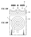
- a groove portion 70 into which the secondary side transfer coil 3 is fitted may be provided on the first case piece 1 or on the rear cover 54 of the mobile phone unit (or charged appliance).
- the groove portion 70 is formed in accordance with the overall form of the secondary side transfer coil 3 formed by the wire 20. This means that by fitting the secondary side transfer coil 3 into the groove portion 70, the secondary side transfer coil 3 can be fixed to the first case piece 1 or the rear cover 54 with the secondary side transfer coil 3 correctly positioned. Also, with the groove portion 70, the positioning on the first case piece I or the rear cover 54 can be simplified.
- the secondary side transfer coil 3 may be insert molded inside the first case piece 1 or the rear cover 54 of the mobile phone unit (or charged appliance). By doing so, it is possible to fix the secondary side transfer coil 3 to the first case piece 1 or the rear cover 54 having correctly positioned the secondary side transfer coil 3 and to also prevent short circuits for the secondary side transfer coil 3. In addition, it is possible to omit a structure for positioning the secondary side transfer coil 3 that is provided on the first case piece 1 or the rear cover 54.
- the magnetic sheet 7 and/or the metal sheet 9 may be insert molded inside the second case piece 2.
- the magnetic sheet 7 and the metal sheet 9 become sealed inside the second case piece 2, it is possible to prevent conductive particles from dispersing from the magnetic sheet 7 and the metal sheet 9.
- the circuit board 4 may be insert molded inside the first case piece 1, the second case piece 2, or the rear cover 54. By doing so, it is possible to easily position and dispose the circuit board 4, and since the circuit board 4 becomes sealed inside the first case piece 1, the second case piece 2, or the rear cover 54, it is possible to prevent short circuits for the circuit board 4.
- the temperature sensor 5 may be insert molded inside the first case piece 1, the second case piece 2, or the rear cover 54. By doing so, it is possible to easily position and dispose the temperature sensor 5, and since the temperature sensor 5 becomes sealed inside the first case piece 1, the second case piece 2, or the rear cover 54, it is possible to prevent short circuits for the temperature sensor 5.
- a multilayer circuit board may be used as the circuit board 4.
- the temperature sensor 5 may be provided between any of the layers of the multilayer circuit board, and the multilayer circuit board provided with the temperature sensor 5 may be insert molded inside the first case piece 1, the second case piece 2, or the rear cover 54. By doing so, it is possible to easily position and dispose the circuit board 4 and the temperature sensor 5, and since the circuit board 4 and the temperature sensor 5 become sealed inside the first case piece 1, the second case piece 2, or the rear cover 54, it is possible to prevent short circuits for the circuit board 4 and the temperature sensor 5.
- the entire second case piece 2 or a surface portion of the second case piece 2 that faces the secondary side transfer coil 3 may be formed of a resin in which a magnetic material is mixed.
- the magnetic sheet 7 shown in FIG. 1 or in FIG. 7 can be omitted, and therefore the coil module apparatus can be made even slimmer. Also, since a magnetic material is mixed into the resin, it is possible to prevent conductive particles from dispersing.
- the surface portion of the second case piece 2 that faces the secondary side transfer coil 3 may be formed of a resin in which a magnetic material is mixed and the other surface portion of the second case piece 2 may be formed of normal resin, or in other words, the second case piece 2 may be dual-molded.
- the magnetic sheet 7 shown in FIG. 1 and FIG. 7 it is possible to omit the magnetic sheet 7 shown in FIG. 1 and FIG. 7 , and therefore the coil module apparatus can be made even slimmer.
- the magnetic material is mixed into the resin, it is possible to prevent conductive particles from dispersing.
- the surface portion of the second case piece 2 that faces the secondary side transfer coil 3 may be formed of a resin in which a magnetic material is mixed and the other surface portion thereof may be formed of normal resin.
- the second case piece 2 may be dual-molded.
- the metal sheet 9 may be insert molded inside the second case piece 2.
- the enclosure region of the case pieces 1 and 2 can be made smaller by an amount corresponding to the magnetic sheet 7 and the metal sheet 9, and therefore the coil module apparatus can be made even slimmer.
- a magnetic material is mixed into the resin and the metal sheet 9 is insert molded inside the second case piece 2, it is possible to prevent conductive particles from dispersing.
- the first case piece 1, the second case piece 2, or the rear cover 54 may be dual-molded of a resin in which a magnetic material is mixed and a normal resin, and the secondary side transfer coil 3 may be insert molded between the resin in which the magnetic material is mixed and the normal resin.
- the second case piece 2 may be formed of an elastic resin, i.e., a resin that exhibits elasticity.
- the rear cover 54 (or the first case piece 1) is dual molded of the normal resin and the resin in which the magnetic material is mixed.
- the secondary side transfer coil 3 and the metal sheet 9 are insert molded, and the second case piece 2 formed of the elastic resin is connected to the rear cover 54.
- the battery pack 51 will expand somewhat due to repeated charging.
- the second case piece 2 that contacts the battery pack 51 being formed of elastic resin, it will be possible to absorb the expansion of the battery pack 51.
- the present invention has been applied to a coil module apparatus of a mobile phone unit in the embodiments described above, the present invention can be applied to a coil module apparatus for a PHS (Personal Handyphone System) telephone, a PDA (Personal Digital Assistant), a mobile game device, a digital camera apparatus, or a notebook computer. By doing so, the same effects as described above can be obtained.
- a PHS Personal Handyphone System
- PDA Personal Digital Assistant
Landscapes
- Engineering & Computer Science (AREA)
- Power Engineering (AREA)
- Telephone Set Structure (AREA)
- Coils Or Transformers For Communication (AREA)
Abstract
Description
- The present invention relates to a coil module apparatus.
- Japanese Patent Application Publication No.
2006-339329 pages 7 to 8 andFIG. 1 ). With this flat coil apparatus, a spiral coil is formed so as to be disposed on a circuit board and a so-called return conductor formed in a direction that traverses the coil in the radial direction from the center to the outer periphery is formed by a printed circuit on the circuit board. By using a printed circuit as the return conductor, it is possible to minimize the thickness of the flat coil apparatus, and to make the entire flat coil apparatus sufficiently slim. - However, when using a slim coil such as one in the flat coil apparatus disclosed in Japanese Patent Application Publication No.
2006-339329 - Further, in the flat coil apparatus disclosed in Japanese Patent Application Publication No.
2006-339329 - It is desirable to provide a coil module apparatus capable of maintaining the resistance to bending and the strength of a coil that has been made slim and of being easily incorporated in an appliance.
- According to an embodiment of the invention, there is provided a coil module apparatus. The coil module apparatus includes: a flat coil having a flat shape; a circuit board for the flat coil; a magnetic sheet provided so as to cover one surface portion of the flat coil; connection terminals for connecting the flat coil and the circuit board; and a case that encloses the flat coil, the circuit board, and the magnetic sheet and encloses the connection terminals so that the connection terminals are partly exposed.
- According to an embodiment of the invention, the flat coil is assembled into a module by enclosing the flat coil and the like inside a case. By enclosing the flat coil inside the case, it is possible to obtain the resistance to bending and the strength of the flat coil. In addition, by assembling the flat coil into a module, the flat coil can be incorporated in a charged appliance in a simplified manner.
- According to an embodiment of the invention, since the flat coil and the like are incorporated in a case and therefore the resistance to bending and the strength of the flat coil can be obtained. Also, since the flat coil is assembled into a module, the flat coil can be incorporated in a charged appliance in a simplified manner.
- Preferably, the coil module apparatus is suitably applied to a contactless power transferring coil that carries out contactless charging of a charged appliance such as a mobile phone unit, a PHS (Personal Handyphone System) telephone, a PDA (Personal Digital Assistant), a mobile game device, a digital camera apparatus, a notebook personal computer or the like. In particular, the present invention relates to a coil module apparatus which, by assembling a flat coil that has been made slim into a module, has improved resistance to bending and improved strength and can be easily installed in a charged appliance.
- Various respective aspects and features of the invention are defined in the appended claims. Combinations of features from the dependent claims may be combined with features of the independent claims as appropriate and not merely as explicitly set out in the claims.
- Embodiments of the invention will now be described with reference to the accompanying drawings, throughout which like parts are referred to by like references, and in which:
-
FIG. 1 is an exploded perspective view of a coil module apparatus according to a first embodiment of the present invention. -
FIG. 2 is a perspective view of a coil module apparatus according to the first embodiment of the present invention. -
FIG. 3 is a view used for explaining a flat coil formed using a wire. -
FIG. 4 is an exploded perspective view of a flat coil with a multilayer structure formed by stacking a plurality of flexible printed circuit boards on which conductive patterns are formed. -
FIG. 5 is a view used for explaining the connections between the conductive patterns of a flat coil having a multilayer structure. -
FIGS. 6A and 6B are views used for explaining a process of attaching the coil module apparatus according to the first embodiment of the present invention to a mobile phone unit. -
FIG. 7 is an exploded perspective view of a coil module apparatus according to a second embodiment of the present invention. -
FIG. 8 is a perspective view of the coil module apparatus according to the second embodiment. -
FIGS. 9A and 9B are views used for explaining a process of attaching the coil module apparatus according to the second embodiment of the present invention to a mobile phone unit. -
FIGS. 10A and 10B are views used for explaining a first modification where a groove portion into which the flat coil is fitted is formed in a case. -
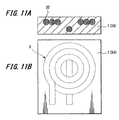
FIGS. 11A and 11B are views used for explaining a second modification where the flat coil is insert molded inside the case. -
FIGS. 12A and 12B are views used for explaining a third modification where a magnetic sheet and/or metal sheet are insert molded inside the case. -
FIGS. 13A and 13B are views used for explaining a fourth modification where the circuit board is insert molded inside the case. -
FIGS. 14A and 14B are views used for explaining a fifth modification where a temperature sensor is insert molded inside the case. -
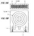
FIGS. 15A and 15B are views used for explaining a sixth modification where a temperature sensor is provided between any two layers of a multilayer circuit board and the multilayer circuit board provided with the temperature sensor is insert molded inside the case. -
FIG. 16 is a view used for explaining a seventh modification where a surface portion of the case is formed of a resin in which a magnetic material is mixed. -
FIG. 17 is a view used for explaining an eighth modification where the case is dual-molded of a resin in which a magnetic material is mixed and a normal resin. -
FIG. 18 is a view used for explaining a ninth modification where the case is dual-molded of a resin in which a magnetic material is mixed and a normal resin and where a metal sheet is insert molded. -
FIG. 19 is a view used for explaining a tenth modification where the case is dual-molded with a resin in which a magnetic material is mixed and a normal resin and where the secondaryside transfer coil 3 is insert molded. -
FIG. 20 is a view used for explaining an eleventh modification where the case is formed of elastic resin. - Embodiments of the present invention can be applied to a coil module apparatus that realizes a contactless charging function when incorporated in a mobile phone unit.
-
FIG. 1 is an exploded perspective view of a coil module apparatus according to a first embodiment of the present invention andFIG. 2 is a perspective view of the coil module apparatus according to the first embodiment after assembly. As can be understood fromFIG. 1 andFIG. 2 , the coil module apparatus according to the present embodiment includes afirst case piece 1, asecond case piece 2 and a secondaryside transfer coil 3. Thefirst case piece 1 andsecond case piece 2 are formed of ABS (Acrylonitrile Butadiene Styrene copolymer) resin or the like and form an internal enclosure when placed facing one another and connected to one another. The secondaryside transfer coil 3 has a flat shape and charges a battery pack of the mobile phone unit based on transfer power transferred from a primary side transfer coil of a cradle apparatus during contactless charging. - The coil module apparatus further includes a
circuit board 4, atemperature sensor 5, a double-sided tape sheet 6, and amagnetic sheet 7. Thecircuit board 4 carries out charging control during contactless charging, control over the transmission and reception of predetermined data, and the like. Thetemperature sensor 5 detects the temperature of the secondaryside transfer coil 3 during contactless charging. The double-sided tape sheet 6 is provided so as to cover the secondaryside transfer coil 3 from the opposite side to thefirst case piece 1. Themagnetic sheet 7 is stuck onto the secondaryside transfer coil 3 via the double-sided tape sheet 6 so as to cover the secondaryside transfer coil 3. - The coil module apparatus further includes a double-
sided tape sheet 8 and ametal sheet 9. The double-sided tape sheet 8 is stuck onto themagnetic sheet 7. Themetal sheet 9 is stuck onto the secondaryside transfer coil 3 via the double-sided tape sheet 8 and themagnetic sheet 7 so as to cover the secondaryside transfer coil 3. That is, themagnetic sheet 7 and themetal sheet 9 are stuck in that order on the secondaryside transfer coil 3 via the double-sided tape sheet 6 and the double-sided tape sheet 8, respectively. -
Connection terminals 10 are provided on thesecond case piece 2 and when the coil module apparatus is attached to the mobile phone unit, theconnection terminals 10 are connected to connection terminals provided on the mobile phone unit for the electrical continuity of the secondaryside transfer coil 3, thecircuit board 4, and thetemperature sensor 5. - The
first case piece 1 and thesecond case piece 2 are placed facing one another and connected to one another with the components from the secondaryside transfer coil 3 to themetal sheet 9 enclosed therein and by doing so, a rectangular box-shaped coil module apparatus as shown inFIG. 2 is formed. - As shown in
FIG. 3 , the secondaryside transfer coil 3 is formed by sticking a flat coil, which is produced by winding awire 20 such as a solid wire or stranded wire with an insulating layer formed on the surface thereof into a spiral on a substantially flat plane, via an adhesive sheet onto a flexible printedcircuit board 21. - The flexible printed
circuit board 21 is an extremely thin sheet-like circuit board made of a material such as polyimide resin and has a surface insulating layer formed thereon. The surface insulating layer is formed on the surface excluding a firstcoil connecting portion 23, a secondcoil connecting portion 25, and a first externalconnection terminal portion 26, and a second externalconnection terminal portion 27. The firstcoil connecting portion 23 is located inside aninner periphery portion 22 of the flat coil when the flat coil has been stuck to the flexible printedcircuit board 21. The secondcoil connecting portion 25 is located in a periphery outside anouter periphery portion 24 of the flat coil when the flat coil has been stuck to the flexible printedcircuit board 21. - The first
coil connecting portion 23 and the first externalconnection terminal portion 26 are electrically connected via a firstinternal wiring pattern 28 formed under the surface insulating layer. Similarly, the secondcoil connecting portion 25 and the second externalconnection terminal portion 27 are electrically connected via a secondinternal wiring pattern 29 formed under the surface insulating layer. - When the flat coil is stuck onto the flexible printed
circuit board 21, a winding start portion in theinner periphery portion 22 is electrically connected to the firstcoil connecting portion 23 and a winding end portion of theouter periphery portion 24 is electrically connected to the secondcoil connecting portion 25. With this construction, the secondaryside transfer coil 3 has no parts where thewire 20 overlaps itself, so that the thickness of the secondaryside transfer coil 3 can be made extremely thin. - The
magnetic sheet 7 and themetal sheet 9 are stuck via the double-sided tape sheet 6 and the double-sided tape sheet 8 respectively on the opposite surface of the secondaryside transfer coil 3 to the surface on the first case piece 1-side. Themagnetic sheet 7 and themetal sheet 9 are provided to efficiently form magnetic paths for the secondaryside transfer coil 3 to increase the magnetic flux during contactless charging and also suppress unnecessary radiation due to magnetic fields produced during contactless charging. - As shown in
FIG. 4 , a flat coil with a multilayer structure formed by stacking a plurality of flexible printed circuit boards on which flat coil patterns made of spiral conductive patterns have been formed may be used as the secondaryside transfer coil 3 other than a flat coil formed using thewire 20 as shown inFIG. 3 . - In this case, the secondary
side transfer coil 3 includes a four-layer structure. For example, a firstlayer circuit board 31, a secondlayer circuit board 32, a thirdlayer circuit board 33, and a fourthlayer circuit board 34 are respectively formed of wiringconductive patterns 35 that have been wound in spirals on sheet-like circuit boards of a material such as polyimide resin. - A
surface insulating layer 36 is formed on a surface of the firstlayer circuit board 31 as a topmost layer, and an adhesive layer and an insulating interlayer are formed in between the firstlayer circuit board 31 and the secondlayer circuit board 32. In the same way, an adhesive layer and an insulating interlayer are formed in between the secondlayer circuit board 32 and the thirdlayer circuit board 33 and an adhesive layer and an insulating interlayer are formed in between the thirdlayer circuit board 33 and the fourthlayer circuit board 34. Themagnetic sheet 7 and themetal sheet 9 are stuck onto the rear surface of the fourthlayer circuit board 34 that is the bottommost layer via an adhesive layer and an insulating interlayer. - As shown in
FIG. 5 , pattern ends ofinner periphery portions 37 ofconductive patterns 35 on the firstlayer circuit board 31 to the fourthlayer circuit board 34 are electrically connected via first through-holes 38. Similarly, pattern ends ofouter periphery portions 39 of theconductive patterns 35 on the firstlayer circuit board 31 to the fourthlayer circuit board 34 are electrically connected via second through-holes 40. - In addition, the first through-
holes 38 on theinner periphery portion 37 side of theconductive patterns 35 on each layer are electrically connected to third through-holes 41 provided on theouter periphery portion 39 side of theconductive patterns 35 on each layer. - Also, the second through-
holes 40 of the fourthlayer circuit board 34, for example, are electrically connected via a second internalconductive pattern 42 to a second external connectingterminal portion 44. Similarly, the first through-holes 38 of the fourthlayer circuit board 34 are electrically connected via the third through-holes 41 and a first internalconductive pattern 43 to a first external connectingterminal portion 45. - When a flat coil with a multilayer structure is used as the secondary
side transfer coil 3, the flat coil is formed by theconductive patterns 35 of the flexible printedcircuit boards 31 to 34 on each layer, and therefore the thickness can be made even slimmer than the flat coil that uses thewire 20 described earlier. -
FIG. 6A is a cross-sectional view of a mobile phone unit in which acoil module apparatus 50 is installed. As one example, the mobile phone unit is a stick-shaped mobile phone unit and includes a battery packattachment hole portion 52 that encloses abattery pack 51 on a rear surface of an operation unit and a coilmodule hole portion 53 that encloses thecoil module apparatus 50 on a rear surface of a display unit. - When attaching the
coil module apparatus 50 to such a mobile phone unit, arear cover 54 of the mobile phone unit is removed. Subsequently, before thebattery pack 51 is attached, thecoil module apparatus 50 is inserted into the coilmodule hole portion 53 provided on the rear of the display unit as shown by the dotted arrow inFIG. 6A . By doing so, theconnection terminals 10 provided on thecoil module apparatus 50 and connection terminals provided on the mobile phone unit are in contact and electrically connected. - Next, the
battery pack 51 is attached to the battery packattachment hole portion 52 of the mobile phone unit and then therear cover 54 is attached. By doing so, as shown inFIG. 6B , thecoil module apparatus 50 is attached inside the mobile phone unit. - Note that the
coil module apparatus 50 is attached to the rear surface of the display unit in this example. However, an insertion hole portion for thecoil module apparatus 50 may instead be provided on abase surface portion 55 of the mobile terminal shown inFIG. 6A . Accordingly, by inserting thecoil module apparatus 50 via this insertion hole portion, thecoil module apparatus 50 can be attached between thebattery pack 51 and therear cover 54. Alternatively, the insertion hole portion of thecoil module apparatus 50 may be provided on a side surface portion of the mobile phone unit and thecoil module apparatus 50 may be attached via the insertion hole portion from the side surface portion of the mobile phone unit. - As is clear from the above description, in the coil module apparatus according to the first embodiment, the
first case piece 1 and thesecond case piece 2 are placed facing one another and connected with the components from the secondaryside transfer coil 3 to themetal sheet 9 enclosed therein to assemble a flat coil into a module. By doing so, the resistance to bending and the strength of a flat coil that has been made slim can be obtained with thefirst case piece 1 and thesecond case piece 2. Since the flat coil is provided as a module, when attached to a mobile phone unit, the coil module apparatus may only need to be inserted inside the mobile phone unit, so that the flat coil is incorporated in a simplified manner. Accordingly, the ease and productivity of the incorporating process can be improved. - Also, since a process that inserts the coil module apparatus into a charged appliance such as a mobile phone unit is sufficient as the incorporating process, it is possible to easily provide a contactless charging function to only charged appliances that may actually require such contactless charging function.
- The
first case piece 1 and thesecond case piece 2 are formed so as to enclose the components from the secondaryside transfer coil 3 to themetal sheet 9 in the coil module apparatus according to the first embodiment. In contrast, a coil module apparatus according to a second embodiment is formed using a rear cover of a charged appliance, such as a mobile phone unit, as thefirst case piece 1 described above. - Note that parts of the coil module apparatus according to the second embodiment that are the same as those in the coil module apparatus according to the first embodiment described earlier have been assigned the same reference numerals in the drawings used to describe the coil module apparatus according to the second embodiment and duplicated description thereof is omitted.
-
FIG. 7 is an exploded perspective view of the coil module apparatus according to the second embodiment andFIG. 8 is a perspective view of the coil module apparatus according to the second embodiment after assembly. As is understood fromFIG. 7 andFIG. 8 , the coil module apparatus according to the second embodiment is formed so that the components from the secondaryside transfer coil 3 to themetal sheet 9 are enclosed by therear cover 54 of the mobile phone unit shown inFIG. 6A and FIG. 6B and thesecond case piece 2 described above. - That is, the coil module apparatus according to the second embodiment uses the
rear cover 54 of the mobile phone unit in place of thefirst case piece 1 described above. The coil module apparatus according to the second embodiment is formed so as to enclose components from the secondaryside transfer coil 3 to themetal sheet 9 in an enclosure region internally formed by placing therear cover 54 and thesecond case piece 2 facing one another. -
FIG. 9A is a cross-sectional view of a mobile phone unit to which acoil module apparatus 60 according to the second embodiment is attached. As one example, the mobile phone unit is a stick-shaped mobile phone unit, and includes, on a rear surface of an operation unit, a battery packattachment hole portion 52 that encloses thebattery pack 51 and a coilmodule gap portion 61 that encloses thecoil module apparatus 60. - When the
coil module apparatus 60 is attached to such a mobile phone unit, after thebattery pack 51 has been attached to the battery packattachment hole portion 52, thecoil module apparatus 60 is attached to the mobile phone unit by attaching the rear cover to the mobile phone unit. By doing so, as shown inFIG. 9B , using therear cover 54 in place of thefirst case piece 1 in addition to using it as the cover of the mobile phone unit, thecoil module apparatus 60 is enclosed inside the coilmodule gap portion 61, thereby attaching the coil module apparatus to the mobile phone unit. - As is clear from the above description, in the coil module apparatus according to the second embodiment, the
first case piece 1 that forms the coil module apparatus is also used as the rear cover of a charged appliance such as a mobile phone unit, which makes it possible to reduce the number of components, in addition to achieving the same effect as the first embodiment described earlier. - Modifications of the embodiments described above will now be described. Note that the modifications described below may be individually or collectively applied to the coil module apparatuses of the embodiments described earlier.
- As shown in
FIG. 10A and FIG. 10B , in the coil module apparatuses according to the embodiments described above, agroove portion 70 into which the secondaryside transfer coil 3 is fitted may be provided on thefirst case piece 1 or on therear cover 54 of the mobile phone unit (or charged appliance). Thegroove portion 70 is formed in accordance with the overall form of the secondaryside transfer coil 3 formed by thewire 20. This means that by fitting the secondaryside transfer coil 3 into thegroove portion 70, the secondaryside transfer coil 3 can be fixed to thefirst case piece 1 or therear cover 54 with the secondaryside transfer coil 3 correctly positioned. Also, with thegroove portion 70, the positioning on the first case piece I or therear cover 54 can be simplified. - As shown in
FIG. 11A and FIG. 11B , in the coil module apparatuses according to the embodiments described above, the secondaryside transfer coil 3 may be insert molded inside thefirst case piece 1 or therear cover 54 of the mobile phone unit (or charged appliance). By doing so, it is possible to fix the secondaryside transfer coil 3 to thefirst case piece 1 or therear cover 54 having correctly positioned the secondaryside transfer coil 3 and to also prevent short circuits for the secondaryside transfer coil 3. In addition, it is possible to omit a structure for positioning the secondaryside transfer coil 3 that is provided on thefirst case piece 1 or therear cover 54. - As shown in
FIG. 12A and FIG. 12B , in the coil module apparatuses according to the embodiments described above, themagnetic sheet 7 and/or themetal sheet 9 may be insert molded inside thesecond case piece 2. By doing so, since themagnetic sheet 7 and themetal sheet 9 become sealed inside thesecond case piece 2, it is possible to prevent conductive particles from dispersing from themagnetic sheet 7 and themetal sheet 9. - As shown in
FIG. 13A and FIG. 13B , in the coil module apparatuses according to the embodiments described above, thecircuit board 4 may be insert molded inside thefirst case piece 1, thesecond case piece 2, or therear cover 54. By doing so, it is possible to easily position and dispose thecircuit board 4, and since thecircuit board 4 becomes sealed inside thefirst case piece 1, thesecond case piece 2, or therear cover 54, it is possible to prevent short circuits for thecircuit board 4. - As shown in
FIG. 14A and FIG. 14B , in the coil module apparatuses according to the embodiments described above, thetemperature sensor 5 may be insert molded inside thefirst case piece 1, thesecond case piece 2, or therear cover 54. By doing so, it is possible to easily position and dispose thetemperature sensor 5, and since thetemperature sensor 5 becomes sealed inside thefirst case piece 1, thesecond case piece 2, or therear cover 54, it is possible to prevent short circuits for thetemperature sensor 5. - As shown in
FIG. 15A and FIG. 15B , in the coil module apparatuses according to the embodiments described above, a multilayer circuit board may be used as thecircuit board 4. Thetemperature sensor 5 may be provided between any of the layers of the multilayer circuit board, and the multilayer circuit board provided with thetemperature sensor 5 may be insert molded inside thefirst case piece 1, thesecond case piece 2, or therear cover 54. By doing so, it is possible to easily position and dispose thecircuit board 4 and thetemperature sensor 5, and since thecircuit board 4 and thetemperature sensor 5 become sealed inside thefirst case piece 1, thesecond case piece 2, or therear cover 54, it is possible to prevent short circuits for thecircuit board 4 and thetemperature sensor 5. - As shown in
FIG. 16 , in the coil module apparatuses according to the embodiments described above, the entiresecond case piece 2 or a surface portion of thesecond case piece 2 that faces the secondaryside transfer coil 3 may be formed of a resin in which a magnetic material is mixed. In this case, themagnetic sheet 7 shown inFIG. 1 or inFIG. 7 can be omitted, and therefore the coil module apparatus can be made even slimmer. Also, since a magnetic material is mixed into the resin, it is possible to prevent conductive particles from dispersing. - As shown in
FIG. 17 , in the coil module apparatuses according to the embodiments described above, the surface portion of thesecond case piece 2 that faces the secondaryside transfer coil 3 may be formed of a resin in which a magnetic material is mixed and the other surface portion of thesecond case piece 2 may be formed of normal resin, or in other words, thesecond case piece 2 may be dual-molded. In this case, it is possible to omit themagnetic sheet 7 shown inFIG. 1 andFIG. 7 , and therefore the coil module apparatus can be made even slimmer. Also, since the magnetic material is mixed into the resin, it is possible to prevent conductive particles from dispersing. - As shown in
FIG. 18 , in the coil module apparatuses according to the embodiments described above, the surface portion of thesecond case piece 2 that faces the secondaryside transfer coil 3 may be formed of a resin in which a magnetic material is mixed and the other surface portion thereof may be formed of normal resin. In other words, thesecond case piece 2 may be dual-molded. Themetal sheet 9 may be insert molded inside thesecond case piece 2. In this case, the enclosure region of thecase pieces magnetic sheet 7 and themetal sheet 9, and therefore the coil module apparatus can be made even slimmer. Also, since a magnetic material is mixed into the resin and themetal sheet 9 is insert molded inside thesecond case piece 2, it is possible to prevent conductive particles from dispersing. - As shown in
FIG. 19 , in the coil module apparatuses according to the embodiments described above, thefirst case piece 1, thesecond case piece 2, or therear cover 54 may be dual-molded of a resin in which a magnetic material is mixed and a normal resin, and the secondaryside transfer coil 3 may be insert molded between the resin in which the magnetic material is mixed and the normal resin. By doing so, it is possible to obtain the effects of dual molding and the effects of insert molding the secondaryside transfer coil 3 described above. - As shown in
FIG. 20 , in the coil module apparatuses according to the embodiments described above, thesecond case piece 2 may be formed of an elastic resin, i.e., a resin that exhibits elasticity. In the example shown inFIG. 20 , the rear cover 54 (or the first case piece 1) is dual molded of the normal resin and the resin in which the magnetic material is mixed. The secondaryside transfer coil 3 and themetal sheet 9 are insert molded, and thesecond case piece 2 formed of the elastic resin is connected to therear cover 54. - It is known that the
battery pack 51 will expand somewhat due to repeated charging. With thesecond case piece 2 that contacts thebattery pack 51 being formed of elastic resin, it will be possible to absorb the expansion of thebattery pack 51. - Although the present invention has been applied to a coil module apparatus of a mobile phone unit in the embodiments described above, the present invention can be applied to a coil module apparatus for a PHS (Personal Handyphone System) telephone, a PDA (Personal Digital Assistant), a mobile game device, a digital camera apparatus, or a notebook computer. By doing so, the same effects as described above can be obtained.
- The embodiments and modifications described above are mere examples of the present invention and the present invention is not limited to such embodiments and modifications. It should therefore be understood by those skilled in the art that various modifications, combinations, sub-combinations and alterations may occur depending on design requirements and other factors insofar as they are within the scope of the appended claims.
- In so far as the embodiments of the invention described above are implemented, at least in part, using software-controlled data processing apparatus, it will be appreciated that a computer program providing such software control and a transmission, storage or other medium by which such a computer program is provided are envisaged as aspects of the present invention.
Claims (17)
- A coil module apparatus comprising:a flat coil having a flat shape;a circuit board for the flat coil;a magnetic sheet provided so as to cover one surface portion of the flat coil;connection terminals for connecting the flat coil and the circuit board; anda case that encloses the flat coil, the circuit board, and the magnetic sheet and encloses the connection terminals so that the connection terminals are partly exposed.
- A coil module apparatus according to claim 1, whereinthe flat coil is one of:a flat coil formed by winding a wire composed of one of a conductive single wire and a conductive twisted wire into a spiral on a substantially flat plane, anda flat coil formed by stacking a plurality of conductive pattern circuit boards, on which conductive patterns that each form part of the flat coil are formed, so that a spiral flat coil pattern is formed of the conductive patterns and electrically connecting the conductive patterns.
- A coil module apparatus according to claim 1, whereinthe flat coil enclosed in the case is a flat coil formed by winding a wire composed of one of a conductive single wire and a conductive twisted wire into a spiral on a substantially flat plane, and the case includes a flat coil insertion portion in the form of a groove with a shape that matches the flat coil and is provided in a surface portion contacted by the flat coil.
- A coil module apparatus according to claim 1, whereinthe flat coil, which is formed by winding a wire composed of one of a conductive single wire and a conductive twisted wire into a spiral on a substantially flat plane, is insert molded inside one surface portion of the case.
- A coil module apparatus according to claim 1, whereinthe magnetic sheet is insert molded inside the case.
- A coil module apparatus according to claim 1, whereinthe magnetic sheet is integrally formed with one surface portion of the case by mixing a magnetic material into a predetermined resin that forms the one surface portion of the case.
- A coil module apparatus according to claim 1, whereinthe magnetic sheet is formed by mixing a magnetic material into a predetermined resin, and one surface portion of the case is dual molded of a resin that forms the one surface of the case and the magnetic sheet that is formed by mixing the magnetic material into the predetermined resin.
- A coil module apparatus according to claim 7, whereinthe flat coil is insert molded between the resin that forms the one surface portion of the case and the magnetic sheet that is formed by mixing the magnetic material into the predetermined resin.
- A coil module apparatus according to claim 1, further comprisinga metal sheet that is enclosed inside the case and is provided so as to cover the flat coil from above the magnetic sheet.
- A coil module apparatus according to claim 9, whereinthe metal sheet is insert molded inside the case.
- A coil module apparatus according to claim 10, whereinthe metal sheet is insert molded between resin that forms one surface portion of the case and the magnetic sheet which is formed by mixing a magnetic material into a predetermined resin.
- A coil module apparatus according to claim 1, further comprisinga temperature detecting unit that is enclosed inside the case and detects a temperature of the flat coil.
- A coil module apparatus according to claim 12, whereinthe temperature detecting unit is insert molded inside one surface portion of the case.
- A coil module apparatus according to claim 1, whereinthe circuit board is insert molded inside one surface portion of the case.
- A coil module apparatus according to claim 14, whereinthe circuit board insert molded in the case is composed of a multilayer circuit board and the temperature detecting unit is provided between any two layers of the multilayer circuit board.
- A coil module apparatus according to claim 1, whereina surface portion of the case that contacts a battery pack, which is provided in an appliance to which the coil module apparatus is attached, is formed of elastic resin.
- A coil module apparatus according to claim 1, whereina surface portion of the case that faces an opposite surface portion of the flat coil to the surface portion covered by the magnetic sheet is processed so as to be shaped as a rear cover of a charged appliance to which the coil module apparatus is attached.
Applications Claiming Priority (1)
| Application Number | Priority Date | Filing Date | Title |
|---|---|---|---|
| JP2007141690A JP4896820B2 (en) | 2007-05-29 | 2007-05-29 | Coil module device |
Publications (3)
| Publication Number | Publication Date |
|---|---|
| EP1998342A2 true EP1998342A2 (en) | 2008-12-03 |
| EP1998342A3 EP1998342A3 (en) | 2014-07-09 |
| EP1998342B1 EP1998342B1 (en) | 2018-01-10 |
Family
ID=39712160
Family Applications (1)
| Application Number | Title | Priority Date | Filing Date |
|---|---|---|---|
| EP08251854.9A Active EP1998342B1 (en) | 2007-05-29 | 2008-05-28 | Coil module apparatus |
Country Status (4)
| Country | Link |
|---|---|
| US (1) | US7852184B2 (en) |
| EP (1) | EP1998342B1 (en) |
| JP (1) | JP4896820B2 (en) |
| CN (1) | CN101383215A (en) |
Cited By (7)
| Publication number | Priority date | Publication date | Assignee | Title |
|---|---|---|---|---|
| EP2911166A1 (en) * | 2014-01-29 | 2015-08-26 | Toyota Jidosha Kabushiki Kaisha | Power receiving device and power transmitting device |
| US10340078B2 (en) | 2013-12-17 | 2019-07-02 | Witricity Corporation | Coil topologies for inductive power transfer |
| EP3509078A4 (en) * | 2016-09-02 | 2020-04-29 | IHI Corporation | COIL DEVICE AND SUPPORT MEMBER |
| EP3786988A4 (en) * | 2018-06-11 | 2021-09-01 | Guangdong Oppo Mobile Telecommunications Corp., Ltd. | WIRELESS CHARGING REEL, WIRELESS CHARGING ARRANGEMENT AND ELECTRONIC DEVICE |
| EP3129286B1 (en) * | 2014-04-07 | 2022-03-23 | Safran Seats USA LLC | Inductive power transmission in aircraft seats |
| PL73205Y1 (en) * | 2021-07-15 | 2023-12-04 | Siec Badawcza Lukasiewicz Inst Metali Niezelaznych | Spacer, especially for magnetic chokes |
| US20230412006A1 (en) * | 2022-06-14 | 2023-12-21 | Tdk Taiwan Corp. | Wireless transmission module |
Families Citing this family (34)
| Publication number | Priority date | Publication date | Assignee | Title |
|---|---|---|---|---|
| JP5659504B2 (en) * | 2010-03-02 | 2015-01-28 | 富士通株式会社 | Electromagnetic wave characteristic improvement sheet |
| KR101134625B1 (en) * | 2010-07-16 | 2012-04-09 | 주식회사 한림포스텍 | Core assembly for wireless power transmission, power supplying apparatus for wireless power transmission having the same, and method for manufacturing core assembly for wireless power transmission |
| JP5532422B2 (en) * | 2010-07-30 | 2014-06-25 | スミダコーポレーション株式会社 | coil |
| EP3196903B1 (en) | 2011-01-19 | 2019-05-08 | Technova Inc. | Contactless power transfer apparatus |
| US20130293191A1 (en) | 2011-01-26 | 2013-11-07 | Panasonic Corporation | Non-contact charging module and non-contact charging instrument |
| JP2012178530A (en) * | 2011-02-28 | 2012-09-13 | Equos Research Co Ltd | Antenna |
| JP2012178531A (en) * | 2011-02-28 | 2012-09-13 | Equos Research Co Ltd | Antenna |
| JP2012178529A (en) * | 2011-02-28 | 2012-09-13 | Equos Research Co Ltd | Antenna |
| JP5703842B2 (en) * | 2011-02-28 | 2015-04-22 | 三菱マテリアル株式会社 | Non-contact power supply with temperature sensor |
| EP3425651A3 (en) | 2011-06-14 | 2019-01-16 | Panasonic Corporation | Communication apparatus |
| JP5457478B2 (en) * | 2011-06-14 | 2014-04-02 | パナソニック株式会社 | Mobile device |
| JP2013038893A (en) * | 2011-08-08 | 2013-02-21 | Equos Research Co Ltd | Power transmission system |
| US10204734B2 (en) | 2011-11-02 | 2019-02-12 | Panasonic Corporation | Electronic device including non-contact charging module and near field communication antenna |
| JP5965148B2 (en) * | 2012-01-05 | 2016-08-03 | 日東電工株式会社 | Power receiving module for mobile terminal using wireless power transmission and rechargeable battery for mobile terminal equipped with power receiving module for mobile terminal |
| US8760253B2 (en) * | 2012-01-17 | 2014-06-24 | Delphi Technologies, Inc. | Electrical coil assembly including a ferrite layer and a thermally-conductive silicone layer |
| JP2013169122A (en) | 2012-02-17 | 2013-08-29 | Panasonic Corp | Non-contact charge module and portable terminal having the same |
| JP6112383B2 (en) | 2012-06-28 | 2017-04-12 | パナソニックIpマネジメント株式会社 | Mobile device |
| US9179558B1 (en) | 2012-09-17 | 2015-11-03 | Brite Case, LLC | Case with panel for display |
| JP6034644B2 (en) * | 2012-10-10 | 2016-11-30 | デクセリアルズ株式会社 | Composite coil module and portable device |
| KR101963261B1 (en) | 2013-03-22 | 2019-03-28 | 삼성전기주식회사 | Cordless charging apparatus |
| DE102013210411A1 (en) * | 2013-06-05 | 2014-12-11 | Robert Bosch Gmbh | Coil device and method for inductive power transmission |
| KR101762778B1 (en) | 2014-03-04 | 2017-07-28 | 엘지이노텍 주식회사 | Wireless communication and charge substrate and wireless communication and charge device |
| US9621016B2 (en) * | 2014-08-20 | 2017-04-11 | Apple Inc. | Flat coil assembly for Lorentz actuator mechanism |
| US20160072337A1 (en) * | 2014-09-04 | 2016-03-10 | Samsung Electro-Mechanics Co., Ltd. | Case and apparatus including the same |
| US10643787B2 (en) * | 2015-02-11 | 2020-05-05 | Fu Da Tong Technology Co., Ltd. | Induction type power supply system and coil module thereof |
| KR102484849B1 (en) * | 2015-12-18 | 2023-01-05 | 주식회사 위츠 | Coil assembly |
| USD812556S1 (en) * | 2016-12-02 | 2018-03-13 | Guangdong Bestek E-Commerce Co., Ltd. | Wireless charger |
| CN106451810A (en) * | 2016-12-05 | 2017-02-22 | 青岛鲁渝能源科技有限公司 | Leakage-proof protector and mobile phone charging system |
| KR102703563B1 (en) * | 2017-02-01 | 2024-09-06 | 삼성전자주식회사 | Display system, wireless power transmitter and wireless power receiver |
| US10638031B1 (en) | 2017-03-29 | 2020-04-28 | Apple Inc. | Additive coil structure for voice coil motor actuator |
| US10742093B2 (en) * | 2017-04-11 | 2020-08-11 | Shibaura Electronics Co., Ltd. | Temperature sensor |
| CN107068369A (en) * | 2017-06-01 | 2017-08-18 | 班戈设备系统(苏州)有限公司 | A kind of Anti-radiation transformer |
| KR20210075550A (en) * | 2019-12-13 | 2021-06-23 | 삼성전자주식회사 | Electronic device comprising coils |
| CN115579228A (en) * | 2021-10-28 | 2023-01-06 | 荣耀终端有限公司 | Electronic equipment |
Citations (1)
| Publication number | Priority date | Publication date | Assignee | Title |
|---|---|---|---|---|
| JP2006339329A (en) | 2005-06-01 | 2006-12-14 | Seiko Epson Corp | Planar coil device, substrate, and planar coil fixing method |
Family Cites Families (17)
| Publication number | Priority date | Publication date | Assignee | Title |
|---|---|---|---|---|
| JPS6149423A (en) * | 1984-08-17 | 1986-03-11 | Matsushita Electronics Corp | Manufacture of semiconductor device |
| US5375040A (en) * | 1992-09-29 | 1994-12-20 | Eldec Corporation | Modular electronic circuit housing and wiring board |
| JPH07264779A (en) * | 1994-03-18 | 1995-10-13 | Sony Corp | Electromagnetic induction charging system |
| JPH08148359A (en) * | 1994-11-18 | 1996-06-07 | Tdk Corp | Connector for lan |
| JP3430807B2 (en) * | 1996-07-25 | 2003-07-28 | 松下電工株式会社 | Rechargeable electrical equipment |
| JP3697789B2 (en) * | 1996-09-20 | 2005-09-21 | 松下電器産業株式会社 | Non-contact power supply |
| US5835350A (en) * | 1996-12-23 | 1998-11-10 | Lucent Technologies Inc. | Encapsulated, board-mountable power supply and method of manufacture therefor |
| JP3818478B2 (en) * | 1998-09-08 | 2006-09-06 | シャープ株式会社 | Sheet type transformer, manufacturing method thereof, and switching power supply module including sheet type transformer |
| JP2000269059A (en) * | 1999-03-16 | 2000-09-29 | Nippon Telegr & Teleph Corp <Ntt> | Magnetic component and method of manufacturing the same |
| JP3652936B2 (en) * | 1999-10-12 | 2005-05-25 | 株式会社豊田自動織機 | Charging power supply paddle and manufacturing method of charging power supply paddle |
| JP2002175922A (en) * | 2000-12-08 | 2002-06-21 | Sansha Electric Mfg Co Ltd | High frequency high current transformer |
| EP1547222B1 (en) * | 2002-06-10 | 2018-10-03 | City University of Hong Kong | Planar inductive battery charger |
| JP2005269599A (en) * | 2004-02-18 | 2005-09-29 | Sony Corp | Magnetic core member for antenna module and manufacturing method thereof |
| JP2005260122A (en) * | 2004-03-15 | 2005-09-22 | Dainippon Printing Co Ltd | Non-contact power transmission module |
| JP2006339757A (en) * | 2005-05-31 | 2006-12-14 | Denso Corp | Antenna coil, method for manufacturing communication board module, and card-type radio |
| US7495414B2 (en) * | 2005-07-25 | 2009-02-24 | Convenient Power Limited | Rechargeable battery circuit and structure for compatibility with a planar inductive charging platform |
| US8022801B2 (en) * | 2007-02-20 | 2011-09-20 | Seiko Epson Corporation | Coil unit and electronic instrument |
-
2007
- 2007-05-29 JP JP2007141690A patent/JP4896820B2/en active Active
-
2008
- 2008-05-28 EP EP08251854.9A patent/EP1998342B1/en active Active
- 2008-05-28 US US12/153,935 patent/US7852184B2/en active Active
- 2008-05-29 CN CNA2008101428514A patent/CN101383215A/en active Pending
Patent Citations (1)
| Publication number | Priority date | Publication date | Assignee | Title |
|---|---|---|---|---|
| JP2006339329A (en) | 2005-06-01 | 2006-12-14 | Seiko Epson Corp | Planar coil device, substrate, and planar coil fixing method |
Cited By (10)
| Publication number | Priority date | Publication date | Assignee | Title |
|---|---|---|---|---|
| US10340078B2 (en) | 2013-12-17 | 2019-07-02 | Witricity Corporation | Coil topologies for inductive power transfer |
| EP2911166A1 (en) * | 2014-01-29 | 2015-08-26 | Toyota Jidosha Kabushiki Kaisha | Power receiving device and power transmitting device |
| EP3129286B1 (en) * | 2014-04-07 | 2022-03-23 | Safran Seats USA LLC | Inductive power transmission in aircraft seats |
| US11577636B2 (en) | 2014-04-07 | 2023-02-14 | Safran Seats Usa Llc | Inductive power transmission in aircraft seats |
| EP3509078A4 (en) * | 2016-09-02 | 2020-04-29 | IHI Corporation | COIL DEVICE AND SUPPORT MEMBER |
| US11170922B2 (en) | 2016-09-02 | 2021-11-09 | Ihi Corporation | Coil device and holder |
| EP3786988A4 (en) * | 2018-06-11 | 2021-09-01 | Guangdong Oppo Mobile Telecommunications Corp., Ltd. | WIRELESS CHARGING REEL, WIRELESS CHARGING ARRANGEMENT AND ELECTRONIC DEVICE |
| PL73205Y1 (en) * | 2021-07-15 | 2023-12-04 | Siec Badawcza Lukasiewicz Inst Metali Niezelaznych | Spacer, especially for magnetic chokes |
| US20230412006A1 (en) * | 2022-06-14 | 2023-12-21 | Tdk Taiwan Corp. | Wireless transmission module |
| US12506366B2 (en) * | 2022-06-14 | 2025-12-23 | Tdk Taiwan Corp. | Wireless transmission module |
Also Published As
| Publication number | Publication date |
|---|---|
| JP2008300398A (en) | 2008-12-11 |
| CN101383215A (en) | 2009-03-11 |
| US7852184B2 (en) | 2010-12-14 |
| EP1998342A3 (en) | 2014-07-09 |
| EP1998342B1 (en) | 2018-01-10 |
| US20080297295A1 (en) | 2008-12-04 |
| JP4896820B2 (en) | 2012-03-14 |
Similar Documents
| Publication | Publication Date | Title |
|---|---|---|
| EP1998342B1 (en) | Coil module apparatus | |
| US8169286B2 (en) | Coil unit, method of manufacturing the same, and electronic instrument | |
| EP2280591B1 (en) | Mobile terminal having flexible printed circuit board | |
| US8771852B2 (en) | Battery pack with contactless power transfer | |
| US9450216B2 (en) | Intrinsically safe battery pack | |
| CN101420076A (en) | Connector component | |
| CN213124646U (en) | Electronic equipment | |
| JP3952434B2 (en) | Battery pack and manufacturing method thereof | |
| CN112187970A (en) | Camera module and electronic device thereof | |
| US9439286B2 (en) | Connecting device for electronic component of electronic device | |
| CN108701929A (en) | Guider modular contact and portable electronic device including it | |
| US20240405472A1 (en) | Durable reduced-size power adapters | |
| US12255387B2 (en) | Mobile electronic device | |
| JP2004185861A (en) | Circuit board and battery pack | |
| CN224097817U (en) | Earphone and earphone device | |
| CN224190989U (en) | Electrochemical device and electric equipment | |
| KR100761423B1 (en) | Flexible circuit board with ground pattern in linear pattern | |
| KR20170142651A (en) | Antenna module, and mobile terminal comprising the same | |
| TWI345341B (en) | Connector assembly | |
| CN106785386B (en) | A mobile terminal and manufacturing method thereof | |
| JP2025531937A (en) | BMS Assembly | |
| HK40071414B (en) | Electronic device | |
| HK40071414A (en) | Electronic device | |
| CN119012499A (en) | Electronic equipment | |
| KR20090026698A (en) | Battery pack |
Legal Events
| Date | Code | Title | Description |
|---|---|---|---|
| PUAI | Public reference made under article 153(3) epc to a published international application that has entered the european phase |
Free format text: ORIGINAL CODE: 0009012 |
|
| AK | Designated contracting states |
Kind code of ref document: A2 Designated state(s): AT BE BG CH CY CZ DE DK EE ES FI FR GB GR HR HU IE IS IT LI LT LU LV MC MT NL NO PL PT RO SE SI SK TR |
|
| AX | Request for extension of the european patent |
Extension state: AL BA MK RS |
|
| RAP1 | Party data changed (applicant data changed or rights of an application transferred) |
Owner name: SONY MOBILE COMMUNICATIONS JAPAN, INC. Owner name: SEIKO EPSON CORPORATION |
|
| PUAL | Search report despatched |
Free format text: ORIGINAL CODE: 0009013 |
|
| AK | Designated contracting states |
Kind code of ref document: A3 Designated state(s): AT BE BG CH CY CZ DE DK EE ES FI FR GB GR HR HU IE IS IT LI LT LU LV MC MT NL NO PL PT RO SE SI SK TR |
|
| AX | Request for extension of the european patent |
Extension state: AL BA MK RS |
|
| RIC1 | Information provided on ipc code assigned before grant |
Ipc: H01F 27/28 20060101ALI20140605BHEP Ipc: H01F 27/36 20060101ALI20140605BHEP Ipc: H01F 27/04 20060101AFI20140605BHEP Ipc: H01F 27/02 20060101ALI20140605BHEP Ipc: H01F 5/00 20060101ALI20140605BHEP Ipc: H01F 27/29 20060101ALI20140605BHEP Ipc: H01F 38/14 20060101ALI20140605BHEP |
|
| 17P | Request for examination filed |
Effective date: 20150109 |
|
| RBV | Designated contracting states (corrected) |
Designated state(s): AT BE BG CH CY CZ DE DK EE ES FI FR GB GR HR HU IE IS IT LI LT LU LV MC MT NL NO PL PT RO SE SI SK TR |
|
| AKX | Designation fees paid |
Designated state(s): DE FR GB |
|
| AXX | Extension fees paid |
Extension state: BA Extension state: RS Extension state: AL Extension state: MK |
|
| STAA | Information on the status of an ep patent application or granted ep patent |
Free format text: STATUS: EXAMINATION IS IN PROGRESS |
|
| 17Q | First examination report despatched |
Effective date: 20170222 |
|
| GRAP | Despatch of communication of intention to grant a patent |
Free format text: ORIGINAL CODE: EPIDOSNIGR1 |
|
| STAA | Information on the status of an ep patent application or granted ep patent |
Free format text: STATUS: GRANT OF PATENT IS INTENDED |
|
| INTG | Intention to grant announced |
Effective date: 20170731 |
|
| RIN1 | Information on inventor provided before grant (corrected) |
Inventor name: SUZUKI, KATSUYA Inventor name: JIN, MIKIMOTO Inventor name: SUZUKI, KUNIHARU Inventor name: YODA, KENTARO Inventor name: ONISHI, KOTA Inventor name: KONDO, YOICHIRO Inventor name: YAMAZAKI, MANABU Inventor name: KATO, HIROSHI |
|
| RAP1 | Party data changed (applicant data changed or rights of an application transferred) |
Owner name: SEIKO EPSON CORPORATION Owner name: SONY MOBILE COMMUNICATIONS INC. |
|
| GRAS | Grant fee paid |
Free format text: ORIGINAL CODE: EPIDOSNIGR3 |
|
| GRAA | (expected) grant |
Free format text: ORIGINAL CODE: 0009210 |
|
| STAA | Information on the status of an ep patent application or granted ep patent |
Free format text: STATUS: THE PATENT HAS BEEN GRANTED |
|
| AK | Designated contracting states |
Kind code of ref document: B1 Designated state(s): DE FR GB |
|
| REG | Reference to a national code |
Ref country code: GB Ref legal event code: FG4D |
|
| REG | Reference to a national code |
Ref country code: DE Ref legal event code: R096 Ref document number: 602008053731 Country of ref document: DE |
|
| REG | Reference to a national code |
Ref country code: DE Ref legal event code: R097 Ref document number: 602008053731 Country of ref document: DE |
|
| PLBE | No opposition filed within time limit |
Free format text: ORIGINAL CODE: 0009261 |
|
| STAA | Information on the status of an ep patent application or granted ep patent |
Free format text: STATUS: NO OPPOSITION FILED WITHIN TIME LIMIT |
|
| 26N | No opposition filed |
Effective date: 20181011 |
|
| GBPC | Gb: european patent ceased through non-payment of renewal fee |
Effective date: 20180528 |
|
| PG25 | Lapsed in a contracting state [announced via postgrant information from national office to epo] |
Ref country code: GB Free format text: LAPSE BECAUSE OF NON-PAYMENT OF DUE FEES Effective date: 20180528 Ref country code: FR Free format text: LAPSE BECAUSE OF NON-PAYMENT OF DUE FEES Effective date: 20180531 |
|
| REG | Reference to a national code |
Ref country code: DE Ref legal event code: R082 Ref document number: 602008053731 Country of ref document: DE Representative=s name: DENNEMEYER & ASSOCIATES S.A., DE Ref country code: DE Ref legal event code: R081 Ref document number: 602008053731 Country of ref document: DE Owner name: SEIKO EPSON CORPORATION, JP Free format text: FORMER OWNERS: SEIKO EPSON CORPORATION, TOKYO, JP; SONY MOBILE COMMUNICATIONS INC., TOKYO, JP Ref country code: DE Ref legal event code: R082 Ref document number: 602008053731 Country of ref document: DE Representative=s name: DENNEMEYER & ASSOCIATES RECHTSANWALTSGESELLSCH, DE |
|
| REG | Reference to a national code |
Ref country code: DE Ref legal event code: R082 Ref document number: 602008053731 Country of ref document: DE Representative=s name: DENNEMEYER & ASSOCIATES RECHTSANWALTSGESELLSCH, DE |
|
| PGFP | Annual fee paid to national office [announced via postgrant information from national office to epo] |
Ref country code: DE Payment date: 20250521 Year of fee payment: 18 |