EP1997228B1 - Verbesserter piezoelektrischer schalter - Google Patents
Verbesserter piezoelektrischer schalter Download PDFInfo
- Publication number
- EP1997228B1 EP1997228B1 EP07747347A EP07747347A EP1997228B1 EP 1997228 B1 EP1997228 B1 EP 1997228B1 EP 07747347 A EP07747347 A EP 07747347A EP 07747347 A EP07747347 A EP 07747347A EP 1997228 B1 EP1997228 B1 EP 1997228B1
- Authority
- EP
- European Patent Office
- Prior art keywords
- piezoelectric
- piezoelectric element
- elements
- switch according
- film
- Prior art date
- Legal status (The legal status is an assumption and is not a legal conclusion. Google has not performed a legal analysis and makes no representation as to the accuracy of the status listed.)
- Active
Links
Images

Classifications
-
- H—ELECTRICITY
- H03—ELECTRONIC CIRCUITRY
- H03K—PULSE TECHNIQUE
- H03K17/00—Electronic switching or gating, i.e. not by contact-making and –breaking
- H03K17/94—Electronic switching or gating, i.e. not by contact-making and –breaking characterised by the way in which the control signals are generated
- H03K17/965—Switches controlled by moving an element forming part of the switch
-
- A—HUMAN NECESSITIES
- A23—FOODS OR FOODSTUFFS; TREATMENT THEREOF, NOT COVERED BY OTHER CLASSES
- A23B—PRESERVATION OF FOODS, FOODSTUFFS OR NON-ALCOHOLIC BEVERAGES; CHEMICAL RIPENING OF FRUIT OR VEGETABLES
- A23B4/00—Preservation of meat, sausages, fish or fish products
- A23B4/06—Freezing; Subsequent thawing; Cooling
- A23B4/066—Freezing; Subsequent thawing; Cooling the materials not being transported through or in the apparatus with or without shaping, e.g. in the form of powder, granules or flakes
- A23B4/068—Freezing; Subsequent thawing; Cooling the materials not being transported through or in the apparatus with or without shaping, e.g. in the form of powder, granules or flakes with packages or with shaping in the form of blocks or portions
-
- A—HUMAN NECESSITIES
- A23—FOODS OR FOODSTUFFS; TREATMENT THEREOF, NOT COVERED BY OTHER CLASSES
- A23B—PRESERVATION OF FOODS, FOODSTUFFS OR NON-ALCOHOLIC BEVERAGES; CHEMICAL RIPENING OF FRUIT OR VEGETABLES
- A23B4/00—Preservation of meat, sausages, fish or fish products
- A23B4/06—Freezing; Subsequent thawing; Cooling
- A23B4/08—Freezing; Subsequent thawing; Cooling with addition of chemicals or treatment with chemicals before or during cooling, e.g. in the form of an ice coating or frozen block
-
- A—HUMAN NECESSITIES
- A23—FOODS OR FOODSTUFFS; TREATMENT THEREOF, NOT COVERED BY OTHER CLASSES
- A23L—FOODS, FOODSTUFFS OR NON-ALCOHOLIC BEVERAGES, NOT OTHERWISE PROVIDED FOR; PREPARATION OR TREATMENT THEREOF
- A23L17/00—Food-from-the-sea products; Fish products; Fish meal; Fish-egg substitutes; Preparation or treatment thereof
- A23L17/75—Coating with a layer, stuffing, laminating, binding or compressing of original fish pieces
-
- H—ELECTRICITY
- H03—ELECTRONIC CIRCUITRY
- H03K—PULSE TECHNIQUE
- H03K17/00—Electronic switching or gating, i.e. not by contact-making and –breaking
- H03K17/94—Electronic switching or gating, i.e. not by contact-making and –breaking characterised by the way in which the control signals are generated
- H03K17/96—Touch switches
- H03K17/964—Piezoelectric touch switches
Definitions
- the invention relates to a piezoelectric switch, comprising at least a substantially flat first piezoelectric element, a substantially flat second piezoelectric element an operating unit that can move in the direction transverse to the principal plane of the first piezoelectric element for exerting a force on the first and the second piezoelectric element during operation, said force deforming the first and the second piezoelectric element, electrical connecting means connected to opposite sides of the first piezoelectric element for conducting signals generated by the first piezoelectric element during operation and electrical connecting means connected to opposite sides of the second piezoelectric element for conducting signals generated by the second piezoelectric element during operation.
- Such switches are known from DE-A-21 25 068 .
- the aim of the present invention is to provide such a switch wherein the circuits of both crystals are implemented independently as far as possible.
- At least a second piezoelectric element is positioned in the housing, said element being mechanically linked to the operating unit in such a way that when the operating unit is operated, a force is exerted on at least the first and second piezoelectric elements which mechanically deforms the piezoelectric elements, in that the at least second piezoelectric element is provided with electrical connecting means on its opposite sides for conducting signals generated by the second piezoelectric element during operation, and in that the electrical connecting means of each piezoelectric element are at least partially galvanically separated from each other.
- the mechanical link between the operating unit and the second piezoelectric element is arranged for causing a deformation in the second piezoelectric element when the operating unit is pressed, said deformation being substantially equal to that of the first piezoelectric element.
- the mechanical structure of the switch is simplified if the first and second piezoelectric element are extended in parallel to each other and in a concentric fashion.
- each of the piezoelectric elements comprises a piezoelectric crystal positioned on a carrier, a film is applied to the side of the element facing away from the carrier and at least the carrier of the element that is positioned closest to the operating element is suspended in the housing so that it can move in the direction in which the operating element moves.
- first and second piezoelectric elements are positioned with their carriers facing each other in the housing and if both carriers are suspended in the housing so that they can move in the direction in which the operating element moves.
- a more specific preferred embodiment provides for the measure that the carriers are attached to a film that can move in the direction in which the operating unit moves at least at the edge of the carrier and that an electrically insulating film is applied between the carriers extending over at least a part of the surface of the carriers, with electrically conductive tracks being mounted on either side of the film, said tracks being arranged for functioning as part of the electrical connecting means.
- the measure of incorporating openings in the film simplifies the movement of the carriers and the piezoelectric elements positioned thereon.
- the electrically insulating film is preferably clamped into position at its edges between two layers of the side wall of a housing in which the components of the switch are positioned. The structure is thus further simplified.
- Yet another preferred embodiment provides for the measure that the film applied on the side of the element facing away from the carrier is produced out of electrically insulating material and that electrically conductive tracks are mounted on this film, which are arranged for functioning as part of the electrical connecting elements. In this way it is possible to provide the electrical connections in a relatively simple fashion while maintaining the galvanically separated circuits.
- an embodiment proposes providing at least a third piezoelectric element that is connected with opposite polarity and in series to the first piezoelectric element and is thermally linked at least to the first piezoelectric crystal. This thermal link ensures that the piezoelectric elements each have the same temperature, so that the temperature-dependent part of the voltage generated by the piezoelectric elements is the same as far as possible.
- another preferred embodiment provides measures providing for at least a fourth piezoelectric element that is connected with opposite polarity and in series to the second piezoelectric element and is thermally linked at least to the second piezoelectric crystal.
- the third and fourth piezoelectric elements can be joined to a structure corresponding to that of the first and second piezoelectric elements, for the first, second, third and fourth piezoelectric elements to each be connected to a circuit and for the circuit to only be effective if the combination of the first and second elements or the combination of the third and fourth elements is operated.
- a piezoelectric switch comprises a piezoelectric element, the electrical connections of which are connected to an electronic circuit that is arranged to respond to the signal generated by the piezoelectric element.
- the electrical connections of the piezoelectric element are connected by a resistance.
- this resistance acts as a leakage resistance, which causes the charge generated as a result of the deformation of the piezoelectric element to drain away, in turn causing the voltage over the piezoelectric element to decrease.
- the circuit will produce a pulse starting at the point at which the voltage generated by the piezoelectric element exceeds a threshold value and ending when the voltage drops below this threshold value.
- a piezoelectric element continues to retain the voltage generated during the process of deformation even after it has been deformed. This means that each of the elements is provided with a resistance to allow the charge generated during the process of deformation to drain away.
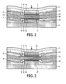
- the piezoelectric switch shown in Figure 1 comprises a housing that is formed by a base plate 1 and a flexible operating plate 2 extending in parallel thereto, which are separated at their edges by two rings or spacers 3, 4.
- Two piezoelectric elements 5, 6 are positioned in the housing, each formed by a carrier 7, or respectively 8, produced out of an electrically conductive material, a piezoelectric crystal 9, 10 and a conductive layer 11, 12 applied thereto.
- Such piezoelectric elements are known per se. With the present invention, they are positioned back to back, in other words with their carriers 7, 8 facing each other.
- the carriers 7, 8 are each connected to a film 13 of electrically insulating material. The edges of this film 13 are clamped into position between the spacers 3, 4. Conductive tracks 15, 16 are mounted on either side of the film 13 and are used to connect the corresponding side of the piezoelectric element 5, 6.
- This piezoelectric switch functions as follows: The switch is operated by pressing the operating plate 2. This causes the center of the plate to move downwards, with the pressure piece 23 being included in this movement. This vertical movement is distributed equally over both piezo elements as a result of the symmetrical structure. Both piezoelectric elements 5, 6 are thus deformed and both crystals 9, 10 generate substantially the same voltage at substantially the same time.
- the elastic suspension of the piezoelectric elements is important to enable the piezoelectric elements to move in the direction of operation. This elastic suspension is achieved by the presence of the elastic films 13, 17 and 18.
- Figure 2 shows a slightly changed configuration, this time in the actuated position.
- an electrically conductive film 37, or respectively 38 is applied instead of an insulating film 17, or respectively 18 on which conductive tracks are mounted.
- an electrically conductive film 35, or respectively 36 is applied to either side of the insulating film 13, fulfilling the function of tracks 15, 16 from an electrical perspective.
- An extra spacer is also added with a ring-shaped air chamber, freeing up space between the piezoelectric elements to bend toward each other.
- FIG. 3 A further slightly changed configuration is shown in Figure 3 .
- film 13 with a round recess between the carriers 7, 8 is replaced by a spacer 33 without any opening, thus obtaining better electrical insulation between the electrical circuits connected to the various piezoelectric crystals.
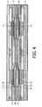
- FIG 4 shows a combination of two switches according to the embodiment of Figure 3 .
- one of the switches is used to compensate the thermal drift of the piezoelectric crystals.
- a crystal in the left switch is connected with opposite polarity and in series to one of the crystals in the right switch. The conductors are therefore connected through to the corresponding films.
- Such a switch is suitable for switching functions on and off, whereby one of the switches is used for switching on the function and the other switch is used for switching off the function in question. From a functional perspective, this prevents the left and right switch from being operated at the same time. However, if such a switching operation does happen, it will not have any consequences.
- a non-operated piezoelectric crystal displays thermal drift in the same way as an operated piezoelectric crystal. If both are connected with opposite polarity and in series, the thermal drift voltages will compensate each other, so that the resultant voltage is independent of the temperature.
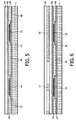
- the switch in question comprises a printed circuit board 41, a flexible operating plate 42 and a spacer 43 positioned between the films 46 and 47.
- Two piezoelectric elements 44 and 45 are arranged inside the switch. The upper side of the piezoelectric elements is connected by conductor 46 and the bottom side of the first piezoelectric element 44 is connected to the electronic circuit via a conductive films 47 on the printed circuit board 41. The bottom side of the second piezoelectric element 45 is connected to the circuit via a conductor 48 on the printed circuit board.
- both piezoelectric crystals are connected in series.
- This embodiment also includes the provision that only one of the piezoelectric elements is operated at any one time.
- Figure 6 shows an embodiment in which only one of the piezoelectric elements, namely element 44, can be operated.
- a spacer body 50 is positioned extending above the non-operable piezoelectric element 45 and a pressure piece 51 is positioned above the operable element.
- the overall structure is covered by a cover plate 52 that is flexible in one direction. This means that the element 45 cannot be operated, so it is always only used as a compensator for the temperature.
Landscapes
- Life Sciences & Earth Sciences (AREA)
- Engineering & Computer Science (AREA)
- Chemical & Material Sciences (AREA)
- Polymers & Plastics (AREA)
- Zoology (AREA)
- Food Science & Technology (AREA)
- Wood Science & Technology (AREA)
- Chemical Kinetics & Catalysis (AREA)
- General Chemical & Material Sciences (AREA)
- Marine Sciences & Fisheries (AREA)
- Health & Medical Sciences (AREA)
- Nutrition Science (AREA)
- Push-Button Switches (AREA)
- Electronic Switches (AREA)
Claims (15)
- Piezoelektrischer Schalter, der folgendes umfasst:- ein Gehäuse;- mindestens ein im Wesentlichen flaches erstes piezoelektrisches Element, das im Gehäuse positioniert ist;- mindestens ein im Wesentlichen flaches zweites piezoelektrisches Element, das im Gehäuse positioniert ist;- eine Betätigungseinheit, die sich zur Hauptebene des ersten piezoelektrischen Elements in transversaler Richtung bewegen kann, um während der Betätigung eine Kraft auf das erste und das zweite piezoelektrische Element auszuüben, wobei diese Kraft das erste und das zweite piezoelektrische Element verformt; und- elektrische Anschlussmittel, die an den gegenüberliegenden Seiten des ersten piezoelektrischen Elements angeschlossen sind, um die vom ersten piezoelektrischen Element erzeugten Signale zu leiten, wenn das erste piezoelektrische Element verformt ist,- elektrische Anschlussmittel, die an den gegenüberliegenden Seiten des zweiten piezoelektrischen Elements angeschlossen sind, um die vom zweiten piezoelektrischen Element erzeugten Signale zu leiten, wenn das zweite piezoelektrische Element verformt ist,dadurch gekennzeichnet, dass die elektrischen Verbindungsmittel eines jeden piezoelektrischen Elements zumindest angrenzend an den Schalter galvanisch voneinander getrennt sind.
- Piezoelektrischer Schalter nach Anspruch 1, dadurch gekennzeichnet, dass das erste piezoelektrische Element mit dem zweiten piezoelektrischen Element im Wesentlichen identisch ist und dass die mechanische Verbindung zwischen der Betätigungseinheit und dem zweiten piezoelektrischen Element so angeordnet ist, dass sie eine Verformung im zweiten piezoelektrischen Element hervorruft, wenn die Betätigungseinheit gedrückt ist, wobei die Verformung im Wesentlichen der des ersten piezoelektrischen Elements gleicht.
- Piezoelektrischer Schalter nach Anspruch 2, dadurch gekennzeichnet, dass das erste und zweite piezoelektrische Element parallel zueinander und in konzentrischer Weise verlaufen.
- Piezoelektrischer Schalter nach Anspruch 3, dadurch gekennzeichnet, dass jedes der piezoelektrischen Elemente einen piezoelektrischen Kristall umfasst, der auf einem Träger positioniert ist, dadurch, dass ein Film an der Seite des Kristalls angebracht ist, die vom Träger weg zeigt und dadurch, dass mindestens der Träger des Kristalls, der dem Betätigungselement am Nächsten liegt, im Gehäuse gelagert ist, so dass es sich in die Richtung bewegen kann, in die sich das Betätigungselement bewegt.
- Piezoelektrischer Schalter nach Anspruch 4, dadurch gekennzeichnet, dass das erste und zweite piezoelektrische Element im Gehäuse mit einander zugewandten Trägern positioniert sind und dadurch, dass beide Träger im Gehäuse gelagert sind, so dass sie sich in die Richtung bewegen können, in die sich das Betätigungselement bewegt.
- Piezoelektrischer Schalter nach Anspruch 5, dadurch gekennzeichnet, dass die Träger auf einem Film befestigt sind, der in die Richtung bewegbar ist, in die sich die Betätigungseinheit bewegt zumindest an der Kante des Trägers und dadurch, dass ein elektrisch isolierender Film zwischen den Trägern angebracht ist, der zumindest über einen Teil der Oberfläche der Träger verläuft, mit elektrisch leitenden Spuren, die auf beiden Seiten des Films aufgebracht sind, wobei die Spuren so angeordnet sind, dass sie als Teil der elektrischen Anschlussmittel wirken.
- Piezoelektrischer Schalter nach Anspruch 6, dadurch gekennzeichnet, dass in den Film Öffnungen eingearbeitet sind.
- Piezoelektrischer Schalter nach Anspruch 6 oder 7, dadurch gekennzeichnet, dass elektrisch isolierender Film an seinen Kanten zwischen zwei Schichten der Seitenwand eines Gehäuses, in dem die Komponenten des Schalters positioniert sind, an Ort und Stelle eingeklemmt ist.
- Piezoelektrischer Schalter nach Anspruch 6, 7 oder 8, dadurch gekennzeichnet, dass der Film, der an der vom Träger abgewandten Seite des Elements angebracht ist, aus elektrisch isolierendem Material hergestellt ist und dass elektrisch leitende Spuren auf diesem Film aufgebracht sind, die so angeordnet sind, dass sie als Teil der elektrischen Anschlusselemente wirken.
- Piezoelektrischer Schalter nach Anspruch 9, dadurch gekennzeichnet, dass zumindest ein drittes piezoelektrisches Element mit gegensätzlicher Polarität angeschlossen und mit dem ersten piezoelektrischen Element in Reihe geschaltet ist und dadurch, dass das erste und dritte piezoelektrische Element zumindest thermisch miteinander verbunden sind.
- Piezoelektrischer Schalter nach Anspruch 10, dadurch gekennzeichnet, dass zumindest ein viertes piezoelektrisches Element mit gegensätzlicher Polarität angeschlossen und mit dem zweiten piezoelektrischen Element in Reihe geschaltet ist und dadurch, dass das zweite und vierte piezoelektrische Element zumindest thermisch miteinander verbunden sind.
- Piezoelektrischer Schalter nach Anspruch 10 oder 11, dadurch gekennzeichnet, dass zumindest eines der Paare aus erstem und drittem piezoelektrischen Element oder beziehungsweise zweitem und viertem piezoelektrischen Element auf einem Träger positioniert ist, der Wärme effektiv leitet.
- Piezoelektrischer Schalter nach Anspruch 12, dadurch gekennzeichnet, dass das dritte und vierte piezoelektrische Element nicht betätigt werden können.
- Piezoelektrischer Schalter nach Anspruch 13, dadurch gekennzeichnet, dass- das dritte und vierte piezoelektrische Element an einer Konstruktion befestigt sind, die der des ersten und zweiten piezoelektrischen Elements entspricht,- das erste, zweite, dritte und vierte piezoelektrische Element jeweils an einen Stromkreis angeschlossen sind, und- der Stromkreis nur geschlossen ist, falls die Kombination aus erstem und zweitem Element oder die Kombination aus drittem und viertem Element betätigt ist.
- Piezoelektrischer Schalter nach einem der vorhergehenden Ansprüche, dadurch gekennzeichnet, dass der Schalter zum Ausführen einer dauerhaften Schaltfunktion angeordnet ist.
Applications Claiming Priority (2)
| Application Number | Priority Date | Filing Date | Title |
|---|---|---|---|
| NL2000026A NL2000026C2 (nl) | 2006-03-14 | 2006-03-14 | Verbeterde piezo-elektrische schakelaar. |
| PCT/NL2007/050101 WO2007105950A1 (en) | 2006-03-14 | 2007-03-13 | Improved piezoelectric switch |
Publications (2)
| Publication Number | Publication Date |
|---|---|
| EP1997228A1 EP1997228A1 (de) | 2008-12-03 |
| EP1997228B1 true EP1997228B1 (de) | 2012-09-19 |
Family
ID=37149404
Family Applications (1)
| Application Number | Title | Priority Date | Filing Date |
|---|---|---|---|
| EP07747347A Active EP1997228B1 (de) | 2006-03-14 | 2007-03-13 | Verbesserter piezoelektrischer schalter |
Country Status (3)
| Country | Link |
|---|---|
| EP (1) | EP1997228B1 (de) |
| NL (1) | NL2000026C2 (de) |
| WO (1) | WO2007105950A1 (de) |
Families Citing this family (9)
| Publication number | Priority date | Publication date | Assignee | Title |
|---|---|---|---|---|
| KR101677334B1 (ko) | 2014-10-24 | 2016-11-17 | 엘지전자 주식회사 | 냉장고 도어 |
| CN105588400B (zh) | 2014-11-07 | 2018-04-13 | Lg电子株式会社 | 冰箱及冰箱控制方法 |
| KR101659181B1 (ko) | 2014-12-22 | 2016-09-30 | 엘지전자 주식회사 | 터치 센서 어셈블리 및 터치 센서 어셈블리가 구비된 냉장고 도어 |
| KR101659180B1 (ko) | 2014-12-22 | 2016-09-22 | 엘지전자 주식회사 | 터치 센서 어셈블리 및 터치 센서 어셈블리가 구비된 냉장고 도어 |
| KR101668922B1 (ko) | 2014-12-24 | 2016-10-24 | 엘지전자 주식회사 | 디스플레이 어셈블리가 구비된 가전제품 및 그 제조 방법 |
| KR101659184B1 (ko) | 2014-12-24 | 2016-09-22 | 엘지전자 주식회사 | 터치 센서 어셈블리 및 터치 센서 어셈블리 제조 방법 |
| KR101668921B1 (ko) | 2014-12-24 | 2016-10-24 | 엘지전자 주식회사 | 터치 센서 어셈블리 및 터치 센서 어셈블리가 구비된 냉장고 도어 |
| KR101639522B1 (ko) | 2015-05-07 | 2016-07-22 | 엘지전자 주식회사 | 터치 센서 어셈블리가 구비된 냉장고 도어 |
| KR101736608B1 (ko) | 2015-11-27 | 2017-05-16 | 엘지전자 주식회사 | 냉장고 |
Family Cites Families (4)
| Publication number | Priority date | Publication date | Assignee | Title |
|---|---|---|---|---|
| DE2125068B2 (de) * | 1971-05-19 | 1977-11-03 | Siemens AG, 1000 Berlin und 8000 München | Tastenbetaetigter signalgeber mit piezokeramischem element fuer fernmelde-, insbesondere fernsprechanlagen |
| US4328441A (en) * | 1980-01-31 | 1982-05-04 | Minnesota Mining And Manufacturing Company | Output circuit for piezoelectric polymer pressure sensor |
| DE19957087B4 (de) * | 1999-11-29 | 2013-07-18 | BROSE SCHLIEßSYSTEME GMBH & CO. KG | Kraftfahrzeug-Türschliesssystem |
| US6466140B1 (en) * | 2000-08-28 | 2002-10-15 | Polara Engineering, Inc. | Pedestrian push button assembly |
-
2006
- 2006-03-14 NL NL2000026A patent/NL2000026C2/nl not_active IP Right Cessation
-
2007
- 2007-03-13 EP EP07747347A patent/EP1997228B1/de active Active
- 2007-03-13 WO PCT/NL2007/050101 patent/WO2007105950A1/en not_active Ceased
Also Published As
| Publication number | Publication date |
|---|---|
| NL2000026C2 (nl) | 2007-09-21 |
| WO2007105950A1 (en) | 2007-09-20 |
| EP1997228A1 (de) | 2008-12-03 |
Similar Documents
| Publication | Publication Date | Title |
|---|---|---|
| EP1997228B1 (de) | Verbesserter piezoelektrischer schalter | |
| CN109256372B (zh) | 具有dc和ac电压端子元件的功率电子子模块及其组件 | |
| CN109786341B (zh) | 具有开关装置的功率半导体模块及其配置 | |
| US8810341B2 (en) | Magnetically actuated micro-electro-mechanical capacitor switches in laminate | |
| US4922070A (en) | Switch assembly | |
| US8576029B2 (en) | MEMS switching array having a substrate arranged to conduct switching current | |
| GB2263813A (en) | Piezoelectric electronic switch | |
| US20160329266A1 (en) | Electronic power device with improved cooling | |
| GB2169747A (en) | Improvements in protective devices for electrical equipment and components, such as capacitors | |
| WO2002005302A1 (en) | El sheet and switch comprising the same | |
| SE432031B (sv) | Piezoelektrisk releanordning | |
| TW200947488A (en) | Slide operation type switch | |
| JP2011216806A (ja) | 電子回路装置 | |
| US4564832A (en) | Membrane keyboard having key closure retention | |
| JP4386767B2 (ja) | 高分子アクチュエータを用いた電気素子 | |
| JP5962746B2 (ja) | 圧電トランス装置 | |
| CN102859629B (zh) | 开关模块系统 | |
| JP3805644B2 (ja) | 圧電アクチュエータ | |
| CN109698412B (zh) | 电跨接元件、电储能器和设备 | |
| TW201250744A (en) | Electro-mechanics switch contact structure | |
| CN107465408B (zh) | 用于致动输入的两件式力传感器输入装置及其生产方法 | |
| TW200421638A (en) | Latching relay with switch bar | |
| KR100846335B1 (ko) | 클릭 스프링 부착 시트 및 이를 사용한 스위치 장치 | |
| JP5113101B2 (ja) | 電気回路の接続構造および電気回路の接続方法 | |
| EP2104588B1 (de) | Verfahren zur vollautomatischen herstellung eines piezoelektrischen schalters und prozess dafür |
Legal Events
| Date | Code | Title | Description |
|---|---|---|---|
| PUAI | Public reference made under article 153(3) epc to a published international application that has entered the european phase |
Free format text: ORIGINAL CODE: 0009012 |
|
| 17P | Request for examination filed |
Effective date: 20080908 |
|
| AK | Designated contracting states |
Kind code of ref document: A1 Designated state(s): AT BE BG CH CY CZ DE DK EE ES FI FR GB GR HU IE IS IT LI LT LU LV MC MT NL PL PT RO SE SI SK TR |
|
| RAP1 | Party data changed (applicant data changed or rights of an application transferred) |
Owner name: AITO INTERACTIVE B.V. |
|
| RIC1 | Information provided on ipc code assigned before grant |
Ipc: H03K 17/965 20060101AFI20091216BHEP |
|
| RAP1 | Party data changed (applicant data changed or rights of an application transferred) |
Owner name: AITO INTERACTIVE B.V. |
|
| GRAP | Despatch of communication of intention to grant a patent |
Free format text: ORIGINAL CODE: EPIDOSNIGR1 |
|
| GRAS | Grant fee paid |
Free format text: ORIGINAL CODE: EPIDOSNIGR3 |
|
| 18D | Application deemed to be withdrawn |
Effective date: 20100721 |
|
| 19U | Interruption of proceedings before grant |
Effective date: 20100831 |
|
| 19W | Proceedings resumed before grant after interruption of proceedings |
Effective date: 20120702 |
|
| D18D | Application deemed to be withdrawn (deleted) | ||
| DAX | Request for extension of the european patent (deleted) | ||
| RAP1 | Party data changed (applicant data changed or rights of an application transferred) |
Owner name: AITO B.V. |
|
| GRAC | Information related to communication of intention to grant a patent modified |
Free format text: ORIGINAL CODE: EPIDOSCIGR1 |
|
| GRAA | (expected) grant |
Free format text: ORIGINAL CODE: 0009210 |
|
| AK | Designated contracting states |
Kind code of ref document: B1 Designated state(s): AT BE BG CH CY CZ DE DK EE ES FI FR GB GR HU IE IS IT LI LT LU LV MC MT NL PL PT RO SE SI SK TR |
|
| REG | Reference to a national code |
Ref country code: CH Ref legal event code: EP |
|
| REG | Reference to a national code |
Ref country code: IE Ref legal event code: FG4D |
|
| REG | Reference to a national code |
Ref country code: AT Ref legal event code: REF Ref document number: 576448 Country of ref document: AT Kind code of ref document: T Effective date: 20121015 |
|
| REG | Reference to a national code |
Ref country code: DE Ref legal event code: R096 Ref document number: 602007025573 Country of ref document: DE Effective date: 20121115 |
|
| PG25 | Lapsed in a contracting state [announced via postgrant information from national office to epo] |
Ref country code: CY Free format text: LAPSE BECAUSE OF FAILURE TO SUBMIT A TRANSLATION OF THE DESCRIPTION OR TO PAY THE FEE WITHIN THE PRESCRIBED TIME-LIMIT Effective date: 20120919 Ref country code: FI Free format text: LAPSE BECAUSE OF FAILURE TO SUBMIT A TRANSLATION OF THE DESCRIPTION OR TO PAY THE FEE WITHIN THE PRESCRIBED TIME-LIMIT Effective date: 20120919 Ref country code: LT Free format text: LAPSE BECAUSE OF FAILURE TO SUBMIT A TRANSLATION OF THE DESCRIPTION OR TO PAY THE FEE WITHIN THE PRESCRIBED TIME-LIMIT Effective date: 20120919 |
|
| REG | Reference to a national code |
Ref country code: NL Ref legal event code: VDEP Effective date: 20120919 |
|
| REG | Reference to a national code |
Ref country code: AT Ref legal event code: MK05 Ref document number: 576448 Country of ref document: AT Kind code of ref document: T Effective date: 20120919 |
|
| REG | Reference to a national code |
Ref country code: LT Ref legal event code: MG4D Effective date: 20120919 |
|
| PG25 | Lapsed in a contracting state [announced via postgrant information from national office to epo] |
Ref country code: SI Free format text: LAPSE BECAUSE OF FAILURE TO SUBMIT A TRANSLATION OF THE DESCRIPTION OR TO PAY THE FEE WITHIN THE PRESCRIBED TIME-LIMIT Effective date: 20120919 Ref country code: GR Free format text: LAPSE BECAUSE OF FAILURE TO SUBMIT A TRANSLATION OF THE DESCRIPTION OR TO PAY THE FEE WITHIN THE PRESCRIBED TIME-LIMIT Effective date: 20121220 Ref country code: SE Free format text: LAPSE BECAUSE OF FAILURE TO SUBMIT A TRANSLATION OF THE DESCRIPTION OR TO PAY THE FEE WITHIN THE PRESCRIBED TIME-LIMIT Effective date: 20120919 Ref country code: LV Free format text: LAPSE BECAUSE OF FAILURE TO SUBMIT A TRANSLATION OF THE DESCRIPTION OR TO PAY THE FEE WITHIN THE PRESCRIBED TIME-LIMIT Effective date: 20120919 |
|
| PG25 | Lapsed in a contracting state [announced via postgrant information from national office to epo] |
Ref country code: CZ Free format text: LAPSE BECAUSE OF FAILURE TO SUBMIT A TRANSLATION OF THE DESCRIPTION OR TO PAY THE FEE WITHIN THE PRESCRIBED TIME-LIMIT Effective date: 20120919 Ref country code: RO Free format text: LAPSE BECAUSE OF FAILURE TO SUBMIT A TRANSLATION OF THE DESCRIPTION OR TO PAY THE FEE WITHIN THE PRESCRIBED TIME-LIMIT Effective date: 20120919 Ref country code: BE Free format text: LAPSE BECAUSE OF FAILURE TO SUBMIT A TRANSLATION OF THE DESCRIPTION OR TO PAY THE FEE WITHIN THE PRESCRIBED TIME-LIMIT Effective date: 20120919 Ref country code: IS Free format text: LAPSE BECAUSE OF FAILURE TO SUBMIT A TRANSLATION OF THE DESCRIPTION OR TO PAY THE FEE WITHIN THE PRESCRIBED TIME-LIMIT Effective date: 20130119 Ref country code: EE Free format text: LAPSE BECAUSE OF FAILURE TO SUBMIT A TRANSLATION OF THE DESCRIPTION OR TO PAY THE FEE WITHIN THE PRESCRIBED TIME-LIMIT Effective date: 20120919 Ref country code: NL Free format text: LAPSE BECAUSE OF FAILURE TO SUBMIT A TRANSLATION OF THE DESCRIPTION OR TO PAY THE FEE WITHIN THE PRESCRIBED TIME-LIMIT Effective date: 20120919 Ref country code: ES Free format text: LAPSE BECAUSE OF FAILURE TO SUBMIT A TRANSLATION OF THE DESCRIPTION OR TO PAY THE FEE WITHIN THE PRESCRIBED TIME-LIMIT Effective date: 20121230 |
|
| PG25 | Lapsed in a contracting state [announced via postgrant information from national office to epo] |
Ref country code: PT Free format text: LAPSE BECAUSE OF FAILURE TO SUBMIT A TRANSLATION OF THE DESCRIPTION OR TO PAY THE FEE WITHIN THE PRESCRIBED TIME-LIMIT Effective date: 20130121 Ref country code: PL Free format text: LAPSE BECAUSE OF FAILURE TO SUBMIT A TRANSLATION OF THE DESCRIPTION OR TO PAY THE FEE WITHIN THE PRESCRIBED TIME-LIMIT Effective date: 20120919 Ref country code: SK Free format text: LAPSE BECAUSE OF FAILURE TO SUBMIT A TRANSLATION OF THE DESCRIPTION OR TO PAY THE FEE WITHIN THE PRESCRIBED TIME-LIMIT Effective date: 20120919 |
|
| PG25 | Lapsed in a contracting state [announced via postgrant information from national office to epo] |
Ref country code: AT Free format text: LAPSE BECAUSE OF FAILURE TO SUBMIT A TRANSLATION OF THE DESCRIPTION OR TO PAY THE FEE WITHIN THE PRESCRIBED TIME-LIMIT Effective date: 20120919 |
|
| PLBE | No opposition filed within time limit |
Free format text: ORIGINAL CODE: 0009261 |
|
| STAA | Information on the status of an ep patent application or granted ep patent |
Free format text: STATUS: NO OPPOSITION FILED WITHIN TIME LIMIT |
|
| PG25 | Lapsed in a contracting state [announced via postgrant information from national office to epo] |
Ref country code: DK Free format text: LAPSE BECAUSE OF FAILURE TO SUBMIT A TRANSLATION OF THE DESCRIPTION OR TO PAY THE FEE WITHIN THE PRESCRIBED TIME-LIMIT Effective date: 20120919 |
|
| 26N | No opposition filed |
Effective date: 20130620 |
|
| PG25 | Lapsed in a contracting state [announced via postgrant information from national office to epo] |
Ref country code: IT Free format text: LAPSE BECAUSE OF FAILURE TO SUBMIT A TRANSLATION OF THE DESCRIPTION OR TO PAY THE FEE WITHIN THE PRESCRIBED TIME-LIMIT Effective date: 20120919 |
|
| REG | Reference to a national code |
Ref country code: DE Ref legal event code: R097 Ref document number: 602007025573 Country of ref document: DE Effective date: 20130620 |
|
| PG25 | Lapsed in a contracting state [announced via postgrant information from national office to epo] |
Ref country code: MC Free format text: LAPSE BECAUSE OF NON-PAYMENT OF DUE FEES Effective date: 20130331 |
|
| REG | Reference to a national code |
Ref country code: CH Ref legal event code: PL |
|
| GBPC | Gb: european patent ceased through non-payment of renewal fee |
Effective date: 20130313 |
|
| REG | Reference to a national code |
Ref country code: IE Ref legal event code: MM4A |
|
| PG25 | Lapsed in a contracting state [announced via postgrant information from national office to epo] |
Ref country code: IE Free format text: LAPSE BECAUSE OF NON-PAYMENT OF DUE FEES Effective date: 20130313 Ref country code: GB Free format text: LAPSE BECAUSE OF NON-PAYMENT OF DUE FEES Effective date: 20130313 Ref country code: LI Free format text: LAPSE BECAUSE OF NON-PAYMENT OF DUE FEES Effective date: 20130331 Ref country code: CH Free format text: LAPSE BECAUSE OF NON-PAYMENT OF DUE FEES Effective date: 20130331 |
|
| PG25 | Lapsed in a contracting state [announced via postgrant information from national office to epo] |
Ref country code: MT Free format text: LAPSE BECAUSE OF FAILURE TO SUBMIT A TRANSLATION OF THE DESCRIPTION OR TO PAY THE FEE WITHIN THE PRESCRIBED TIME-LIMIT Effective date: 20120919 |
|
| PG25 | Lapsed in a contracting state [announced via postgrant information from national office to epo] |
Ref country code: TR Free format text: LAPSE BECAUSE OF FAILURE TO SUBMIT A TRANSLATION OF THE DESCRIPTION OR TO PAY THE FEE WITHIN THE PRESCRIBED TIME-LIMIT Effective date: 20120919 |
|
| PG25 | Lapsed in a contracting state [announced via postgrant information from national office to epo] |
Ref country code: LU Free format text: LAPSE BECAUSE OF NON-PAYMENT OF DUE FEES Effective date: 20130313 Ref country code: BG Free format text: LAPSE BECAUSE OF FAILURE TO SUBMIT A TRANSLATION OF THE DESCRIPTION OR TO PAY THE FEE WITHIN THE PRESCRIBED TIME-LIMIT Effective date: 20120919 Ref country code: HU Free format text: LAPSE BECAUSE OF FAILURE TO SUBMIT A TRANSLATION OF THE DESCRIPTION OR TO PAY THE FEE WITHIN THE PRESCRIBED TIME-LIMIT; INVALID AB INITIO Effective date: 20070313 |
|
| REG | Reference to a national code |
Ref country code: FR Ref legal event code: PLFP Year of fee payment: 10 |
|
| REG | Reference to a national code |
Ref country code: FR Ref legal event code: PLFP Year of fee payment: 11 |
|
| REG | Reference to a national code |
Ref country code: FR Ref legal event code: PLFP Year of fee payment: 12 |
|
| REG | Reference to a national code |
Ref country code: DE Ref legal event code: R082 Ref document number: 602007025573 Country of ref document: DE Representative=s name: MEYER & DOERRING PARTNERSCHAFT MBB PATENTANWAE, DE |
|
| PGFP | Annual fee paid to national office [announced via postgrant information from national office to epo] |
Ref country code: FR Payment date: 20240315 Year of fee payment: 18 |
|
| PGFP | Annual fee paid to national office [announced via postgrant information from national office to epo] |
Ref country code: DE Payment date: 20250218 Year of fee payment: 19 |
|
| PG25 | Lapsed in a contracting state [announced via postgrant information from national office to epo] |
Ref country code: FR Free format text: LAPSE BECAUSE OF NON-PAYMENT OF DUE FEES Effective date: 20250331 |