EP1995759B1 - Mehrpunktspannungs- und Stromsondensystem - Google Patents
Mehrpunktspannungs- und Stromsondensystem Download PDFInfo
- Publication number
- EP1995759B1 EP1995759B1 EP07253937.2A EP07253937A EP1995759B1 EP 1995759 B1 EP1995759 B1 EP 1995759B1 EP 07253937 A EP07253937 A EP 07253937A EP 1995759 B1 EP1995759 B1 EP 1995759B1
- Authority
- EP
- European Patent Office
- Prior art keywords
- signals
- signal
- output
- module
- power
- Prior art date
- Legal status (The legal status is an assumption and is not a legal conclusion. Google has not performed a legal analysis and makes no representation as to the accuracy of the status listed.)
- Ceased
Links
Images


Classifications
-
- H—ELECTRICITY
- H01—ELECTRIC ELEMENTS
- H01J—ELECTRIC DISCHARGE TUBES OR DISCHARGE LAMPS
- H01J37/00—Discharge tubes with provision for introducing objects or material to be exposed to the discharge, e.g. for the purpose of examination or processing thereof
- H01J37/32—Gas-filled discharge tubes
- H01J37/32917—Plasma diagnostics
- H01J37/32935—Monitoring and controlling tubes by information coming from the object and/or discharge
-
- H—ELECTRICITY
- H01—ELECTRIC ELEMENTS
- H01J—ELECTRIC DISCHARGE TUBES OR DISCHARGE LAMPS
- H01J37/00—Discharge tubes with provision for introducing objects or material to be exposed to the discharge, e.g. for the purpose of examination or processing thereof
- H01J37/32—Gas-filled discharge tubes
- H01J37/32009—Arrangements for generation of plasma specially adapted for examination or treatment of objects, e.g. plasma sources
- H01J37/32082—Radio frequency generated discharge
- H01J37/32174—Circuits specially adapted for controlling the RF discharge
-
- H—ELECTRICITY
- H04—ELECTRIC COMMUNICATION TECHNIQUE
- H04B—TRANSMISSION
- H04B17/00—Monitoring; Testing
- H04B17/30—Monitoring; Testing of propagation channels
- H04B17/309—Measuring or estimating channel quality parameters
- H04B17/318—Received signal strength
Definitions
- the present disclosure relates to metrology for sensing radio frequency power, particularly but not entirely in plasma processing systems.
- RF plasma radio frequency
- CDs compact disks
- DVDs digital versatile discs
- RF plasma process is monitored and controlled by a closed loop control system.
- RF plasma control systems measure one or more parameters of RF power that is applied to a plasma chamber.
- a plasma controller repeatedly adjusts the parameters based on the measurements and a control algorithm.
- the measurements are taken at more than one location in the RF power path and it can be challenging to synchronize or time-correlate the measurements from the various locations.
- Radio communication sites may include radio transmitters, receivers, antennas, and the like. They may also include test and/or monitoring equipment to ensure that the radio communication sites are functioning properly and in accordance with government regulations and/or industry standards.
- the test and/or monitoring equipment can measure RF system parameters at more than one location in the RF path of a particular station. While the parameters may be used to ensure the system is functioning properly, it can be challenging to synchronize or time-correlate the parameter measurements from the various locations.
- US 2006/232471 discloses phase and frequency control of a radio frequency generator from an external source.
- US 2006/249729 discloses a sensor apparatus for measuring a plasma process parameter.
- US 5939886 discloses a plasma monitoring and control method and system.
- US 2006/239389 discloses a system for detecting and correcting for spurious frequencies that may coincide in a bandwidth of interest in an RF metrology system.
- US 2004/065539 Sosnowski Janusz [US] discloses a method and apparatus for maintaining a plasma in a plasma region.
- WO 2004/008502 discloses an RF generator for use in an RF plasma system.
- EP1244133 discloses A radio frequency (RF) probe analysis system having a broadband design.
- US 2004/007326 discloses a wafer probe for measuring plasma and surface characteristics in plasma processing environments.
- a metrology system for monitoring radio frequency (RF) power at a plurality of locations in a circuit, comprising: a plurality of RF sensors that each generate a respective analog signal based on electrical properties of the RF power output by respective RF generators; a multiplexing module that receives the signal from each of the RF sensors and generates an output signal based on the signals received from each of the RF sensors; an analysis module that generates messages based on the output signal, wherein the messages contain information regarding the electrical properties that are sensed by the plurality of RF sensors; and a control module for generating control signals for the RF generators in accordance with the information output by the analysis module.
- RF radio frequency
- a metrology system for monitoring radio frequency (RF) power at a plurality of locations in a circuit.
- the system includes a plurality of sense channels that each generate an output signal based on an electrical property of the RF power at one of the locations in the circuit.
- Each sense channel includes a RF sensor that generates a first signal based on the electrical property of the RF power, an oscillator that generates a periodic signal, and a mixer that mixes the first signal with the periodic signal to generate the output signal for the sense channel.
- a RF combiner generates a second output signal based on the plurality of output signals from the sense channels.
- a metrology system for monitoring radio frequency (RF) power at a plurality of locations in a circuit
- the system includes a plurality of sense channels that each generate a pair of output signals based on electrical properties of the RF power at one of the locations in the circuit.
- Each sense channel includes a RF sensor that generates a pair of analog signals based on the RF power, an oscillator that generates first and second periodic signals that are out-of-phase, a first mixer that mixes the first periodic signal with one of the analog signals to generate one of the output signals of the sense channel, and a second mixer that mixes the second periodic signal with the other one of the analog signals to generate a second one of the output signals of the sense channel.
- a first RF combiner generates a first broadband signal based on the plurality of output signals from the first mixers and a second RF combiner generates a second broadband signal based on the plurality of output signals from the second mixers.
- a metrology system for monitoring radio frequency (RF) power at a plurality of locations in a circuit.
- the system includes a plurality of RF sensors that each generates a pair of analog signals based on electrical properties of the RF power at one of the locations in the circuit, a first multiplexer that receives one of the analog signals from each pair of analog signals and routes one of the received signals to an output of the first multiplexer in accordance with a control signal, a second multiplexer that receives the other one of the analog signals from each pair of analog signals and routes one of the received signals to an output of the second multiplexer in accordance with the control signal, and an analysis module that generates messages based on the signals from the output of the first and second multiplexers.
- the messages contain information regarding the electrical properties that are sensed by the plurality of sense channels.
- a method for monitoring radio frequency (RF) power at a plurality of locations in a circuit includes generating an output signal based on an electrical property of the RF power at an associated one of the locations in the circuit, each generating step including generating a first signal based on the RF power, generating a periodic signal, and mixing the first signal with the periodic signal to generate the output signal.
- the method includes combining the output signals to generate a broadband signal that includes frequency components of each of the output signals.
- a method for monitoring radio frequency (RF) power at a plurality of locations in a circuit includes generating a pair of analog signals based on electrical properties of the RF power at an associated one of the locations in the circuit, multiplexing one signal of the pair of analog signals to a first output signal, multiplexing the other one of the signals of the pair of analog signals to a second output signal, and generating messages based on the signals from the first and second output signals of the multiplexing steps.
- the messages contain information regarding the electrical properties that are sensed by the plurality of sense channels.
- module refers to an Application Specific Integrated Circuit (ASIC), an electronic circuit, a processor (shared, dedicated, or group) and memory that execute one or more software or firmware programs, a combinational logic circuit, and/or other suitable components that provide the described functionality.
- ASIC Application Specific Integrated Circuit
- processor shared, dedicated, or group
- memory that execute one or more software or firmware programs, a combinational logic circuit, and/or other suitable components that provide the described functionality.
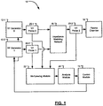
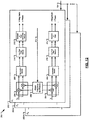
- RF plasma generator 10 includes a multiplexing module 22 that facilitates measuring RF power at a plurality of locations within RF plasma generator 10. Multiplexing module 22 is described below in more detail.
- RF plasma generator 10 includes RF generators 12-1 and 12-2, collectively referred to as RF generators 12.
- a control module 14 generates control signals for RF generators 12.
- the control signals determine electrical parameters, such as voltage, current, power, and the like, of the RF power at the outputs of RF generators 12.
- the outputs of RF generators 12 communicate with respective inputs of an impedance matching network 16.
- Impedance matching network 16 matches an input impedance of a plasma chamber 18 to an output impedance of RF generators 12, which is typically 50 ohms.
- RF plasma generator 10 includes a plurality of sensors or probes 20 that sense one or more parameters of the RF power at the various locations.
- First and second probes 20-1 and 20-2 sense the RF power at the outputs of respective ones of RF generators 12.
- a third probe 20-3 senses the RF power between the output of impedance matching network 16 and the input of plasma chamber 18.
- Each probe 20 generates one or more signals that represent the electrical parameter or parameters of interest.
- probes 20 can be directional couplers when the parameters of interest are forward and/or reflected power.
- Probes 20 can be voltage/current (V/I) probes when the parameters of interest are voltage and/or current.
- the signals from probes 20 communicate with inputs of multiplexing module 22.
- Multiplexing module 22 shifts the frequency of and/or samples the signals and communicates the results of the frequency shift and/or sampling to an analysis module 24.
- Analysis module 24 generates data based on the results. The data quantifies the parameters of interest as sensed by respective ones of probes 20. Analysis module 24 generates one or more digital and or analog signals that communicate the data and/or information to control module 14. Control module 14 then adjusts the control signals based on the data and a control algorithm.
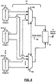
- RF plasma generator 10 is shown with a multiple shower head plasma chamber 18'.
- the RF power at the output of impedance matching network 16 communicates with an input of a splitter 26.
- Splitter 26 divides or splits the RF power to the plurality of inputs of plasma chamber 18'.
- Probes 20-3, 20-4, and 20-5 sense the RF power that is applied to respective ones of the inputs of plasma chamber 18'.
- Multiplexing module 22 receives and processes the signals from additional probes 20-4 and 20-5 and includes their information in the signal or signals communicated to analysis module 24.
- Wireless RF transmitter 50 employs multiplexing module 22 and a plurality of probes 20 that sense the RF power at various locations within wireless RF transmitter 50.
- Wireless RF transmitter 50 includes a plurality of RF generators or transmitters 52-1, 52-2, and 52-3 that generate RF signals.
- the RF signals communicate with respective inputs of a RF filter/combiner 54.
- RF filter/combiner 54 passes the fundamental frequency of the RF signals and combines them to form a composite output RF signal.
- the composite output RF signal communicates with an input of an antenna 56.
- Probes 20-1, ..., 20-4 sense the RF power at their respective locations.
- Multiplexing module 22 receives and processes the signals from probes 20-1, ..., 20-4.
- Multiplexing module 22 combines and/or samples the signals and communicates the results of the combination and/or sampling to analysis module 24.
- Analysis module 24 generates data based on the results. The data quantifies the parameters of interest as sensed by respective ones of probes 20.
- Analysis module 24 communicates the data to control module 14.
- Control module 14 then adjusts control signals based on the data and a control algorithm. The control signals feed back to RF transmitters 52 and vary one or more parameters of their respective RF power outputs.
- FIG. 4 shows probes 20 as V/I probes that generate signals that represent the voltage and current of the RF power at the respective probe. It should be appreciated that probes 20 may in some embodiments be implemented as directional couplers that generate signals that represent the forward and reflected powers of the RF power at the respective probe. Probes 20 may also be any other type of probe that generates signals based on selected electrical properties of interest.
- probes 20 may down convert the frequency of the sensed signal.
- An example of such probes 20 is shown in U.S Patent 5,770,922 , which is hereby included by reference in its entirety.
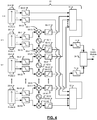
- Multiplexing module 22 includes a plurality of mixing modules 60-1, 60-2, ..., 60-N that receive the signals from respective ones of probes 20-1, 20-2, ..., 20-N.
- Each mixing module 60 includes a respective local oscillator 62 and pair of mixers 64.
- Each pair of mixers 64 receives respective in-phase and out-of-phase, e.g. sine and cosine, signals from their associated local oscillator 62.
- Each of local oscillators 62 may have a different frequency from the others.
- the frequencies of local oscillators 62 can be less than or greater than a first signal frequency of the signals from probes 20. In some embodiments, such as when the frequencies of the signals from probes 20 are different, local oscillators 62 can use a common frequency.
- the signals from first probe 20-1 may remain at their fundamental frequency and do not need to pass through a mixing module 60.
- the signals from probes 20 may pass through respective low-pass filters 66.
- the signals from mixers 64-2
- a first RF combiner 70 receives the signals from the first mixers 64-11, 64-21, ..., 64-N1 in each of mixing modules 60.
- a second RF combiner 72 receives the signals from the second mixers 64-12, 64-22, ..., 64-N2 in each mixing modules 60.
- Outputs of RF combiners 70 and 72 communicate with the inputs of controller 14.
- the outputs of RF combiners 70 and 72 may pass through respective low-pass filters 74 and 76 before they communicate with the inputs of controller 14.
- one or more of filters 66, 68, 74 and 76 may include an associated scaling module. Gains of the scaling modules may be adjusted so that amplitudes of the signals of interest are matched with the dynamic range of the inputs to analysis module 24.
- Mixing modules 60 shift the signals from respective probes 20 in the frequency domain before the signals are applied to analysis module 24. Mixing modules 60 thereby allow analysis module 24 to simultaneously receive information from all probes 20. Analysis module 24 should have an input bandwidth that accommodates desired portions of the frequency spectrums of the signals, filtered or unfiltered, at the outputs of mixers 64 and probe 20-0. Such analysis modules 24 are presently manufactured by MKS Instruments with part numbers VIP2001, VIP2007, and VIP2009. US Patents 6,522,121 and 6,707,255 are included herein by reference in their entirety and also provide examples of analysis modules 24 that are compatible with the frequency-division version of multiplexing module 22.
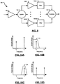
- a spectral diagram 100 shows, by way of non-limiting example, frequency components of the analog signals from four probes 20 prior to being applied to respective mixing modules 60.
- Spectral diagram 100 shows that the frequency components of the signals from probes 20 lie on top of each other. If these signals were applied directly to analysis module 24 (e.g. without passing through mixing modules 60) then analysis module 24 would not be able to discern which signals are associated with which probes 20.
- a spectral diagram 120 shows frequency components of the signals at the outputs of four mixing modules 60.
- Spectral diagram 120 assumes that the frequencies of local oscillators 62 are less than the fundamental frequency of the signals from probes 20. Each set of signals at a particular magnitude is associated with one of probes 20.
- Spectral diagram 120 shows that mixing modules 60 shift the fundamental frequencies of the signals from probes 20 to manage overlap of the frequency components each signal. Mixing modules 60 thereby enable analysis module 24 to discern which frequency components are associated with a particular probe 20.
- the frequency shifts of the signals from each probe 20 vary in accordance with the frequency of the associated local oscillator 62 and, in some embodiments, are equal to +/- the frequency of the associated local oscillator 62. It should be appreciated by those skilled in the art that when filters 66, 68, 74, and/or 76 are used they remove some of the frequency components from the signals that are generated by probes 20.
- a spectral diagram 130 shows frequency components of the signals at the outputs of four mixing modules 60.
- Spectral diagram 130 assumes that the frequencies of local oscillators 62 are greater than the fundamental frequency of the signals from probes 20.
- Each set of signals at a particular magnitude is associated with one of probes 20.
- Spectral diagram 130 shows that mixing modules 60 shift the fundamental frequencies of the signals from probes 20 to manage the overlap of frequency components of each signal.
- the frequency components of each probe 20 are grouped together within a corresponding frequency band. The grouped frequencies enable analysis module 24 to discern which frequency components are associated with a particular probe 20.
- the frequency shifts of the signals from each probe 20 vary in accordance with the frequency of the associated local oscillator 62 and, in some embodiments, are equal to +/- the frequency of the associated local oscillator 62. It should be appreciated by those skilled in the art that when filters 66, 68, 74, and/or 76 are used they remove some of the frequency components from the signals that are generated by probes 20.
- the time-division multiplexing module 22 allows the full frequency spectrum from one of probes 20 to reach analysis module 24 at any selected time.
- a first multiplexer 150 includes a plurality of inputs that receives one of the analog signals from each of probes 20.
- a second multiplexer 152 includes a plurality of inputs that receive the second analog signals from each of probes 20.
- Each of multiplexers 150 and 152 include an input that receives a probe select signal 154.
- Probe select signal 154 determines which probe 20 has its signals routed to the outputs of multiplexers 150 and 152 at the selected time.
- a signal conditioning and partitioning module 160 is shown.
- One or more signal conditioning and partitioning modules 160 are employed when multiplexing module 22 of FIG. 8 is employed with multiple RF generators 12, such as shown in FIGs. 1-3 .
- RF generators 12 employ different fundamental frequencies. The fundamental frequencies can be combined in at least one of impedance matching network 16 and RF filter/combiner 54.
- Signal conditioning and partitioning module 160 matches the bandwidth and gain of the RF signal from a respective one of probes 20 with dynamic range of analysis module 24.
- Each signal conditioning and partitioning module 160 receives the signal from a respective output of one of probes 20.
- a scaling module 162 amplifies or attenuates the signal before it reaches an input of a 1-to-M splitter 164, where M is a number of frequency bands.
- Each output of 1-to-M splitter 164 provides a duplicate of the signal that is applied to the input.
- Each of the M outputs communicates with a respective one of M scaling modules 166.
- Each scaling module 166 can have a gain that is less than, equal to, or greater than unity.
- the outputs of scaling modules 166 communicate with respective inputs of filters 168. Passbands of filters 168 may be selected based on frequencies of interest to the user.
- a combiner 170 combines output signals from filters 168.
- An output of combiner 170 provides a filtered sensor signal that is communicated to a respective input of multiplexer 150 or multiplexer 152.
- the gains of scaling modules 162 and 166 and the cutoff frequencies and bandwidths of filters 168 may be selected based on the M different frequency bands and to maximize quantization of the RF signal by analysis module 24.
- Each filter 168 may be implemented as an all pass, a low pass, a high pass, or a band pass filter.
- FIG. 10A shows a spectral diagram at the input of scaling module 162. It can be seen that the amplitudes of f 0 and f 1 can be unequal and not necessarily matched to an input characteristic or limitation of analysis module 24.
- FIG. 10B shows the spectral diagram at the output of filter 168-1.
- FIG. 10B assumes that filter 168-1 is implemented as a low-pass filter with a cutoff frequency greater than f 0 and less than f 1 .
- a passband of filter 168-1 is shown at 172.
- FIG. 10C shows the spectral diagram at the output of filter 168-M.
- FIG. 10C assumes that filter 168-M is implemented as a bandpass filter with a center frequency at f 1 and a lower cutoff frequency greater than f 0 .
- a passband of filter 168-M is shown at 174.
- FIG. 10C also assumes that the gain of scaling module 166-M is less than unity, thereby reducing the amplitude of f 1 prior to entering combiner 170.
- FIG. 10D shows the spectral diagram at the output of combiner 170.
- FIG. 11 a functional block diagram is shown of one of various architectures of analysis module 24 that may be employed with the time-division version of multiplexing module 22 ( FIG. 8 ).
- the inputs V and I each receive a signal from a respective signal conditioning and partitioning module 160.
- Each input signal is applied to a respective low pass filter 180 and a respective high pass filter 182.
- filters 180 and 182 may be omitted and the filtering function be satisfied by filters 168.
- a first pair of analog-to-digital (A/D) converters 184 convert low frequency components of the respective V and I signals from filters 180.
- a second pair of A/D converters 186 convert high frequency components of the respective V and I signals from filters 182.
- A/D converter pair 184 communicates the converted signals to a field programmable gate array (FPGA) 188.
- A/D converter pair 186 communicates the converted signals to a field programmable gate array (FPGA) 190.
- Each FPGA 188 and 190 converts its respective digitized voltage and current data into in-phase (I) and quadrature (Q) signals.
- a digital signal processor (DSP) 192 quantifies parameters of interest based on the I and Q signals from FPGAs 188 and 190.
- a block diagram 200 shows functionality that is provided by FPGA 188 and DSP 192. It should be appreciated by those skilled in the art that the functions shown in block diagram 200 may also be provided by other means at a user's discretion.
- Block diagram 200 includes N conversion modules 202-1, ..., 202-N, which are collectively referred to as conversion modules 202.
- Each conversion module 202 is associated with one of probes 20 and receives the converted data from one of A/D converter pairs 184 and 186.
- Probe select signal 154 (also shown in FIG. 8 ) activates the conversion module 202 that is associated with the selected one of probes 20.
- Each conversion module 202 includes a pair of mixing modules 204.
- Mixing modules 204 receive digital signals acquired from the associated one of A/D converter pairs184, 186.
- Each mixing module 204 also receives two inputs from a digital frequency synthesizer 206.
- digital frequency synthesizer 206 generates digital mixing signals.
- digital frequency synthesizer 206 produces sine and cosine waveforms that correspond with one or more of the frequencies of interest from the associated signal conditioning and partitioning module 160.
- a frequency set point signal 214 establishes the operating frequency of digital frequency synthesizer 206.
- the frequency set point signal can be switched through a plurality of setpoints to process a plurality of the frequencies of interest for a particular probe 20.
- the frequency setpoints are a frequency offset received from frequency sources that drives the RF generators 12 or transmitters 52.
- Each digital mixing module 204 combines digital mixing signals received from digital frequency synthesizer 206 with the conversion data received from the associated A/D converter pair. To do so, each digital mixing module 204 includes two digital multipliers. In addition, digital mixing modules 204 operate at the sample rate of the associated A/D converter pair. The result from each digital mixing module 204 is a spectrum constructed from the sum and difference of the frequencies contained in the digitized data and the signals provided by the digital frequency synthesizer.
- Outputs of mixer modules 204 communicate with inputs of respective decimation modules 208.
- Decimation modules 208 translate the sample rate to a lower or baseband data rate.
- decimation is described in U.S. Patent 6,707,255 , which is hereby incorporated by reference in its entirety.
- mixing modules 204 and decimation modules 208 are implemented with FPGAs 188 and 190.
- Outputs of decimation modules 208 communicate with inputs of respective low pass filter modules 210.
- Low pass filter modules 210 shape the spectral output of decimation modules 208.
- Outputs of low pass filter modules 210 communicate with respective Cartesian to polar conversion modules 212.
- Conversion modules 212 convert the filtered data from low pass filter modules 210 to a polar coordinate system.
- low pass filter modules 210 and Cartesian to polar conversion modules 212- are implemented with DSP 192.
- a metrology system monitors radio frequency (RF) power at a plurality of locations in a circuit.
- the system includes a plurality of RF sensors that generate respective analog signals based on electrical properties of the RF power, a multiplexing module that generates an output signal based on the analog signals, and an analysis module that generates messages based on the output signal.
- the messages contain information regarding the electrical properties that are sensed by the plurality of RF sensors.
Landscapes
- Engineering & Computer Science (AREA)
- Physics & Mathematics (AREA)
- Plasma & Fusion (AREA)
- Analytical Chemistry (AREA)
- Chemical & Material Sciences (AREA)
- Electromagnetism (AREA)
- Signal Processing (AREA)
- Computer Networks & Wireless Communication (AREA)
- Quality & Reliability (AREA)
- Plasma Technology (AREA)
- Transmitters (AREA)
- Drying Of Semiconductors (AREA)
- Measurement Of Current Or Voltage (AREA)
- Arrangements For Transmission Of Measured Signals (AREA)
Claims (26)
- Metrologiesystem zum Überwachen von Radiofrequenz-(RF)-Leistung an einer Mehrzahl von Stellen in einem Kreislauf, das Folgendes umfasst:eine Mehrzahl von RF-Sensoren (20-1, 20-2), die jeweils ein jeweiliges Analogsignal auf der Basis von elektrischen Eigenschaften des RF-Leistungsausgangs durch jeweilige RF-Generatoren (12-1, 12-2) erzeugen;ein Multiplexiermodul (22), das das Signal von jedem der RF-Sensoren empfängt und ein Ausgangssignal auf der Basis der von jedem der RF-Sensoren empfangenen Signale erzeugt;ein Analysemodul (24), das Nachrichten auf der Basis des Ausgangssignals erzeugt, wobei die Nachrichten Informationen über die elektrischen Eigenschaften enthalten, die von der Mehrzahl von RF-Sensoren (20) erfasst werden; undein Steuermodul (14) zum Erzeugen von Steuersignalen für die RF-Generatoren (12-1, 12-2) gemäß den von dem Analysemodul (24) ausgegebenen Informationen.
- Metrologiesystem nach Anspruch 1, wobei das Multiplexiermodul (22) Zeitmultiplexierung zum Multiplexen der Signale zum Ausgangssignal nutzt.
- Metrologiesystem nach Anspruch 1 oder Anspruch 2, wobei das Multiplexiermodul (22) Frequenzmultiplexierung zum Multiplexen der Signale zum Ausgangssignal nutzt.
- Metrologiesystem nach Anspruch 1, wobei jeder RF-Sensor (20-1, 20-2) ein Paar Analogsignale auf der Basis von elektrischen Eigenschaften der RF-Leistung an einer der Stellen in dem Kreislauf erzeugt;
wobei das Multiplexiermodul (22) einen ersten Multiplexer (150) umfasst, der eines der Analogsignale von jedem Paar Analogsignalen empfängt und eines der empfangenen Signale zu einem Ausgang des ersten Multiplexers (150) gemäß einem Steuersignal leitet;
einen zweiten Multiplexer (152), der das andere der Analogsignale von jedem Paar Analogsignalen empfängt und eines der empfangenen Signale zu einem Ausgang des zweiten Multiplexers (152) gemäß dem Steuersignal leitet;
wobei das Analysemodul (24) zum Erzeugen von Nachrichten auf der Basis der Signale vom Ausgang des ersten und zweiten Multiplexers (150, 152) konfiguriert ist, wobei die Nachrichten Informationen über die elektrischen Eigenschaften enthalten. - Metrologiesystem nach Anspruch 4, das ferner eine Mehrzahl von Signalkonditionierungs- und - partitionierungsmodulen (160) umfasst, die in Serie mit jeweiligen der Analogsignale von den RF-Sensoren (20-1, 20-2) geschaltet sind, wobei jedes Signalkonditionierungsmodul Folgendes umfasst:eine Mehrzahl von Filtern (168), die jeweilige Frequenzkomponenten des assoziierten einen der Analogsignale durchlassen;eine Mehrzahl von Skalierungsmodulen (166), die wenigstens einen Teil der Frequenzkomponenten verstärken oder dämpfen; undeinen Kombinator (170), der die Frequenzkomponenten kombiniert, um das Signal zu erzeugen, das zum ersten oder zweiten Multiplexer (150, 152) übermittelt wird.
- Metrologiesystem nach Anspruch 4, wobei das Analysemodul (24) ferner Filter umfasst, die jeweilige Signale von Ausgängen des ersten und zweiten Multiplexers (150, 152) filtern.
- Metrologiesystem nach Anspruch 6, das ferner ein Paar Analog-Digital-Wandler (184, 186) umfasst, die jeweilige Signale vom ersten und zweiten Multiplexer (150, 152) umwandeln.
- Metrologiesystem nach Anspruch 7, wobei das Analysemodul (24) ferner eine Mehrzahl von Wandlungsmodulen (202) umfasst, die die Signale von den Multiplexern (150, 152) in eine Basisbandfrequenz umwandeln, die niedriger ist als eine Frequenz der RF-Leistung.
- Metrologiesystem nach Anspruch 8, wobei jedes Umwandlungsmodul (202) Mischermodule (204) beinhaltet, die umgewandelte Signale von dem Paar Analog-Digital-Wandler (184, 186) mischen.
- Metrologiesystem nach Anspruch 9, das ferner Dezimierungsmodule (208) umfasst, die Ausgangssignale von jeweiligen der Mischer-Module (204) dezimieren.
- Metrologiesystem nach Anspruch 10, das ferner Tiefpassfiltermodule (210) umfasst, die Ausgangssignale von jeweiligen der Dezimierungsmodule (208) filtern.
- Metrologiesystem nach Anspruch 1, das ferner für jeden RF-Sensor (20) einen Oszillator (62) umfasst, der ein periodisches Signal erzeugt, wobei das Multiplexiermodul (22) ein Mischer-Modul (60), das das Signal mit dem periodischen Signal mischt, und ein RF-Kombinatormodul (70, 72) umfasst, das das Ausgangssignal erzeugt.
- Metrologiesystem nach Anspruch 1, wobei die RF-Sensoren (20-1, 20-2) direktionale Koppler sind.
- Metrologiesystem nach Anspruch 1, wobei die RF-Sensoren (20-1, 20-2) Spannungs/Strom-(V/I)-Sonden sind.
- Verfahren zum Überwachen von Radiofrequenz-(RF)-Leistung an einer Mehrzahl von Stellen in einem Kreislauf, das Folgendes beinhaltet:Erzeugen eines Paares von Analogsignalen auf der Basis von elektrischen Eigenschaften des RF-Leistungsausgangs durch jeweilige RF-Generatoren (12-1, 12-2);Erzeugen eines gemultiplexten Ausgangssignals auf der Basis der von jedem jeweiligen RF-Generator ausgegebenen Signale;Erzeugen von Nachrichten auf der Basis des Signals, wobei die Nachrichten Informationen über die elektrischen Eigenschaften enthalten, die von der Mehrzahl von RF-Sensoren (20-1, 20-2) erfasst werden; undSteuern der RF-Leistungsgeneratoren (12-1, 12-2) gemäß den Nachrichten.
- Verfahren nach Anspruch 15, Erzeugen eines Paares der genannten Signale auf der Basis von elektrischen Eigenschaften der RF-Leistung an einer assoziierten einen der Stellen in dem Kreislauf;
Multiplexen von einem Signal des Paares von Signalen zu einem erstem genannten Ausgangssignal;
Multiplexen des anderen der Signale des Paares von Signalen zu einem anderen genannten Ausgangssignal; und
Erzeugen der genannten Nachrichten auf der Basis der Signale von den ersten und zweiten Ausgangssignalen der Multiplexierschritte. - Verfahren nach Anspruch 16, das ferner Folgendes beinhaltet:Filtern jedes aus dem Paar von Signalen in eine Mehrzahl von jeweiligen Frequenzkomponenten;Verstärken wenigstens eines Teils der Frequenzkomponenten; undKombinieren der Frequenzkomponenten zum Erzeugen von jeweiligen Signalen in dem Paar von Signalen, die zum ersten oder zweiten Multiplexer (150, 152) übermittelt werden.
- Verfahren nach Anspruch 17, das ferner das Filtern von jeweiligen ersten und zweiten Ausgangssignalen beinhaltet.
- Verfahren nach Anspruch 18, das ferner das Digitalisieren von jeweiligen ersten und zweiten Ausgangssignalen beinhaltet.
- Verfahren nach Anspruch 19, das ferner das Umwandeln der Ausgangssignale in eine Basisbandfrequenz beinhaltet, die niedriger ist als eine Frequenz der RF-Leistung.
- Verfahren nach Anspruch 20, das ferner das Mischen des digitalisierten Signals mit einem digitalen Signal beinhaltet.
- Verfahren nach Anspruch 21, das ferner das Dezimieren der Ausgangssignale beinhaltet.
- Verfahren nach Anspruch 22, das ferner das Filtern der dezimierten Signale beinhaltet.
- Verfahren nach Anspruch 15, das ferner das Bereitstellen eines periodischen Signals für jedes genannte Signal beinhaltet, wobei das gemultiplexte Ausgangssignal durch Mischen der Signale mit dem periodischen Signal und Kombinieren der gemischten Signale erzeugt wird.
- Verfahren nach Anspruch 15, wobei die elektrische Eigenschaft Vorwärtsleistung und/oder reflektierte Leistung beinhaltet.
- Verfahren nach Anspruch 15, wobei die elektrische Eigenschaft Spannung und/oder Strom beinhaltet.
Priority Applications (1)
| Application Number | Priority Date | Filing Date | Title |
|---|---|---|---|
| EP18199675.2A EP3483917B1 (de) | 2007-03-14 | 2007-10-04 | Mehrpunktspannungs- und stromsondensystem |
Applications Claiming Priority (2)
| Application Number | Priority Date | Filing Date | Title |
|---|---|---|---|
| US89473807P | 2007-03-14 | 2007-03-14 | |
| US11/763,298 US8055203B2 (en) | 2007-03-14 | 2007-06-14 | Multipoint voltage and current probe system |
Related Child Applications (2)
| Application Number | Title | Priority Date | Filing Date |
|---|---|---|---|
| EP18199675.2A Division EP3483917B1 (de) | 2007-03-14 | 2007-10-04 | Mehrpunktspannungs- und stromsondensystem |
| EP18199675.2A Division-Into EP3483917B1 (de) | 2007-03-14 | 2007-10-04 | Mehrpunktspannungs- und stromsondensystem |
Publications (4)
| Publication Number | Publication Date |
|---|---|
| EP1995759A2 EP1995759A2 (de) | 2008-11-26 |
| EP1995759A3 EP1995759A3 (de) | 2010-07-07 |
| EP1995759B1 true EP1995759B1 (de) | 2018-12-12 |
| EP1995759B8 EP1995759B8 (de) | 2019-02-27 |
Family
ID=64051265
Family Applications (2)
| Application Number | Title | Priority Date | Filing Date |
|---|---|---|---|
| EP07253937.2A Ceased EP1995759B8 (de) | 2007-03-14 | 2007-10-04 | Mehrpunktspannungs- und Stromsondensystem |
| EP18199675.2A Ceased EP3483917B1 (de) | 2007-03-14 | 2007-10-04 | Mehrpunktspannungs- und stromsondensystem |
Family Applications After (1)
| Application Number | Title | Priority Date | Filing Date |
|---|---|---|---|
| EP18199675.2A Ceased EP3483917B1 (de) | 2007-03-14 | 2007-10-04 | Mehrpunktspannungs- und stromsondensystem |
Country Status (5)
| Country | Link |
|---|---|
| US (2) | US8055203B2 (de) |
| EP (2) | EP1995759B8 (de) |
| JP (2) | JP5378678B2 (de) |
| CN (1) | CN101267707B (de) |
| TW (1) | TWI467941B (de) |
Families Citing this family (44)
| Publication number | Priority date | Publication date | Assignee | Title |
|---|---|---|---|---|
| US8055203B2 (en) * | 2007-03-14 | 2011-11-08 | Mks Instruments, Inc. | Multipoint voltage and current probe system |
| US7970562B2 (en) | 2008-05-07 | 2011-06-28 | Advanced Energy Industries, Inc. | System, method, and apparatus for monitoring power |
| GB0823565D0 (en) * | 2008-12-24 | 2009-01-28 | Oxford Instr Plasma Technology | Signal generating system |
| US8040068B2 (en) * | 2009-02-05 | 2011-10-18 | Mks Instruments, Inc. | Radio frequency power control system |
| CN102473631B (zh) * | 2009-06-30 | 2014-11-26 | 朗姆研究公司 | 用于等离子体处理工具原位工艺监控和控制的方法和装置 |
| US8314561B2 (en) | 2010-04-02 | 2012-11-20 | Mks Instruments, Inc. | Multi-channel radio frequency generator |
| US8570103B2 (en) * | 2011-06-16 | 2013-10-29 | Donald C. D. Chang | Flexible multi-channel amplifiers via wavefront muxing techniques |
| US8491759B2 (en) * | 2010-10-20 | 2013-07-23 | COMET Technologies USA, Inc. | RF impedance matching network with secondary frequency and sub-harmonic variant |
| US9043525B2 (en) * | 2012-12-14 | 2015-05-26 | Lam Research Corporation | Optimizing a rate of transfer of data between an RF generator and a host system within a plasma tool |
| US9041480B2 (en) * | 2013-03-15 | 2015-05-26 | Mks Instruments, Inc. | Virtual RF sensor |
| US10821542B2 (en) | 2013-03-15 | 2020-11-03 | Mks Instruments, Inc. | Pulse synchronization by monitoring power in another frequency band |
| DE102015212242A1 (de) * | 2015-06-30 | 2017-01-05 | TRUMPF Hüttinger GmbH + Co. KG | Verfahren zum Abtasten eines mit einem Plasmaprozess in Beziehung stehenden Signalgemischs |
| JP7108623B2 (ja) * | 2017-02-16 | 2022-07-28 | アプライド マテリアルズ インコーポレイテッド | 高温環境において高周波電力を測定するための電圧-電流プローブ、及び電圧-電流プローブを較正する方法 |
| US10510575B2 (en) | 2017-09-20 | 2019-12-17 | Applied Materials, Inc. | Substrate support with multiple embedded electrodes |
| KR102527384B1 (ko) | 2018-03-09 | 2023-04-28 | 삼성전자주식회사 | 발광 소자 패키지 및 그 제조 방법 |
| US10555412B2 (en) | 2018-05-10 | 2020-02-04 | Applied Materials, Inc. | Method of controlling ion energy distribution using a pulse generator with a current-return output stage |
| US10304663B1 (en) * | 2018-07-19 | 2019-05-28 | Lam Research Corporation | RF generator for generating a modulated frequency or an inter-modulated frequency |
| US11476145B2 (en) | 2018-11-20 | 2022-10-18 | Applied Materials, Inc. | Automatic ESC bias compensation when using pulsed DC bias |
| JP7451540B2 (ja) | 2019-01-22 | 2024-03-18 | アプライド マテリアルズ インコーポレイテッド | パルス状電圧波形を制御するためのフィードバックループ |
| US11508554B2 (en) | 2019-01-24 | 2022-11-22 | Applied Materials, Inc. | High voltage filter assembly |
| KR102791775B1 (ko) | 2019-05-07 | 2025-04-03 | 램 리써치 코포레이션 | 폐루프 다중 출력 rf 매칭 |
| WO2021022303A1 (en) | 2019-07-31 | 2021-02-04 | Lam Research Corporation | Radio frequency power generator having multiple output ports |
| EP3792955B1 (de) * | 2019-09-10 | 2021-10-27 | Comet AG | Hf-leistungsgenerator mit analogen und digitalen detektoren |
| CN120280325A (zh) | 2019-12-02 | 2025-07-08 | 朗姆研究公司 | 射频辅助等离子体生成中的阻抗变换 |
| US11994542B2 (en) | 2020-03-27 | 2024-05-28 | Lam Research Corporation | RF signal parameter measurement in an integrated circuit fabrication chamber |
| WO2021252353A1 (en) | 2020-06-12 | 2021-12-16 | Lam Research Corporation | Control of plasma formation by rf coupling structures |
| US11462389B2 (en) | 2020-07-31 | 2022-10-04 | Applied Materials, Inc. | Pulsed-voltage hardware assembly for use in a plasma processing system |
| US11798790B2 (en) | 2020-11-16 | 2023-10-24 | Applied Materials, Inc. | Apparatus and methods for controlling ion energy distribution |
| US11901157B2 (en) | 2020-11-16 | 2024-02-13 | Applied Materials, Inc. | Apparatus and methods for controlling ion energy distribution |
| US11495470B1 (en) | 2021-04-16 | 2022-11-08 | Applied Materials, Inc. | Method of enhancing etching selectivity using a pulsed plasma |
| US11948780B2 (en) | 2021-05-12 | 2024-04-02 | Applied Materials, Inc. | Automatic electrostatic chuck bias compensation during plasma processing |
| US11967483B2 (en) | 2021-06-02 | 2024-04-23 | Applied Materials, Inc. | Plasma excitation with ion energy control |
| US20220399185A1 (en) | 2021-06-09 | 2022-12-15 | Applied Materials, Inc. | Plasma chamber and chamber component cleaning methods |
| US12148595B2 (en) | 2021-06-09 | 2024-11-19 | Applied Materials, Inc. | Plasma uniformity control in pulsed DC plasma chamber |
| US11810760B2 (en) | 2021-06-16 | 2023-11-07 | Applied Materials, Inc. | Apparatus and method of ion current compensation |
| US11569066B2 (en) | 2021-06-23 | 2023-01-31 | Applied Materials, Inc. | Pulsed voltage source for plasma processing applications |
| US11476090B1 (en) | 2021-08-24 | 2022-10-18 | Applied Materials, Inc. | Voltage pulse time-domain multiplexing |
| US12106938B2 (en) | 2021-09-14 | 2024-10-01 | Applied Materials, Inc. | Distortion current mitigation in a radio frequency plasma processing chamber |
| US11694876B2 (en) | 2021-12-08 | 2023-07-04 | Applied Materials, Inc. | Apparatus and method for delivering a plurality of waveform signals during plasma processing |
| US11972924B2 (en) | 2022-06-08 | 2024-04-30 | Applied Materials, Inc. | Pulsed voltage source for plasma processing applications |
| US12315732B2 (en) | 2022-06-10 | 2025-05-27 | Applied Materials, Inc. | Method and apparatus for etching a semiconductor substrate in a plasma etch chamber |
| US12272524B2 (en) | 2022-09-19 | 2025-04-08 | Applied Materials, Inc. | Wideband variable impedance load for high volume manufacturing qualification and on-site diagnostics |
| US12111341B2 (en) | 2022-10-05 | 2024-10-08 | Applied Materials, Inc. | In-situ electric field detection method and apparatus |
| US20250285840A1 (en) * | 2024-03-05 | 2025-09-11 | Applied Materials, Inc. | Rf power splitting and control |
Family Cites Families (37)
| Publication number | Priority date | Publication date | Assignee | Title |
|---|---|---|---|---|
| US4951009A (en) | 1989-08-11 | 1990-08-21 | Applied Materials, Inc. | Tuning method and control system for automatic matching network |
| US7421321B2 (en) | 1995-06-07 | 2008-09-02 | Automotive Technologies International, Inc. | System for obtaining vehicular information |
| US5486832A (en) | 1994-07-01 | 1996-01-23 | Hughes Missile Systems Company | RF sensor and radar for automotive speed and collision avoidance applications |
| US5576629A (en) | 1994-10-24 | 1996-11-19 | Fourth State Technology, Inc. | Plasma monitoring and control method and system |
| US5940780A (en) * | 1995-09-29 | 1999-08-17 | Advanced Thermal Solutions, Inc. | Universal transceiver |
| US5981961A (en) | 1996-03-15 | 1999-11-09 | Applied Materials, Inc. | Apparatus and method for improved scanning efficiency in an ion implanter |
| US5770922A (en) | 1996-07-22 | 1998-06-23 | Eni Technologies, Inc. | Baseband V-I probe |
| CN1072939C (zh) * | 1997-04-18 | 2001-10-17 | 王春儒 | 治疗原发性肾小球疾病的药物 |
| US6449568B1 (en) | 1998-02-27 | 2002-09-10 | Eni Technology, Inc. | Voltage-current sensor with high matching directivity |
| US6222718B1 (en) | 1998-11-12 | 2001-04-24 | Lam Research Corporation | Integrated power modules for plasma processing systems |
| US6720866B1 (en) * | 1999-03-30 | 2004-04-13 | Microchip Technology Incorporated | Radio frequency identification tag device with sensor input |
| US6265831B1 (en) * | 1999-03-31 | 2001-07-24 | Lam Research Corporation | Plasma processing method and apparatus with control of rf bias |
| US6447636B1 (en) * | 2000-02-16 | 2002-09-10 | Applied Materials, Inc. | Plasma reactor with dynamic RF inductive and capacitive coupling control |
| US6522121B2 (en) * | 2001-03-20 | 2003-02-18 | Eni Technology, Inc. | Broadband design of a probe analysis system |
| US7960670B2 (en) | 2005-05-03 | 2011-06-14 | Kla-Tencor Corporation | Methods of and apparatuses for measuring electrical parameters of a plasma process |
| US6677711B2 (en) * | 2001-06-07 | 2004-01-13 | Lam Research Corporation | Plasma processor method and apparatus |
| US6608446B1 (en) | 2002-02-25 | 2003-08-19 | Eni Technology, Inc. | Method and apparatus for radio frequency (RF) metrology |
| US6707255B2 (en) * | 2002-07-10 | 2004-03-16 | Eni Technology, Inc. | Multirate processing for metrology of plasma RF source |
| US6830650B2 (en) | 2002-07-12 | 2004-12-14 | Advanced Energy Industries, Inc. | Wafer probe for measuring plasma and surface characteristics in plasma processing environments |
| JP3806734B2 (ja) * | 2002-07-26 | 2006-08-09 | 独立行政法人農業・食品産業技術総合研究機構 | プログラマブル計測汎用モジュール並びにそれらを用いた計測システム |
| US7084369B2 (en) | 2002-08-20 | 2006-08-01 | Tokyo Electron Limited | Harmonic multiplexer |
| US20040049428A1 (en) * | 2002-09-05 | 2004-03-11 | Soehnlen John Pius | Wireless environmental sensing in packaging applications |
| JP2004205328A (ja) | 2002-12-25 | 2004-07-22 | Daihen Corp | 高周波電源装置 |
| US6902646B2 (en) * | 2003-08-14 | 2005-06-07 | Advanced Energy Industries, Inc. | Sensor array for measuring plasma characteristics in plasma processing environments |
| US7015414B2 (en) * | 2003-09-30 | 2006-03-21 | Tokyo Electron Limited | Method and apparatus for determining plasma impedance |
| US20050080576A1 (en) | 2003-10-10 | 2005-04-14 | Dickerson Robert T. | Method and system for frequency domain time correlation |
| US7460837B2 (en) * | 2004-03-25 | 2008-12-02 | Cisco Technology, Inc. | User interface and time-shifted presentation of data in a system that monitors activity in a shared radio frequency band |
| US7292045B2 (en) | 2004-09-04 | 2007-11-06 | Applied Materials, Inc. | Detection and suppression of electrical arcing |
| DE102004052518A1 (de) * | 2004-10-29 | 2006-05-04 | Robert Bosch Gmbh | Vorrichtung und Verfahren zur winkelaufgelösten Entfernungs- und Geschwindigkeitsbetimmung eines Objekts |
| US20060128311A1 (en) * | 2004-12-13 | 2006-06-15 | Yohannes Tesfai | Matching receive signal strenth data associated with radio emission sources for positioning applications |
| US7602127B2 (en) | 2005-04-18 | 2009-10-13 | Mks Instruments, Inc. | Phase and frequency control of a radio frequency generator from an external source |
| US8102954B2 (en) | 2005-04-26 | 2012-01-24 | Mks Instruments, Inc. | Frequency interference detection and correction |
| US7477711B2 (en) * | 2005-05-19 | 2009-01-13 | Mks Instruments, Inc. | Synchronous undersampling for high-frequency voltage and current measurements |
| US9214909B2 (en) * | 2005-07-29 | 2015-12-15 | Mks Instruments, Inc. | High reliability RF generator architecture |
| US7831406B2 (en) * | 2006-04-13 | 2010-11-09 | Radatec, Inc. | Method of sensor multiplexing for rotating machinery |
| CN101188047A (zh) * | 2006-11-17 | 2008-05-28 | 鸿富锦精密工业(深圳)有限公司 | 多通道差动信号监测电路 |
| US8055203B2 (en) * | 2007-03-14 | 2011-11-08 | Mks Instruments, Inc. | Multipoint voltage and current probe system |
-
2007
- 2007-06-14 US US11/763,298 patent/US8055203B2/en active Active
- 2007-09-19 TW TW96134945A patent/TWI467941B/zh not_active IP Right Cessation
- 2007-09-30 CN CN2007101638024A patent/CN101267707B/zh not_active Expired - Fee Related
- 2007-10-04 EP EP07253937.2A patent/EP1995759B8/de not_active Ceased
- 2007-10-04 EP EP18199675.2A patent/EP3483917B1/de not_active Ceased
- 2007-12-07 JP JP2007317737A patent/JP5378678B2/ja not_active Expired - Fee Related
-
2011
- 2011-09-23 US US13/241,633 patent/US8190380B2/en not_active Expired - Fee Related
-
2012
- 2012-11-19 JP JP2012253728A patent/JP5635059B2/ja not_active Expired - Fee Related
Non-Patent Citations (1)
| Title |
|---|
| None * |
Also Published As
| Publication number | Publication date |
|---|---|
| EP3483917B1 (de) | 2021-03-17 |
| JP5378678B2 (ja) | 2013-12-25 |
| EP1995759A2 (de) | 2008-11-26 |
| JP2008226820A (ja) | 2008-09-25 |
| CN101267707A (zh) | 2008-09-17 |
| TW200838181A (en) | 2008-09-16 |
| EP1995759A3 (de) | 2010-07-07 |
| TWI467941B (zh) | 2015-01-01 |
| US20080227420A1 (en) | 2008-09-18 |
| US8190380B2 (en) | 2012-05-29 |
| JP5635059B2 (ja) | 2014-12-03 |
| EP3483917A1 (de) | 2019-05-15 |
| EP1995759B8 (de) | 2019-02-27 |
| US20120013352A1 (en) | 2012-01-19 |
| JP2013084606A (ja) | 2013-05-09 |
| CN101267707B (zh) | 2012-10-10 |
| US8055203B2 (en) | 2011-11-08 |
Similar Documents
| Publication | Publication Date | Title |
|---|---|---|
| EP1995759B1 (de) | Mehrpunktspannungs- und Stromsondensystem | |
| US8395322B2 (en) | Phase and frequency control of a radio frequency generator from an external source | |
| JP5631628B2 (ja) | プラズマrf源測定用マルチレート処理 | |
| US7817070B2 (en) | Method and apparatus for sampling and converting a signal | |
| US10057103B2 (en) | All digital multi-channel RF transmitter for paralel magnetic resonance imaging with SSB modulation | |
| EP1614244B1 (de) | Mehrsender-kommunikationssystem mit antiphasen-pilotsignalen | |
| US9693250B1 (en) | Systems and methods for monitoring electromagnetic compatibility | |
| EP3605113A1 (de) | Digitales auslösesystem sowie verfahren zur verarbeitung von daten | |
| US7548741B2 (en) | Dual logarithmic amplifier phase-magnitude detector | |
| US20180217189A1 (en) | Test and measurement device, method for calibrating a test and measurement device as well as method for analyzing a high bandwidth of a radio frequency signal | |
| WO2005020455A1 (ja) | 通信システムの質問器 | |
| KR102161155B1 (ko) | 플라즈마 발생 장치의 rf 전력 모니터링 장치 | |
| EP4033258B1 (de) | Breitbandspektrumanalysator | |
| EP2977780A1 (de) | Magnetresonanzvorrichtung mit mitteln zur verarbeitung eines transmissions- und empfangssignals | |
| KR100916049B1 (ko) | 멀티포트 네트워크의 iq 신호 생성 장치 | |
| KR20010086533A (ko) | 수신경로의 간섭신호 제거장치 | |
| EP4206695B1 (de) | Verfahren und systeme zur rf-parameter-analyse in rf- und mw-energieanwendungen | |
| Ulbricht | Experimental investigations on a stacked analog-to-digital converter configuration for a high dynamic range HF receiver | |
| Khan et al. | Multitone design for third order MIMO Volterra kernels |
Legal Events
| Date | Code | Title | Description |
|---|---|---|---|
| PUAI | Public reference made under article 153(3) epc to a published international application that has entered the european phase |
Free format text: ORIGINAL CODE: 0009012 |
|
| AK | Designated contracting states |
Kind code of ref document: A2 Designated state(s): AT BE BG CH CY CZ DE DK EE ES FI FR GB GR HU IE IS IT LI LT LU LV MC MT NL PL PT RO SE SI SK TR |
|
| AX | Request for extension of the european patent |
Extension state: AL BA HR MK RS |
|
| RTI1 | Title (correction) |
Free format text: MULTIPOINT VOLTAGE AND CURRENT PROBE SYSTEM |
|
| 17P | Request for examination filed |
Effective date: 20090526 |
|
| PUAL | Search report despatched |
Free format text: ORIGINAL CODE: 0009013 |
|
| AK | Designated contracting states |
Kind code of ref document: A3 Designated state(s): AT BE BG CH CY CZ DE DK EE ES FI FR GB GR HU IE IS IT LI LT LU LV MC MT NL PL PT RO SE SI SK TR |
|
| AX | Request for extension of the european patent |
Extension state: AL BA HR MK RS |
|
| AKX | Designation fees paid |
Designated state(s): DE FR GB |
|
| 17Q | First examination report despatched |
Effective date: 20161012 |
|
| GRAP | Despatch of communication of intention to grant a patent |
Free format text: ORIGINAL CODE: EPIDOSNIGR1 |
|
| INTG | Intention to grant announced |
Effective date: 20180607 |
|
| GRAS | Grant fee paid |
Free format text: ORIGINAL CODE: EPIDOSNIGR3 |
|
| GRAJ | Information related to disapproval of communication of intention to grant by the applicant or resumption of examination proceedings by the epo deleted |
Free format text: ORIGINAL CODE: EPIDOSDIGR1 |
|
| GRAL | Information related to payment of fee for publishing/printing deleted |
Free format text: ORIGINAL CODE: EPIDOSDIGR3 |
|
| GRAR | Information related to intention to grant a patent recorded |
Free format text: ORIGINAL CODE: EPIDOSNIGR71 |
|
| GRAA | (expected) grant |
Free format text: ORIGINAL CODE: 0009210 |
|
| INTC | Intention to grant announced (deleted) | ||
| GRAT | Correction requested after decision to grant or after decision to maintain patent in amended form |
Free format text: ORIGINAL CODE: EPIDOSNCDEC |
|
| AK | Designated contracting states |
Kind code of ref document: B1 Designated state(s): DE FR GB |
|
| INTG | Intention to grant announced |
Effective date: 20181106 |
|
| REG | Reference to a national code |
Ref country code: GB Ref legal event code: FG4D |
|
| REG | Reference to a national code |
Ref country code: DE Ref legal event code: R096 Ref document number: 602007057101 Country of ref document: DE |
|
| REG | Reference to a national code |
Ref country code: DE Ref legal event code: R097 Ref document number: 602007057101 Country of ref document: DE |
|
| PLBE | No opposition filed within time limit |
Free format text: ORIGINAL CODE: 0009261 |
|
| STAA | Information on the status of an ep patent application or granted ep patent |
Free format text: STATUS: NO OPPOSITION FILED WITHIN TIME LIMIT |
|
| 26N | No opposition filed |
Effective date: 20190913 |
|
| REG | Reference to a national code |
Ref country code: DE Ref legal event code: R082 Ref document number: 602007057101 Country of ref document: DE Representative=s name: ZACCO LEGAL RECHTSANWALTSGESELLSCHAFT MBH, DE |
|
| PGFP | Annual fee paid to national office [announced via postgrant information from national office to epo] |
Ref country code: FR Payment date: 20221025 Year of fee payment: 16 |
|
| PGFP | Annual fee paid to national office [announced via postgrant information from national office to epo] |
Ref country code: GB Payment date: 20221027 Year of fee payment: 16 Ref country code: DE Payment date: 20221027 Year of fee payment: 16 |
|
| REG | Reference to a national code |
Ref country code: DE Ref legal event code: R119 Ref document number: 602007057101 Country of ref document: DE |
|
| GBPC | Gb: european patent ceased through non-payment of renewal fee |
Effective date: 20231004 |
|
| PG25 | Lapsed in a contracting state [announced via postgrant information from national office to epo] |
Ref country code: GB Free format text: LAPSE BECAUSE OF NON-PAYMENT OF DUE FEES Effective date: 20231004 |
|
| PG25 | Lapsed in a contracting state [announced via postgrant information from national office to epo] |
Ref country code: GB Free format text: LAPSE BECAUSE OF NON-PAYMENT OF DUE FEES Effective date: 20231004 Ref country code: FR Free format text: LAPSE BECAUSE OF NON-PAYMENT OF DUE FEES Effective date: 20231031 Ref country code: DE Free format text: LAPSE BECAUSE OF NON-PAYMENT OF DUE FEES Effective date: 20240501 |