EP1995295A1 - Phosphor for display and field emission display - Google Patents
Phosphor for display and field emission display Download PDFInfo
- Publication number
- EP1995295A1 EP1995295A1 EP07713570A EP07713570A EP1995295A1 EP 1995295 A1 EP1995295 A1 EP 1995295A1 EP 07713570 A EP07713570 A EP 07713570A EP 07713570 A EP07713570 A EP 07713570A EP 1995295 A1 EP1995295 A1 EP 1995295A1
- Authority
- EP
- European Patent Office
- Prior art keywords
- phosphor
- light emitting
- display
- layers
- europium
- Prior art date
- Legal status (The legal status is an assumption and is not a legal conclusion. Google has not performed a legal analysis and makes no representation as to the accuracy of the status listed.)
- Withdrawn
Links
Images

Classifications
-
- H—ELECTRICITY
- H01—ELECTRIC ELEMENTS
- H01J—ELECTRIC DISCHARGE TUBES OR DISCHARGE LAMPS
- H01J31/00—Cathode ray tubes; Electron beam tubes
- H01J31/08—Cathode ray tubes; Electron beam tubes having a screen on or from which an image or pattern is formed, picked up, converted, or stored
- H01J31/10—Image or pattern display tubes, i.e. having electrical input and optical output; Flying-spot tubes for scanning purposes
- H01J31/12—Image or pattern display tubes, i.e. having electrical input and optical output; Flying-spot tubes for scanning purposes with luminescent screen
- H01J31/123—Flat display tubes
-
- C—CHEMISTRY; METALLURGY
- C09—DYES; PAINTS; POLISHES; NATURAL RESINS; ADHESIVES; COMPOSITIONS NOT OTHERWISE PROVIDED FOR; APPLICATIONS OF MATERIALS NOT OTHERWISE PROVIDED FOR
- C09K—MATERIALS FOR MISCELLANEOUS APPLICATIONS, NOT PROVIDED FOR ELSEWHERE
- C09K11/00—Luminescent, e.g. electroluminescent, chemiluminescent materials
- C09K11/08—Luminescent, e.g. electroluminescent, chemiluminescent materials containing inorganic luminescent materials
- C09K11/77—Luminescent, e.g. electroluminescent, chemiluminescent materials containing inorganic luminescent materials containing rare earth metals
- C09K11/7728—Luminescent, e.g. electroluminescent, chemiluminescent materials containing inorganic luminescent materials containing rare earth metals containing europium
- C09K11/7729—Chalcogenides
- C09K11/7731—Chalcogenides with alkaline earth metals
-
- H—ELECTRICITY
- H01—ELECTRIC ELEMENTS
- H01J—ELECTRIC DISCHARGE TUBES OR DISCHARGE LAMPS
- H01J29/00—Details of cathode-ray tubes or of electron-beam tubes of the types covered by group H01J31/00
- H01J29/02—Electrodes; Screens; Mounting, supporting, spacing or insulating thereof
- H01J29/10—Screens on or from which an image or pattern is formed, picked up, converted or stored
- H01J29/18—Luminescent screens
- H01J29/20—Luminescent screens characterised by the luminescent material
Definitions
- the present invention relates to a phosphor for displays and a field emission display incorporating the phosphor.
- field emission displays that use field emission elements such as field emission cold cathodes are currently being increasingly and extensively studied and developed as large-screen thin digital devices that can display various types of information at high density and with high definition.
- the basic display principle of the FEDs is the same as that of cathode ray tubes (CRTs), i.e., a phosphor is excited by electron beams so that the phosphor emits light.
- CRTs cathode ray tubes
- the accelerating voltage (excitation voltage) of the electron beam is lower than that of CRTs, and the current density per unit time obtainable by the electron beam is also low.
- a significantly long excitation time is required compared to CRTs. This means that the quantity of charges injected per unit area needs to be increased to achieve a particular luminance, and this shortens the lifetime of the phosphor.
- An europium-activated thiogallate phosphor represented by a chemical formula, SrGa 2 S 4 :Eu has been known to exhibit a relatively good emission intensity particularly when irradiated with an electron beam having an excitation voltage of 5 kV or less. Since this phosphor has a good luminescent color, it is known as a phosphor that can be used in general CRTs although the luminance thereof is not as good as that of the zinc sulfide phosphor.
- Patent Document 1 Japanese Patent Laid-Open No. 2002-226847
- the present invention is made to overcome the above-described problems and aims to provide a phosphor for a displays having a high luminance. It is also an object of the present invention to provide a field emission display (FED) having a high luminance and excellent display characteristics such as color reproducibility by using such a phosphor.
- FED field emission display
- a phosphor for a display of the present invention includes a europium (Eu)-activated thiogallate phosphor substantially represented by a chemical formula, SrGa 2 S 4 :Eu free of gallium sulfide represented by a chemical formula, Ga 2 S 3 , in which the phosphor is a green phosphor that emits light when excited by an electron beam having an accelerating voltage of 5 to 15 kV.
- a field emission display of the present invention includes phosphor layers including blue light emitting phosphor layers, green light emitting phosphor layers, and red light emitting phosphor layers; an electron source configured to irradiate the phosphor layers with an electron beam having an accelerating voltage of 5 to 15 kV; and an envelope configured to vacuum seal the electron source and the phosphor layers, in which the green light emitting phosphor layers include the phosphor for the display of the present invention described above.
- the phosphor for the display of the present invention contains, as a matrix, strontium thiogallate (SrGa 2 S 4 ), i.e., a ternary compound of strontium (Sr), gallium (Ga), and sulfur (S), and, as an activator, europium (Eu) whose electronic state makes transition from the ground level to an excited level at a high probability, excellent luminous efficiency is achieved by irradiation with a pulse electron beam having an accelerating voltage of 5 to 15 kV, and high luminance is obtained.
- strontium thiogallate SrGa 2 S 4
- Sr strontium thiogallate
- Eu europium
- a first embodiment of the present invention is a phosphor composed of a ternary compound containing strontium (Sr) of Group II, gallium (Ga) of Group III, and sulfur (S) of Group VI in the periodic table with europium (Eu) serving as an activator.
- the phosphor is substantially free of gallium sulfide represented by Ga 2 S 3 .
- the phosphor is a europium-activated strontium thiogallate phosphor represented by chemical formula SrGa 2 S 4 :Eu and emits green light when excited by a pulse electron beam having an accelerating voltage of 5 to 15 kV and preferably 7 to 12 kV.
- europium is an activator that forms the luminescent center and exhibits a high luminous efficiency due to its high transition probability.
- Europium serving as the activator is preferably contained in an amount of 0.1 to 5.0 mol% relative to strontium thiogallate (SrGa 2 S 4 ), which is the matrix of the phosphor.
- SrGa 2 S 4 strontium thiogallate
- a more preferred Eu content range is 1.5 to 4.0 mol%. It is not preferable that the Eu content be outside this range since the luminance and luminescent chromaticity would be degraded.
- the europium-activated strontium thiogallate phosphor of the first embodiment can be made by the following process, for example.
- phosphor starting materials containing elements constituting the matrix and the activator of the phosphor or compounds containing such elements are weighed so that a desired composition (SrGa 2 S 4 :Eu) is achieved, and then dry-mixed.
- a desired composition SrGa 2 S 4 :Eu
- appropriate amounts of strontium sulfide and gallium oxyhydroxide are mixed, and an appropriate amount of activator (or a compound containing activator) is added to the resulting mixture to prepare the material of the phosphor.
- an acidic strontium material such as strontium sulfate may be used.
- europium sulfide or europium oxalate may be used.
- the mixture ratio of Sr to Ga as elements is set to 1:2, which is a stoichiometric ratio. According to past reports, addition of excess Ga is required to achieve sufficient reaction; however, if Ga is added in excess, gallium sulfide represented by Ga 2 S 3 will be produced as a byproduct and remain in the SrGa 2 S 4 phosphor. This is not preferable.
- a heat-resistant container such as an alumina crucible or a quartz crucible is then filled with the phosphor material and adequate amounts of sulfur and activated carbon.
- sulfur it is preferable to mix an amount of sulfur slightly larger than that of the phosphor by using a blender or the like so that after the mixed material is filled into the heat resistant container, the surface thereof is covered with sulfur.
- the material is then fired in a sulfurizing atmosphere such as a hydrogen sulfide atmosphere or a sulfur vapor atmosphere or a reducing atmosphere (e.g., a 3-5% hydrogen/balance nitrogen atmosphere).
- the firing conditions are important for controlling the crystal structure of the phosphor matrix (SrGa 2 S 4 ).
- the firing temperature is preferably in the range of 700°C to 900°C.
- the time of firing depends on the firing temperature set but is 60 to 180 minutes.
- cooling is preferably conducted in the same atmosphere as firing.
- a process such as sieving is conducted, if necessary, to remove coarse particles so as to obtain an europium-activated strontium thiogallate phosphor (SrGa 2 S 4 :Eu).
- the europium-activated strontium thiogallate phosphor of the first embodiment can also be synthesized from starting materials such as metallic gallium and strontium sulfide or strontium sulfate. Firing may be conducted under the above-described firing conditions (temperature and time).
- the phosphor material is loaded into a tubular rotary furnace disposed obliquely with respect to the horizontal direction and rotated about the center axis so that the phosphor material passes through the furnace continuously.
- the phosphor material is then rapidly heated to a predetermined firing temperature in the heating furnace while the being tumbled in the rotating heating furnace so that the phosphor material moves from the upper part to the lower part of the furnace.
- the phosphor material is fired by being heated for a sufficient and necessary time. Subsequently, the fired phosphor material is continuously discharged from the heating furnace and rapidly cooled.
- the interior of the tubular heating furnace and the cooling unit for the fired material discharged from the heating furnace are preferably retained in a state with oxygen removed therefrom (oxygen-free state).
- the interior of the heating furnace is preferably retained in a hydrogen sulfide atmosphere.
- the phosphor material moving inside the heating furnace is rapidly heated while being tumbled, and heat energy is uniformly applied to the phosphor material in an oxygen-free hydrogen sulfide atmosphere or the like.
- firing can be completed in a shorter time than when a crucible is used for firing. Consequently, a phosphor with smaller particle diameter can be obtained without degrading the luminance.
- aggregation of the phosphor particles can be suppressed, there is no need to conduct further pulverization after firing. Thus, deterioration of the phosphor resulting from the pulverization step can be suppressed. Since the phosphor material is heated and fired while being tumbled in the heating furnace, phosphor particles substantially spherical in shape and uniform in particle diameter can be obtained.
- a europium-activated strontium thiogallate (SrGa 2 S 4 :Eu) phosphor substantially free of gallium sulfide (Ga 2 S 3 ) can be obtained. That this SrGa 2 S 4 :Eu phosphor is substantially free of Ga 2 S 3 can be confirmed by analyzing an XRD (X-ray diffraction) pattern. In other words, if gallium sulfide (Ga 2 S 3 ) is contained in the phosphor, a peak indicating the existence of Ga 2 S 3 will appear in the diffraction angle (2 ⁇ ) range of 27° to 29° in the XRD pattern. Absence of this peak would confirm that the phosphor is substantially free of Ga 2 S 3 .
- XRD X-ray diffraction
- the europium (Eu)-activated strontium thiogallate phosphor of the first embodiment thus obtained is a phosphor that emits green light when irradiated with a pulse electron beam at an accelerating voltage of 5 to 15 kV and preferably 7 to 12 kV and has a good luminous efficiency, thereby achieving a high luminance.
- a high-luminance FED can be realized by using this phosphor.
- a green phosphor layer can be formed by using the green phosphor of the first embodiment and an existing printing or slurry method.
- the phosphor of the first embodiment is mixed with a binder solution containing, e.g., polyvinyl alcohol, n-butyl alcohol, ethylene glycol, and water, to prepare a phosphor paste, and the phosphor paste is applied onto a substrate by a method such as screen-printing or the like.
- a baking process is then conducted in which the applied paste is heated at 500°C for 1 hour to decompose and remove the binder components.
- the green phosphor of the first embodiment is mixed with pure water, polyvinyl alcohol, a photosensitive material such as ammonium dichromate, a surfactant, and the like to prepare a phosphor slurry, and the phosphor slurry is then applied onto a substrate with a spin coater or the like and dried.
- the dried phosphor slurry is irradiated with ultraviolet light or the like to conduct exposure and development, and dried. As a result, a green phosphor layer having an appropriate pattern is formed.
- FED field emission display
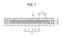
- Fig. 1 is a cross-sectional view showing a relevant part of an embodiment of the FED.
- reference numeral 1 indicates a face plate.
- the face plate 1 has phosphor layers 3 formed on a transparent substrate such as a glass substrate 2.
- the phosphor layers 3 include blue light emitting phosphor layers, green light emitting phosphor layers, and red light emitting phosphor layers formed to correspond pixels, and these layers are isolated from one another with a light absorbing layer 4 composed of a black conductive material filling the gaps between these layers.
- the green light emitting phosphor layers are formed by using the green phosphor of the first embodiment described above.
- the blue light emitting layers and the red light emitting layers are respectively composed of a blue light emitting zinc sulfide phosphor and a red light emitting oxysulfide phosphor known in the art.
- each green light emitting phosphor layer formed of the green phosphor of the first embodiment is preferably 1 to 10 ⁇ m and more preferably 6 to 10 ⁇ m.
- the thickness of the green light emitting phosphor layer is limited to 1 ⁇ m or more since it is difficult to form a phosphor layer less than 1 ⁇ m in thickness with phosphor particles uniformly aligned.
- a green light emitting phosphor layer having a thickness of more than 10 ⁇ m is not suitable for practical application since the luminance is low.
- the thicknesses of the blue and red light emitting phosphor layers are preferably set to be equal to that of the green light emitting phosphor layer.
- the green light emitting phosphor layers, blue light emitting phosphor layers, and red light emitting phosphor layers, and the light absorbing layer 4 that isolates these layers from one anther are arranged in a repeating pattern in the horizontal direction, and the portion where the phosphor layers 3 and the light absorbing layer 4 exist is the image display region.
- Various patterns e.g., a dot pattern or a stripe pattern, are applicable as the pattern of arranging the phosphor layers 3 and the light absorbing layer 4.
- a metal back layer 5 is formed on the phosphor layers 3.
- the metal back layer 5 is a metal film such as an aluminum film and improves the luminance by reflecting light travelling in the rear plate direction described below among light generated in the phosphor layers 3.
- the metal back layer 5 also gives conductivity to the image display region of a face plate 1 to prevent charge from accumulating therein and functions as an anode electrode with respect to the electron source of the rear plate.
- the metal back layer 5 has a function of preventing the phosphor layer 3 from being damaged by ions generated by ionization of gas remaining in the face plate 1, the vacuum container (envelope), etc., by the electron beam.
- the metal back layer 5 also has effects of preventing the gas generated in the phosphor layer 3 during use from being released to the interior of the vacuum container (envelope) and preventing the degree of vacuum from decreasing.
- a getter film 6 composed of an evaporable getter material containing Ba or the like is formed on the metal back layer 5.
- the gas generated during use is efficiently absorbed in the getter film 6.
- the face plate 1 and a rear plate 7 are arranged to face each other with a gap therebetween, and this gap is hermetically sealed by a supporting frame 8.
- the supporting frame 8 is bonded to the face plate 1 and the rear plate 7 with an adhesive 9 composed of a frit glass, In, an In alloy, or the like so as to form a vacuum container, i.e., an envelope, with the face plate 1, the rear plate 7, and the supporting frame 8.
- the rear plate 7 includes a substrate 10 constituted by an insulating substrate such as a glass substrate or a ceramic substrate or a silicon substrate; and many electron emitting elements 11 formed on the substrate 10.
- the electron emitting elements 11 are provided with, for example, field emission cold cathodes or surface-conduction electron-emitting elements and interconnections (not shown in the drawing) are formed on a surface of the rear plate 7 on which the electron emitting elements 11 are formed. That is, many electron emitting elements 11 are arranged in a matrix corresponding to the phosphors of the respective pixels, and interconnections intersecting one another (X-Y interconnections) are provided to drive the electron emitting elements 11, which are arranged in the matrix, row by row.
- X-Y interconnections intersecting one another
- Signal input terminals and row selecting terminals not shown in the drawing are provided to the supporting frame 8. These terminals correspond to the intersecting interconnections (X-Y interconnections) of the rear plate 7 described above.
- X-Y interconnections intersecting interconnections
- an atmospheric pressure supporting member (spacer) 12 may be provided between the face plate 1 and the rear plate 7, if necessary.
- the luminance and color purity of light emitted by irradiation with the pulse electron beam having an accelerating voltage of 5 to 15 kV, more preferably 7 to 12 kV are high, and satisfactory display characteristics can be achieved.
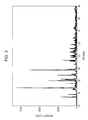
- the resulting fired material was washed with water, dried, and sieved to obtain a europium (Eu)-activated strontium thiogallate phosphor (SrGa 2 S 4 :Eu).
- An XRD (X-ray diffraction) spectrum of the obtained europium-activated strontium thiogallate was measured, and an XRD (X-ray diffraction) pattern shown in Fig. 2 was obtained. No peak was found in the diffraction angle (2 ⁇ ) range of 27° to 29° in the XRD pattern, which confirmed that the europium-activated strontium thiogallate phosphor obtained in Example did not contain gallium sulfide (Ga 2 S 3 ).
- a phosphor layer 10 ⁇ m in thickness was formed by screen printing using the resulting phosphor, and a metal back layer composed of aluminum was formed thereon by a lacquer method.
- a phosphor of Comparative Example was synthesized as in Example 1 except that, during the synthesis, the ratio of Ga to Sr was set slightly in excess of Ga compared to the stoichiometric ratio Ga:Sr of 2:1, i.e., the ratio was set to 2.05: 1.
- the XRD (X-ray diffraction) of the resulting phosphor is shown in Fig. 3 .
- a peak (P) indicative of gallium sulfide (Ga 2 S 3 ) is found in the diffraction angle (2 ⁇ ) range of 27° to 29° in the XRD pattern.
- a green phosphor layer was formed in the same manner by using a phosphor containing gallium sulfide (Ga 2 S 3 ), and a metal back layer composed of aluminum was formed thereon by a lacquer method.
- the luminance and luminescent chromaticity of the phosphor layers of Example 1 and Comparative Example were studied.
- the luminance was measured by irradiating each phosphor layer with an electron beam having an accelerating voltage of 10 kV and a current density of 40 mA/cm 2 .
- the luminance was determined as a relative value by assuming the luminance of the phosphor layer of Comparative Example to be 100.
- the luminescent chromaticity was measured with SR-3 by Topcon Corporation. Measurement of the luminescent chromaticity was conducted in a darkroom in which the chromaticity during emission was unaffected by outside factors. The measurement results of the luminance and the luminescent chromaticity are shown in Table 1.
- Table 1 Phosphor composition Luminance (%) Luminescent chromaticity (x, y)
- the europium (Eu)-activated strontium thiogallate phosphor obtained in Example 1 exhibits a significantly improved luminance when irradiated with a pulse electron beam having a low accelerating voltage (5 to 15 kV) and a high current density.
- the table also shows that the phosphor also has a sufficiently high luminescent chromaticity.
- the face plate was assembled with a rear plate having many electron emitting elements with a supporting frame, and the gap between the plates was hermetically sealed under vacuuming. It was confirmed that the FED thus produced exhibited excellent color reproducibility including luminance and that satisfactory luminance characteristic was exhibited after 1000 hours of driving under rated operation.
- green light having a high luminance and a satisfactory color purity can be emitted by irradiation with a pulse electron beam having an accelerating voltage of 5 to 15 kV and a high current density.
- a flat, thin display having excellent display characteristics such as high luminance and color reproducibility can be realized by using this green phosphor.
Abstract
Description
- The present invention relates to a phosphor for displays and a field emission display incorporating the phosphor.
- With advent of the multimedia age, for displays which are core devices of digital networks, achievement of increased screen size, higher definition, and compatibility with various sources such as computers is required.
- Among displays, field emission displays (FEDs) that use field emission elements such as field emission cold cathodes are currently being increasingly and extensively studied and developed as large-screen thin digital devices that can display various types of information at high density and with high definition.
- The basic display principle of the FEDs is the same as that of cathode ray tubes (CRTs), i.e., a phosphor is excited by electron beams so that the phosphor emits light. However, the accelerating voltage (excitation voltage) of the electron beam is lower than that of CRTs, and the current density per unit time obtainable by the electron beam is also low. Thus, in order to achieve a sufficient luminance, a significantly long excitation time is required compared to CRTs. This means that the quantity of charges injected per unit area needs to be increased to achieve a particular luminance, and this shortens the lifetime of the phosphor. Consequently, sufficient luminance and lifetime have not been obtained with zinc sulfide-based phosphors that have been used in CRTs in the related art. Under these circumstances, a phosphor for FEDs that has high luminance is desired (e.g., refer to Patent Document 1).
- An europium-activated thiogallate phosphor represented by a chemical formula, SrGa2S4:Eu has been known to exhibit a relatively good emission intensity particularly when irradiated with an electron beam having an excitation voltage of 5 kV or less. Since this phosphor has a good luminescent color, it is known as a phosphor that can be used in general CRTs although the luminance thereof is not as good as that of the zinc sulfide phosphor.
- However, in FEDs having an excitation voltage of 5 to 15 kV, it is not likely that this phosphor can be directly used. In order to improve the emission characteristics of the FEDs, development of a phosphor for FEDs that has excellent emission characteristics is desired. Patent Document 1: Japanese Patent Laid-Open No.
2002-226847 - The present invention is made to overcome the above-described problems and aims to provide a phosphor for a displays having a high luminance. It is also an object of the present invention to provide a field emission display (FED) having a high luminance and excellent display characteristics such as color reproducibility by using such a phosphor.
- A phosphor for a display of the present invention includes a europium (Eu)-activated thiogallate phosphor substantially represented by a chemical formula, SrGa2S4:Eu free of gallium sulfide represented by a chemical formula, Ga2S3, in which the phosphor is a green phosphor that emits light when excited by an electron beam having an accelerating voltage of 5 to 15 kV.
- A field emission display of the present invention includes phosphor layers including blue light emitting phosphor layers, green light emitting phosphor layers, and red light emitting phosphor layers; an electron source configured to irradiate the phosphor layers with an electron beam having an accelerating voltage of 5 to 15 kV; and an envelope configured to vacuum seal the electron source and the phosphor layers, in which the green light emitting phosphor layers include the phosphor for the display of the present invention described above.
- Since the phosphor for the display of the present invention contains, as a matrix, strontium thiogallate (SrGa2S4), i.e., a ternary compound of strontium (Sr), gallium (Ga), and sulfur (S), and, as an activator, europium (Eu) whose electronic state makes transition from the ground level to an excited level at a high probability, excellent luminous efficiency is achieved by irradiation with a pulse electron beam having an accelerating voltage of 5 to 15 kV, and high luminance is obtained.
- Compared to zinc sulfide phosphors and oxysulfide phosphors that have been used as the phosphors for CRTs in the related art, long lifetime is achieved. Thus, when the phosphor for the display is used, a thin, flat display, such as a FED, having a high luminance, excellent display characteristics, and a long lifetime can be realized. Brief Description of Drawings
- [
Fig. 1 ] A cross-sectional view schematically showing a FED according to a second embodiment of the present invention. - [
Fig. 2 ] A graph showing an XRD (X-ray diffraction) pattern of a europium-activated strontium thiogallate phosphor obtained in Example 1 of the present invention. - [
Fig. 3 ] A graph showing an XRD (X-ray diffraction) pattern of a phosphor obtained in Comparative Example of the present invention. - Preferred embodiments of the present invention will now be described. The present invention is not limited to the embodiments described below.
- A first embodiment of the present invention is a phosphor composed of a ternary compound containing strontium (Sr) of Group II, gallium (Ga) of Group III, and sulfur (S) of Group VI in the periodic table with europium (Eu) serving as an activator. The phosphor is substantially free of gallium sulfide represented by Ga2S3. To be more specific, the phosphor is a europium-activated strontium thiogallate phosphor represented by chemical formula SrGa2S4:Eu and emits green light when excited by a pulse electron beam having an accelerating voltage of 5 to 15 kV and preferably 7 to 12 kV.
- In this phosphor, europium is an activator that forms the luminescent center and exhibits a high luminous efficiency due to its high transition probability. Europium serving as the activator is preferably contained in an amount of 0.1 to 5.0 mol% relative to strontium thiogallate (SrGa2S4), which is the matrix of the phosphor. A more preferred Eu content range is 1.5 to 4.0 mol%. It is not preferable that the Eu content be outside this range since the luminance and luminescent chromaticity would be degraded.
- The europium-activated strontium thiogallate phosphor of the first embodiment can be made by the following process, for example.
- That is, phosphor starting materials containing elements constituting the matrix and the activator of the phosphor or compounds containing such elements are weighed so that a desired composition (SrGa2S4:Eu) is achieved, and then dry-mixed. To be more specific, appropriate amounts of strontium sulfide and gallium oxyhydroxide are mixed, and an appropriate amount of activator (or a compound containing activator) is added to the resulting mixture to prepare the material of the phosphor. Instead of strontium sulfide, an acidic strontium material such as strontium sulfate may be used. As the activator, europium sulfide or europium oxalate may be used.
- Here, the mixture ratio of Sr to Ga as elements is set to 1:2, which is a stoichiometric ratio. According to past reports, addition of excess Ga is required to achieve sufficient reaction; however, if Ga is added in excess, gallium sulfide represented by Ga2S3 will be produced as a byproduct and remain in the SrGa2S4 phosphor. This is not preferable.
- A heat-resistant container such as an alumina crucible or a quartz crucible is then filled with the phosphor material and adequate amounts of sulfur and activated carbon. In adding and mixing sulfur, it is preferable to mix an amount of sulfur slightly larger than that of the phosphor by using a blender or the like so that after the mixed material is filled into the heat resistant container, the surface thereof is covered with sulfur. The material is then fired in a sulfurizing atmosphere such as a hydrogen sulfide atmosphere or a sulfur vapor atmosphere or a reducing atmosphere (e.g., a 3-5% hydrogen/balance nitrogen atmosphere).
- The firing conditions are important for controlling the crystal structure of the phosphor matrix (SrGa2S4). The firing temperature is preferably in the range of 700°C to 900°C. The time of firing depends on the firing temperature set but is 60 to 180 minutes. After firing, cooling is preferably conducted in the same atmosphere as firing. Subsequently, after the fired material is washed with water such as ion exchanged water and dried, a process such as sieving is conducted, if necessary, to remove coarse particles so as to obtain an europium-activated strontium thiogallate phosphor (SrGa2S4:Eu).
- The europium-activated strontium thiogallate phosphor of the first embodiment can also be synthesized from starting materials such as metallic gallium and strontium sulfide or strontium sulfate. Firing may be conducted under the above-described firing conditions (temperature and time).
- It is also possible to fire the phosphor material in a rotary heating furnace as follows. That is, the phosphor material is loaded into a tubular rotary furnace disposed obliquely with respect to the horizontal direction and rotated about the center axis so that the phosphor material passes through the furnace continuously. The phosphor material is then rapidly heated to a predetermined firing temperature in the heating furnace while the being tumbled in the rotating heating furnace so that the phosphor material moves from the upper part to the lower part of the furnace. With this operation, the phosphor material is fired by being heated for a sufficient and necessary time. Subsequently, the fired phosphor material is continuously discharged from the heating furnace and rapidly cooled.
- In such a firing process, the interior of the tubular heating furnace and the cooling unit for the fired material discharged from the heating furnace are preferably retained in a state with oxygen removed therefrom (oxygen-free state). In particular, the interior of the heating furnace is preferably retained in a hydrogen sulfide atmosphere.
- According to this firing process, the phosphor material moving inside the heating furnace is rapidly heated while being tumbled, and heat energy is uniformly applied to the phosphor material in an oxygen-free hydrogen sulfide atmosphere or the like. Thus, firing can be completed in a shorter time than when a crucible is used for firing. Consequently, a phosphor with smaller particle diameter can be obtained without degrading the luminance. Moreover, since aggregation of the phosphor particles can be suppressed, there is no need to conduct further pulverization after firing. Thus, deterioration of the phosphor resulting from the pulverization step can be suppressed. Since the phosphor material is heated and fired while being tumbled in the heating furnace, phosphor particles substantially spherical in shape and uniform in particle diameter can be obtained.
- According to the firing method that uses the rotary heating furnace or the crucible, a europium-activated strontium thiogallate (SrGa2S4:Eu) phosphor substantially free of gallium sulfide (Ga2S3) can be obtained. That this SrGa2S4:Eu phosphor is substantially free of Ga2S3 can be confirmed by analyzing an XRD (X-ray diffraction) pattern. In other words, if gallium sulfide (Ga2S3) is contained in the phosphor, a peak indicating the existence of Ga2S3 will appear in the diffraction angle (2θ) range of 27° to 29° in the XRD pattern. Absence of this peak would confirm that the phosphor is substantially free of Ga2S3.
- The europium (Eu)-activated strontium thiogallate phosphor of the first embodiment thus obtained is a phosphor that emits green light when irradiated with a pulse electron beam at an accelerating voltage of 5 to 15 kV and preferably 7 to 12 kV and has a good luminous efficiency, thereby achieving a high luminance. A high-luminance FED can be realized by using this phosphor.
- A green phosphor layer can be formed by using the green phosphor of the first embodiment and an existing printing or slurry method. In order to form a phosphor layer by a printing method, the phosphor of the first embodiment is mixed with a binder solution containing, e.g., polyvinyl alcohol, n-butyl alcohol, ethylene glycol, and water, to prepare a phosphor paste, and the phosphor paste is applied onto a substrate by a method such as screen-printing or the like. A baking process is then conducted in which the applied paste is heated at 500°C for 1 hour to decompose and remove the binder components.
- In a slurry method, the green phosphor of the first embodiment is mixed with pure water, polyvinyl alcohol, a photosensitive material such as ammonium dichromate, a surfactant, and the like to prepare a phosphor slurry, and the phosphor slurry is then applied onto a substrate with a spin coater or the like and dried. The dried phosphor slurry is irradiated with ultraviolet light or the like to conduct exposure and development, and dried. As a result, a green phosphor layer having an appropriate pattern is formed.
- Next, a field emission display (FED) in which a green light emitting phosphor layer is formed by using the green phosphor of the first embodiment is described.
-
Fig. 1 is a cross-sectional view showing a relevant part of an embodiment of the FED. InFig. 1 ,reference numeral 1 indicates a face plate. Theface plate 1 hasphosphor layers 3 formed on a transparent substrate such as aglass substrate 2. The phosphor layers 3 include blue light emitting phosphor layers, green light emitting phosphor layers, and red light emitting phosphor layers formed to correspond pixels, and these layers are isolated from one another with a lightabsorbing layer 4 composed of a black conductive material filling the gaps between these layers. The green light emitting phosphor layers are formed by using the green phosphor of the first embodiment described above. The blue light emitting layers and the red light emitting layers are respectively composed of a blue light emitting zinc sulfide phosphor and a red light emitting oxysulfide phosphor known in the art. - The thickness of each green light emitting phosphor layer formed of the green phosphor of the first embodiment is preferably 1 to 10 µm and more preferably 6 to 10 µm. The thickness of the green light emitting phosphor layer is limited to 1 µm or more since it is difficult to form a phosphor layer less than 1 µm in thickness with phosphor particles uniformly aligned. A green light emitting phosphor layer having a thickness of more than 10 µm is not suitable for practical application since the luminance is low. In order to eliminate differences in height among the phosphor layers 3 of respective colors, the thicknesses of the blue and red light emitting phosphor layers are preferably set to be equal to that of the green light emitting phosphor layer.
- The green light emitting phosphor layers, blue light emitting phosphor layers, and red light emitting phosphor layers, and the
light absorbing layer 4 that isolates these layers from one anther are arranged in a repeating pattern in the horizontal direction, and the portion where the phosphor layers 3 and thelight absorbing layer 4 exist is the image display region. Various patterns, e.g., a dot pattern or a stripe pattern, are applicable as the pattern of arranging the phosphor layers 3 and thelight absorbing layer 4. - A metal back
layer 5 is formed on the phosphor layers 3. The metal backlayer 5 is a metal film such as an aluminum film and improves the luminance by reflecting light travelling in the rear plate direction described below among light generated in the phosphor layers 3. The metal backlayer 5 also gives conductivity to the image display region of aface plate 1 to prevent charge from accumulating therein and functions as an anode electrode with respect to the electron source of the rear plate. The metal backlayer 5 has a function of preventing thephosphor layer 3 from being damaged by ions generated by ionization of gas remaining in theface plate 1, the vacuum container (envelope), etc., by the electron beam. The metal backlayer 5 also has effects of preventing the gas generated in thephosphor layer 3 during use from being released to the interior of the vacuum container (envelope) and preventing the degree of vacuum from decreasing. - A
getter film 6 composed of an evaporable getter material containing Ba or the like is formed on the metal backlayer 5. The gas generated during use is efficiently absorbed in thegetter film 6. Theface plate 1 and arear plate 7 are arranged to face each other with a gap therebetween, and this gap is hermetically sealed by a supporting frame 8. The supporting frame 8 is bonded to theface plate 1 and therear plate 7 with an adhesive 9 composed of a frit glass, In, an In alloy, or the like so as to form a vacuum container, i.e., an envelope, with theface plate 1, therear plate 7, and the supporting frame 8. - The
rear plate 7 includes asubstrate 10 constituted by an insulating substrate such as a glass substrate or a ceramic substrate or a silicon substrate; and manyelectron emitting elements 11 formed on thesubstrate 10. Theelectron emitting elements 11 are provided with, for example, field emission cold cathodes or surface-conduction electron-emitting elements and interconnections (not shown in the drawing) are formed on a surface of therear plate 7 on which theelectron emitting elements 11 are formed. That is, manyelectron emitting elements 11 are arranged in a matrix corresponding to the phosphors of the respective pixels, and interconnections intersecting one another (X-Y interconnections) are provided to drive theelectron emitting elements 11, which are arranged in the matrix, row by row. Signal input terminals and row selecting terminals not shown in the drawing are provided to the supporting frame 8. These terminals correspond to the intersecting interconnections (X-Y interconnections) of therear plate 7 described above. In increasing the size of a flat FED, there is a risk of bowing because of its flat, thin shape. In order to prevent bowing and impart strength relative to the atmospheric pressure, an atmospheric pressure supporting member (spacer) 12 may be provided between theface plate 1 and therear plate 7, if necessary. - According to the FED of the second embodiment having green light emitting phosphor layers formed of the green phosphor of the first embodiment, the luminance and color purity of light emitted by irradiation with the pulse electron beam having an accelerating voltage of 5 to 15 kV, more preferably 7 to 12 kV are high, and satisfactory display characteristics can be achieved.
- Specific examples of the present invention will now be described.
- Starting materials containing elements constituting the matrix of the phosphor and the activator or compounds containing such elements were weighed so that the stoichiometric ratio of the composition shown in Table 1 (SrGa2S4:Eu, Eu content being 2 mol%) was achieved, and thoroughly mixed. The resulting phosphor material was filled in a quartz crucible with adequate amounts of sulfur and activated carbon, and fired in a hydrogen sulfide atmosphere. The firing condition was 800°C × 60 min.
- The resulting fired material was washed with water, dried, and sieved to obtain a europium (Eu)-activated strontium thiogallate phosphor (SrGa2S4:Eu). An XRD (X-ray diffraction) spectrum of the obtained europium-activated strontium thiogallate was measured, and an XRD (X-ray diffraction) pattern shown in
Fig. 2 was obtained. No peak was found in the diffraction angle (2θ) range of 27° to 29° in the XRD pattern, which confirmed that the europium-activated strontium thiogallate phosphor obtained in Example did not contain gallium sulfide (Ga2S3). - Next, a
phosphor layer 10 µm in thickness was formed by screen printing using the resulting phosphor, and a metal back layer composed of aluminum was formed thereon by a lacquer method. - A phosphor of Comparative Example was synthesized as in Example 1 except that, during the synthesis, the ratio of Ga to Sr was set slightly in excess of Ga compared to the stoichiometric ratio Ga:Sr of 2:1, i.e., the ratio was set to 2.05: 1. The XRD (X-ray diffraction) of the resulting phosphor is shown in
Fig. 3 . As is apparent from the pattern, a peak (P) indicative of gallium sulfide (Ga2S3) is found in the diffraction angle (2θ) range of 27° to 29° in the XRD pattern. Next, a green phosphor layer was formed in the same manner by using a phosphor containing gallium sulfide (Ga2S3), and a metal back layer composed of aluminum was formed thereon by a lacquer method. - The luminance and luminescent chromaticity of the phosphor layers of Example 1 and Comparative Example were studied. The luminance was measured by irradiating each phosphor layer with an electron beam having an accelerating voltage of 10 kV and a current density of 40 mA/cm2. The luminance was determined as a relative value by assuming the luminance of the phosphor layer of Comparative Example to be 100.
- The luminescent chromaticity was measured with SR-3 by Topcon Corporation. Measurement of the luminescent chromaticity was conducted in a darkroom in which the chromaticity during emission was unaffected by outside factors. The measurement results of the luminance and the luminescent chromaticity are shown in Table 1.
Table 1 Phosphor composition Luminance (%) Luminescent chromaticity (x, y) Example 1 SrGa2S4:Eu 115 0.270, 0.678 Comparative Example SrGa2S4:Eu (with Ga2S3) 100 0.276, 0.679 - As is apparent from Table 1, compared to the phosphor of Comparative Example containing a trace amount of gallium sulfide (Ga2S3), the europium (Eu)-activated strontium thiogallate phosphor obtained in Example 1 exhibits a significantly improved luminance when irradiated with a pulse electron beam having a low accelerating voltage (5 to 15 kV) and a high current density. Moreover, the table also shows that the phosphor also has a sufficiently high luminescent chromaticity.
- The europium (Eu)-activated strontium thiogallate phosphor (SrGa2S4:Eu) obtained in Example 1, a known blue light emitting phosphor (ZnS:Ag,Al), and a known red light emitting phosphor (Y2O2S:Eu) were used to form phosphor layers on a glass substrate to thereby form a face plate. The face plate was assembled with a rear plate having many electron emitting elements with a supporting frame, and the gap between the plates was hermetically sealed under vacuuming. It was confirmed that the FED thus produced exhibited excellent color reproducibility including luminance and that satisfactory luminance characteristic was exhibited after 1000 hours of driving under rated operation.
- According to the phosphor for a display of the present invention, green light having a high luminance and a satisfactory color purity can be emitted by irradiation with a pulse electron beam having an accelerating voltage of 5 to 15 kV and a high current density. Thus, a flat, thin display having excellent display characteristics such as high luminance and color reproducibility can be realized by using this green phosphor.
Claims (3)
- A phosphor for a display, comprising a europium (Eu)-activated thiogallate phosphor substantially represented by a chemical formula, SrGa2S4:Eu free of gallium sulfide represented by a chemical formula, Ga2S3, wherein the phosphor is a green phosphor that emits light when excited by an electron beam having an accelerating voltage of 5 to 15 kV.
- The phosphor for the display according to claim 1, wherein an XRD (X-ray diffraction) pattern of the europium-activated thiogallate phosphor has no peak indicative of gallium sulfide (Ga2S3) in a diffraction angle (2θ) range of 27° to 29°.
- A field emission display comprising phosphor layers including blue light emitting phosphor layers, green light emitting phosphor layers, and red light emitting phosphor layers; an electron source configured to irradiate the phosphor layers with an electron beam having an accelerating voltage of 5 to 15 kV; and an envelope configured to vacuum seal the electron source and the phosphor layers,
wherein the green light emitting phosphor layers include the phosphor for the display according to claim 1 or 2.
Applications Claiming Priority (2)
| Application Number | Priority Date | Filing Date | Title |
|---|---|---|---|
| JP2006065058A JP2007238827A (en) | 2006-03-10 | 2006-03-10 | Phosphor for display device and field emission type display device |
| PCT/JP2007/000188 WO2007105370A1 (en) | 2006-03-10 | 2007-03-09 | Phosphor for display and field emission display |
Publications (2)
| Publication Number | Publication Date |
|---|---|
| EP1995295A1 true EP1995295A1 (en) | 2008-11-26 |
| EP1995295A4 EP1995295A4 (en) | 2010-08-04 |
Family
ID=38509211
Family Applications (1)
| Application Number | Title | Priority Date | Filing Date |
|---|---|---|---|
| EP07713570A Withdrawn EP1995295A4 (en) | 2006-03-10 | 2007-03-09 | Phosphor for display and field emission display |
Country Status (6)
| Country | Link |
|---|---|
| US (1) | US20090039759A1 (en) |
| EP (1) | EP1995295A4 (en) |
| JP (1) | JP2007238827A (en) |
| CN (1) | CN101389732A (en) |
| TW (1) | TW200739650A (en) |
| WO (1) | WO2007105370A1 (en) |
Families Citing this family (10)
| Publication number | Priority date | Publication date | Assignee | Title |
|---|---|---|---|---|
| JP2007321139A (en) * | 2006-06-05 | 2007-12-13 | National Univ Corp Shizuoka Univ | Method for producing fluorophor, the resultant fluorophor, light-emitting device, light emitter, image display, and illuminator |
| CN101441972B (en) | 2007-11-23 | 2011-01-26 | 鸿富锦精密工业(深圳)有限公司 | Field emission pixel tube |
| CN101452797B (en) | 2007-12-05 | 2011-11-09 | 清华大学 | Field emission type electronic source and manufacturing method thereof |
| JP5503105B2 (en) * | 2007-12-26 | 2014-05-28 | 日本放送協会 | Cathode ray tube for viewfinder |
| US8147717B2 (en) | 2008-09-11 | 2012-04-03 | Mitsui Mining & Smelting Co., Ltd. | Green emitting phosphor |
| JP2010123499A (en) * | 2008-11-21 | 2010-06-03 | Canon Inc | Manufacturing method of phosphor substrate and image display device |
| CN102471684B (en) * | 2009-09-18 | 2014-10-01 | 三井金属矿业株式会社 | Phosphor |
| US20120211783A1 (en) * | 2010-11-17 | 2012-08-23 | Ncku Research And Development Foundation | Light-emitting-diode array with microstructures in gap between light-emitting-diodes |
| CN104059637B (en) * | 2013-03-20 | 2016-01-13 | 海洋王照明科技股份有限公司 | Metal nano particle-doped strontium thiogallate luminescent material and preparation method |
| CN104059636B (en) * | 2013-03-20 | 2016-04-27 | 海洋王照明科技股份有限公司 | Metal nano particle-doped ternary sulfide luminescent material and preparation method |
Citations (1)
| Publication number | Priority date | Publication date | Assignee | Title |
|---|---|---|---|---|
| US20020190241A1 (en) * | 2001-06-13 | 2002-12-19 | Thierry Le Mercier | Compound based on an alkaline-earth metal, sulphur and aluminium, gallium or indium, its method of preparation and its use as a phosphor |
Family Cites Families (15)
| Publication number | Priority date | Publication date | Assignee | Title |
|---|---|---|---|---|
| US4116864A (en) * | 1975-05-12 | 1978-09-26 | Dai Nippon Toryo Co. Ltd. | Fluorescent compositions for low-velocity electron excited fluorescent display devices |
| US4208613A (en) * | 1975-06-30 | 1980-06-17 | Dai Nippon Toryo Co., Ltd. | Low-velocity electron excited fluorescent display device |
| FR2755122B1 (en) * | 1996-10-31 | 1998-11-27 | Rhodia Chimie Sa | COMPOUND BASED ON AN ALKALINE EARTH, SULFUR AND ALUMINUM, GALLIUM OR INDIUM, METHOD FOR PREPARING SAME AND USE THEREOF AS LUMINOPHORE |
| US6875372B1 (en) * | 1997-02-24 | 2005-04-05 | Cabot Corporation | Cathodoluminescent phosphor powders, methods for making phosphor powders and devices incorporating same |
| CA2348641A1 (en) * | 1998-08-31 | 2001-04-19 | The Government Of The United States Of America As Represented By The Secretary Of The Navy | Coated cathodoluminescent phosphors |
| JP2000221623A (en) * | 1999-01-28 | 2000-08-11 | Fuji Photo Film Co Ltd | Planar image intensifier and radiation image forming method |
| JP2001185050A (en) * | 1999-12-27 | 2001-07-06 | Kasei Optonix Co Ltd | Method of manufacturing fluorescent film |
| JP2002226847A (en) | 2000-04-11 | 2002-08-14 | Toshiba Corp | Fluorescent substance for display device and field emission type display device using thereof |
| TW567222B (en) * | 2000-04-11 | 2003-12-21 | Toshiba Corp | Phosphor for display and field-emission display |
| US6544438B2 (en) * | 2000-08-02 | 2003-04-08 | Sarnoff Corporation | Preparation of high emission efficiency alkaline earth metal thiogallate phosphors |
| USH2219H1 (en) * | 2000-10-31 | 2008-07-01 | The United States Of America As Represented By The Secretary Of The Navy | Method for coating small particles |
| KR101209488B1 (en) * | 2004-07-06 | 2012-12-07 | 라이트스케이프 머티어리얼스, 인코포레이티드 | Efficient, green-emitting phosphors, and combinations with red-emitting phosphors |
| US7390437B2 (en) * | 2004-08-04 | 2008-06-24 | Intematix Corporation | Aluminate-based blue phosphors |
| JP4543253B2 (en) * | 2004-10-28 | 2010-09-15 | Dowaエレクトロニクス株式会社 | Phosphor mixture and light emitting device |
| WO2007143379A2 (en) * | 2006-05-30 | 2007-12-13 | University Of Georgia Research Foundation | White phosphors, methods of making white phosphors, white light emitting leds, methods of making white light emitting leds, and light bulb structures |
-
2006
- 2006-03-10 JP JP2006065058A patent/JP2007238827A/en not_active Withdrawn
-
2007
- 2007-03-09 CN CNA2007800062627A patent/CN101389732A/en active Pending
- 2007-03-09 EP EP07713570A patent/EP1995295A4/en not_active Withdrawn
- 2007-03-09 TW TW096108286A patent/TW200739650A/en not_active IP Right Cessation
- 2007-03-09 US US12/280,945 patent/US20090039759A1/en not_active Abandoned
- 2007-03-09 WO PCT/JP2007/000188 patent/WO2007105370A1/en active Application Filing
Patent Citations (1)
| Publication number | Priority date | Publication date | Assignee | Title |
|---|---|---|---|---|
| US20020190241A1 (en) * | 2001-06-13 | 2002-12-19 | Thierry Le Mercier | Compound based on an alkaline-earth metal, sulphur and aluminium, gallium or indium, its method of preparation and its use as a phosphor |
Non-Patent Citations (3)
| Title |
|---|
| NAKAJIMA H ET AL: "Preparation of SrGa2S4:Ce thin films for low-energy cathodoluminescence" JOURNAL OF LUMINESCENCE MAY 2000 ELSEVIER SCIENCE PUBLISHERS B.V., vol. 87, 23 August 1999 (1999-08-23), pages 1146-1148, XP002587202 DOI: DOI:10.1016/S0022-2313(99)00572-4 * |
| See also references of WO2007105370A1 * |
| TANAKA K ET AL: "Blue luminescent SrGa2S4: Ce thin films grown by molecular beam epitaxy" JOURNAL OF CRYSTAL GROWTH, ELSEVIER, AMSTERDAM, NL LNKD- DOI:10.1016/0022-0248(95)80131-U, vol. 150, no. 9714, 1 May 1995 (1995-05-01), pages 1211-1214, XP004003684 ISSN: 0022-0248 * |
Also Published As
| Publication number | Publication date |
|---|---|
| CN101389732A (en) | 2009-03-18 |
| EP1995295A4 (en) | 2010-08-04 |
| TW200739650A (en) | 2007-10-16 |
| WO2007105370A1 (en) | 2007-09-20 |
| TWI341545B (en) | 2011-05-01 |
| JP2007238827A (en) | 2007-09-20 |
| US20090039759A1 (en) | 2009-02-12 |
Similar Documents
| Publication | Publication Date | Title |
|---|---|---|
| EP1995295A1 (en) | Phosphor for display and field emission display | |
| US4791336A (en) | Fluorescent composition and fluorescent luminous device | |
| JP4931175B2 (en) | Phosphor for electron beam excited light emitting device, method for producing the same, and electron beam excited light emitting device | |
| KR100821047B1 (en) | Blue phosphor and display panel using the same | |
| JP4931176B2 (en) | Phosphor, method for manufacturing the same, and light emitting device | |
| WO2006129593A1 (en) | Phosphor for display and field emission display | |
| EP1772508A1 (en) | Display unit-use blue light emitting fluorescent substance and production method therefor and field emission type display unit | |
| KR100676352B1 (en) | Fluorescent material for display unit, process for producing the same and color display unit including the same | |
| JP4873910B2 (en) | Phosphor for electron beam excited light emitting device, method for producing the same, and electron beam excited light emitting device | |
| WO2006120952A1 (en) | Blue light emitting phosphor for display unit and field emission display unit | |
| JP4873909B2 (en) | Phosphor for electron beam excited light emitting device, method for producing the same, and electron beam excited light emitting device | |
| EP1607461A1 (en) | Green light emitting phosphor for low voltage/high current density and field emissiion type display including the same | |
| US20080265743A1 (en) | Green Light-Emitting Phosphor for Displays and Field-Emission Display Using Same | |
| JP2008140617A (en) | Red light-emitting element and field emission display device | |
| JP2007329027A (en) | Field emission display | |
| JP2007177078A (en) | Fluorophor for display device and field emission-type display device | |
| JP2008127465A (en) | Method for producing phosphor, device for producing the same and electric field emission type displaying device | |
| JP2008184528A (en) | Phosphor for displaying device and field emission type displaying device | |
| JP2008130305A (en) | Green light-emitting element, and field emission display device | |
| JP2006316105A (en) | Green color-emitting fluorophor for display device and field emission-type display device | |
| JP2008156581A (en) | Phosphor for display apparatus and field emission display | |
| JP2005036111A (en) | Phosphor for display device and method for producing the same, and field emission display device using the same | |
| JP2008179748A (en) | Red light emitting device and field emission type display device | |
| JP2005089496A (en) | Phosphor composition, method for producing the same and fluorescent display apparatus and method for emitting light using the same | |
| JP2004123787A (en) | Phosphor for display device and color display device using the same |
Legal Events
| Date | Code | Title | Description |
|---|---|---|---|
| PUAI | Public reference made under article 153(3) epc to a published international application that has entered the european phase |
Free format text: ORIGINAL CODE: 0009012 |
|
| 17P | Request for examination filed |
Effective date: 20081010 |
|
| AK | Designated contracting states |
Kind code of ref document: A1 Designated state(s): DE FR GB |
|
| RBV | Designated contracting states (corrected) |
Designated state(s): DE FR GB |
|
| RBV | Designated contracting states (corrected) |
Designated state(s): AT BE BG CH CY CZ DE DK EE ES FI FR GB GR HU IE IS IT LI LT LU LV MC MT NL PL PT RO SE SI SK TR |
|
| A4 | Supplementary search report drawn up and despatched |
Effective date: 20100705 |
|
| STAA | Information on the status of an ep patent application or granted ep patent |
Free format text: STATUS: THE APPLICATION HAS BEEN WITHDRAWN |
|
| 18W | Application withdrawn |
Effective date: 20120201 |