EP1988190A2 - Coated cutting tool - Google Patents
Coated cutting tool Download PDFInfo
- Publication number
- EP1988190A2 EP1988190A2 EP08103610A EP08103610A EP1988190A2 EP 1988190 A2 EP1988190 A2 EP 1988190A2 EP 08103610 A EP08103610 A EP 08103610A EP 08103610 A EP08103610 A EP 08103610A EP 1988190 A2 EP1988190 A2 EP 1988190A2
- Authority
- EP
- European Patent Office
- Prior art keywords
- cutting tool
- pvd
- layer
- gpa
- tool according
- Prior art date
- Legal status (The legal status is an assumption and is not a legal conclusion. Google has not performed a legal analysis and makes no representation as to the accuracy of the status listed.)
- Withdrawn
Links
Images
Classifications
-
- C—CHEMISTRY; METALLURGY
- C23—COATING METALLIC MATERIAL; COATING MATERIAL WITH METALLIC MATERIAL; CHEMICAL SURFACE TREATMENT; DIFFUSION TREATMENT OF METALLIC MATERIAL; COATING BY VACUUM EVAPORATION, BY SPUTTERING, BY ION IMPLANTATION OR BY CHEMICAL VAPOUR DEPOSITION, IN GENERAL; INHIBITING CORROSION OF METALLIC MATERIAL OR INCRUSTATION IN GENERAL
- C23C—COATING METALLIC MATERIAL; COATING MATERIAL WITH METALLIC MATERIAL; SURFACE TREATMENT OF METALLIC MATERIAL BY DIFFUSION INTO THE SURFACE, BY CHEMICAL CONVERSION OR SUBSTITUTION; COATING BY VACUUM EVAPORATION, BY SPUTTERING, BY ION IMPLANTATION OR BY CHEMICAL VAPOUR DEPOSITION, IN GENERAL
- C23C14/00—Coating by vacuum evaporation, by sputtering or by ion implantation of the coating forming material
- C23C14/0021—Reactive sputtering or evaporation
- C23C14/0036—Reactive sputtering
- C23C14/0057—Reactive sputtering using reactive gases other than O2, H2O, N2, NH3 or CH4
-
- B—PERFORMING OPERATIONS; TRANSPORTING
- B22—CASTING; POWDER METALLURGY
- B22F—WORKING METALLIC POWDER; MANUFACTURE OF ARTICLES FROM METALLIC POWDER; MAKING METALLIC POWDER; APPARATUS OR DEVICES SPECIALLY ADAPTED FOR METALLIC POWDER
- B22F5/00—Manufacture of workpieces or articles from metallic powder characterised by the special shape of the product
-
- B—PERFORMING OPERATIONS; TRANSPORTING
- B22—CASTING; POWDER METALLURGY
- B22F—WORKING METALLIC POWDER; MANUFACTURE OF ARTICLES FROM METALLIC POWDER; MAKING METALLIC POWDER; APPARATUS OR DEVICES SPECIALLY ADAPTED FOR METALLIC POWDER
- B22F10/00—Additive manufacturing of workpieces or articles from metallic powder
- B22F10/10—Formation of a green body
- B22F10/16—Formation of a green body by embedding the binder within the powder bed
-
- B—PERFORMING OPERATIONS; TRANSPORTING
- B22—CASTING; POWDER METALLURGY
- B22F—WORKING METALLIC POWDER; MANUFACTURE OF ARTICLES FROM METALLIC POWDER; MAKING METALLIC POWDER; APPARATUS OR DEVICES SPECIALLY ADAPTED FOR METALLIC POWDER
- B22F3/00—Manufacture of workpieces or articles from metallic powder characterised by the manner of compacting or sintering; Apparatus specially adapted therefor ; Presses and furnaces
-
- B—PERFORMING OPERATIONS; TRANSPORTING
- B33—ADDITIVE MANUFACTURING TECHNOLOGY
- B33Y—ADDITIVE MANUFACTURING, i.e. MANUFACTURING OF THREE-DIMENSIONAL [3D] OBJECTS BY ADDITIVE DEPOSITION, ADDITIVE AGGLOMERATION OR ADDITIVE LAYERING, e.g. BY 3D PRINTING, STEREOLITHOGRAPHY OR SELECTIVE LASER SINTERING
- B33Y10/00—Processes of additive manufacturing
-
- B—PERFORMING OPERATIONS; TRANSPORTING
- B33—ADDITIVE MANUFACTURING TECHNOLOGY
- B33Y—ADDITIVE MANUFACTURING, i.e. MANUFACTURING OF THREE-DIMENSIONAL [3D] OBJECTS BY ADDITIVE DEPOSITION, ADDITIVE AGGLOMERATION OR ADDITIVE LAYERING, e.g. BY 3D PRINTING, STEREOLITHOGRAPHY OR SELECTIVE LASER SINTERING
- B33Y70/00—Materials specially adapted for additive manufacturing
- B33Y70/10—Composites of different types of material, e.g. mixtures of ceramics and polymers or mixtures of metals and biomaterials
-
- C—CHEMISTRY; METALLURGY
- C04—CEMENTS; CONCRETE; ARTIFICIAL STONE; CERAMICS; REFRACTORIES
- C04B—LIME, MAGNESIA; SLAG; CEMENTS; COMPOSITIONS THEREOF, e.g. MORTARS, CONCRETE OR LIKE BUILDING MATERIALS; ARTIFICIAL STONE; CERAMICS; REFRACTORIES; TREATMENT OF NATURAL STONE
- C04B35/00—Shaped ceramic products characterised by their composition; Ceramics compositions; Processing powders of inorganic compounds preparatory to the manufacturing of ceramic products
- C04B35/515—Shaped ceramic products characterised by their composition; Ceramics compositions; Processing powders of inorganic compounds preparatory to the manufacturing of ceramic products based on non-oxide ceramics
- C04B35/58—Shaped ceramic products characterised by their composition; Ceramics compositions; Processing powders of inorganic compounds preparatory to the manufacturing of ceramic products based on non-oxide ceramics based on borides, nitrides, i.e. nitrides, oxynitrides, carbonitrides or oxycarbonitrides or silicides
- C04B35/583—Shaped ceramic products characterised by their composition; Ceramics compositions; Processing powders of inorganic compounds preparatory to the manufacturing of ceramic products based on non-oxide ceramics based on borides, nitrides, i.e. nitrides, oxynitrides, carbonitrides or oxycarbonitrides or silicides based on boron nitride
- C04B35/5831—Shaped ceramic products characterised by their composition; Ceramics compositions; Processing powders of inorganic compounds preparatory to the manufacturing of ceramic products based on non-oxide ceramics based on borides, nitrides, i.e. nitrides, oxynitrides, carbonitrides or oxycarbonitrides or silicides based on boron nitride based on cubic boron nitrides or Wurtzitic boron nitrides, including crystal structure transformation of powder
-
- C—CHEMISTRY; METALLURGY
- C22—METALLURGY; FERROUS OR NON-FERROUS ALLOYS; TREATMENT OF ALLOYS OR NON-FERROUS METALS
- C22C—ALLOYS
- C22C26/00—Alloys containing diamond or cubic or wurtzitic boron nitride, fullerenes or carbon nanotubes
-
- C—CHEMISTRY; METALLURGY
- C22—METALLURGY; FERROUS OR NON-FERROUS ALLOYS; TREATMENT OF ALLOYS OR NON-FERROUS METALS
- C22C—ALLOYS
- C22C29/00—Alloys based on carbides, oxides, nitrides, borides, or silicides, e.g. cermets, or other metal compounds, e.g. oxynitrides, sulfides
- C22C29/14—Alloys based on carbides, oxides, nitrides, borides, or silicides, e.g. cermets, or other metal compounds, e.g. oxynitrides, sulfides based on borides
-
- C—CHEMISTRY; METALLURGY
- C23—COATING METALLIC MATERIAL; COATING MATERIAL WITH METALLIC MATERIAL; CHEMICAL SURFACE TREATMENT; DIFFUSION TREATMENT OF METALLIC MATERIAL; COATING BY VACUUM EVAPORATION, BY SPUTTERING, BY ION IMPLANTATION OR BY CHEMICAL VAPOUR DEPOSITION, IN GENERAL; INHIBITING CORROSION OF METALLIC MATERIAL OR INCRUSTATION IN GENERAL
- C23C—COATING METALLIC MATERIAL; COATING MATERIAL WITH METALLIC MATERIAL; SURFACE TREATMENT OF METALLIC MATERIAL BY DIFFUSION INTO THE SURFACE, BY CHEMICAL CONVERSION OR SUBSTITUTION; COATING BY VACUUM EVAPORATION, BY SPUTTERING, BY ION IMPLANTATION OR BY CHEMICAL VAPOUR DEPOSITION, IN GENERAL
- C23C14/00—Coating by vacuum evaporation, by sputtering or by ion implantation of the coating forming material
- C23C14/06—Coating by vacuum evaporation, by sputtering or by ion implantation of the coating forming material characterised by the coating material
- C23C14/0641—Nitrides
- C23C14/0658—Carbon nitride
-
- C—CHEMISTRY; METALLURGY
- C23—COATING METALLIC MATERIAL; COATING MATERIAL WITH METALLIC MATERIAL; CHEMICAL SURFACE TREATMENT; DIFFUSION TREATMENT OF METALLIC MATERIAL; COATING BY VACUUM EVAPORATION, BY SPUTTERING, BY ION IMPLANTATION OR BY CHEMICAL VAPOUR DEPOSITION, IN GENERAL; INHIBITING CORROSION OF METALLIC MATERIAL OR INCRUSTATION IN GENERAL
- C23C—COATING METALLIC MATERIAL; COATING MATERIAL WITH METALLIC MATERIAL; SURFACE TREATMENT OF METALLIC MATERIAL BY DIFFUSION INTO THE SURFACE, BY CHEMICAL CONVERSION OR SUBSTITUTION; COATING BY VACUUM EVAPORATION, BY SPUTTERING, BY ION IMPLANTATION OR BY CHEMICAL VAPOUR DEPOSITION, IN GENERAL
- C23C14/00—Coating by vacuum evaporation, by sputtering or by ion implantation of the coating forming material
- C23C14/22—Coating by vacuum evaporation, by sputtering or by ion implantation of the coating forming material characterised by the process of coating
- C23C14/24—Vacuum evaporation
- C23C14/32—Vacuum evaporation by explosion; by evaporation and subsequent ionisation of the vapours, e.g. ion-plating
- C23C14/325—Electric arc evaporation
-
- C—CHEMISTRY; METALLURGY
- C23—COATING METALLIC MATERIAL; COATING MATERIAL WITH METALLIC MATERIAL; CHEMICAL SURFACE TREATMENT; DIFFUSION TREATMENT OF METALLIC MATERIAL; COATING BY VACUUM EVAPORATION, BY SPUTTERING, BY ION IMPLANTATION OR BY CHEMICAL VAPOUR DEPOSITION, IN GENERAL; INHIBITING CORROSION OF METALLIC MATERIAL OR INCRUSTATION IN GENERAL
- C23C—COATING METALLIC MATERIAL; COATING MATERIAL WITH METALLIC MATERIAL; SURFACE TREATMENT OF METALLIC MATERIAL BY DIFFUSION INTO THE SURFACE, BY CHEMICAL CONVERSION OR SUBSTITUTION; COATING BY VACUUM EVAPORATION, BY SPUTTERING, BY ION IMPLANTATION OR BY CHEMICAL VAPOUR DEPOSITION, IN GENERAL
- C23C28/00—Coating for obtaining at least two superposed coatings either by methods not provided for in a single one of groups C23C2/00 - C23C26/00 or by combinations of methods provided for in subclasses C23C and C25C or C25D
- C23C28/04—Coating for obtaining at least two superposed coatings either by methods not provided for in a single one of groups C23C2/00 - C23C26/00 or by combinations of methods provided for in subclasses C23C and C25C or C25D only coatings of inorganic non-metallic material
- C23C28/044—Coating for obtaining at least two superposed coatings either by methods not provided for in a single one of groups C23C2/00 - C23C26/00 or by combinations of methods provided for in subclasses C23C and C25C or C25D only coatings of inorganic non-metallic material coatings specially adapted for cutting tools or wear applications
-
- C—CHEMISTRY; METALLURGY
- C23—COATING METALLIC MATERIAL; COATING MATERIAL WITH METALLIC MATERIAL; CHEMICAL SURFACE TREATMENT; DIFFUSION TREATMENT OF METALLIC MATERIAL; COATING BY VACUUM EVAPORATION, BY SPUTTERING, BY ION IMPLANTATION OR BY CHEMICAL VAPOUR DEPOSITION, IN GENERAL; INHIBITING CORROSION OF METALLIC MATERIAL OR INCRUSTATION IN GENERAL
- C23C—COATING METALLIC MATERIAL; COATING MATERIAL WITH METALLIC MATERIAL; SURFACE TREATMENT OF METALLIC MATERIAL BY DIFFUSION INTO THE SURFACE, BY CHEMICAL CONVERSION OR SUBSTITUTION; COATING BY VACUUM EVAPORATION, BY SPUTTERING, BY ION IMPLANTATION OR BY CHEMICAL VAPOUR DEPOSITION, IN GENERAL
- C23C30/00—Coating with metallic material characterised only by the composition of the metallic material, i.e. not characterised by the coating process
- C23C30/005—Coating with metallic material characterised only by the composition of the metallic material, i.e. not characterised by the coating process on hard metal substrates
-
- B—PERFORMING OPERATIONS; TRANSPORTING
- B22—CASTING; POWDER METALLURGY
- B22F—WORKING METALLIC POWDER; MANUFACTURE OF ARTICLES FROM METALLIC POWDER; MAKING METALLIC POWDER; APPARATUS OR DEVICES SPECIALLY ADAPTED FOR METALLIC POWDER
- B22F5/00—Manufacture of workpieces or articles from metallic powder characterised by the special shape of the product
- B22F2005/001—Cutting tools, earth boring or grinding tool other than table ware
Definitions
- the present invention relates to a coated cutting tool. More specifically, the invention pertains to a coated cutting tool comprising a wear resistant coating of the quarternary alloy Ti-Si-C-N, deposited on to a cutting tool using a method of physical vapour deposition combined with the introduction of a reactive gas as a method to incorporate Si into the coating at a continuous scale.
- Modern high productivity chip forming machining of metals requires reliable tools with high wear resistance, good toughness properties and excellent resistance to plastic deformation. This has so far been achieved by applying a suitable coating to the surface of a tool substrate. As a result, the tool may be used at considerably higher cutting speed and feed.
- the coating is preferably hard, wear resistant and stable at high temperatures.
- the tool substrate is generally in the shape of an insert clamped in a tool holder, but can also be in the form of a solid drill or a milling cutter.
- Cutting tools are generally optimized for a particular application area, defined by the special requirements on the tool, such as high resistance to crater wear, high resistance to flank wear etc. It is, however, desirable to extend the field of application by improving one or several properties without loss in other properties.
- PVD Physical Vapour Deposition
- Jeon et al. discloses Ti-Si-C-N coatings deposited on WC-Co substrates by a hybrid system combining the arc ion plating (AIP) and DC magnetron sputtering techniques using Ti and Si targets in an Ar/N 2 /CH 4 gaseous mixture.
- AIP arc ion plating
- DC magnetron sputtering techniques using Ti and Si targets in an Ar/N 2 /CH 4 gaseous mixture.
- H. Xu et al. discloses deposition of a thick Ti-Si-C-N coating on to a stainless steel substrate in a plasma enhanced magnetron sputtering process using trimethylsilane. Pin-on-disc tests were conducted in order to evaluate the tribological properties with aluminium and alumina counterparts.
- the present invention provides a cutting tool for metal machining comprising a cutting tool substrate of cemented carbide, cermet, ceramics or a super hard material, and a wear resistant coating, wherein the wear resistant coating comprises a PVD Ti-Si-C-N layer.
- a method of making a cutting tool for metal machining comprising depositing on to a cutting tool substrate of cemented carbide, cermet, ceramics or a super hard material, a PVD Ti-Si-C-N layer using arc evaporation with one or more Ti targets and an addition of trimethylsilane gas to the reactive gas atmosphere.
- a cutting tool for metal machining such as turning, milling and drilling, comprising a substrate of cemented carbide, cermet, ceramic or a super hard material, such as cubic boron nitride or diamond, preferably cemented carbide, and a hard and wear resistant refractory coating comprising a PVD Ti-Si-C-N layer.
- the thickness of the PVD Ti-Si-C-N layer is preferably chosen in a range common for PVD functional layers for metal cutting tools, i.e. suitably 1 to 10 ⁇ m, preferably 2 to 7 ⁇ m, most preferably 2 to 5 ⁇ m.
- the coating may include further layers such as e.g. a thin bonding layer between the substrate and the PVD Ti-Si-C-N layer, e.g. TiN, or an outermost layer for wear detection or colouring purposes, the total thickness of the deposited coating should, however, not exceed 11 ⁇ m, preferably not exceed 8 ⁇ m, to avoid spalling.
- the coating consists of a thin, preferably 0.2 to 1 ⁇ m thick, starting layer of, e.g., TiN, and a single Ti-Si-C-N functional layer, preferably 2 to 5 ⁇ m thick, possibly with a thin, preferably 0.2 to 1 ⁇ m thick, outermost colouring or wear detection layer of, e.g., TiN.
- the composition of the Ti-Si-C-N coating when seen as Si in relation to Ti, i.e. the Si/(Si+Ti) atomic ratio, is suitably 0.03 to 0.25, preferably 0.045 to 0.22. It has been found that lower ratios results in loss in flank wear resistance, whereas higher ratios results in a too brittle layer leading to loss in crater wear resistance.
- composition with regards C in relation to N i.e. the C/(C+N) atomic ratio
- the residual stress of the Ti-Si-C-N layer is suitably from -3.0 GPa (compressive stress) up to +0.5 GPa (tensile stress).
- the hardness of the described Ti-Si-C-N coating can be in the range of 20 to 40 GPa. It has been found, however, that it is not possible to predict the performance in metal machining by studying the coating hardness. Results show that an increased hardness of the coating does not automatically lead to an increased wear resistance.
- said PVD Ti-Si-C-N layer has a Si/(Si+Ti) atomic ratio of 0.05 to 0.15, and a residual stress of -2.0 GPa (compressive stress) up to +0.5 GPa (tensile stress). It has surprisingly been found that such a cutting tool combines both high resistance to crater wear and high resistance to flank wear.
- Exemplary metal cutting tools according to the invention are milling, turning, drilling or threading inserts, for clamping in a tool holder, but can also be in the form of a solid drill, a milling cutter or a threading tap.
- a method for making a cutting tool for metal machining comprising depositing a hard and wear resistant refractory PVD Ti-Si-C-N layer, with the ability to control the incorporation of silicon content on a continuous scale and the ability to control the residual stress of the described Ti-Si-C-N coating on a continuous scale, onto a substrate of cemented carbide, cermet, ceramic or a super hard material, such as cubic boron nitride or diamond, preferably cemented carbide, by PVD arc evaporation technique combined with the addition of trimethylsilane gas during deposition.
- the PVD Ti-Si-C-N layer is preferably deposited to a thickness in a range common for PVD functional layers for metal cutting tools, i.e. suitably 1 to 10 ⁇ m, preferably 2 to 7 ⁇ m, most preferably 2 to 5 ⁇ m.
- the Ti-Si-C-N layer for depositing the Ti-Si-C-N layer, one or more targets of Ti are used together with the addition of trimethylsilane gas, (CH 3 ) 3 SiH, at a constant flow controlled by a mass flow controller.
- trimethylsilane gas (CH 3 ) 3 SiH
- this procedure allows for continuously controlling the material composition of the deposited coatings, specifically the Si concentration, and still making use of the benefits of the mentioned arc evaporation process.
- the added trimethylsilane gas is the sole source of Si in the deposition process.
- the deposition process is suitably performed at substrate temperatures between 400 to 600 °C.
- the base pressure prior to deposition should be ⁇ 50 ⁇ Pa and the Ar sputtering gas flow is suitably in the range 0 to 500 sccm.
- the reactive gas such as N 2 and trimethylsilane is let in through a common inlet or through separate inlets.
- the N 2 flow is suitably in the range of 500 to 1000 sccm.
- the substrates are connected by a potential difference to the deposition chamber wall, this potential referred to as the substrate bias.
- the substrate bias is suitably in the range of -50 to -150 V.
- Cemented carbide inserts of ISO-type CNMG120408 for turning consisting of 10 wt-%Co, 0.39 wt-%Cr and balance WC with a hardness of 1600 HV3, were cleaned and subjected to a PVD coating process according to the following.
- the inserts were loaded into a reactive arc evaporation type PVD equipment chamber containing four metal evaporation sources, arranged in two pairs.
- the inserts were further subjected to a three-fold rotation in order to coat them homogeneously.
- the evaporation sources had all Ti targets.
- the chamber was evacuated, followed by the steps of heating and plasma etching in order to further clean the tools, and to condition their surfaces by removing excess binder phase from the insert surface.
- Samples 1-4 (invention) Sample Time [min.] Bias [V] Ar [sccm] N 2 [sccm] Trimethylsilane [sccm] 1 120 -75 300 700 42 2 120 -90 100 700 125 3 120 -90 300 700 42 4 120 -125 300 700 83
- the Si/(Si+Ti) and C/(C+N) ratios were determined by Electron Probe Micro Analysis (EPMA).
- the average chemical composition was determined by EPMA using a JEOL JXA-8900R equipped with wavelength dispersive spectrometers at an acceleration voltage of 10 kV and a 10 nA probe current.
- Ti, Si and C contents were obtained by analysis while the N content was estimated by the difference between the sum of measured Ti, Si and C contents and 100 percent. The measurements were performed at the clearance side of the insert within 2 mm from the cutting edge.
- a CSEM nano hardness tester was used to determine the hardness of the coatings. By using a load of 50 mN the contribution from the substrate was regarded as very small or none for all coatings.
- the crater and flank wear resistance were measured in two different turning applications.
- the crater wear resistance was evaluated.
- the working material was a ball bearing steel.
- the cutting speed was 160 m/min.
- the feed was 0.3 mm/rev. and the cutting depth was 2.0 mm.
- the life time is defined as minutes in cut until the crater area becomes large enough to reach the cutting edge.
- flank wear resistance was evaluated.
- a nodular cast iron was used as working material.
- the cutting speed was 200 m/min.
- the feed was 0.1 mm/rev. and the cutting depth was 2.0 mm.
- the time in cut was 2 min. After that the insert was examined on the flank face and proportion of the cutting edge which was worn through was determined.
- Samples 5-10 (invention) Sample Time [min.] Bias [V] Ar [sccm] N 2 [sccm] Trimethylsilane [sccm] 5 120 -75 300 700 62 6 120 -75 300 700 83 7 120 -90 200 700 83 8 120 -75 0 700 83 9 120 -100 300 700 83 10 150 -75 300 700 66 Table 4.
- Cemented carbide inserts of the same composition and ISO-type as for Samples 1-4 were coated according to two different coating schemes.
- Sample 11 being a commercially available state of the art grade particularly for applications demanding high crater wear resistance, such as turning of steel, was coated with a 4.1 ⁇ m PVD lamella layers with alternating layers of TiN and Al 0.5 Ti 0.5 N.
- the thickness of each individual TiN or Al 0.5 Ti 0.5 N -layer was 0.1-20 nm.
- the average composition of the multilayer was Al 0.15 Ti 0.85 N measured with SEM-EDS.
- Sample 12 being a commercially available state of the art grade particularly for hard work materials, such as HRSA and Inconel, was coated with a 3.9 ⁇ m PVD coating with composition Al 0.67 Ti 0.33 N as measured by SEM-EDS.
- Samples 11 and 12 were subjected to the same two machining tests as Samples 1-4 and the results are shown in Table 5. Table 5. Results Samples 11 and 12 (Prior art) Sample Crater Wear [min.] Flank Wea [%] 11 21 100 12 6 0
- Samples 11 and 12 represent cutting tool inserts particularly developed for applications demanding high crater wear resistance and high resistance to flank wear, respectively, which is also confirmed by the above results. Comparing these results with the results of embodiments of the invention according to Samples 5-10, Table 4, clearly shows the remarkable effect, wherein both high resistance to crater wear and high resistance to flank wear is combined in a single cutting tool.
Landscapes
- Chemical & Material Sciences (AREA)
- Engineering & Computer Science (AREA)
- Materials Engineering (AREA)
- Organic Chemistry (AREA)
- Mechanical Engineering (AREA)
- Metallurgy (AREA)
- Chemical Kinetics & Catalysis (AREA)
- Manufacturing & Machinery (AREA)
- Ceramic Engineering (AREA)
- Structural Engineering (AREA)
- Inorganic Chemistry (AREA)
- Crystallography & Structural Chemistry (AREA)
- Civil Engineering (AREA)
- Composite Materials (AREA)
- Cutting Tools, Boring Holders, And Turrets (AREA)
- Ceramic Products (AREA)
- Physical Vapour Deposition (AREA)
Abstract
Description
- The present invention relates to a coated cutting tool. More specifically, the invention pertains to a coated cutting tool comprising a wear resistant coating of the quarternary alloy Ti-Si-C-N, deposited on to a cutting tool using a method of physical vapour deposition combined with the introduction of a reactive gas as a method to incorporate Si into the coating at a continuous scale.
- Modern high productivity chip forming machining of metals requires reliable tools with high wear resistance, good toughness properties and excellent resistance to plastic deformation. This has so far been achieved by applying a suitable coating to the surface of a tool substrate. As a result, the tool may be used at considerably higher cutting speed and feed. The coating is preferably hard, wear resistant and stable at high temperatures. The tool substrate is generally in the shape of an insert clamped in a tool holder, but can also be in the form of a solid drill or a milling cutter.
- Cutting tools are generally optimized for a particular application area, defined by the special requirements on the tool, such as high resistance to crater wear, high resistance to flank wear etc. It is, however, desirable to extend the field of application by improving one or several properties without loss in other properties.
- Physical Vapour Deposition (PVD) is a technology known for thin film growth of stable compounds. In the metal cutting industry PVD coatings including layers such as TiN, Ti(C,N) and (Ti,Al)N are among the most common. Evaporation of metal from targets is accomplished by electrical arc or ion bombardment in a reactive gas containing nitrogen or carbon. Very often the targets have the same metal composition as the final layer.
- Ma et al. (Thin Solid Films 496 (2006), pp 438-444) and (Surface & Coatings Technology 200 (2005), pp 382 386) disclose depositing Ti-Si-C-N coatings on to high speed steel substrates using plasma enhanced chemical vapour deposition from TiCl4/SiCl4/H2/N2/CH2/Ar mixtures, wherein particularly the hardness behaviour of the deposited coating is evaluated.
- Jeon et al. (Surface and Coatings Technology 188-189 (2004), pp 415-419) discloses Ti-Si-C-N coatings deposited on WC-Co substrates by a hybrid system combining the arc ion plating (AIP) and DC magnetron sputtering techniques using Ti and Si targets in an Ar/N2/CH4 gaseous mixture.
- H. Xu et al. (Surface & Coatings Technology 201, 2006, pp 4236-4241) discloses deposition of a thick Ti-Si-C-N coating on to a stainless steel substrate in a plasma enhanced magnetron sputtering process using trimethylsilane. Pin-on-disc tests were conducted in order to evaluate the tribological properties with aluminium and alumina counterparts.
- It is an object of the present invention to provide a PVD coated cutting tool for chip forming machining having improved wear resistance.
- The present invention provides a cutting tool for metal machining comprising a cutting tool substrate of cemented carbide, cermet, ceramics or a super hard material, and a wear resistant coating, wherein the wear resistant coating comprises a PVD Ti-Si-C-N layer.
- It is a further object of the present invention to provide a method for producing a PVD coated cutting tool for chip forming machining having improved wear resistance.
- In a further aspect of the invention there is provided a method of making a cutting tool for metal machining wherein the method comprises depositing on to a cutting tool substrate of cemented carbide, cermet, ceramics or a super hard material, a PVD Ti-Si-C-N layer using arc evaporation with one or more Ti targets and an addition of trimethylsilane gas to the reactive gas atmosphere.
-
-
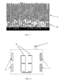
Fig. 1 shows a Scanning Electron Microscope micrograph of an exemplary coated cutting tool according to the present invention, in which- A) Ti-Si-C-N coating
- B) Cutting tool substrate
-
Fig. 2 shows schematically an exemplary target configuration of the arc evaporation equipment according to the present invention, in which- A) Titanium targets
- B) Substrate holders
- C) Vacuum system, gas inlet
- According to the present invention there is provided a cutting tool for metal machining, such as turning, milling and drilling, comprising a substrate of cemented carbide, cermet, ceramic or a super hard material, such as cubic boron nitride or diamond, preferably cemented carbide, and a hard and wear resistant refractory coating comprising a PVD Ti-Si-C-N layer.
- The thickness of the PVD Ti-Si-C-N layer is preferably chosen in a range common for PVD functional layers for metal cutting tools, i.e. suitably 1 to 10 µm, preferably 2 to 7 µm, most preferably 2 to 5 µm.
- The coating may include further layers such as e.g. a thin bonding layer between the substrate and the PVD Ti-Si-C-N layer, e.g. TiN, or an outermost layer for wear detection or colouring purposes, the total thickness of the deposited coating should, however, not exceed 11 µm, preferably not exceed 8 µm, to avoid spalling. In one embodiment the coating consists of a thin, preferably 0.2 to 1 µm thick, starting layer of, e.g., TiN, and a single Ti-Si-C-N functional layer, preferably 2 to 5 µm thick, possibly with a thin, preferably 0.2 to 1 µm thick, outermost colouring or wear detection layer of, e.g., TiN.
- The composition of the Ti-Si-C-N coating, when seen as Si in relation to Ti, i.e. the Si/(Si+Ti) atomic ratio, is suitably 0.03 to 0.25, preferably 0.045 to 0.22. It has been found that lower ratios results in loss in flank wear resistance, whereas higher ratios results in a too brittle layer leading to loss in crater wear resistance.
- The composition with regards C in relation to N, i.e. the C/(C+N) atomic ratio, is suitably 0.05 to 0.25, preferably 0.1 to 0.2. It has been found that below these values a decrease in hardness is obtained leading to unacceptable flank wear resistance. Too high C content, on the other hand, results in a too high residual compressive stress level and inferior cutting performance.
- It is also preferred that the residual stress of the Ti-Si-C-N layer, measured in the (220)-direction, is suitably from -3.0 GPa (compressive stress) up to +0.5 GPa (tensile stress).
- The hardness of the described Ti-Si-C-N coating can be in the range of 20 to 40 GPa. It has been found, however, that it is not possible to predict the performance in metal machining by studying the coating hardness. Results show that an increased hardness of the coating does not automatically lead to an increased wear resistance.
- In one embodiment of the present invention said PVD Ti-Si-C-N layer has a Si/(Si+Ti) atomic ratio of 0.05 to 0.15, and a residual stress of -2.0 GPa (compressive stress) up to +0.5 GPa (tensile stress). It has surprisingly been found that such a cutting tool combines both high resistance to crater wear and high resistance to flank wear.
- Exemplary metal cutting tools according to the invention are milling, turning, drilling or threading inserts, for clamping in a tool holder, but can also be in the form of a solid drill, a milling cutter or a threading tap.
- According to the present invention there is provided a method for making a cutting tool for metal machining, comprising depositing a hard and wear resistant refractory PVD Ti-Si-C-N layer, with the ability to control the incorporation of silicon content on a continuous scale and the ability to control the residual stress of the described Ti-Si-C-N coating on a continuous scale, onto a substrate of cemented carbide, cermet, ceramic or a super hard material, such as cubic boron nitride or diamond, preferably cemented carbide, by PVD arc evaporation technique combined with the addition of trimethylsilane gas during deposition.
- The PVD Ti-Si-C-N layer is preferably deposited to a thickness in a range common for PVD functional layers for metal cutting tools, i.e. suitably 1 to 10 µm, preferably 2 to 7 µm, most preferably 2 to 5 µm.
- In the arc evaporation process, for depositing the Ti-Si-C-N layer, one or more targets of Ti are used together with the addition of trimethylsilane gas, (CH3)3SiH, at a constant flow controlled by a mass flow controller. As an important feature this procedure allows for continuously controlling the material composition of the deposited coatings, specifically the Si concentration, and still making use of the benefits of the mentioned arc evaporation process. It is preferred that the added trimethylsilane gas is the sole source of Si in the deposition process.
- The deposition process is suitably performed at substrate temperatures between 400 to 600 °C. The base pressure prior to deposition should be <50 µPa and the Ar sputtering gas flow is suitably in the range 0 to 500 sccm. The reactive gas such as N2 and trimethylsilane is let in through a common inlet or through separate inlets. The N2 flow is suitably in the range of 500 to 1000 sccm.
- By varying the trimethylsilane gas flow it is possible to control the composition of the resulting coating, with regards to Si and C content.
- The substrates are connected by a potential difference to the deposition chamber wall, this potential referred to as the substrate bias. The substrate bias is suitably in the range of -50 to -150 V. By varying the substrate bias the residual stress of the resulting coatings is controlled; by an increase in the substrate bias the residual compressive stress is increased.
- Cemented carbide inserts of ISO-type CNMG120408 for turning, consisting of 10 wt-%Co, 0.39 wt-%Cr and balance WC with a hardness of 1600 HV3, were cleaned and subjected to a PVD coating process according to the following. The inserts were loaded into a reactive arc evaporation type PVD equipment chamber containing four metal evaporation sources, arranged in two pairs. The inserts were further subjected to a three-fold rotation in order to coat them homogeneously. The evaporation sources had all Ti targets. The chamber was evacuated, followed by the steps of heating and plasma etching in order to further clean the tools, and to condition their surfaces by removing excess binder phase from the insert surface. By metal evaporation whilst maintaining a partial pressure of nitrogen in the coater a thin TiN adhesion layer was deposited at a temperature of 450 °C. Next a wear resistant Ti-Si-C-N layer was deposited by arc evaporation of four Ti targets in a mixed Argon, Nitrogen and Trimethylsilane atmosphere. Argon was introduced in the process to avoid poisoning of the Ti-targets. It was found that an Argon flow of about 100-400 sccm was favourable, even though the process worked satisfactory also with zero Argon flow. The substrate bias level was chosen to obtain dense coatings with low compressive stresses. The deposition temperature of the wear resistant layer was 450 °C. The details are given in Table 1.
Table 1. Samples 1-4 (invention) Sample Time
[min.]Bias
[V]Ar
[sccm]N2
[sccm]Trimethylsilane
[sccm]1 120 -75 300 700 42 2 120 -90 100 700 125 3 120 -90 300 700 42 4 120 -125 300 700 83 - The results of the analyses of the different coatings are shown in Table 2.
- The Si/(Si+Ti) and C/(C+N) ratios were determined by Electron Probe Micro Analysis (EPMA). The average chemical composition was determined by EPMA using a JEOL JXA-8900R equipped with wavelength dispersive spectrometers at an acceleration voltage of 10 kV and a 10 nA probe current. Ti, Si and C contents were obtained by analysis while the N content was estimated by the difference between the sum of measured Ti, Si and C contents and 100 percent. The measurements were performed at the clearance side of the insert within 2 mm from the cutting edge.
- X-ray diffraction technique, more specifically the sin2 ψ method (I.C. Noyan, J.B. Cohen, Residual Stress Measurement by Diffraction and Interpretation, Springer-Verlag, New York, 1987 (pp 117-130)), was used for determining the residual stress in the wear resistant layer.
- A CSEM nano hardness tester was used to determine the hardness of the coatings. By using a load of 50 mN the contribution from the substrate was regarded as very small or none for all coatings.
- The crater and flank wear resistance were measured in two different turning applications.
- In the first test the crater wear resistance was evaluated. In this test the working material was a ball bearing steel. The cutting speed was 160 m/min. The feed was 0.3 mm/rev. and the cutting depth was 2.0 mm. The life time is defined as minutes in cut until the crater area becomes large enough to reach the cutting edge.
- In the second test the flank wear resistance was evaluated. In this case a nodular cast iron was used as working material. The cutting speed was 200 m/min. The feed was 0.1 mm/rev. and the cutting depth was 2.0 mm. The time in cut was 2 min. After that the insert was examined on the flank face and proportion of the cutting edge which was worn through was determined.
Table 2 Samples 1-4 (invention) Sample Thickness
[µm]Si/(Si+Ti)
RatioC/(C+N)
RatioResidual stress
[GPa]Hardness
[GPa]Crater Wear
[min.]Flank Wear
[%]1 3.5 0.049 0.151 -1.4 32 23 75 2 2.6 0.216 0.173 -0.1 24 7 0 3 3.0 0.052 0.108 -2.2 36 22 50 4 2.8 1 0.087 0.102 -2.8 39 22 100 - From Table 2 it is clear that it is possible to optimise the tool with regards its resistance to crater wear or flank wear.
- Inserts of the same composition and ISO-type as for Sample 1-4 were cleaned and subjected to a PVD coating process as described in Samples 1-4.
Table 3. Samples 5-10 (invention) Sample Time
[min.]Bias
[V]Ar
[sccm]N2
[sccm]Trimethylsilane
[sccm]5 120 -75 300 700 62 6 120 -75 300 700 83 7 120 -90 200 700 83 8 120 -75 0 700 83 9 120 -100 300 700 83 10 150 -75 300 700 66 Table 4. Results Samples 5-10 (invention) Sample Thickness
[µm]Si/(Si+Ti)
RatioC/(C+N)
RatioResidual stress
[GPa]Hardness
[GPa]Crater wear
[min.]Flank Wear
[%]5 3.3 0.089 0.147 -0.7 32 21 0 6 3.2 0.110 0.177 +0.3 29 13 0 7 2.6 0.131 0.130 -1.8 36 21 0 8 3.0 0.106 0.119 -2.0 - 22 0 9 2.8 0.138 0.156 -1.1 33 21 0 10 4.7 0.091 0.115 -0.8 - 24 0 - The Samples 5-10 in Table 4 show that it is possible to obtain for the same coating a both superior crater and flank wear resistance when the deposition parameters are carefully selected according to the present invention.
- Cemented carbide inserts of the same composition and ISO-type as for Samples 1-4 were coated according to two different coating schemes.
- Sample 11, being a commercially available state of the art grade particularly for applications demanding high crater wear resistance, such as turning of steel, was coated with a 4.1 µm PVD lamella layers with alternating layers of TiN and Al0.5Ti0.5N. The thickness of each individual TiN or Al0.5Ti0.5N -layer was 0.1-20 nm. The average composition of the multilayer was Al0.15Ti0.85N measured with SEM-EDS.
- Sample 12, being a commercially available state of the art grade particularly for hard work materials, such as HRSA and Inconel, was coated with a 3.9 µm PVD coating with composition Al0.67Ti0.33N as measured by SEM-EDS.
- Samples 11 and 12 were subjected to the same two machining tests as Samples 1-4 and the results are shown in Table 5.
Table 5. Results Samples 11 and 12 (Prior art) Sample Crater Wear
[min.]Flank Wea
[%]11 21 100 12 6 0 - Samples 11 and 12 represent cutting tool inserts particularly developed for applications demanding high crater wear resistance and high resistance to flank wear, respectively, which is also confirmed by the above results. Comparing these results with the results of embodiments of the invention according to Samples 5-10, Table 4, clearly shows the remarkable effect, wherein both high resistance to crater wear and high resistance to flank wear is combined in a single cutting tool.
Claims (9)
- A cutting tool for metal machining comprising a cutting tool substrate of cemented carbide, cermet, ceramics or a super hard material, and a wear resistant coating, characterized in that the wear resistant coating comprises a PVD Ti-Si-C-N layer.
- A cutting tool according to any of the preceding claims characterized in that said PVD Ti-Si-C-N layer has a Si/(Si+Ti) atomic ratio of 0.03 to 0.25.
- A cutting tool according to any of the preceding claims characterized in that said PVD Ti-Si-C-N layer has a residual stress of -3.0 GPa, compressive stress, up to +0.5 GPa, tensile stress.
- A cutting tool according to claim 1 characterized in that said PVD Ti-Si-C-N layer has a Si/(Si+Ti) atomic ratio of 0.05 to 0.15, and a residual stress of -2.0 GPa, compressive stress, up to +0.5 GPa, tensile stress.
- A cutting tool according to any of the preceding claims characterized in that said PVD Ti-Si-C-N layer has a C/(C+N) atomic ratio of 0.05 to 0.25.
- A cutting tool according to any of the preceding claims characterized in that said cutting tool substrate is of cemented carbide.
- A cutting tool according to any of the preceding claims characterized in that said tool is a cutting tool insert.
- A cutting tool according to any of the preceding claims characterized in that said tool is a solid drill, a milling cutter or a threading tap.
- Method of making a cutting tool for metal machining characterized by comprising depositing on to a cutting tool substrate of cemented carbide, cermet, ceramics or a super hard material, a PVD Ti-Si-C-N layer using arc evaporation with one or more Ti targets and an addition of trimethylsilane gas to the reactive gas atmosphere.
Applications Claiming Priority (1)
| Application Number | Priority Date | Filing Date | Title |
|---|---|---|---|
| SE0701028A SE530944C2 (en) | 2007-04-27 | 2007-04-27 | Notch |
Publications (2)
| Publication Number | Publication Date |
|---|---|
| EP1988190A2 true EP1988190A2 (en) | 2008-11-05 |
| EP1988190A3 EP1988190A3 (en) | 2011-08-03 |
Family
ID=39512773
Family Applications (1)
| Application Number | Title | Priority Date | Filing Date |
|---|---|---|---|
| EP08103610A Withdrawn EP1988190A3 (en) | 2007-04-27 | 2008-04-18 | Coated cutting tool |
Country Status (7)
| Country | Link |
|---|---|
| US (1) | US8105966B2 (en) |
| EP (1) | EP1988190A3 (en) |
| JP (1) | JP5087748B2 (en) |
| KR (1) | KR20080096470A (en) |
| CN (1) | CN101293773B (en) |
| IL (1) | IL191041A0 (en) |
| SE (1) | SE530944C2 (en) |
Cited By (10)
| Publication number | Priority date | Publication date | Assignee | Title |
|---|---|---|---|---|
| RU2430987C1 (en) * | 2010-04-13 | 2011-10-10 | Государственное образовательное учреждение высшего профессионального образования "Ульяновский государственный технический университет" | Procedure for production of multi-layer coating for cutting tool |
| EP2392688A1 (en) * | 2010-06-07 | 2011-12-07 | Sandvik Intellectual Property AB | Coated cutting tool |
| EP2276874A4 (en) * | 2008-04-18 | 2012-01-18 | Sandvik Intellectual Property | COATED CUTTING TOOL AND METHOD FOR MANUFACTURING THE SAME |
| WO2012047945A3 (en) * | 2010-10-05 | 2012-05-31 | Silcotek Corp. | Wear resistant coating, article, and method |
| US9340880B2 (en) | 2009-10-27 | 2016-05-17 | Silcotek Corp. | Semiconductor fabrication process |
| US11131020B2 (en) | 2015-09-01 | 2021-09-28 | Silcotek Corp. | Liquid chromatography system and component |
| US11292924B2 (en) | 2014-04-08 | 2022-04-05 | Silcotek Corp. | Thermal chemical vapor deposition coated article and process |
| US11618970B2 (en) | 2019-06-14 | 2023-04-04 | Silcotek Corp. | Nano-wire growth |
| US12036765B2 (en) | 2017-09-13 | 2024-07-16 | Silcotek Corp | Corrosion-resistant coated article and thermal chemical vapor deposition coating process |
| US12473635B2 (en) | 2020-06-03 | 2025-11-18 | Silcotek Corp. | Dielectric article |
Families Citing this family (15)
| Publication number | Priority date | Publication date | Assignee | Title |
|---|---|---|---|---|
| RU2415966C1 (en) * | 2009-11-30 | 2011-04-10 | Учреждение Российской академии наук Институт сильноточной электроники Сибирского отделения РАН | Procedure for coating items out of hard alloys |
| CA2778198C (en) | 2010-09-01 | 2014-09-09 | Sumitomo Electric Hardmetal Corp. | Cubic boron nitride sintered body tool |
| US9120707B2 (en) | 2010-10-18 | 2015-09-01 | Sumitomo Electric Hardmetal Corp. | Cubic boron nitride sintered body and cubic boron nitride sintered body tool |
| EP2631026B1 (en) * | 2010-10-19 | 2017-05-03 | Sumitomo Electric Hardmetal Corp. | Tool comprising sintered cubic boron nitride |
| CN102821898B (en) | 2010-10-27 | 2015-01-28 | 住友电工硬质合金株式会社 | Cubic boron nitride sintered body and cubic boron nitride sintered body tool |
| CN102731094B (en) * | 2012-06-11 | 2014-07-02 | 上海德宝密封件有限公司 | Silicon carbide-nano carbon tube composite toughened sealing wearing ring and preparation method thereof |
| CN102924086B (en) * | 2012-11-22 | 2013-12-11 | 山东轻工业学院 | Preparation method of h-BN added titanium boride-based self-lubricating ceramic cutter material |
| JP6039477B2 (en) * | 2013-03-23 | 2016-12-07 | 京セラ株式会社 | Cutting tools |
| JP5834329B2 (en) * | 2014-04-25 | 2015-12-16 | 住友電工ハードメタル株式会社 | Composite sintered body and surface-coated boron nitride sintered body tool |
| EP3221280B1 (en) | 2014-11-19 | 2019-09-25 | Diamond Innovations, Inc. | Method of preparing a multimodal cubic boron nitride powder |
| JP2017014084A (en) | 2015-07-03 | 2017-01-19 | 昭和電工株式会社 | Cubic crystal boron nitride sintered body, method of producing cubic crystal boron nitride sintered body, tool and cutting tool |
| DE112018001728T5 (en) * | 2017-03-30 | 2019-12-12 | Kyocera Corporation | CUTTING INSERT AND CUTTING TOOL |
| JP7730474B2 (en) * | 2020-03-13 | 2025-08-28 | 三菱マテリアル株式会社 | rigid composite material |
| CN115916438B (en) | 2020-06-30 | 2025-11-04 | 京瓷株式会社 | blades and cutting tools |
| CN116748531B (en) * | 2023-06-08 | 2025-12-23 | 西北有色金属研究院 | A method for preparing M2 high-speed steel cutting tools with gradient crystal structure |
Family Cites Families (15)
| Publication number | Priority date | Publication date | Assignee | Title |
|---|---|---|---|---|
| JPH0621314B2 (en) | 1985-12-28 | 1994-03-23 | 住友電気工業株式会社 | Sintered body for high hardness tool and manufacturing method thereof |
| JPH08197305A (en) | 1995-01-26 | 1996-08-06 | Mitsubishi Materials Corp | Cutting tool made of cubic boron nitride based ultra high pressure sintered material with high strength and toughness |
| US5639285A (en) * | 1995-05-15 | 1997-06-17 | Smith International, Inc. | Polycrystallline cubic boron nitride cutting tool |
| JPH10114575A (en) | 1996-10-04 | 1998-05-06 | Sumitomo Electric Ind Ltd | High hardness sintered body for tools |
| US6256337B1 (en) * | 1996-11-21 | 2001-07-03 | Dsp Group, Inc. | Rapid acquisition of PN synchronization in a direct-sequence spread-spectrum digital communications system |
| RU2220929C2 (en) | 1998-07-22 | 2004-01-10 | Сумитомо Электрик Индастриз, Лтд. | Sintered blanc from boron nitride with cubic lattice (options) |
| US6265337B1 (en) | 1998-12-04 | 2001-07-24 | Sumitomo Electric Industries, Ltd. | High strength sintered body |
| WO2003061884A1 (en) * | 2002-01-21 | 2003-07-31 | Mitsubishi Materials Kobe Tools Corporation | Surface coated cutting tool member having hard coating layer exhibiting excellent abrasion resistance in high-speed cutting, and method for forming said hard coating layer on surface of cutting tool |
| EP1498199B1 (en) | 2002-04-19 | 2010-08-18 | Mitsubishi Materials Corporation | Cubic boron nitride base ultra-high pressure sintered material cutting tip |
| CN100488710C (en) | 2003-06-03 | 2009-05-20 | 山特维克知识产权股份有限公司 | Indexable cutter and methods for producing the same |
| JP4405835B2 (en) | 2004-03-18 | 2010-01-27 | 住友電工ハードメタル株式会社 | Surface coated cutting tool |
| JP4704335B2 (en) * | 2004-03-18 | 2011-06-15 | 住友電工ハードメタル株式会社 | Surface coated cutting tool |
| KR101226422B1 (en) | 2004-10-29 | 2013-01-24 | 엘리먼트 씩스 (프로덕션) (피티와이) 리미티드 | Cubic boron nitride compact |
| SE529290C2 (en) | 2005-10-28 | 2007-06-19 | Sandvik Intellectual Property | Cut off cubic boron nitride resistant to chipping and breaking |
| KR20100015344A (en) * | 2007-04-18 | 2010-02-12 | 산드빅 인터렉츄얼 프로퍼티 에이비 | A coated cutting tool and a method of making thereof |
-
2007
- 2007-04-27 SE SE0701028A patent/SE530944C2/en not_active IP Right Cessation
-
2008
- 2008-04-18 EP EP08103610A patent/EP1988190A3/en not_active Withdrawn
- 2008-04-18 US US12/081,638 patent/US8105966B2/en not_active Expired - Fee Related
- 2008-04-24 JP JP2008114385A patent/JP5087748B2/en not_active Expired - Fee Related
- 2008-04-25 KR KR1020080038939A patent/KR20080096470A/en not_active Ceased
- 2008-04-27 IL IL191041A patent/IL191041A0/en unknown
- 2008-04-28 CN CN2008100923957A patent/CN101293773B/en not_active Expired - Fee Related
Non-Patent Citations (4)
| Title |
|---|
| H. XU ET AL., SURFACE & COATINGS TECHNOLOGY, vol. 201, 2006, pages 4236 - 4241 |
| I.C. NOYAN; J.B. COHEN: "Residual Stress Measurement by Diffraction and Interpretation", 1987, SPRINGER-VERLAG, pages: 117 - 130 |
| JEON ET AL., SURFACE AND COATINGS TECHNOLOGY, vol. 188-189, 2004, pages 415 - 419 |
| MA ET AL., THIN SOLID FILMS, vol. 496, 2006, pages 438 - 444 |
Cited By (20)
| Publication number | Priority date | Publication date | Assignee | Title |
|---|---|---|---|---|
| US8507110B2 (en) | 2008-04-18 | 2013-08-13 | Sandvik Intellectual Property Ab | Coated cutting tool and a method of making thereof |
| EP2276874A4 (en) * | 2008-04-18 | 2012-01-18 | Sandvik Intellectual Property | COATED CUTTING TOOL AND METHOD FOR MANUFACTURING THE SAME |
| US9340880B2 (en) | 2009-10-27 | 2016-05-17 | Silcotek Corp. | Semiconductor fabrication process |
| RU2430987C1 (en) * | 2010-04-13 | 2011-10-10 | Государственное образовательное учреждение высшего профессионального образования "Ульяновский государственный технический университет" | Procedure for production of multi-layer coating for cutting tool |
| CN102985583A (en) * | 2010-06-07 | 2013-03-20 | 山特维克知识产权股份有限公司 | Coated cutting tool |
| US9157143B2 (en) | 2010-06-07 | 2015-10-13 | Sandvik Intellectual Property | Coated cutting tool |
| WO2011154291A1 (en) * | 2010-06-07 | 2011-12-15 | Sandvik Intellectual Property Ab | Coated cutting tool |
| CN102985583B (en) * | 2010-06-07 | 2015-04-08 | 山特维克知识产权股份有限公司 | Coated cutting tool |
| EP2392688A1 (en) * | 2010-06-07 | 2011-12-07 | Sandvik Intellectual Property AB | Coated cutting tool |
| US10604660B2 (en) | 2010-10-05 | 2020-03-31 | Silcotek Corp. | Wear resistant coating, article, and method |
| KR101512579B1 (en) * | 2010-10-05 | 2015-04-15 | 실코텍 코포레이션 | Wear resistant coating, article, and method |
| WO2012047945A3 (en) * | 2010-10-05 | 2012-05-31 | Silcotek Corp. | Wear resistant coating, article, and method |
| US12522732B2 (en) | 2010-10-05 | 2026-01-13 | Silcotek Corp. | Amorphous coating |
| US11292924B2 (en) | 2014-04-08 | 2022-04-05 | Silcotek Corp. | Thermal chemical vapor deposition coated article and process |
| US11131020B2 (en) | 2015-09-01 | 2021-09-28 | Silcotek Corp. | Liquid chromatography system and component |
| US12037685B2 (en) | 2015-09-01 | 2024-07-16 | Silcotek Corp | Liquid chromatography system and component |
| US12291778B2 (en) | 2015-09-01 | 2025-05-06 | Silcotek Corp. | Liquid chromatography system and component |
| US12036765B2 (en) | 2017-09-13 | 2024-07-16 | Silcotek Corp | Corrosion-resistant coated article and thermal chemical vapor deposition coating process |
| US11618970B2 (en) | 2019-06-14 | 2023-04-04 | Silcotek Corp. | Nano-wire growth |
| US12473635B2 (en) | 2020-06-03 | 2025-11-18 | Silcotek Corp. | Dielectric article |
Also Published As
| Publication number | Publication date |
|---|---|
| KR20080096470A (en) | 2008-10-30 |
| JP5087748B2 (en) | 2012-12-05 |
| SE0701028L (en) | 2008-10-28 |
| EP1988190A3 (en) | 2011-08-03 |
| US20080264203A1 (en) | 2008-10-30 |
| CN101293773B (en) | 2012-12-12 |
| SE530944C2 (en) | 2008-10-28 |
| CN101293773A (en) | 2008-10-29 |
| IL191041A0 (en) | 2008-12-29 |
| US8105966B2 (en) | 2012-01-31 |
| JP2008272929A (en) | 2008-11-13 |
Similar Documents
| Publication | Publication Date | Title |
|---|---|---|
| EP2147132B1 (en) | A coated cutting tool | |
| EP2276874B1 (en) | A coated cutting tool and a method of making thereof | |
| JP3996809B2 (en) | Coated cutting tool | |
| EP1710326B1 (en) | Surface-coated cutting tool | |
| EP3269479A1 (en) | Surface-coated cutting tool and manufacturing method therefor | |
| CN111587157B (en) | Surface-coated cutting tool and method for manufacturing same | |
| KR20130115225A (en) | Cutting tool | |
| KR20160088351A (en) | Coated tool | |
| KR101635486B1 (en) | Cutting tool | |
| JPWO2019171653A1 (en) | Surface coating cutting tool and its manufacturing method | |
| CN112805109A (en) | Cutting tool and method for manufacturing same | |
| JP7486045B2 (en) | Surface-coated cutting tools | |
| JP7055961B2 (en) | Surface coating cutting tool and its manufacturing method | |
| JP6743349B2 (en) | Cutting tools | |
| CN119384329A (en) | Cutting Tools | |
| CN112262007B (en) | cutting tool | |
| JP7409554B1 (en) | Cutting tools | |
| WO2024062613A9 (en) | Cutting tool | |
| CN120051345A (en) | Cutting tool |
Legal Events
| Date | Code | Title | Description |
|---|---|---|---|
| PUAI | Public reference made under article 153(3) epc to a published international application that has entered the european phase |
Free format text: ORIGINAL CODE: 0009012 |
|
| AK | Designated contracting states |
Kind code of ref document: A2 Designated state(s): AT BE BG CH CY CZ DE DK EE ES FI FR GB GR HR HU IE IS IT LI LT LU LV MC MT NL NO PL PT RO SE SI SK TR |
|
| AX | Request for extension of the european patent |
Extension state: AL BA MK RS |
|
| PUAL | Search report despatched |
Free format text: ORIGINAL CODE: 0009013 |
|
| AK | Designated contracting states |
Kind code of ref document: A3 Designated state(s): AT BE BG CH CY CZ DE DK EE ES FI FR GB GR HR HU IE IS IT LI LT LU LV MC MT NL NO PL PT RO SE SI SK TR |
|
| AX | Request for extension of the european patent |
Extension state: AL BA MK RS |
|
| RIC1 | Information provided on ipc code assigned before grant |
Ipc: C23C 14/32 20060101ALI20110630BHEP Ipc: C23C 30/00 20060101ALI20110630BHEP Ipc: C23C 28/04 20060101ALI20110630BHEP Ipc: C23C 28/00 20060101AFI20110630BHEP |
|
| 17P | Request for examination filed |
Effective date: 20120203 |
|
| AKX | Designation fees paid |
Designated state(s): AT BE BG CH CY CZ DE DK EE ES FI FR GB GR HR HU IE IS IT LI LT LU LV MC MT NL NO PL PT RO SE SI SK TR |
|
| STAA | Information on the status of an ep patent application or granted ep patent |
Free format text: STATUS: THE APPLICATION IS DEEMED TO BE WITHDRAWN |
|
| 18D | Application deemed to be withdrawn |
Effective date: 20120204 |