EP1983371A1 - Stage apparatus, exposure apparatus, and device manufacturing method - Google Patents
Stage apparatus, exposure apparatus, and device manufacturing method Download PDFInfo
- Publication number
- EP1983371A1 EP1983371A1 EP08153901A EP08153901A EP1983371A1 EP 1983371 A1 EP1983371 A1 EP 1983371A1 EP 08153901 A EP08153901 A EP 08153901A EP 08153901 A EP08153901 A EP 08153901A EP 1983371 A1 EP1983371 A1 EP 1983371A1
- Authority
- EP
- European Patent Office
- Prior art keywords
- stage
- reticle
- holding unit
- moving stage
- length
- Prior art date
- Legal status (The legal status is an assumption and is not a legal conclusion. Google has not performed a legal analysis and makes no representation as to the accuracy of the status listed.)
- Granted
Links
Images








Classifications
-
- G—PHYSICS
- G03—PHOTOGRAPHY; CINEMATOGRAPHY; ANALOGOUS TECHNIQUES USING WAVES OTHER THAN OPTICAL WAVES; ELECTROGRAPHY; HOLOGRAPHY
- G03F—PHOTOMECHANICAL PRODUCTION OF TEXTURED OR PATTERNED SURFACES, e.g. FOR PRINTING, FOR PROCESSING OF SEMICONDUCTOR DEVICES; MATERIALS THEREFOR; ORIGINALS THEREFOR; APPARATUS SPECIALLY ADAPTED THEREFOR
- G03F7/00—Photomechanical, e.g. photolithographic, production of textured or patterned surfaces, e.g. printing surfaces; Materials therefor, e.g. comprising photoresists; Apparatus specially adapted therefor
- G03F7/70—Microphotolithographic exposure; Apparatus therefor
- G03F7/70691—Handling of masks or workpieces
- G03F7/70783—Handling stress or warp of chucks, masks or workpieces, e.g. to compensate for imaging errors or considerations related to warpage of masks or workpieces due to their own weight
-
- G—PHYSICS
- G03—PHOTOGRAPHY; CINEMATOGRAPHY; ANALOGOUS TECHNIQUES USING WAVES OTHER THAN OPTICAL WAVES; ELECTROGRAPHY; HOLOGRAPHY
- G03F—PHOTOMECHANICAL PRODUCTION OF TEXTURED OR PATTERNED SURFACES, e.g. FOR PRINTING, FOR PROCESSING OF SEMICONDUCTOR DEVICES; MATERIALS THEREFOR; ORIGINALS THEREFOR; APPARATUS SPECIALLY ADAPTED THEREFOR
- G03F7/00—Photomechanical, e.g. photolithographic, production of textured or patterned surfaces, e.g. printing surfaces; Materials therefor, e.g. comprising photoresists; Apparatus specially adapted therefor
- G03F7/70—Microphotolithographic exposure; Apparatus therefor
- G03F7/70691—Handling of masks or workpieces
- G03F7/70716—Stages
-
- G—PHYSICS
- G03—PHOTOGRAPHY; CINEMATOGRAPHY; ANALOGOUS TECHNIQUES USING WAVES OTHER THAN OPTICAL WAVES; ELECTROGRAPHY; HOLOGRAPHY
- G03F—PHOTOMECHANICAL PRODUCTION OF TEXTURED OR PATTERNED SURFACES, e.g. FOR PRINTING, FOR PROCESSING OF SEMICONDUCTOR DEVICES; MATERIALS THEREFOR; ORIGINALS THEREFOR; APPARATUS SPECIALLY ADAPTED THEREFOR
- G03F7/00—Photomechanical, e.g. photolithographic, production of textured or patterned surfaces, e.g. printing surfaces; Materials therefor, e.g. comprising photoresists; Apparatus specially adapted therefor
- G03F7/70—Microphotolithographic exposure; Apparatus therefor
- G03F7/70691—Handling of masks or workpieces
- G03F7/707—Chucks, e.g. chucking or un-chucking operations or structural details
-
- G—PHYSICS
- G03—PHOTOGRAPHY; CINEMATOGRAPHY; ANALOGOUS TECHNIQUES USING WAVES OTHER THAN OPTICAL WAVES; ELECTROGRAPHY; HOLOGRAPHY
- G03F—PHOTOMECHANICAL PRODUCTION OF TEXTURED OR PATTERNED SURFACES, e.g. FOR PRINTING, FOR PROCESSING OF SEMICONDUCTOR DEVICES; MATERIALS THEREFOR; ORIGINALS THEREFOR; APPARATUS SPECIALLY ADAPTED THEREFOR
- G03F7/00—Photomechanical, e.g. photolithographic, production of textured or patterned surfaces, e.g. printing surfaces; Materials therefor, e.g. comprising photoresists; Apparatus specially adapted therefor
- G03F7/70—Microphotolithographic exposure; Apparatus therefor
- G03F7/708—Construction of apparatus, e.g. environment aspects, hygiene aspects or materials
- G03F7/70808—Construction details, e.g. housing, load-lock, seals or windows for passing light in or out of apparatus
-
- H—ELECTRICITY
- H10—SEMICONDUCTOR DEVICES; ELECTRIC SOLID-STATE DEVICES NOT OTHERWISE PROVIDED FOR
- H10P—GENERIC PROCESSES OR APPARATUS FOR THE MANUFACTURE OR TREATMENT OF DEVICES COVERED BY CLASS H10
- H10P72/00—Handling or holding of wafers, substrates or devices during manufacture or treatment thereof
- H10P72/70—Handling or holding of wafers, substrates or devices during manufacture or treatment thereof for supporting or gripping
Definitions
- the present invention relates to a stage apparatus which holds a reticle (original) in, for example, an exposure apparatus, an exposure apparatus, and a device manufacturing method.
- An exposure apparatus for manufacturing a semiconductor device has a reticle stage and wafer stage for aligning a reticle (mask) as an original and a wafer as a substrate.
- a method of providing a coarse moving stage which moves with a large stroke and a fine moving stage which moves with a small stroke to the apparatus is disclosed in each of Japanese Patent Laid-Open No. 2000-106344 and " Ultraprecision Manufacturing Technology, Vol. 3; Technology of Measurement and Control" (first edition, Jul. 15, 1995, issued by Fuji Technosystem, pp. 20 - 27, supervised by Akira Kobayashi ).
- Figs. 8A and 8B are views showing a stage apparatus having coarse and fine moving mechanisms described in Japanese Patent Laid-Open No. 2000-106344 .
- a support frame (coarse moving stage) 306 connected to a feed screw system movable unit 311 for moving it with a large stroke can move on a plane guide 302.
- the support frame 306 has linear motor stators 305 for moving a stage (fine moving stage) 301 having linear motor movable elements 304 with a small stroke.
- the support frame 306 generates, together with the stage 301, a force which allows the stage 301 to move finely relative to the support frame 306.
- the support frame 306 also has a pair of electromagnets 308 which sandwich the stage 301 in the Y-axis direction. Each electromagnet 308 functions as an electromagnetic coupling by generating an attraction force together with a magnetic plate 307 provided to the stage 301. As the support frame 306 accelerates/decelerates with a high acceleration/deceleration, it transmits an acceleration/deceleration force to the stage 301 using the attraction force of one of the pair of electromagnets 308.
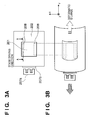
- Figs. 3A and 3B are views showing deformation of a fine moving stage 202 upon accelerating/decelerating it.
- Fig. 3A shows the state of the fine moving stage 202 before acceleration/deceleration.
- Fig. 3B shows the state in which a coarse moving stage 203 moves in the -Y direction with acceleration/deceleration to apply an acceleration/deceleration force to the fine moving stage 202 in the -Y direction.
- Figs. 3A and 3B do not illustrate any electromagnets which are not involved in the force application.
- the fine moving stage 202 deforms to extend mainly in the Y-axis direction upon receiving the force.
- Fig. 4 is a side view for explaining the section (A - A section) of Fig. 3A in the scanning direction while the reticle holding unit 208 fixed on the fine moving stage 202 holds and aligns a reticle 201 in Fig. 3A .
- Deformation of the fine moving stage 202 upon accelerating/decelerating it is transmitted to the reticle 201 via the reticle holding unit 208.
- Deformation of the reticle 201 makes it difficult to accurately transfer a reticle pattern drawn on it onto a silicon wafer.
- each electromagnetic coupling transmits a force to the fine moving stage using an attraction force.
- the fine moving stage is pulled by a large force from one side in one direction, it deforms and the reticle (mask) held by it also deforms.
- These deformations pose a serious problem especially in a stage apparatus for an exposure apparatus which is required to have a position reproducibility and allowable deformation amount on the order of nanometers.
- the present invention in its one aspect provides a stage apparatus as specified in claims 1 to 4 and 6.
- Fig. 1 is a view showing the entire arrangement of an exposure apparatus
- Fig. 2 is a view showing a reticle stage
- Figs. 3A and 3B are plan views showing deformation of a fine moving stage according to a prior art
- Fig. 4 is a side view of Fig. 3A ;
- Fig. 5A is a side view showing an example of a fine moving stage according to the present invention.
- Fig. 5B is a side view showing another example of the fine moving stage according to the present invention.
- Fig. 5C is a partial enlarged view of Fig. 5A ;
- Figs. 6A and 6B are plan views showing deformation of the fine moving stage
- Figs. 7A and 7B are a plan view and side view showing an arrangement which supports an original (reticle) at three points;
- Figs. 8A and 8B are views showing a stage apparatus according to a prior art
- Fig. 9 is a flowchart for explaining the device manufacture using an exposure apparatus.
- Fig. 10 is a flowchart illustrating details of the wafer process in step S4 of the flowchart shown in Fig. 9 .
- Fig. 1 is a view showing the entire apparatus according to an embodiment in which an exemplary stage apparatus according to the present invention is applied to an original stage (reticle stage) of an exposure apparatus.
- An illumination optical system 1 shapes exposure light emitted by a light source into uniform exposure light.
- a reticle stage 2 mounts an original (reticle) 6 and exposes the reticle 6 by scanning relative to the exposure light.
- a projection optical system 3 projects and transfers the pattern on the reticle 6 onto a wafer formed by a silicon substrate.
- a wafer stage 4 mounts a wafer as a silicon substrate and moves it by scanning relative to the exposure light in synchronism with the reticle stage 2.
- An exposure apparatus main body 5 supports, for example, the reticle stage 2, projection optical system 3, and wafer stage 4.
- a projection pattern is formed on the reticle 6.
- Fig. 2 is a view showing the reticle stage 2 according to this embodiment.
- the reticle stage 2 can have a coarse moving stage 203 and fine moving stage 202.
- the coarse moving stage 203 is supported to be movable on the upper surface of a base 204, and can be moved with a large stroke in the Y-axis direction as the scanning direction by a coarse movement linear motor 206.
- the coarse movement linear motor 206 has a stator and movable element.
- the stator includes a coil unit (not shown) supported by the base.
- the movable element includes a magnet unit fixed on the coarse moving stage 203.
- a Lorentz force is generated between the stator and the movable element to drive the coarse moving stage 203.
- the driving mechanism of the coarse moving stage 203 is not particularly limited to a linear motor, and may be of another type.
- the coarse moving stage 203 has, at its central portion, an opening 210 which propagates exposure light.
- the fine moving stage 202 which mounts a reticle 201 is inserted in the opening 210 and supported with low rigidity from the coarse moving stage 203 via a spring mechanism (including, for example, an air bearing; not shown).
- a fine movement linear motor 205 and electromagnetic couplings 207 are interposed between the fine moving stage 202 and the coarse moving stage 203.
- the fine movement linear motor 205 can finely move the fine moving stage 202 relative to the coarse moving stage 203.
- the fine movement linear motor 205 drives the fine moving stage 202 in a non-contact manner using the Lorentz force between the coil and the magnet, as exemplified in the prior art.
- the fine movement linear motor 205 can be arranged so as to finely drive the fine moving stage 202 in three axial directions, i.e., in the X direction, Y (scanning) direction, and Z (vertical) direction.
- the fine movement linear motor 205 can also be arranged so as to finely drive the fine moving stage 202 in six axial directions including three rotation directions about the X-, Y-, and Z-axes, in addition to the above-described directions.
- the number of axes and axial directions may be freely changed in accordance with design details such as the required precision and space.
- a laser interferometer 211 measures the position of the fine moving stage 202 in three axial directions or six axial directions.
- Each electromagnetic coupling 207 has, for example, an I core 207a as a magnetic material attached on the fine moving stage 202, an E core 207b as a magnetic material attached on the coarse moving stage 203, and an electromagnetic coupling coil 209 wound around the E core 207b.
- Reticle holding units 208 each are fixed on the fine moving stage 202 and made of a material identical to or different from that of the fine moving stage 202.
- This material is an elastically deformable member.
- the elastically deformable member here includes general elastic metal and resin materials, and general fragile glass and ceramic materials.
- Each reticle holding unit 208 has a chucking mechanism for holding and aligning the reticle 201, and a measurement light transmission hole for aligning the reticle 201. More specifically, light from a light emitting unit (not shown) irradiates the reticle 201 from above, is transmitted through a mark formed on the reticle 201, propagates through a measurement light transmission hole, and enters a light-receiving unit provided under the fine moving stage 202.
- the light-receiving unit comprises, for example, a camera sensor, which allows for detecting the relative position between the reticle 201 and the light-receiving unit.
- the fine moving stage is moved so that a reference mark formed on it falls within the detection range of the light-receiving unit, thereby detecting the relative position between the reference mark and the light-receiving unit.
- This makes it possible to obtain information on the relative positional shift between the reticle 201 and the fine moving stage 202 from the movement amount of the stage measured by the interferometer and the relative position between the light-receiving unit and each mark.
- the resultant relative position shift information can be reflected in the driving of the fine moving stage 202.
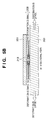
- Fig. 5A is a side view for explaining the section (B - B section) of Fig. 6A in the scanning direction while the reticle holding unit 208 fixed on the fine moving stage 202 holds the reticle 201.
- the reticle holding unit 208 is fixed on the fine moving stage 202 to extend in a first direction in which the fine moving stage 202 moves.
- the reticle holding unit 208 includes a first portion having a holding surface which holds a reticle (object), a second portion inserted between the first portion and the fine moving stage 202, and a third portion inserted between the second portion and the fine moving stage 202.
- the second portion is an elastic hinge portion which connects the first portion to the third portion via elastic hinges.
- the reticle holding unit 208 includes the third portion in this embodiment, it need not necessarily include the third portion.
- the fine moving stage 202 deforms upon receiving an acceleration/deceleration force.
- elastic hinges 213 provided in the same direction as the deformation direction of the fine moving stage 202 suppress deformation of the fine moving stage 202 from being transmitted to the reticle 201.
- the elastic hinges 213 suppress heat generated by the fine moving stage 202 from being transferred to the reticle 201.
- Fig. 5B shows a modification of the reticle holding unit 208.
- Fig. 5C is a partial enlarged view of the elastic hinges 213 shown in Fig. 5A , for explaining the state in which the elastic hinges 213 suppress deformation of the fine moving stage 202 from being transmitted to the reticle 201.
- Deformation of the fine moving stage 202 is transmitted to the reticle holding unit 208 due to friction between them.
- the elastic hinges 213 reduce the deformation of the reticle holding unit 208 transmitted to the reticle 201 to be smaller than the original deformation of the fine moving stage 202.
- An effect of suppressing the reticle holding unit 208 from deforming due to deformation of the fine moving stage 202 as described above can be controlled by changing the size of the elastic hinge portion of the reticle holding unit 208. More specifically, assume that the reticle holding unit 208 deforms by 100 nm due to deformation of the fine moving stage 202 upon accelerating/decelerating it with a certain acceleration. If the allowable deformation amount of the reticle 201 is 10 nm, the elastic hinges 213 in the reticle holding unit 208 reduce its deformation to 1/10.
- the deformation of the reticle 201 it is possible to reduce the deformation of the reticle 201 to 1/10 by adjusting the ratio between the sizes of the elastic hinge 213 and reticle holding unit 208 to a deformation reduction ratio (in this example, 1/10).
- a deformation reduction ratio in this example, 1/10.
- the reticle holding unit 208 has a size of 130 mm
- this deformation is directly transmitted to the reticle. That is, it is possible to suppress the deformation of the reticle 201 by adjusting the length of the second portion in the first direction, in which the fine moving stage 202 moves, to be less than that of the third portion.
- the length of the second portion is 10% of the lengths of the first portion and third portion in the above-described arrangement
- the length ratio of the second portion can be changed by taking account of a reticle deformation suppression action and stable reticle holding action. For example, even when the length of the second portion is adjusted to 70% or less of the lengths of the first portion and third portion by attaching importance to stable reticle holding, the reticle deformation can be suppressed sufficiently.
- the length ratio of the second portion is desirably 50% or less and, more desirably, 30% or less.
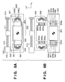
- Figs. 6A and 6B are plan views for explaining deformation of the fine moving stage 202 upon accelerating/decelerating it.
- Fig. 6A shows the state of the fine moving stage 202 before acceleration/deceleration.
- Fig. 6B shows the state in which the coarse moving stage 203 moves in the -Y direction with acceleration/deceleration to apply an acceleration/deceleration force to the fine moving stage 202 in the -Y direction.
- Figs. 6A and 6B do not illustrate any electromagnets which are not involved in the force application.
- the fine moving stage 202 deforms to extend mainly in the Y-axis direction upon receiving the force. However, the deformation of the reticle 201 is suppressed by an effect of suppressing deformation of the reticle holding unit 208 in its elastic hinge portion (second portion).
- reticle holding units 208 are separately provided in a plurality of portions on the fine moving stage 202, and can support the reticle 201 at three points on the fine moving stage 202.
- the linear expansion coefficient of the low-thermal expansion material is preferably 0.7 ppm/°C or less around 23°C and, more preferably, 0.1 ppm/°C or less for more effective deformation suppression.
- the stage apparatus according to this embodiment is applicable not only to a reticle stage but also to a high-precision stage apparatus. Although an arrangement in which a coarse moving stage coarsely moves in the scanning direction as one axial direction has been exemplified above, an arrangement in which it coarsely moves in two axial directions may be adopted. As a concrete example, the stage apparatus according to this embodiment is applicable to a wafer stage similarly built in an exposure apparatus.
- the exposure apparatus projects and transfers by exposure a circuit pattern formed on a reticle onto a wafer, and may adopt a step & repeat projection exposure scheme or step & scan projection exposure scheme.
- the illumination optical system 1 illuminates a reticle on which a circuit pattern is formed, and has a light source unit and illumination system.
- the light source unit uses, for example, a laser as a light source.
- the laser can be, for example, an ArF excimer laser with a wavelength of about 193 nm, a KrF excimer laser with a wavelength of about 248 nm, or an F 2 excimer laser with a wavelength of about 153 nm.
- the type of laser is not particularly limited to an excimer laser, and may be, for example, a YAG laser.
- the number of lasers used is not particularly limited as well.
- a laser is used as the light source, a light beam shaping optical system which shapes a collimated light beam from the laser light source into a desired beam shape, and an incoherent optical system which converts a coherent laser light beam into an incoherent light beam are preferably used.
- the light source which can be used for the light source unit is not particularly limited to a laser. It is also possible to use one or a plurality of lamps such as a mercury lamp or xenon lamp.
- the illumination optical system 1 illuminates a mask and includes, for example, a lens, mirror, light integrator, and stop.
- the projection optical system 3 can be, for example, an optical system including a plurality of lens elements alone, an optical system (catadioptric system) including a plurality of lens elements and a concave mirror, an optical system including a plurality of lens elements and a diffractive optical element such as kinoform, or an optical system including a total reflection mirror.
- the reticle stage 2 and wafer stage 4 can be moved by, for example, a linear motor.
- the stages 2 and 4 move in synchronism with each other.
- An actuator is separately provided to at least one of the wafer stage 4 and reticle stage 2 to align the pattern of the reticle 6 onto the wafer.
- Such an exposure apparatus can be used to manufacture a device, on which a micropattern is formed, for example, a semiconductor device such as a semiconductor integrated circuit, a micromachine, or a thin film magnetic head.
- Applying the alignment apparatus according to this embodiment to an exposure apparatus makes it possible to provide an exposure apparatus which attains high precision and high throughput by suppressing deterioration in precision due to the influence of deformation of a fine moving stage.
- FIG. 9 is a flowchart for explaining the manufacture of a device (for example, a semiconductor chip such as an IC or LSI, an LCD, or a CCD). A method of manufacturing a semiconductor chip will be exemplified here.
- step S1 circuit design
- step S2 mask fabrication
- step S3 wafer manufacture
- step S4 wafer process
- step S5 wafer process
- step S5 semiconductor chip is formed using the wafer manufactured in step S4. This step includes an assembly step (dicing and bonding) and packaging step (chip encapsulation).
- step S6 inspection
- the semiconductor device manufactured in step S5 undergoes inspections such as an operation confirmation test and durability test. After these steps, the semiconductor device is completed and shipped in step S7.
- Fig. 10 is a flowchart illustrating details of the wafer process in step S4.
- step S11 oxidation
- step S12 CVD
- step S13 electrode formation
- step S14 ion implantation
- step S15 resist processing
- step S16 exposure
- step S17 development
- step S18 etching
- step S19 resist removal
- the exposure apparatus according to this embodiment is used for exposure in such a device manufacturing process, it is possible to produce a device with high precision or high throughput and, consequently, to manufacture a microdevice and/or inexpensive device.
- This invention discloses a stage apparatus which has a stage (202) and moves the stage (202) in at least a first direction.
- the stage apparatus includes a holding unit (208) fixed on the stage (202) to extend in the first direction.
- the holding unit (208) includes a first portion and a second portion (213) inserted between the first portion and the stage (202).
- the first portion includes a holding surface which holds an object (201).
- the length of the second portion (213) in the first direction is less than that of the first portion.
Landscapes
- Physics & Mathematics (AREA)
- General Physics & Mathematics (AREA)
- Health & Medical Sciences (AREA)
- Engineering & Computer Science (AREA)
- Environmental & Geological Engineering (AREA)
- Epidemiology (AREA)
- Public Health (AREA)
- Exposure And Positioning Against Photoresist Photosensitive Materials (AREA)
- Container, Conveyance, Adherence, Positioning, Of Wafer (AREA)
- Exposure Of Semiconductors, Excluding Electron Or Ion Beam Exposure (AREA)
Abstract
Description
- The present invention relates to a stage apparatus which holds a reticle (original) in, for example, an exposure apparatus, an exposure apparatus, and a device manufacturing method.
- An exposure apparatus for manufacturing a semiconductor device has a reticle stage and wafer stage for aligning a reticle (mask) as an original and a wafer as a substrate. To attain high-precision alignment in such an alignment stage apparatus, a method of providing a coarse moving stage which moves with a large stroke and a fine moving stage which moves with a small stroke to the apparatus is disclosed in each of Japanese Patent Laid-Open No.
2000-106344 -
Figs. 8A and 8B are views showing a stage apparatus having coarse and fine moving mechanisms described in Japanese Patent Laid-Open No.2000-106344 movable unit 311 for moving it with a large stroke can move on aplane guide 302. Thesupport frame 306 haslinear motor stators 305 for moving a stage (fine moving stage) 301 having linear motormovable elements 304 with a small stroke. Thesupport frame 306 generates, together with thestage 301, a force which allows thestage 301 to move finely relative to thesupport frame 306. - The
support frame 306 also has a pair ofelectromagnets 308 which sandwich thestage 301 in the Y-axis direction. Eachelectromagnet 308 functions as an electromagnetic coupling by generating an attraction force together with amagnetic plate 307 provided to thestage 301. As thesupport frame 306 accelerates/decelerates with a high acceleration/deceleration, it transmits an acceleration/deceleration force to thestage 301 using the attraction force of one of the pair ofelectromagnets 308. -
Figs. 3A and 3B are views showing deformation of a fine movingstage 202 upon accelerating/decelerating it.Fig. 3A shows the state of the fine movingstage 202 before acceleration/deceleration.Fig. 3B shows the state in which a coarse movingstage 203 moves in the -Y direction with acceleration/deceleration to apply an acceleration/deceleration force to the fine movingstage 202 in the -Y direction.Figs. 3A and 3B do not illustrate any electromagnets which are not involved in the force application. The fine movingstage 202 deforms to extend mainly in the Y-axis direction upon receiving the force. -
Fig. 4 is a side view for explaining the section (A - A section) ofFig. 3A in the scanning direction while thereticle holding unit 208 fixed on the fine movingstage 202 holds and aligns areticle 201 inFig. 3A . Deformation of the fine movingstage 202 upon accelerating/decelerating it is transmitted to thereticle 201 via thereticle holding unit 208. As deformation of the fine movingstage 202 upon accelerating/decelerating it is transmitted to thereticle 201, it becomes impossible to attain high-precision alignment. Deformation of thereticle 201 makes it difficult to accurately transfer a reticle pattern drawn on it onto a silicon wafer. - In recent years, a demand has arisen for a stage apparatus with a higher precision. For example, as shown in
Fig. 3A , assume that each electromagnetic coupling transmits a force to the fine moving stage using an attraction force. When the fine moving stage is pulled by a large force from one side in one direction, it deforms and the reticle (mask) held by it also deforms. These deformations pose a serious problem especially in a stage apparatus for an exposure apparatus which is required to have a position reproducibility and allowable deformation amount on the order of nanometers. - It is an object of the present invention to suppress an object held by a stage from deforming due to deformation of the stage generated upon accelerating/decelerating it.
- The present invention in its one aspect provides a stage apparatus as specified in
claims 1 to 4 and 6. - According to the present invention, it is possible to suppress an object held by a stage from deforming due to deformation of the stage generated upon accelerating/decelerating it.
- Further features of the present invention will become apparent from the following description of exemplary embodiments with reference to the attached drawings.
-
Fig. 1 is a view showing the entire arrangement of an exposure apparatus; -
Fig. 2 is a view showing a reticle stage; -
Figs. 3A and 3B are plan views showing deformation of a fine moving stage according to a prior art; -
Fig. 4 is a side view ofFig. 3A ; -
Fig. 5A is a side view showing an example of a fine moving stage according to the present invention; -
Fig. 5B is a side view showing another example of the fine moving stage according to the present invention; -
Fig. 5C is a partial enlarged view ofFig. 5A ; -
Figs. 6A and 6B are plan views showing deformation of the fine moving stage; -
Figs. 7A and 7B are a plan view and side view showing an arrangement which supports an original (reticle) at three points; -
Figs. 8A and 8B are views showing a stage apparatus according to a prior art; -
Fig. 9 is a flowchart for explaining the device manufacture using an exposure apparatus; and -
Fig. 10 is a flowchart illustrating details of the wafer process in step S4 of the flowchart shown inFig. 9 . -
Fig. 1 is a view showing the entire apparatus according to an embodiment in which an exemplary stage apparatus according to the present invention is applied to an original stage (reticle stage) of an exposure apparatus. An illuminationoptical system 1 shapes exposure light emitted by a light source into uniform exposure light. Areticle stage 2 mounts an original (reticle) 6 and exposes thereticle 6 by scanning relative to the exposure light. A projectionoptical system 3 projects and transfers the pattern on thereticle 6 onto a wafer formed by a silicon substrate.
Awafer stage 4 mounts a wafer as a silicon substrate and moves it by scanning relative to the exposure light in synchronism with thereticle stage 2. An exposure apparatusmain body 5 supports, for example, thereticle stage 2, projectionoptical system 3, andwafer stage 4. A projection pattern is formed on thereticle 6. -
Fig. 2 is a view showing thereticle stage 2 according to this embodiment. Thereticle stage 2 can have a coarse movingstage 203 and fine movingstage 202. The coarse movingstage 203 is supported to be movable on the upper surface of abase 204, and can be moved with a large stroke in the Y-axis direction as the scanning direction by a coarse movementlinear motor 206. The coarse movementlinear motor 206 has a stator and movable element. The stator includes a coil unit (not shown) supported by the base. The movable element includes a magnet unit fixed on the coarse movingstage 203. A Lorentz force is generated between the stator and the movable element to drive the coarse movingstage 203. The driving mechanism of the coarse movingstage 203 is not particularly limited to a linear motor, and may be of another type. - The coarse moving
stage 203 has, at its central portion, anopening 210 which propagates exposure light. The fine movingstage 202 which mounts areticle 201 is inserted in theopening 210 and supported with low rigidity from the coarse movingstage 203 via a spring mechanism (including, for example, an air bearing; not shown). A fine movementlinear motor 205 andelectromagnetic couplings 207 are interposed between the fine movingstage 202 and the coarse movingstage 203. The fine movementlinear motor 205 can finely move the fine movingstage 202 relative to the coarse movingstage 203. The fine movementlinear motor 205 drives the fine movingstage 202 in a non-contact manner using the Lorentz force between the coil and the magnet, as exemplified in the prior art. The fine movementlinear motor 205 can be arranged so as to finely drive the fine movingstage 202 in three axial directions, i.e., in the X direction, Y (scanning) direction, and Z (vertical) direction. The fine movementlinear motor 205 can also be arranged so as to finely drive the fine movingstage 202 in six axial directions including three rotation directions about the X-, Y-, and Z-axes, in addition to the above-described directions. The number of axes and axial directions may be freely changed in accordance with design details such as the required precision and space. Alaser interferometer 211 measures the position of the fine movingstage 202 in three axial directions or six axial directions. - Each
electromagnetic coupling 207 has, for example, anI core 207a as a magnetic material attached on the fine movingstage 202, anE core 207b as a magnetic material attached on the coarse movingstage 203, and anelectromagnetic coupling coil 209 wound around theE core 207b. -
Reticle holding units 208 each are fixed on the fine movingstage 202 and made of a material identical to or different from that of the fine movingstage 202. This material is an elastically deformable member. The elastically deformable member here includes general elastic metal and resin materials, and general fragile glass and ceramic materials. - Each
reticle holding unit 208 has a chucking mechanism for holding and aligning thereticle 201, and a measurement light transmission hole for aligning thereticle 201. More specifically, light from a light emitting unit (not shown) irradiates thereticle 201 from above, is transmitted through a mark formed on thereticle 201, propagates through a measurement light transmission hole, and enters a light-receiving unit provided under the fine movingstage 202. The light-receiving unit comprises, for example, a camera sensor, which allows for detecting the relative position between thereticle 201 and the light-receiving unit. Furthermore, the fine moving stage is moved so that a reference mark formed on it falls within the detection range of the light-receiving unit, thereby detecting the relative position between the reference mark and the light-receiving unit. This makes it possible to obtain information on the relative positional shift between thereticle 201 and the fine movingstage 202 from the movement amount of the stage measured by the interferometer and the relative position between the light-receiving unit and each mark. The resultant relative position shift information can be reflected in the driving of the fine movingstage 202. -
Fig. 5A is a side view for explaining the section (B - B section) ofFig. 6A in the scanning direction while thereticle holding unit 208 fixed on the fine movingstage 202 holds thereticle 201. Thereticle holding unit 208 is fixed on the fine movingstage 202 to extend in a first direction in which the fine movingstage 202 moves. Thereticle holding unit 208 includes a first portion having a holding surface which holds a reticle (object), a second portion inserted between the first portion and the fine movingstage 202, and a third portion inserted between the second portion and the fine movingstage 202. In this embodiment, the second portion is an elastic hinge portion which connects the first portion to the third portion via elastic hinges. Although thereticle holding unit 208 includes the third portion in this embodiment, it need not necessarily include the third portion. - The fine moving
stage 202 deforms upon receiving an acceleration/deceleration force. However,elastic hinges 213 provided in the same direction as the deformation direction of the fine movingstage 202 suppress deformation of the fine movingstage 202 from being transmitted to thereticle 201. At the same time, the elastic hinges 213 suppress heat generated by the fine movingstage 202 from being transferred to thereticle 201.Fig. 5B shows a modification of thereticle holding unit 208. -
Fig. 5C is a partial enlarged view of the elastic hinges 213 shown inFig. 5A , for explaining the state in which the elastic hinges 213 suppress deformation of the fine movingstage 202 from being transmitted to thereticle 201. Deformation of the fine movingstage 202 is transmitted to thereticle holding unit 208 due to friction between them. The elastic hinges 213 reduce the deformation of thereticle holding unit 208 transmitted to thereticle 201 to be smaller than the original deformation of the fine movingstage 202. - An effect of suppressing the
reticle holding unit 208 from deforming due to deformation of the fine movingstage 202 as described above can be controlled by changing the size of the elastic hinge portion of thereticle holding unit 208. More specifically, assume that thereticle holding unit 208 deforms by 100 nm due to deformation of the fine movingstage 202 upon accelerating/decelerating it with a certain acceleration. If the allowable deformation amount of thereticle 201 is 10 nm, the elastic hinges 213 in thereticle holding unit 208 reduce its deformation to 1/10. Considering the nature of general elastic deformation, it is possible to reduce the deformation of thereticle 201 to 1/10 by adjusting the ratio between the sizes of theelastic hinge 213 andreticle holding unit 208 to a deformation reduction ratio (in this example, 1/10). For example, if thereticle holding unit 208 has a size of 130 mm, the size of theelastic hinge 213 is 130 mm x 1/10 = 13 mm.
When the conventional reticle holding unit deforms by 100 nm, this deformation is directly transmitted to the reticle. That is, it is possible to suppress the deformation of thereticle 201 by adjusting the length of the second portion in the first direction, in which the fine movingstage 202 moves, to be less than that of the third portion. Although the length of the second portion is 10% of the lengths of the first portion and third portion in the above-described arrangement, the length ratio of the second portion can be changed by taking account of a reticle deformation suppression action and stable reticle holding action. For example, even when the length of the second portion is adjusted to 70% or less of the lengths of the first portion and third portion by attaching importance to stable reticle holding, the reticle deformation can be suppressed sufficiently. However, when importance is attached to reticle deformation suppression, the length ratio of the second portion is desirably 50% or less and, more desirably, 30% or less. -
Figs. 6A and 6B are plan views for explaining deformation of the fine movingstage 202 upon accelerating/decelerating it.Fig. 6A shows the state of the fine movingstage 202 before acceleration/deceleration.Fig. 6B shows the state in which the coarse movingstage 203 moves in the -Y direction with acceleration/deceleration to apply an acceleration/deceleration force to the fine movingstage 202 in the -Y direction.Figs. 6A and 6B do not illustrate any electromagnets which are not involved in the force application. The fine movingstage 202 deforms to extend mainly in the Y-axis direction upon receiving the force. However, the deformation of thereticle 201 is suppressed by an effect of suppressing deformation of thereticle holding unit 208 in its elastic hinge portion (second portion). - As shown in
Figs. 7A and 7B ,reticle holding units 208 are separately provided in a plurality of portions on the fine movingstage 202, and can support thereticle 201 at three points on the fine movingstage 202. - When the
reticle holding unit 208 is made of a low-thermal expansion material such as Invar, ceramic, or glass, it is possible to prevent the fine movingstage 202 from thermally deforming due to heat generated by an actuator as it drives thereticle stage 2 with high acceleration. To reduce the thermal deformation, the linear expansion coefficient of the low-thermal expansion material is preferably 0.7 ppm/°C or less around 23°C and, more preferably, 0.1 ppm/°C or less for more effective deformation suppression. - The stage apparatus according to this embodiment is applicable not only to a reticle stage but also to a high-precision stage apparatus. Although an arrangement in which a coarse moving stage coarsely moves in the scanning direction as one axial direction has been exemplified above, an arrangement in which it coarsely moves in two axial directions may be adopted. As a concrete example, the stage apparatus according to this embodiment is applicable to a wafer stage similarly built in an exposure apparatus.
- The exposure apparatus according to this embodiment projects and transfers by exposure a circuit pattern formed on a reticle onto a wafer, and may adopt a step & repeat projection exposure scheme or step & scan projection exposure scheme. The illumination
optical system 1 illuminates a reticle on which a circuit pattern is formed, and has a light source unit and illumination system. The light source unit uses, for example, a laser as a light source. The laser can be, for example, an ArF excimer laser with a wavelength of about 193 nm, a KrF excimer laser with a wavelength of about 248 nm, or an F2 excimer laser with a wavelength of about 153 nm. The type of laser is not particularly limited to an excimer laser, and may be, for example, a YAG laser. The number of lasers used is not particularly limited as well. When a laser is used as the light source, a light beam shaping optical system which shapes a collimated light beam from the laser light source into a desired beam shape, and an incoherent optical system which converts a coherent laser light beam into an incoherent light beam are preferably used. In addition, the light source which can be used for the light source unit is not particularly limited to a laser. It is also possible to use one or a plurality of lamps such as a mercury lamp or xenon lamp. - The illumination
optical system 1 illuminates a mask and includes, for example, a lens, mirror, light integrator, and stop. The projectionoptical system 3 can be, for example, an optical system including a plurality of lens elements alone, an optical system (catadioptric system) including a plurality of lens elements and a concave mirror, an optical system including a plurality of lens elements and a diffractive optical element such as kinoform, or an optical system including a total reflection mirror. - The
reticle stage 2 andwafer stage 4 can be moved by, for example, a linear motor. When the exposure apparatus adopts a step & scan projection exposure scheme, thestages wafer stage 4 andreticle stage 2 to align the pattern of thereticle 6 onto the wafer. Such an exposure apparatus can be used to manufacture a device, on which a micropattern is formed, for example, a semiconductor device such as a semiconductor integrated circuit, a micromachine, or a thin film magnetic head. - Applying the alignment apparatus according to this embodiment to an exposure apparatus makes it possible to provide an exposure apparatus which attains high precision and high throughput by suppressing deterioration in precision due to the influence of deformation of a fine moving stage.
- An embodiment of a device manufacturing method using the above-described exposure apparatus will be explained next with reference to
Figs. 9 and10 .Fig. 9 is a flowchart for explaining the manufacture of a device (for example, a semiconductor chip such as an IC or LSI, an LCD, or a CCD). A method of manufacturing a semiconductor chip will be exemplified here. - In step S1 (circuit design), the circuit of a semiconductor device is designed. In step S2 (mask fabrication), a mask is fabricated on the basis of the designed circuit pattern. In step S3 (wafer manufacture), a wafer is manufactured using a material such as silicon. In step S4 (wafer process) called a preprocess, the above-described exposure apparatus forms an actual circuit on the wafer by lithography using the mask and wafer. In step S5 (assembly) called a post-process, a semiconductor chip is formed using the wafer manufactured in step S4. This step includes an assembly step (dicing and bonding) and packaging step (chip encapsulation). In step S6 (inspection), the semiconductor device manufactured in step S5 undergoes inspections such as an operation confirmation test and durability test. After these steps, the semiconductor device is completed and shipped in step S7.
-
Fig. 10 is a flowchart illustrating details of the wafer process in step S4. In step S11 (oxidation), the wafer surface is oxidized. In step S12 (CVD), an insulating film is formed on the wafer surface. In step S13 (electrode formation), an electrode is formed on the wafer by vapor deposition. In step S14 (ion implantation), ions are implanted into the wafer. In step S15 (resist processing), a photosensitive agent is applied on the wafer. In step S16 (exposure), the above-described exposure apparatus transfers the circuit pattern of the mask onto the wafer by exposure. In step S17 (development), the exposed wafer is developed. In step S18 (etching), portions other than the developed resist image are etched. In step S19 (resist removal), any unnecessary resist remaining after etching is removed. By repeating these steps, a multilayered structure of circuit patterns is formed on the wafer. - When the exposure apparatus according to this embodiment is used for exposure in such a device manufacturing process, it is possible to produce a device with high precision or high throughput and, consequently, to manufacture a microdevice and/or inexpensive device.
- While the present invention has been described with reference to exemplary embodiments, it is to be understood that the invention is not limited to the disclosed exemplary embodiments. The scope of the following claims is to be accorded the broadest interpretation so as to encompass all such modifications and equivalent structures and functions.
This invention discloses a stage apparatus which has a stage (202) and moves the stage (202) in at least a first direction. The stage apparatus includes a holding unit (208) fixed on the stage (202) to extend in the first direction. The holding unit (208) includes a first portion and a second portion (213) inserted between the first portion and the stage (202). The first portion includes a holding surface which holds an object (201). The length of the second portion (213) in the first direction is less than that of the first portion.
Claims (8)
- A stage apparatus which includes a stage (202) and moves the stage (202) in at least a first direction, said stage apparatus characterized by comprising
a holding unit (208) fixed on the stage (202) to extend in the first direction,
said holding unit (208) including a first portion and a second portion (213) inserted between said first portion and the stage (202), said first portion including a holding surface configured to hold an object (201),
wherein a length of said second portion (213) in the first direction is less than a length of said first portion in the first direction. - The apparatus according to claim 1, wherein
said holding unit (208) further includes a third portion inserted between said second portion (213) and the stage (202), and
the length of said second portion (213) in the first direction is less than a length of said third portion in the first direction. - The apparatus according to claim 2, wherein said second portion (213) connects said first portion to said third portion via an elastic hinge.
- The apparatus according to one of claims 1 to 3,
wherein the length of said second portion (213) in the first direction is 70% or less of the length of said first portion in the first direction. - An exposure apparatus which projects and transfers a pattern drawn on a reticle (6) onto a substrate via a projection optical system (3), said exposure apparatus comprising
a reticle stage apparatus (2) configured to support and move the reticle (6),
said reticle stage apparatus (2) including a stage apparatus defined in one of claims 1 to 4. - A stage apparatus which includes a stage (202) and moves the stage (202) in at least a first direction, said stage apparatus comprising
a holding unit (208) extending along the first direction and having a first surface for holding an object (201) and a second surface which is connected to the stage (202),
said holding unit (208) having a hinge portion (213) whose ends are determined by two slits extending from both ends of said holding unit (208) in the first direction towards a central portion of said holding unit (208),
wherein a length of the hinge portion (213) in the first direction is less than a length of the first surface in the first direction and a length of the second surface in the first direction. - An exposure apparatus which projects and transfers a pattern drawn on a reticle (6) onto a substrate via a projection optical system (3), said exposure apparatus comprising:a coarse stage apparatus (203); anda fine stage apparatus (202) configured to move on said coarse moving stage apparatus (203),said fine moving stage apparatus (202) including a stage apparatus defined in one of claims 1 to 5.
- A device manufacturing method comprising the steps of:exposing a substrate to light using an exposure apparatus defined in claim 6 or claim 7; anddeveloping the exposed substrate.
Applications Claiming Priority (1)
| Application Number | Priority Date | Filing Date | Title |
|---|---|---|---|
| JP2007110833A JP5013941B2 (en) | 2007-04-19 | 2007-04-19 | Stage apparatus, exposure apparatus, and device manufacturing method |
Publications (2)
| Publication Number | Publication Date |
|---|---|
| EP1983371A1 true EP1983371A1 (en) | 2008-10-22 |
| EP1983371B1 EP1983371B1 (en) | 2014-11-12 |
Family
ID=39591965
Family Applications (1)
| Application Number | Title | Priority Date | Filing Date |
|---|---|---|---|
| EP08153901.7A Ceased EP1983371B1 (en) | 2007-04-19 | 2008-04-01 | Stage apparatus, exposure apparatus, and device manufacturing method |
Country Status (5)
| Country | Link |
|---|---|
| US (1) | US7952686B2 (en) |
| EP (1) | EP1983371B1 (en) |
| JP (1) | JP5013941B2 (en) |
| KR (1) | KR101013943B1 (en) |
| TW (1) | TWI405045B (en) |
Cited By (1)
| Publication number | Priority date | Publication date | Assignee | Title |
|---|---|---|---|---|
| US10310392B2 (en) | 2015-11-23 | 2019-06-04 | Asml Netherlands B.V. | Positioning device, lithographic apparatus and device manufacturing method |
Families Citing this family (7)
| Publication number | Priority date | Publication date | Assignee | Title |
|---|---|---|---|---|
| JP5406510B2 (en) | 2008-11-18 | 2014-02-05 | キヤノン株式会社 | Scanning exposure apparatus and device manufacturing method |
| NL2006190A (en) | 2010-03-11 | 2011-09-13 | Asml Netherlands Bv | Lithographic apparatus and device manufacturing method. |
| JP2014134771A (en) * | 2012-12-12 | 2014-07-24 | Dainippon Printing Co Ltd | Optical film, image display unit, exposure member, and exposure mask holding member |
| JP6251559B2 (en) * | 2013-02-28 | 2017-12-20 | 株式会社ニューフレアテクノロジー | Sample support device |
| WO2020225017A1 (en) * | 2019-05-08 | 2020-11-12 | Asml Holding N.V. | Reticle cage actuator with shape memory alloy and magnetic coupling mechanisms |
| CN119173818A (en) * | 2022-05-12 | 2024-12-20 | Asml荷兰有限公司 | Moving stage for lithography equipment |
| WO2025242380A1 (en) * | 2024-05-20 | 2025-11-27 | Asml Netherlands B.V. | Split chuck |
Citations (3)
| Publication number | Priority date | Publication date | Assignee | Title |
|---|---|---|---|---|
| US20050185166A1 (en) | 2004-02-18 | 2005-08-25 | Canon Kabushiki Kaisha | Exposure apparatus and device manufacturing method |
| US20050200827A1 (en) | 2004-03-01 | 2005-09-15 | Canon Kabushiki Kaisha | Positioning apparatus and exposure apparatus using the same |
| JP2006041302A (en) | 2004-07-29 | 2006-02-09 | Canon Inc | Exposure equipment |
Family Cites Families (7)
| Publication number | Priority date | Publication date | Assignee | Title |
|---|---|---|---|---|
| JP3745167B2 (en) * | 1998-07-29 | 2006-02-15 | キヤノン株式会社 | Stage apparatus, exposure apparatus, device manufacturing method, and stage driving method |
| JP2001201846A (en) * | 2000-01-21 | 2001-07-27 | Nikon Corp | Frame members, masks and exposure equipment |
| JP2003324053A (en) * | 2002-04-30 | 2003-11-14 | Nikon Corp | Stage equipment and exposure equipment |
| JP4447872B2 (en) * | 2003-09-17 | 2010-04-07 | キヤノン株式会社 | Stage apparatus, exposure apparatus using the stage apparatus, and device manufacturing method using the exposure apparatus |
| JPWO2005074015A1 (en) * | 2004-01-29 | 2007-09-13 | 株式会社ニコン | Plate member support method, plate member support apparatus, stage apparatus, exposure apparatus, and device manufacturing method |
| JP4307288B2 (en) * | 2004-02-25 | 2009-08-05 | キヤノン株式会社 | Positioning device |
| JP2006261156A (en) * | 2005-03-15 | 2006-09-28 | Canon Inc | Master holding apparatus and exposure apparatus using the same |
-
2007
- 2007-04-19 JP JP2007110833A patent/JP5013941B2/en not_active Expired - Fee Related
-
2008
- 2008-04-01 EP EP08153901.7A patent/EP1983371B1/en not_active Ceased
- 2008-04-01 US US12/060,395 patent/US7952686B2/en active Active
- 2008-04-08 KR KR1020080032517A patent/KR101013943B1/en not_active Expired - Fee Related
- 2008-04-17 TW TW097113959A patent/TWI405045B/en active
Patent Citations (3)
| Publication number | Priority date | Publication date | Assignee | Title |
|---|---|---|---|---|
| US20050185166A1 (en) | 2004-02-18 | 2005-08-25 | Canon Kabushiki Kaisha | Exposure apparatus and device manufacturing method |
| US20050200827A1 (en) | 2004-03-01 | 2005-09-15 | Canon Kabushiki Kaisha | Positioning apparatus and exposure apparatus using the same |
| JP2006041302A (en) | 2004-07-29 | 2006-02-09 | Canon Inc | Exposure equipment |
Cited By (1)
| Publication number | Priority date | Publication date | Assignee | Title |
|---|---|---|---|---|
| US10310392B2 (en) | 2015-11-23 | 2019-06-04 | Asml Netherlands B.V. | Positioning device, lithographic apparatus and device manufacturing method |
Also Published As
| Publication number | Publication date |
|---|---|
| US7952686B2 (en) | 2011-05-31 |
| US20080259309A1 (en) | 2008-10-23 |
| JP5013941B2 (en) | 2012-08-29 |
| KR101013943B1 (en) | 2011-02-14 |
| TW200910016A (en) | 2009-03-01 |
| TWI405045B (en) | 2013-08-11 |
| JP2008270491A (en) | 2008-11-06 |
| EP1983371B1 (en) | 2014-11-12 |
| KR20080094566A (en) | 2008-10-23 |
Similar Documents
| Publication | Publication Date | Title |
|---|---|---|
| EP1983371B1 (en) | Stage apparatus, exposure apparatus, and device manufacturing method | |
| US7907256B2 (en) | Stage apparatus, exposure apparatus, and method for manufacturing device | |
| KR100855527B1 (en) | Holding device, holding method, exposure device and device manufacturing method | |
| US8009275B2 (en) | Movable stage apparatus | |
| US7352520B2 (en) | Holding device and exposure apparatus using the same | |
| KR100880618B1 (en) | Stage device | |
| US20060098184A1 (en) | Stage apparatus, fixation method, exposure apparatus, exposure method, and device-producing method | |
| US7817251B2 (en) | Supporting apparatus, exposure apparatus, and device manufacturing method | |
| JP2010527139A (en) | Kinematic chuck for reticles and other planar objects | |
| KR101799118B1 (en) | Exposure apparatus and device manufacturing method | |
| US7738114B2 (en) | Exposure apparatus configured to minimize effects of mechanism for measuring stage position on peripheral mechanism and device-manufacturing method | |
| JP5264112B2 (en) | Exposure equipment | |
| EP1780771A1 (en) | Aligning apparatus, aligning method, exposure apparatus, exposure method and device manufacturing method | |
| JP2008172137A (en) | Positioning apparatus and exposure apparatus | |
| JP4673117B2 (en) | Stage apparatus and exposure apparatus | |
| JP2008060402A (en) | Substrate support apparatus, substrate support method, substrate processing apparatus, exposure apparatus, and device manufacturing method | |
| JP2008159991A (en) | Stage apparatus, exposure apparatus, and device manufacturing method | |
| JP2008130854A (en) | Positioning apparatus, exposure apparatus, and device manufacturing method | |
| WO2007145165A1 (en) | Stage apparatus, exposure apparatus and device manufacturing method | |
| HK1104377A (en) | Aligning apparatus, aligning method, exposure apparatus, exposure method and device manufacturing method | |
| JPH07321019A (en) | Stage device, and scanning exposure apparatus and device manufacturing method having the same | |
| JP2009212239A (en) | Positioning apparatus, aligner, and device manufacturing method |
Legal Events
| Date | Code | Title | Description |
|---|---|---|---|
| PUAI | Public reference made under article 153(3) epc to a published international application that has entered the european phase |
Free format text: ORIGINAL CODE: 0009012 |
|
| AK | Designated contracting states |
Kind code of ref document: A1 Designated state(s): AT BE BG CH CY CZ DE DK EE ES FI FR GB GR HR HU IE IS IT LI LT LU LV MC MT NL NO PL PT RO SE SI SK TR |
|
| AX | Request for extension of the european patent |
Extension state: AL BA MK RS |
|
| 17P | Request for examination filed |
Effective date: 20090422 |
|
| AKX | Designation fees paid |
Designated state(s): DE IT NL |
|
| 17Q | First examination report despatched |
Effective date: 20130408 |
|
| GRAP | Despatch of communication of intention to grant a patent |
Free format text: ORIGINAL CODE: EPIDOSNIGR1 |
|
| INTG | Intention to grant announced |
Effective date: 20140526 |
|
| GRAS | Grant fee paid |
Free format text: ORIGINAL CODE: EPIDOSNIGR3 |
|
| GRAA | (expected) grant |
Free format text: ORIGINAL CODE: 0009210 |
|
| AK | Designated contracting states |
Kind code of ref document: B1 Designated state(s): DE IT NL |
|
| REG | Reference to a national code |
Ref country code: NL Ref legal event code: T3 Ref country code: DE Ref legal event code: R096 Ref document number: 602008035276 Country of ref document: DE Effective date: 20141224 |
|
| REG | Reference to a national code |
Ref country code: DE Ref legal event code: R097 Ref document number: 602008035276 Country of ref document: DE |
|
| PLBE | No opposition filed within time limit |
Free format text: ORIGINAL CODE: 0009261 |
|
| STAA | Information on the status of an ep patent application or granted ep patent |
Free format text: STATUS: NO OPPOSITION FILED WITHIN TIME LIMIT |
|
| 26N | No opposition filed |
Effective date: 20150813 |
|
| PGFP | Annual fee paid to national office [announced via postgrant information from national office to epo] |
Ref country code: NL Payment date: 20170425 Year of fee payment: 10 |
|
| PGFP | Annual fee paid to national office [announced via postgrant information from national office to epo] |
Ref country code: DE Payment date: 20170430 Year of fee payment: 10 |
|
| PGFP | Annual fee paid to national office [announced via postgrant information from national office to epo] |
Ref country code: IT Payment date: 20170421 Year of fee payment: 10 |
|
| REG | Reference to a national code |
Ref country code: DE Ref legal event code: R119 Ref document number: 602008035276 Country of ref document: DE |
|
| REG | Reference to a national code |
Ref country code: NL Ref legal event code: MM Effective date: 20180501 |
|
| PG25 | Lapsed in a contracting state [announced via postgrant information from national office to epo] |
Ref country code: NL Free format text: LAPSE BECAUSE OF NON-PAYMENT OF DUE FEES Effective date: 20180501 Ref country code: DE Free format text: LAPSE BECAUSE OF NON-PAYMENT OF DUE FEES Effective date: 20181101 |
|
| PG25 | Lapsed in a contracting state [announced via postgrant information from national office to epo] |
Ref country code: IT Free format text: LAPSE BECAUSE OF NON-PAYMENT OF DUE FEES Effective date: 20180401 |