EP1981046A1 - Method for regulating capacitance value of built-in capacitor in multilayered ceramic substrate, and multilayered ceramic substrate and process for producing the same - Google Patents
Method for regulating capacitance value of built-in capacitor in multilayered ceramic substrate, and multilayered ceramic substrate and process for producing the same Download PDFInfo
- Publication number
- EP1981046A1 EP1981046A1 EP06832999A EP06832999A EP1981046A1 EP 1981046 A1 EP1981046 A1 EP 1981046A1 EP 06832999 A EP06832999 A EP 06832999A EP 06832999 A EP06832999 A EP 06832999A EP 1981046 A1 EP1981046 A1 EP 1981046A1
- Authority
- EP
- European Patent Office
- Prior art keywords
- capacitor
- ceramic
- built
- percent
- tio
- Prior art date
- Legal status (The legal status is an assumption and is not a legal conclusion. Google has not performed a legal analysis and makes no representation as to the accuracy of the status listed.)
- Granted
Links
Images



Classifications
-
- H—ELECTRICITY
- H01—ELECTRIC ELEMENTS
- H01G—CAPACITORS; CAPACITORS, RECTIFIERS, DETECTORS, SWITCHING DEVICES, LIGHT-SENSITIVE OR TEMPERATURE-SENSITIVE DEVICES OF THE ELECTROLYTIC TYPE
- H01G4/00—Fixed capacitors; Processes of their manufacture
- H01G4/002—Details
- H01G4/018—Dielectrics
- H01G4/06—Solid dielectrics
- H01G4/08—Inorganic dielectrics
- H01G4/10—Metal-oxide dielectrics
- H01G4/105—Glass dielectric
-
- H—ELECTRICITY
- H01—ELECTRIC ELEMENTS
- H01G—CAPACITORS; CAPACITORS, RECTIFIERS, DETECTORS, SWITCHING DEVICES, LIGHT-SENSITIVE OR TEMPERATURE-SENSITIVE DEVICES OF THE ELECTROLYTIC TYPE
- H01G4/00—Fixed capacitors; Processes of their manufacture
- H01G4/002—Details
- H01G4/018—Dielectrics
- H01G4/06—Solid dielectrics
- H01G4/08—Inorganic dielectrics
- H01G4/12—Ceramic dielectrics
- H01G4/1209—Ceramic dielectrics characterised by the ceramic dielectric material
- H01G4/1218—Ceramic dielectrics characterised by the ceramic dielectric material based on titanium oxides or titanates
- H01G4/1227—Ceramic dielectrics characterised by the ceramic dielectric material based on titanium oxides or titanates based on alkaline earth titanates
-
- H—ELECTRICITY
- H01—ELECTRIC ELEMENTS
- H01G—CAPACITORS; CAPACITORS, RECTIFIERS, DETECTORS, SWITCHING DEVICES, LIGHT-SENSITIVE OR TEMPERATURE-SENSITIVE DEVICES OF THE ELECTROLYTIC TYPE
- H01G4/00—Fixed capacitors; Processes of their manufacture
- H01G4/30—Stacked capacitors
-
- H—ELECTRICITY
- H05—ELECTRIC TECHNIQUES NOT OTHERWISE PROVIDED FOR
- H05K—PRINTED CIRCUITS; CASINGS OR CONSTRUCTIONAL DETAILS OF ELECTRIC APPARATUS; MANUFACTURE OF ASSEMBLAGES OF ELECTRICAL COMPONENTS
- H05K1/00—Printed circuits
- H05K1/16—Printed circuits incorporating printed electric components, e.g. printed resistors, capacitors or inductors
- H05K1/162—Printed circuits incorporating printed electric components, e.g. printed resistors, capacitors or inductors incorporating printed capacitors
-
- H—ELECTRICITY
- H05—ELECTRIC TECHNIQUES NOT OTHERWISE PROVIDED FOR
- H05K—PRINTED CIRCUITS; CASINGS OR CONSTRUCTIONAL DETAILS OF ELECTRIC APPARATUS; MANUFACTURE OF ASSEMBLAGES OF ELECTRICAL COMPONENTS
- H05K1/00—Printed circuits
- H05K1/02—Details
- H05K1/03—Use of materials for the substrate
- H05K1/0306—Inorganic insulating substrates, e.g. ceramic, glass
-
- H—ELECTRICITY
- H05—ELECTRIC TECHNIQUES NOT OTHERWISE PROVIDED FOR
- H05K—PRINTED CIRCUITS; CASINGS OR CONSTRUCTIONAL DETAILS OF ELECTRIC APPARATUS; MANUFACTURE OF ASSEMBLAGES OF ELECTRICAL COMPONENTS
- H05K2201/00—Indexing scheme relating to printed circuits covered by H05K1/00
- H05K2201/01—Dielectrics
- H05K2201/0137—Materials
- H05K2201/017—Glass ceramic coating, e.g. formed on inorganic substrate
-
- H—ELECTRICITY
- H05—ELECTRIC TECHNIQUES NOT OTHERWISE PROVIDED FOR
- H05K—PRINTED CIRCUITS; CASINGS OR CONSTRUCTIONAL DETAILS OF ELECTRIC APPARATUS; MANUFACTURE OF ASSEMBLAGES OF ELECTRICAL COMPONENTS
- H05K2203/00—Indexing scheme relating to apparatus or processes for manufacturing printed circuits covered by H05K3/00
- H05K2203/17—Post-manufacturing processes
- H05K2203/171—Tuning, e.g. by trimming of printed components or high frequency circuits
-
- H—ELECTRICITY
- H05—ELECTRIC TECHNIQUES NOT OTHERWISE PROVIDED FOR
- H05K—PRINTED CIRCUITS; CASINGS OR CONSTRUCTIONAL DETAILS OF ELECTRIC APPARATUS; MANUFACTURE OF ASSEMBLAGES OF ELECTRICAL COMPONENTS
- H05K3/00—Apparatus or processes for manufacturing printed circuits
- H05K3/0011—Working of insulating substrates or insulating layers
- H05K3/0017—Etching of the substrate by chemical or physical means
- H05K3/0026—Etching of the substrate by chemical or physical means by laser ablation
- H05K3/0029—Etching of the substrate by chemical or physical means by laser ablation of inorganic insulating material
-
- Y—GENERAL TAGGING OF NEW TECHNOLOGICAL DEVELOPMENTS; GENERAL TAGGING OF CROSS-SECTIONAL TECHNOLOGIES SPANNING OVER SEVERAL SECTIONS OF THE IPC; TECHNICAL SUBJECTS COVERED BY FORMER USPC CROSS-REFERENCE ART COLLECTIONS [XRACs] AND DIGESTS
- Y10—TECHNICAL SUBJECTS COVERED BY FORMER USPC
- Y10T—TECHNICAL SUBJECTS COVERED BY FORMER US CLASSIFICATION
- Y10T29/00—Metal working
- Y10T29/43—Electric condenser making
-
- Y—GENERAL TAGGING OF NEW TECHNOLOGICAL DEVELOPMENTS; GENERAL TAGGING OF CROSS-SECTIONAL TECHNOLOGIES SPANNING OVER SEVERAL SECTIONS OF THE IPC; TECHNICAL SUBJECTS COVERED BY FORMER USPC CROSS-REFERENCE ART COLLECTIONS [XRACs] AND DIGESTS
- Y10—TECHNICAL SUBJECTS COVERED BY FORMER USPC
- Y10T—TECHNICAL SUBJECTS COVERED BY FORMER US CLASSIFICATION
- Y10T29/00—Metal working
- Y10T29/43—Electric condenser making
- Y10T29/435—Solid dielectric type
-
- Y—GENERAL TAGGING OF NEW TECHNOLOGICAL DEVELOPMENTS; GENERAL TAGGING OF CROSS-SECTIONAL TECHNOLOGIES SPANNING OVER SEVERAL SECTIONS OF THE IPC; TECHNICAL SUBJECTS COVERED BY FORMER USPC CROSS-REFERENCE ART COLLECTIONS [XRACs] AND DIGESTS
- Y10—TECHNICAL SUBJECTS COVERED BY FORMER USPC
- Y10T—TECHNICAL SUBJECTS COVERED BY FORMER US CLASSIFICATION
- Y10T29/00—Metal working
- Y10T29/49—Method of mechanical manufacture
- Y10T29/49002—Electrical device making
- Y10T29/49004—Electrical device making including measuring or testing of device or component part
Definitions
- the present invention relates to a method for regulating the capacitance value of a capacitor to be built in a multilayer ceramic substrate, and a multilayer ceramic substrate and a method for manufacturing the same, and more particularly relates to a method for regulating the capacitance value of a built-in capacitor by laser trimming.
- MCM Multi-Chip Module
- a substrate for the module as described above a multilayer ceramic substrate on which a wiring pattern for electrically connecting semiconductor devices in a three-dimensional manner is provided is effectively used, and as a material for this type of multilayer ceramic substrate, alumina has been used.
- a sintering temperature of an alumina powder is high, such as 1,500°C or more, as a material for an inner layer wiring pattern
- a high melting point metal such as tungsten or molybdenum
- the high melting point metals as described above have a high specific resistance, the loss of signal increases, particularly in a high frequency region.
- a multilayer ceramic substrate which is formed by laminating a plurality of glass ceramic green sheets, followed by sintering. Since the glass ceramic green sheets are formed by adding a vehicle containing a binder, a solvent, and the like to a ceramic powder and a glass powder, followed by mixing, and the sintering temperature is 1,050°C or less, simultaneous firing can be performed with a low temperature melting point metal, such as silver or copper, having a low specific resistance, and a multilayer ceramic substrate having a small signal loss in a high frequency region and superior electrical properties can be obtained.
- the element as described above is built in a multilayer ceramic substrate
- the merit obtained by a built-in element is reduced by approximately half; hence, it is required that a built-in element have properties equal to or more than those of an element mounted on a substrate.
- a substrate material which is used as a base in general, a material is selected so that sufficient electrical properties of each built-in element can be obtained.
- Patent Document 1 Japanese Unexamined Patent Application Publications Nos. 9-92983 (Patent Document 1) and 2000-58381 (Patent Document 2)
- a capacitor-built-in multilayer ceramic substrate having the structure in which a capacitor is built in, and in which for forming the capacitor, a dielectric ceramic layer having a high dielectric constant is provided between capacitor electrodes.
- a dielectric ceramic layer having a high dielectric constant is provided between capacitor electrodes, even if the areas of capacitor electrodes are each small, a built-in capacitor having a high capacitance can be formed.
- the capacitance value of a capacitor built in a multilayer ceramic substrate may vary lot by lot in some cases because of, for example, the variation in thickness of ceramic green sheets, the variation in printed area of capacitor electrodes, the variation generated when ceramic green sheets are laminated to each other, and the variation in shrinkage which occurs when ceramic green sheets are fired. Accordingly, in order to achieve a highly precise capacitance value of a built-in capacitor, it is necessary to perform trimming of a capacitor electrode with laser or the like. That is, it is necessary that by milling the area of a capacitor electrode using laser trimming, the capacitance value of a built-in capacitor be set to a desired value.
- the present invention has been conceived in consideration of the above-described situation, and an object of the present invention is to provide a method for regulating the capacitance value of a built-in capacitor, which can precisely regulate the capacitance value of a built-in capacitor without significantly changing the insulation resistance and Q value before and after laser trimming.
- Another object of the present invention is to provide a multilayer ceramic substrate obtained by using the above method for regulating the capacitance value of a built-in capacitor.
- Still another object of the present invention is to provide a method for manufacturing a multilayer ceramic substrate, which is performed by using the above method for regulating the capacitance value of a built-in capacitor.
- the present invention is first directed to a method for regulating the capacitance value of a built-in capacitor of a multilayer ceramic substrate which includes: a ceramic laminate having a plurality of ceramic layers laminated to each other; and a first and a second capacitor electrode disposed to face each other with a specific one of the ceramic layers interposed therebetween so as to form the built-in capacitor.
- the method for regulating the capacitance value of a built-in capacitor includes the step of performing laser trimming of the first capacitor electrode, and the specific ceramic layer disposed between the first and the second electrodes is a TiO 2 -based dielectric glass ceramic layer which contains 10 to 35 percent by volume of dielectric grains including TiO 2 .
- the TiO 2 -based dielectric glass ceramic layer preferably has a layer thickness of 12.5 to 50 ⁇ m.
- the first and the second capacitor electrodes may both be built in the ceramic laminate.
- the TiO 2 -based dielectric glass ceramic layer preferably includes:
- the borosilicate glass may further include less than 0.5 percent by weight of at least one selected from the group consisting of Li 2 O, Na 2 O, and K 2 O.
- the present invention is also directed to a method for manufacturing a multilayer ceramic substrate, including the steps of: forming a multilayer ceramic substrate before being processed by trimming, which includes a ceramic laminate having a plurality of ceramic layers laminated to each other, and a first and a second capacitor electrode disposed to face each other with a specific one of the ceramic layers interposed therebetween so as to form a built-in capacitor; and performing laser trimming of the first capacitor electrode in order to regulate the capacitance value of the built-in capacitor.
- the specific ceramic layer located between the first and the second capacitor electrodes may be formed of a TiO 2 -based dielectric glass ceramic layer in which the content of dielectric grains including TiO 2 is 10 to 35 percent by volume.
- the present invention is also directed to a multilayer ceramic substrate including: a ceramic laminate having a plurality of ceramic layers laminated to each other; and a first and a second capacitor electrode disposed to face each other with a specific one of the ceramic layers interposed therebetween so as to form a built-in capacitor.
- the specific ceramic layer located between the first and the second capacitor electrodes may be a TiO 2 -based dielectric glass ceramic layer in which the content of dielectric grains including TiO 2 is 10 to 35 percent by volume, and the first capacitor electrode may have a trimming track formed when the built-in capacitor is processed by laser trimming.
- the ceramic layer provided between the first and the second capacitor electrodes is a TiO 2 -based dielectric glass ceramic layer in which the content of the dielectric grains (hereinafter referred to as "TiO 2 -based dielectric grains” in some cases) including TiO 2 is 10 to 35 percent by volume, the insulation resistance between the capacitor electrodes and the Q value of the capacitor are not significantly changed before and after the laser trimming, and the capacitance value of the built-in capacitor can be precisely regulated.
- the changes in insulation resistance and Q value are induced by the change in properties, which is caused by the laser trimming, of the dielectric glass ceramic layer between the capacitor electrodes and are particularly induced by semiconductorization of the TiO 2 -based dielectric grains of the dielectric glass ceramic layer.
- the ratio (volume ratio) of the TiO 2 -based grains which are responsible for the change in properties without substantially degrading the insulation resistance and the Q value, the capacitance value of the built-in capacitor can be precisely regulated.
- a multilayer ceramic substrate of the present invention when the method for regulating the capacitance value of a built-in capacitor, according to the present invention, is used, a multilayer ceramic substrate which includes a built-in capacitor having superior insulation resistance and Q value can be manufactured with good reproducibility.
- the multilayer ceramic substrate according to the present invention is obtained by using the method for regulating the capacitance value of a built-in capacitor of the present invention.
- the capacitance value is precisely regulated, and further, the insulation reliability and the Q value can also be made excellent.
- FIG. 1 schematic cross-sectional views are shown each indicating part of a multilayer ceramic substrate 1 in which a built-in capacitor 2 is formed.
- the multilayer ceramic substrate 1 has a ceramic laminate 6 formed of ceramic layers 3, 4, and 5 laminated to each other, and in the ceramic laminate 6, the built-in capacitor 2 is formed.
- the built-in capacitor 2 is formed of a first capacitor electrode 7, a second capacitor electrode 8 disposed to face the first capacitor electrode 7, and the ceramic layer 4 provided between the first and the second capacitor electrodes 7 and 8.
- the above ceramic layer 4 is a dielectric glass ceramic layer and is a dielectric layer including TiO 2 -based dielectric grains 9, and the ratio of the TiO 2 -based grains 9 is set to 10 to 35 percent by volume.
- the capacitance value of the capacitor 2 built in the multilayer ceramic substrate 1 may vary lot by lot in some cases because of, for example, the variation in thickness of a ceramic green layer to be formed into the glass ceramic layer 4, the variation in screen printed area of conductor patterns to be formed into the first and the second capacitor electrodes 7 and 8, the variation generated when ceramic green sheets are laminated to each other, and the variation in shrinkage which occurs when ceramic green sheets are fired. Accordingly, in order to set the capacitance value of the built-in capacitor 2 to a desired value, as shown in Fig. 1(B) , by using YAG (Yttrium Aluminum Garnet) laser or the like, laser light 10 is irradiated to the first capacitor electrode 7 in the ceramic laminate 6 provided in the multilayer ceramic substrate 1.
- YAG Yttrium Aluminum Garnet
- the first capacitor electrode 7 is milled together with the ceramic layer 3, and a processed hole (trimming track) 11 is formed.
- a processed hole 11 is formed.
- the processed hole 11 reaches part of the dielectric glass ceramic layer 4; hence, the dielectric glass ceramic layer 4 is also partly milled.
- the dielectric glass ceramic layer 4 having a high dielectric constant is formed, for example, of a titanium oxide-based material, such as barium titanate, calcium titanate, or strontium titanate, and in the above materials, a titanium oxide-based crystalline phase (TiO 2 -based dielectric grains), such as a BaTiO 3 crystalline phase, a CaTiO 3 crystalline phase, or a SrTiO 3 crystalline phase, is a primary crystalline phase.
- a titanium oxide-based material such as barium titanate, calcium titanate, or strontium titanate
- a titanium oxide-based crystalline phase TiO 2 -based dielectric grains
- oxygen holes are formed in the dielectric grains 9, and the dielectric grains 9 are semiconductorized. That is, by the laser trimming, part of the TiO 2 -based dielectric grains 9, which is in the vicinity of the place irradiated with the laser light 10, is changed to semiconductorized TiO 2 -based dielectric grains 9a.
- the ratio of the TiO 2 -based dielectric grains 9 in the TiO 2 -based dielectric glass ceramic layer 4 is low, such as 10 to 35 percent by volume, even when the TiO 2 -based dielectric grains 9 are semiconductorized, the semiconductorized dielectric grains 9a are not connected to each other between the first capacitor electrode 7 and the second capacitor electrode 8 as shown in Fig. 1(C) ; hence, even after the laser trimming, the insulation resistance and the Q value hardly decrease.
- Fig. 2 is a view for illustrating a comparative example of the method for regulating a built-in capacitor according to the present invention, the view being corresponding to Fig. 1 .
- elements corresponding to those shown in Fig. 1 are designated by reference numerals similar to those described above, and duplicated description is omitted.
- the ratio of the TiO 2 -based dielectric grains 9 in the TiO 2 -based dielectric glass ceramic layer 4 is more than 35 percent by volume, since the ratio of the TiO 2 -based dielectric grains 9 becomes excessively large, when the dielectric grains 9 are semiconductorized, as shown in Fig. 2 , the semiconductorized dielectric grains 9a are connected to each other between the first capacitor electrode 7 and the second capacitor electrode 8.
- the semiconductorized dielectric grains 9a can be returned to the original state by performing a re-oxidation treatment; however, in this case, the re-oxidation treatment is necessarily performed as an additional treatment, and in addition, by the re-oxidation treatment, the insulation resistance and the Q value of the built-in capacitor 2 are again changed, so that the variation may occur in some cases.
- the insulation resistance between the capacitor electrodes 7 and 8 and the Q value of the built-in capacitor 2 are not significantly changed before and after the laser trimming, and in addition, without performing an additional treatment, such as a re-oxidation treatment, the capacitance value of the built-in capacitor 2 can be precisely regulated.
- the relative dielectric constant of the TiO 2 -based dielectric glass ceramic layer 4 primarily depends on the volume ratio of the TiO 2 -based dielectric grains 9 present therein, and when the ratio of the TiO 2 -based dielectric grains 9 is less than 10 percent by volume, as the dielectric glass ceramic layer 4 forming the built-in capacitor 2, a sufficient relative dielectric constant ⁇ r cannot be obtained.
- the volume ratio of the TiO 2 -based dielectric grains 9 is required to be in the range of 10% to 35%, and in addition, in this range, a volume ratio of 20% to 35% is particularly preferable.
- the grain diameter (D50) of the TiO 2 -based dielectric grains 9 is preferably in the range of 0.9 to 2.5 ⁇ m and is more preferably in the range of 1.0 to 1.5 ⁇ m.
- the layer thickness (element thickness) of the TiO 2 -based dielectric glass ceramic layer 4 is preferably in the range of 12.5 to 50 ⁇ m.
- the layer thickness is less than 12.5 ⁇ m, even when the occupation ratio of the TiO 2 -based dielectric grains 9 is set as described above, the insulation resistance and/or the Q value may be changed in some cases before and after the laser trimming.
- the layer thickness is more than 50 ⁇ m, since the distance between the capacitor electrodes 7 and 8 is excessively large, it becomes difficult to obtain a high capacitance value of the built-in capacitor 2.
- these two electrodes may be built in the ceramic laminate 6 as shown in Fig. 1 .
- the first capacitor electrode 7 to be processed by trimming is formed inside the ceramic laminate 6, compared to the case in which the first capacitor electrode 7 is disposed on the surface of the ceramic laminate 6, laser light 10 having a large power must be irradiated; however, even if the laser light 10 having a large power is used, when the occupation ratio of the TiO 2 -based dielectric grains 9 in the TiO 2 -based dielectric glass ceramic layer 4 is specified as described above, without significantly changing the insulation resistance and the Q value, the capacitance value of the built-in capacitor 2 can be precisely regulated.
- the ceramic layers 3 and 5 may be formed of a material similar to that for the TiO 2 -based dielectric glass ceramic layer 4; however, another ceramic material having a low relative dielectric constant, such as a low-temperature sinterable ceramic (LTCC, Low Temperature Co-fired Ceramic) material, is preferably used.
- the low-temperature sinterable ceramic material is a ceramic material which can be sintered at a temperature of 1,050°C or less and which can be co-fired with silver, copper, or the like having a low specific resistance.
- the low-temperature sinterable ceramic material in particular, for example, there may be mentioned a glass composite-based LTCC material formed by mixing a borosilicate glass with a powdered ceramic, such as alumina, zirconia, magnesia, or forsterite; a crystalline glass-based LTCC material using a ZnO-MgO-Al 2 O 3 -SiO 2 -based crystalline glass; and a non-glass-based LTCC material such as a BaO-Al 2 O 3 -SiO 2 -based powder ceramic or an Al 2 O 3 -CaO-SiO 2 -MgO-B 2 O 3 -based powder ceramic.
- a glass composite-based LTCC material formed by mixing a borosilicate glass with a powdered ceramic, such as alumina, zirconia, magnesia, or forsterite
- the TiO 2 -based dielectric glass ceramic layer 4 preferably includes:
- a sintered body can be formed to have a relatively high relative dielectric constant, and in addition, when a ceramic substrate incorporating a resistance element therein is formed, the resistance properties of the resistance element are not degraded.
- the BaO-TiO 2 -ReO 3/2 -based ceramic represented by xBaO-yTiO 2 -zReO 3/2 is formed into the TiO 2 -based dielectric grains 9 by firing.
- the ratio of the alumina ceramic is less than 5 percent by volume, the flexural strength of the multilayer ceramic substrate 1 after firing tends to decrease, and on the other hand, when the above ratio is more than 42 percent by volume, since the ratio of the BaO-TiO 2 -ReO 3/2 -based ceramic decreases, a relative dielectric constant necessary as the built-in capacitor 2 may not be obtained in some cases.
- the ratio of the borosilicate glass is less than 50 percent by volume, the sintering properties of the multilayer ceramic substrate 1 may be insufficient in some cases, and on the other hand, when the above ratio is more than 79 percent by volume, since the ratio of the BaO-TiO 2 -ReO 3/2 -based ceramic relatively decreases, a relative dielectric constant necessary as the built-in capacitor 2 may not be obtained in some cases.
- the relative dielectric constant may decrease in some cases, and on the other hand, when y is more than 65, the absolute value of TCC tends to increase. In addition, when z is less than 20, the absolute value of TCC may increase in some cases; on the other hand, when z is more than 40, the absolute value of TCC increases, and in addition, the relative dielectric constant also tends to decrease.
- Re rare earth element
- Nd, Pr, Sm, or the like may be used as Re (rare earth element).
- the sintering properties may become insufficient in some cases, and on the other hand, when the content is more than 17.5 percent by weight, since the humidity resistance degrades, PCT (Pressure Cooker Test) reliability degrades, and dielectric breakdown may occur.
- PCT Pressure Cooker Test
- the content of SiO 2 is less than 28 percent by weight, since the humidity resistance degrades as is the case described above, the PCT reliability degrades, and dielectric breakdown may occur.
- the content of SiO 2 is more than 50 percent by weight, the sintering properties tend to be insufficient.
- Al 2 O 3 may not be contained; however, Al 2 O 3 is preferably contained since the humidity resistance is improved. However, when the content of Al 2 O 3 is more than 20 percent by weight, the Q value tends to decrease.
- the sintering properties may be insufficient in some cases, and on the other hand, when the content is more than 50 percent by weight, since the humidity resistance degrades, the PCT reliability degrades, and hence dielectric breakdown may occur.
- at least one selected from the group consisting of CaO, MgO, SrO, and BaO may be used as MO, in order to obtain a high Q value of the dielectric glass ceramic layer 4, in particular, CaO is preferably used.
- the borosilicate glass preferably further contains at least one selected from the group consisting of Li 2 O, Na 2 O, and K 2 O in an amount of less than 0.5 percent by weight.
- at least one of these alkali metal oxides is contained in the range described above, a high relative dielectric constant can be obtained.
- the content of the alkali metal oxide is more than 0.5 percent by weight, the humidity resistance tends to degrade.
- the above glass ceramic composition may further contain 20 percent by weight or less of CaTiO 3 .
- CaTiO 3 in the range described above is contained, a high relative dielectric constant can be obtained.
- the content of CaTiO 3 is more than 20 percent by weight, the absolute value of TCC tends to increase.
- the glass ceramic composition may further contain 3 parts by weight or less of CeO 2 with respect to 100 parts by weight of the total of the BaO-TiO 2 -ReO 3/2 -based ceramic, the alumina ceramic, and the borosilicate glass.
- CeO 2 is contained in the range described above, and Ag is used as an electrode material, discoloration of part of a substrate in the vicinity of the electrode, which is caused by colloid formation of Ag used as an electrode material, can be suppressed.
- the content of Ce 2 O is more than 3 percent by weight, the Q value of the dielectric glass ceramic layer tends to decrease.
- the absolute value of the rate of change in temperature of relative dielectric constant of a sintered body can be decreased which is obtained by sintering the above composition. Since this TiO 2 is to be contained in the TiO 2 -based dielectric grains 9 of the TiO 2 -based dielectric glass ceramic layer 4 after the firing, in consideration of the ratio of the grains formed of this TiO 2 , the amount of the TiO 2 -based dielectric grains 9 must be adjusted within the range described above.
- a multilayer ceramic substrate 21 has a ceramic laminate 24 formed of ceramic layers 22 and ceramic layers 23 laminated to each other.
- the ceramic layers 22 are each a ceramic layer formed of the low-temperature sinterable ceramic material described above, and the ceramic layers 23 are each the TiO 2 -based dielectric glass ceramic layer described above.
- conductive patterns primarily formed, for example, of Ag or Cu are provided.
- the conductive patterns there are several external conductors 25 formed on the external surface of the multilayer ceramic substrate 21, several interlayer conductors 26 to 31 formed along interfaces between the ceramic layers 22 and 23, and several via hole conductors 32 provided to penetrate specific layers of the ceramic layers 22 and 23.
- the conductive patterns 25 to 32 besides patterns provided simply as wires, there are patterns provided to form at least one passive element, such as a capacitor and/or an inductor, inside the multilayer ceramic substrate 21.
- the interlayer conductors 26 to 30 are to be formed into capacitor electrodes.
- a built-in capacitor 33 is formed from the capacitor electrodes 26 to 30 and the ceramic layers 23 disposed therebetween. From the structure described above, it is understood that a built-in capacitor may be formed from at least three capacitor electrodes as well as from two capacitor electrodes. At least one of the capacitor electrodes 26 to 30 may also be used as a ground electrode.
- a trimming track 34 remains which is formed by the above method for regulating the capacitance value of the above built-in capacitor 33.
- This trimming track 34 is formed by performing laser trimming of the capacitor electrode 26 from one primary surface side of the multilayer ceramic substrate 21 obtained by a general sheet lamination method or a thick film printing lamination method.
- the trimming track 34 may be filled with a glass or a resin in order to prevent the variation in capacitance which may occur after the capacitance regulation is performed.
- a thick film resistor 35 is built in the multilayer ceramic substrate 21.
- the thick film resistor 35 is formed of a resistor film provided along the interface between the ceramic layers 22 and 23.
- This resistor film is formed by sintering a resistor paste including, for example, RuO 2 as a primary component and a silicate-based glass as an auxiliary component.
- this thick film resistor 35 is processed by laser trimming to regulate the resistor value thereof, even if the ceramic layer 23 is partly milled, since the ceramic layer 23 is formed of the TiO 2 -based dielectric glass ceramic layer described above, the change in properties before and after the trimming is small.
- Fig. 4 is an exploded perspective view showing a lumped-constant isolator 41 as one example of a nonreciprocal circuit device
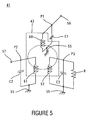
- Fig. 5 is an equivalent circuit of the lumped-constant isolator 41.
- the lumped-constant isolator 41 includes a rectangular permanent magnet 42, a central electrode assembly 43, a mounting multilayer ceramic substrate 44, an upper side casing 45, and a lower side casing 46, the latter two casings each being used as a metal casing.
- the upper side casing 45 has a box shape having an opening facing downward and is formed of an upper wall portion 47 and four side wall portions 48 to 51.
- the lower side casing 46 includes two standing walls 52 and 53 facing each other and a bottom wall portion 54 connecting between the standing walls 52 and 53.
- the upper side casing 45 and the lower side casing 46 are each formed of a ferromagnetic material, and the surfaces thereof are processed by Ag or Cu plating.
- the multilayer ceramic substrate 44 has a multilayer structure which includes ceramic layers laminated to each other and which incorporates matching capacitor elements C1, C2, and C3 and a resistor element R as shown in Fig. 5 .
- the built-in structures of the matching capacitor elements C1 to C3 and the resistor element R are substantially the same as those of the built-in capacitor 33 and the thick film resistor 35 in the multilayer ceramic substrate 21 shown in Fig. 3 .
- trimming tracks of these passive elements remain in the multilayer ceramic substrate 44.
- port electrodes P1, P2, and P3 and earth electrodes 55 are exposed on the upper surface of the multilayer ceramic substrate 44.
- an input electrode 56 and an output electrode 57 electrically connecting this isolator 41 to an external circuit are formed on the lower surface of the multilayer ceramic substrate 44.
- the central electrode assembly 43 has a rectangular base 58 formed of microwave ferrite. On an upper surface 59 of the base 58, 3 central electrodes 60, 61, and 62 are disposed. These central electrodes 60 to 62 are insulated from each other by electrical insulating layers 63 provided therebetween. In addition, the three central electrodes 60 to 62 are disposed so as to cross each other with an angle of approximately 120°.
- the central electrode 62, the electrical insulating layer 63, the central electrode 61, the electrical insulating layer 63, and the central electrode 60 are disposed in that order from the bottom.
- One-side ends of these central electrodes 60 to 62 are connected to an earth electrode 67 formed on a lower surface 66 of the base 58 through connection electrodes 65 formed on side surfaces 64 of the base 58, and the other-side ends of these central electrodes 60 to 62 are connected to the port electrodes P1 to P3 of the multilayer ceramic substrate 44 through the connection electrodes 65 formed on the side surfaces 64.
- the earth sides of the central electrodes 60 to 62 are connected to the common earth electrode 67 through the connection electrodes 65.
- This common earth electrode 67 has a shape approximately the same as that of the lower surface 66 of the base 58 and covers almost an entire surface of the lower surface 66 so as not to be in contact with the port electrodes P1 to P3 formed on the multilayer ceramic substrate 44.
- the earth electrode 67 is connected to the earth electrodes 55 on the multilayer ceramic substrate 44.
- the multilayer ceramic substrate 44 is set in the lower side casing 46, and the central electrode assembly 43 is placed on the multilayer ceramic substrate 44, so that a predetermined electrical connection is performed.
- the permanent magnet 42 is disposed at the lower surface side of the upper wall portion 47 of the upper side casing 45. Subsequently, while the state thus formed is maintained, the upper side casing 45 and the lower side casing 46 are connected to each other, so that a united metal casing is formed.
- the permanent magnet 42 applies a direct current magnetic field to the central electrode assembly 43.
- the metal casing composed of the upper side casing 45 and the lower side casing 46 forms a magnetic circuit and also functions as a yoke.
- the multilayer ceramic substrate and the method for manufacturing the same may be applied to a nonreciprocal circuit device and a method for manufacturing the same, the nonreciprocal circuit device including a permanent magnet; a central electrode assembly which has a base, a plurality of central electrodes disposed on the base to cross each other with a predetermined crossing angle, and electrical insulating layers disposed between the central electrodes to electrically insulate therebetween, and which is applied with a direct current magnetic field by the permanent magnet; a casing accommodating the permanent magnet and the central electrode assembly; and a multilayer ceramic substrate mounting the central electrode assembly and provided with a capacitor element and a resistor element.
- the multilayer ceramic substrate and the method for manufacturing the same, according to the present invention may also be applied, besides a nonreciprocal circuit device and a method for manufacturing the same, to various module ceramic substrates and a method for manufacturing the same.
- the capacitance regulation by laser trimming is not limited to milling of part of the first capacitor electrode, that is, is not limited to capacitance regulation by decreasing an electrode area, and for example, the capacitance regulation may be performed by dividing one first capacitor electrode into at least two parts.
- trimming of the second capacitor electrode may be simultaneously performed when laser trimming is performed for the first capacitor electrode.
- BaCO 3 , TiO 2 , Nd 2 O 3 , and Sm 2 O 3 powders were mixed together at a ratio, on a molar percent basis, of 13%, 58%, 10%, and 19%, respectively.
- the sintered bodies thus obtained were each processed by using YAG laser to irradiate the first capacitor electrode with laser light at an output of 2 kHz with a scan number of 7 (conditions of laser trimming), so that the first capacitor electrode was trimmed to decrease the capacitor's capacitance from 20 pF at the beginning to 10 pF.
- the insulation resistances (logIR) before and after the trimming were respectively measured, and by an LCR meter, the Q values at 1 MHz before and after the trimming were also respectively measured.
- the relative dielectric constant ⁇ r of the dielectric glass ceramic layer after the trimming was measured by an LCR meter, and the flexural strength (MPa) of the dielectric glass ceramic layer after the trimming was also measured.
- Fig. 6 is a graph showing the rates of change in insulation resistance and Q value with respect to the content (volume percent) of the BaO-Re 2 O 3 -4TiO 2 -based ceramic. Table 1 SAMPLE NO.
- GLASS CERAMIC COMPOSITION INSULATION RESISTANCE (logIR) Q VALUE at 1 MHz JUDGMENT OF TRIMMING PERFORMA NCE RELATIVE DIELECTRIC CONSTANT ⁇ r FLEXURAL STRENGTH (MPa) BRT (VOLUME PERCENT) Al 2 O 3 VOLUME PERCENT) GLASS (VOLUME PERCENT) BEFORE TRIMMING AFTER TRIMMING RATE OF CHANGE (%) BEFORE TRIMMING AFTER TRIMMING RATE OF CHANGE (%) 1 5.0 32.0 63.0 13.13 12.81 102.5 1236 1251 98.8 G 8.5 312 2 10.0 5.0 85.0 12.78 12.91 99.0 1324 1319 100.4 G 8.1 283 3 10.0 11.0 79.0 13.45 11.83 113.7 1351 1326 101.9 G 10.4 293 4 10.0 24.9 65.1 12.86 12.99 99.0 1398 1371 102.0 G 11.6 301
Landscapes
- Engineering & Computer Science (AREA)
- Power Engineering (AREA)
- Microelectronics & Electronic Packaging (AREA)
- Chemical & Material Sciences (AREA)
- Manufacturing & Machinery (AREA)
- Ceramic Engineering (AREA)
- Inorganic Chemistry (AREA)
- Fixed Capacitors And Capacitor Manufacturing Machines (AREA)
- Ceramic Capacitors (AREA)
- Production Of Multi-Layered Print Wiring Board (AREA)
Abstract


Description
- The present invention relates to a method for regulating the capacitance value of a capacitor to be built in a multilayer ceramic substrate, and a multilayer ceramic substrate and a method for manufacturing the same, and more particularly relates to a method for regulating the capacitance value of a built-in capacitor by laser trimming.
- In recent years, in information processing apparatuses represented, for example, by a mobile communication terminal and a personal computer, an increase in information processing speed, miniaturization of an apparatus, enhancement of multifunctionality, and the like have been actively pursued, and the improvement in performances of the information processing apparatuses as described above has been realized primarily by an increase in integration, an increase in processing speed, and enhancement of functionality of semiconductor devices, such as VLSI and ULSI.
- However, even though the increase in processing speed and enhancement of functionality of semiconductor devices have been accomplished, signal delay, crosstalk, impedance mismatch, noise generation caused by fluctuation of power source output, and the like may occur on a substrate on which devices are connected to each other, and as a result, the system performance may be limited in some cases.
- Accordingly, as an electronic component used in a high speed and high performance information processing apparatus, a so-called multichip module (MCM: Multi-Chip Module) in which a plurality of semiconductor devices is mounted on a ceramic substrate has been practically used. As a substrate for the module as described above, a multilayer ceramic substrate on which a wiring pattern for electrically connecting semiconductor devices in a three-dimensional manner is provided is effectively used, and as a material for this type of multilayer ceramic substrate, alumina has been used.
- In a multilayer ceramic substrate using alumina, since a sintering temperature of an alumina powder is high, such as 1,500°C or more, as a material for an inner layer wiring pattern, a high melting point metal, such as tungsten or molybdenum, must be used. However, since the high melting point metals as described above have a high specific resistance, the loss of signal increases, particularly in a high frequency region.
- In order to solve the above problem, a multilayer ceramic substrate has been developed which is formed by laminating a plurality of glass ceramic green sheets, followed by sintering. Since the glass ceramic green sheets are formed by adding a vehicle containing a binder, a solvent, and the like to a ceramic powder and a glass powder, followed by mixing, and the sintering temperature is 1,050°C or less, simultaneous firing can be performed with a low temperature melting point metal, such as silver or copper, having a low specific resistance, and a multilayer ceramic substrate having a small signal loss in a high frequency region and superior electrical properties can be obtained.
- In addition, in recent years, an attempt has been made in which a passive element, such as a capacitor, mounted on a multilayer ceramic substrate as a surface mounting element is built in a multilayer ceramic substrate so that an entire module is further miniaturized.
- In the case in which the element as described above is built in a multilayer ceramic substrate, when electrical properties of the element is degraded as compared to that of a surface mounting element mounted on a substrate surface, the merit obtained by a built-in element is reduced by approximately half; hence, it is required that a built-in element have properties equal to or more than those of an element mounted on a substrate. Hence, as a substrate material which is used as a base, in general, a material is selected so that sufficient electrical properties of each built-in element can be obtained.
- For example, in Japanese Unexamined Patent Application Publications Nos.
9-92983 2000-58381 - Incidentally, the capacitance value of a capacitor built in a multilayer ceramic substrate may vary lot by lot in some cases because of, for example, the variation in thickness of ceramic green sheets, the variation in printed area of capacitor electrodes, the variation generated when ceramic green sheets are laminated to each other, and the variation in shrinkage which occurs when ceramic green sheets are fired. Accordingly, in order to achieve a highly precise capacitance value of a built-in capacitor, it is necessary to perform trimming of a capacitor electrode with laser or the like. That is, it is necessary that by milling the area of a capacitor electrode using laser trimming, the capacitance value of a built-in capacitor be set to a desired value.
- However, when laser trimming is performed, a dielectric ceramic layer provided between capacitor electrodes is partly milled besides the capacitor electrode, and as a result, after the trimming is performed, the insulation resistance between the capacitor electrodes may decrease and/or the Q value of the capacitor may decrease in some cases.
- Patent Document 1: Japanese Unexamined Patent Application Publication No.
9-92983 - Patent Document 2: Japanese Unexamined Patent Application Publication No.
2000-58381 - The present invention has been conceived in consideration of the above-described situation, and an object of the present invention is to provide a method for regulating the capacitance value of a built-in capacitor, which can precisely regulate the capacitance value of a built-in capacitor without significantly changing the insulation resistance and Q value before and after laser trimming.
- Another object of the present invention is to provide a multilayer ceramic substrate obtained by using the above method for regulating the capacitance value of a built-in capacitor.
- Still another object of the present invention is to provide a method for manufacturing a multilayer ceramic substrate, which is performed by using the above method for regulating the capacitance value of a built-in capacitor. Means for Solving the Problems
- The present invention is first directed to a method for regulating the capacitance value of a built-in capacitor of a multilayer ceramic substrate which includes: a ceramic laminate having a plurality of ceramic layers laminated to each other; and a first and a second capacitor electrode disposed to face each other with a specific one of the ceramic layers interposed therebetween so as to form the built-in capacitor.
- The method for regulating the capacitance value of a built-in capacitor, according to the present invention, includes the step of performing laser trimming of the first capacitor electrode, and the specific ceramic layer disposed between the first and the second electrodes is a TiO2-based dielectric glass ceramic layer which contains 10 to 35 percent by volume of dielectric grains including TiO2.
- In the method for regulating the capacitance value of a built-in capacitor, according to the present invention, the TiO2-based dielectric glass ceramic layer preferably has a layer thickness of 12.5 to 50 µm.
- The first and the second capacitor electrodes may both be built in the ceramic laminate.
- The TiO2-based dielectric glass ceramic layer preferably includes:
- (A) 10 to 35 percent by volume of a BaO-TiO2-ReO3/2-based ceramic represented by xBaO-yTiO2-zReO3/2 (where x, y, and z each indicate molar percent; 8≤x≤18, 52.5≤y≤65, and 20≤z≤40 hold; x+y+z=100 holds; and Re indicates a rare earth element);
- (B) 5 to 42 percent by volume of an alumina ceramic; and
- (C) 50 to 79 percent by volume of a borosilicate glass which includes 4 to 17.5 percent by weight of B2O3, 28 to 50 percent by weight of SiO2, 0 to 20 percent by weight of Al2O3, and 36 to 50 percent by weight of MO (where MO is at least one selected from the group consisting of CaO, MgO, SrO, and BaO), and in addition,
- In the above glass ceramic composition, the borosilicate glass may further include less than 0.5 percent by weight of at least one selected from the group consisting of Li2O, Na2O, and K2O.
- In addition, the present invention is also directed to a method for manufacturing a multilayer ceramic substrate, including the steps of: forming a multilayer ceramic substrate before being processed by trimming, which includes a ceramic laminate having a plurality of ceramic layers laminated to each other, and a first and a second capacitor electrode disposed to face each other with a specific one of the ceramic layers interposed therebetween so as to form a built-in capacitor; and performing laser trimming of the first capacitor electrode in order to regulate the capacitance value of the built-in capacitor.
- According to the method for manufacturing a multilayer ceramic substrate of the present invention, in the step of forming a multilayer ceramic substrate before being processed by trimming, the specific ceramic layer located between the first and the second capacitor electrodes may be formed of a TiO2-based dielectric glass ceramic layer in which the content of dielectric grains including TiO2 is 10 to 35 percent by volume.
- Furthermore, the present invention is also directed to a multilayer ceramic substrate including: a ceramic laminate having a plurality of ceramic layers laminated to each other; and a first and a second capacitor electrode disposed to face each other with a specific one of the ceramic layers interposed therebetween so as to form a built-in capacitor.
- In the multilayer ceramic substrate according to the present invention, the specific ceramic layer located between the first and the second capacitor electrodes may be a TiO2-based dielectric glass ceramic layer in which the content of dielectric grains including TiO2 is 10 to 35 percent by volume, and the first capacitor electrode may have a trimming track formed when the built-in capacitor is processed by laser trimming.
- According to the method for regulating the capacitance value of a built-in capacitor of the present invention, when the first capacitor electrode is processed by laser trimming in order to regulate the capacitance value of a built-in capacitor, since the ceramic layer provided between the first and the second capacitor electrodes is a TiO2-based dielectric glass ceramic layer in which the content of the dielectric grains (hereinafter referred to as "TiO2-based dielectric grains" in some cases) including TiO2 is 10 to 35 percent by volume, the insulation resistance between the capacitor electrodes and the Q value of the capacitor are not significantly changed before and after the laser trimming, and the capacitance value of the built-in capacitor can be precisely regulated.
- That is, the changes in insulation resistance and Q value are induced by the change in properties, which is caused by the laser trimming, of the dielectric glass ceramic layer between the capacitor electrodes and are particularly induced by semiconductorization of the TiO2-based dielectric grains of the dielectric glass ceramic layer. Hence, by specifying the ratio (volume ratio) of the TiO2-based grains which are responsible for the change in properties, without substantially degrading the insulation resistance and the Q value, the capacitance value of the built-in capacitor can be precisely regulated.
- In addition, according to the method for manufacturing a multilayer ceramic substrate of the present invention, when the method for regulating the capacitance value of a built-in capacitor, according to the present invention, is used, a multilayer ceramic substrate which includes a built-in capacitor having superior insulation resistance and Q value can be manufactured with good reproducibility.
- In addition, the multilayer ceramic substrate according to the present invention is obtained by using the method for regulating the capacitance value of a built-in capacitor of the present invention. Hence, according to the multilayer ceramic substrate of the present invention, in the built-in capacitor provided therein, the capacitance value is precisely regulated, and further, the insulation reliability and the Q value can also be made excellent.
-
-
Fig. 1 includes cross-sectional views each schematically showing part of a multilayerceramic substrate 1 for illustrating a method for regulating the capacitance value of a built-in capacitor according to the present invention. -
Fig. 2 is a view corresponding to that shown inFig. 1 for illustrating a comparative example of the method for regulating the capacitance value of a built-in capacitor according to the present invention. -
Fig. 3 is a cross-sectional view schematically showing a multilayerceramic substrate 21 of one embodiment according to the present invention. -
Fig. 4 is an exploded perspective view of a lumped-constant isolator 41 as one example of a nonreciprocal circuit device having a multilayerceramic substrate 44 according to another embodiment of the present invention. -
Fig. 5 is an equivalent circuit of the lumped-constant isolator 41 shown inFig. 4 . -
Fig. 6 is a graph showing the rate of change in insulation resistance and the rate of change in Q value with respect to the content (volume percent) of a BaO-Re2O3-4TiO2-based dielectric glass ceramic. -
- 1,
- 21, 44 multilayer ceramic substrate
- 2,
- 33 built-in capacitor
- 3
- to 5, 22, 23 ceramic layer
- 6,
- 24 ceramic laminate
- 7,
- 26 first capacitor electrode
- 8,
- 27 second capacitor electrode
- 9
- TiO2-based dielectric grain
- 10
- laser light
- 11, 34
- trimming track
- First, with reference to
Fig. 1 , a method for regulating the capacitance value of a built-in capacitor, according to the present invention, will be described in detail. InFig. 1 , schematic cross-sectional views are shown each indicating part of a multilayerceramic substrate 1 in which a built-incapacitor 2 is formed. - As shown in
Fig. 1(A) , the multilayerceramic substrate 1 has aceramic laminate 6 formed ofceramic layers ceramic laminate 6, the built-incapacitor 2 is formed. The built-incapacitor 2 is formed of afirst capacitor electrode 7, asecond capacitor electrode 8 disposed to face thefirst capacitor electrode 7, and theceramic layer 4 provided between the first and thesecond capacitor electrodes ceramic layer 4 is a dielectric glass ceramic layer and is a dielectric layer including TiO2-baseddielectric grains 9, and the ratio of the TiO2-basedgrains 9 is set to 10 to 35 percent by volume. - The capacitance value of the
capacitor 2 built in the multilayerceramic substrate 1 may vary lot by lot in some cases because of, for example, the variation in thickness of a ceramic green layer to be formed into theglass ceramic layer 4, the variation in screen printed area of conductor patterns to be formed into the first and thesecond capacitor electrodes capacitor 2 to a desired value, as shown inFig. 1(B) , by using YAG (Yttrium Aluminum Garnet) laser or the like,laser light 10 is irradiated to thefirst capacitor electrode 7 in theceramic laminate 6 provided in the multilayerceramic substrate 1. - Accordingly, as shown in
Fig. 1(C) , by thelaser light 10 thus irradiated, thefirst capacitor electrode 7 is milled together with theceramic layer 3, and a processed hole (trimming track) 11 is formed. As a result, part of thefirst capacitor electrode 7 is milled, and in addition, in this step, the processedhole 11 reaches part of the dielectricglass ceramic layer 4; hence, the dielectricglass ceramic layer 4 is also partly milled. - In this embodiment, the dielectric
glass ceramic layer 4 having a high dielectric constant is formed, for example, of a titanium oxide-based material, such as barium titanate, calcium titanate, or strontium titanate, and in the above materials, a titanium oxide-based crystalline phase (TiO2-based dielectric grains), such as a BaTiO3 crystalline phase, a CaTiO3 crystalline phase, or a SrTiO3 crystalline phase, is a primary crystalline phase. In addition, since heat generated by the irradiation of thelaser light 10 instantaneously reaches 2,000°C, when this heat is applied to the TiO2-baseddielectric grains 9 in the dielectricglass ceramic layer 4, tetravalent titanium forming the TiO2-baseddielectric grains 9 is reduced to trivalent titanium (Ti4+ → Ti3+). - As a result, oxygen holes are formed in the
dielectric grains 9, and thedielectric grains 9 are semiconductorized. That is, by the laser trimming, part of the TiO2-baseddielectric grains 9, which is in the vicinity of the place irradiated with thelaser light 10, is changed to semiconductorized TiO2-baseddielectric grains 9a. - As for the above semiconductorization, according to the present invention, since the ratio of the TiO2-based
dielectric grains 9 in the TiO2-based dielectricglass ceramic layer 4 is low, such as 10 to 35 percent by volume, even when the TiO2-baseddielectric grains 9 are semiconductorized, the semiconductorizeddielectric grains 9a are not connected to each other between thefirst capacitor electrode 7 and thesecond capacitor electrode 8 as shown inFig. 1(C) ; hence, even after the laser trimming, the insulation resistance and the Q value hardly decrease. -
Fig. 2 is a view for illustrating a comparative example of the method for regulating a built-in capacitor according to the present invention, the view being corresponding toFig. 1 . InFig. 2 , elements corresponding to those shown inFig. 1 are designated by reference numerals similar to those described above, and duplicated description is omitted. - In the case in which the ratio of the TiO2-based
dielectric grains 9 in the TiO2-based dielectricglass ceramic layer 4 is more than 35 percent by volume, since the ratio of the TiO2-baseddielectric grains 9 becomes excessively large, when thedielectric grains 9 are semiconductorized, as shown inFig. 2 , the semiconductorizeddielectric grains 9a are connected to each other between thefirst capacitor electrode 7 and thesecond capacitor electrode 8. - As a result, by the laser trimming, the
first capacitor electrode 7 and thesecond capacitor electrode 8 are shortcircuited therebetween, and hence the insulation resistance is significantly decreased. In addition, when the insulation properties of the dielectricglass ceramic layer 4 are degraded, loss of Joule heat occurs thereby, and the Q value of the capacitor decreases. The semiconductorizeddielectric grains 9a can be returned to the original state by performing a re-oxidation treatment; however, in this case, the re-oxidation treatment is necessarily performed as an additional treatment, and in addition, by the re-oxidation treatment, the insulation resistance and the Q value of the built-incapacitor 2 are again changed, so that the variation may occur in some cases. - As described above, according to the present invention, in the TiO2-based dielectric
glass ceramic layer 4, since the ratio of the TiO2-baseddielectric grains 9 is 10 to 35 percent by volume, the insulation resistance between thecapacitor electrodes capacitor 2 are not significantly changed before and after the laser trimming, and in addition, without performing an additional treatment, such as a re-oxidation treatment, the capacitance value of the built-incapacitor 2 can be precisely regulated. - In addition, the relative dielectric constant of the TiO2-based dielectric
glass ceramic layer 4 primarily depends on the volume ratio of the TiO2-baseddielectric grains 9 present therein, and when the ratio of the TiO2-baseddielectric grains 9 is less than 10 percent by volume, as the dielectricglass ceramic layer 4 forming the built-incapacitor 2, a sufficient relative dielectric constant εr cannot be obtained. By the reasons as described above, the volume ratio of the TiO2-baseddielectric grains 9 is required to be in the range of 10% to 35%, and in addition, in this range, a volume ratio of 20% to 35% is particularly preferable. In addition, the grain diameter (D50) of the TiO2-baseddielectric grains 9 is preferably in the range of 0.9 to 2.5 µm and is more preferably in the range of 1.0 to 1.5 µm. - In addition, the layer thickness (element thickness) of the TiO2-based dielectric
glass ceramic layer 4 is preferably in the range of 12.5 to 50 µm. When the layer thickness is less than 12.5 µm, even when the occupation ratio of the TiO2-baseddielectric grains 9 is set as described above, the insulation resistance and/or the Q value may be changed in some cases before and after the laser trimming. In addition, when the layer thickness is more than 50 µm, since the distance between thecapacitor electrodes capacitor 2. - As for the positions of the first and the
second capacitor electrodes ceramic laminate 6 as shown inFig. 1 . When thefirst capacitor electrode 7 to be processed by trimming is formed inside theceramic laminate 6, compared to the case in which thefirst capacitor electrode 7 is disposed on the surface of theceramic laminate 6,laser light 10 having a large power must be irradiated; however, even if thelaser light 10 having a large power is used, when the occupation ratio of the TiO2-baseddielectric grains 9 in the TiO2-based dielectricglass ceramic layer 4 is specified as described above, without significantly changing the insulation resistance and the Q value, the capacitance value of the built-incapacitor 2 can be precisely regulated. - In the multilayer
ceramic substrate 1 described above, theceramic layers glass ceramic layer 4; however, another ceramic material having a low relative dielectric constant, such as a low-temperature sinterable ceramic (LTCC, Low Temperature Co-fired Ceramic) material, is preferably used. The low-temperature sinterable ceramic material is a ceramic material which can be sintered at a temperature of 1,050°C or less and which can be co-fired with silver, copper, or the like having a low specific resistance. As the low-temperature sinterable ceramic material, in particular, for example, there may be mentioned a glass composite-based LTCC material formed by mixing a borosilicate glass with a powdered ceramic, such as alumina, zirconia, magnesia, or forsterite; a crystalline glass-based LTCC material using a ZnO-MgO-Al2O3-SiO2-based crystalline glass; and a non-glass-based LTCC material such as a BaO-Al2O3-SiO2-based powder ceramic or an Al2O3-CaO-SiO2-MgO-B2O3-based powder ceramic. - The TiO2-based dielectric
glass ceramic layer 4 preferably includes: - (A) 10 to 35 percent by volume of a BaO-TiO2-ReO3/2-based ceramic represented by xBaO-yTiO2-zReO3/2 (where x, y, and z each indicate molar percent; 8≤x≤18, 52.5≤y≤65, and 20≤z≤40 hold; x+y+z=100 holds; and Re indicates a rare earth element);
- (B) 5 to 42 percent by volume of an alumina ceramic; and
- (C) 50 to 79 percent by volume of a borosilicate glass which includes 4 to 17.5 percent by weight of B2O3, 28 to 50 percent by weight of SiO2, 0 to 20 percent by weight of Al2O3, and 36 to 50 percent by weight of MO (where MO is at least one selected from the group consisting of CaO, MgO, SrO, and BaO), and
- From the glass ceramic composition as described above, a sintered body can be formed to have a relatively high relative dielectric constant, and in addition, when a ceramic substrate incorporating a resistance element therein is formed, the resistance properties of the resistance element are not degraded.
- In the above glass ceramic composition, the BaO-TiO2-ReO3/2-based ceramic represented by xBaO-yTiO2-zReO3/2 is formed into the TiO2-based
dielectric grains 9 by firing. In this glass ceramic composition, when the ratio of the alumina ceramic is less than 5 percent by volume, the flexural strength of the multilayerceramic substrate 1 after firing tends to decrease, and on the other hand, when the above ratio is more than 42 percent by volume, since the ratio of the BaO-TiO2-ReO3/2-based ceramic decreases, a relative dielectric constant necessary as the built-incapacitor 2 may not be obtained in some cases. - In addition, when the ratio of the borosilicate glass is less than 50 percent by volume, the sintering properties of the multilayer
ceramic substrate 1 may be insufficient in some cases, and on the other hand, when the above ratio is more than 79 percent by volume, since the ratio of the BaO-TiO2-ReO3/2-based ceramic relatively decreases, a relative dielectric constant necessary as the built-incapacitor 2 may not be obtained in some cases. - In addition, when the total amount of the BaO-TiO2-ReO3/2-based ceramic and the alumina ceramic is less than 21 percent by volume, since the ratio of the BaO-TiO2-ReO3/2-based ceramic relatively decreases, a relative dielectric constant necessary as the built-in
capacitor 2 may not be obtained in some cases, and in addition, the flexural strength also tends to decrease. - In addition, although being described in detail in PCT International Publication No.
W02006/046361 Pamphlet by the inventors of the present invention, in the BaO-TiO2-ReO3/2-based ceramic represented by xBaO-yTiO2-zReO3/2, when x is less than 8, the relative dielectric constant and the Q values decrease, and in addition, the absolute value of a temperature coefficient of capacitance (TCC) of the relative dielectric constant may increase in some cases. On the other hand, when x is more than 18, the Q value decreases, and in addition, the absolute value of TCC also tends to increase. In addition, when y is less than 52.5, the relative dielectric constant may decrease in some cases, and on the other hand, when y is more than 65, the absolute value of TCC tends to increase. In addition, when z is less than 20, the absolute value of TCC may increase in some cases; on the other hand, when z is more than 40, the absolute value of TCC increases, and in addition, the relative dielectric constant also tends to decrease. In addition, as Re (rare earth element), Nd, Pr, Sm, or the like may be used. - In the borosilicate glass, when the content of B2O3 is less than 4 percent by weight, the sintering properties may become insufficient in some cases, and on the other hand, when the content is more than 17.5 percent by weight, since the humidity resistance degrades, PCT (Pressure Cooker Test) reliability degrades, and dielectric breakdown may occur. In addition, when the content of SiO2 is less than 28 percent by weight, since the humidity resistance degrades as is the case described above, the PCT reliability degrades, and dielectric breakdown may occur. On the other hand, when the content of SiO2 is more than 50 percent by weight, the sintering properties tend to be insufficient.
- In addition, in the borosilicate glass, Al2O3 may not be contained; however, Al2O3 is preferably contained since the humidity resistance is improved. However, when the content of Al2O3 is more than 20 percent by weight, the Q value tends to decrease.
- In addition, in the borosilicate glass, when the content of MO is less than 36 percent by weight, the sintering properties may be insufficient in some cases, and on the other hand, when the content is more than 50 percent by weight, since the humidity resistance degrades, the PCT reliability degrades, and hence dielectric breakdown may occur. Although at least one selected from the group consisting of CaO, MgO, SrO, and BaO may be used as MO, in order to obtain a high Q value of the dielectric
glass ceramic layer 4, in particular, CaO is preferably used. - In addition, the borosilicate glass preferably further contains at least one selected from the group consisting of Li2O, Na2O, and K2O in an amount of less than 0.5 percent by weight. When at least one of these alkali metal oxides is contained in the range described above, a high relative dielectric constant can be obtained. When the content of the alkali metal oxide is more than 0.5 percent by weight, the humidity resistance tends to degrade.
- The above glass ceramic composition may further contain 20 percent by weight or less of CaTiO3. When CaTiO3 in the range described above is contained, a high relative dielectric constant can be obtained. In addition, when the content of CaTiO3 is more than 20 percent by weight, the absolute value of TCC tends to increase.
- In addition, the glass ceramic composition may further contain 3 parts by weight or less of CeO2 with respect to 100 parts by weight of the total of the BaO-TiO2-ReO3/2-based ceramic, the alumina ceramic, and the borosilicate glass. When CeO2 is contained in the range described above, and Ag is used as an electrode material, discoloration of part of a substrate in the vicinity of the electrode, which is caused by colloid formation of Ag used as an electrode material, can be suppressed. In addition, when the content of Ce2O is more than 3 percent by weight, the Q value of the dielectric glass ceramic layer tends to decrease.
- In addition, when at least one of TiO2 and ZrO2 in an amount of 1 percent by weight or less is added to the glass ceramic composition, the absolute value of the rate of change in temperature of relative dielectric constant of a sintered body can be decreased which is obtained by sintering the above composition. Since this TiO2 is to be contained in the TiO2-based
dielectric grains 9 of the TiO2-based dielectricglass ceramic layer 4 after the firing, in consideration of the ratio of the grains formed of this TiO2, the amount of the TiO2-baseddielectric grains 9 must be adjusted within the range described above. - Next, a concrete structure of the multilayer ceramic substrate according to the present invention and a method for manufacturing the same will be described.
- As shown in
Fig. 3 , a multilayerceramic substrate 21 has aceramic laminate 24 formed ofceramic layers 22 andceramic layers 23 laminated to each other. Theceramic layers 22 are each a ceramic layer formed of the low-temperature sinterable ceramic material described above, and theceramic layers 23 are each the TiO2-based dielectric glass ceramic layer described above. - Relating to the
ceramic layers external conductors 25 formed on the external surface of the multilayerceramic substrate 21,several interlayer conductors 26 to 31 formed along interfaces between theceramic layers hole conductors 32 provided to penetrate specific layers of theceramic layers - Among the
conductive patterns 25 to 32, besides patterns provided simply as wires, there are patterns provided to form at least one passive element, such as a capacitor and/or an inductor, inside the multilayerceramic substrate 21. For example, theinterlayer conductors 26 to 30 are to be formed into capacitor electrodes. From thecapacitor electrodes 26 to 30 and theceramic layers 23 disposed therebetween, a built-incapacitor 33 is formed. From the structure described above, it is understood that a built-in capacitor may be formed from at least three capacitor electrodes as well as from two capacitor electrodes. At least one of thecapacitor electrodes 26 to 30 may also be used as a ground electrode. - In this multilayer
ceramic substrate 21, a trimmingtrack 34 remains which is formed by the above method for regulating the capacitance value of the above built-incapacitor 33. This trimmingtrack 34 is formed by performing laser trimming of thecapacitor electrode 26 from one primary surface side of the multilayerceramic substrate 21 obtained by a general sheet lamination method or a thick film printing lamination method. In addition, the trimmingtrack 34 may be filled with a glass or a resin in order to prevent the variation in capacitance which may occur after the capacitance regulation is performed. - In addition, a
thick film resistor 35 is built in the multilayerceramic substrate 21. Thethick film resistor 35 is formed of a resistor film provided along the interface between theceramic layers thick film resistor 35 is processed by laser trimming to regulate the resistor value thereof, even if theceramic layer 23 is partly milled, since theceramic layer 23 is formed of the TiO2-based dielectric glass ceramic layer described above, the change in properties before and after the trimming is small. - Next, one example of an electronic component formed by using the multilayer ceramic substrate according to the present invention will be described with reference to
Figs. 4 and5 .Fig. 4 is an exploded perspective view showing a lumped-constant isolator 41 as one example of a nonreciprocal circuit device, andFig. 5 is an equivalent circuit of the lumped-constant isolator 41. - As shown in
Fig. 4 , the lumped-constant isolator 41 includes a rectangularpermanent magnet 42, acentral electrode assembly 43, a mounting multilayerceramic substrate 44, anupper side casing 45, and alower side casing 46, the latter two casings each being used as a metal casing. - The
upper side casing 45 has a box shape having an opening facing downward and is formed of anupper wall portion 47 and fourside wall portions 48 to 51. Thelower side casing 46 includes two standingwalls bottom wall portion 54 connecting between the standingwalls upper side casing 45 and thelower side casing 46 are each formed of a ferromagnetic material, and the surfaces thereof are processed by Ag or Cu plating. - Hereinafter, with reference to
Fig. 5 together withFig. 4 , thecentral electrode assembly 43 and the multilayerceramic substrate 44 will be described in detail. - Although a mechanical structure of the multilayer
ceramic substrate 44 is not shown in the figures, the multilayerceramic substrate 44 has a multilayer structure which includes ceramic layers laminated to each other and which incorporates matching capacitor elements C1, C2, and C3 and a resistor element R as shown inFig. 5 . The built-in structures of the matching capacitor elements C1 to C3 and the resistor element R are substantially the same as those of the built-incapacitor 33 and thethick film resistor 35 in the multilayerceramic substrate 21 shown inFig. 3 . In addition, although being not shown in the figure, trimming tracks of these passive elements remain in the multilayerceramic substrate 44. - On the upper surface of the multilayer
ceramic substrate 44, port electrodes P1, P2, and P3 andearth electrodes 55 are exposed. Although not being shown inFig. 4 , on the lower surface of the multilayerceramic substrate 44, aninput electrode 56 and anoutput electrode 57 electrically connecting thisisolator 41 to an external circuit are formed. - The
central electrode assembly 43 has arectangular base 58 formed of microwave ferrite. On an upper surface 59 of thebase central electrodes central electrodes 60 to 62 are insulated from each other by electrical insulatinglayers 63 provided therebetween. In addition, the threecentral electrodes 60 to 62 are disposed so as to cross each other with an angle of approximately 120°. - Although the order of placement of the
central electrodes 60 to 62 may be arbitrarily determined, in the embodiment shown inFig. 4 , thecentral electrode 62, the electrical insulatinglayer 63, thecentral electrode 61, the electrical insulatinglayer 63, and thecentral electrode 60 are disposed in that order from the bottom. One-side ends of thesecentral electrodes 60 to 62 are connected to anearth electrode 67 formed on alower surface 66 of the base 58 throughconnection electrodes 65 formed onside surfaces 64 of thebase 58, and the other-side ends of thesecentral electrodes 60 to 62 are connected to the port electrodes P1 to P3 of the multilayerceramic substrate 44 through theconnection electrodes 65 formed on the side surfaces 64. - As described above, the earth sides of the
central electrodes 60 to 62 are connected to thecommon earth electrode 67 through theconnection electrodes 65. Thiscommon earth electrode 67 has a shape approximately the same as that of thelower surface 66 of thebase 58 and covers almost an entire surface of thelower surface 66 so as not to be in contact with the port electrodes P1 to P3 formed on the multilayerceramic substrate 44. In addition, theearth electrode 67 is connected to theearth electrodes 55 on the multilayerceramic substrate 44. - When the lumped-
constant isolator 41 is formed by using the constituent elements described above, first, the multilayerceramic substrate 44 is set in thelower side casing 46, and thecentral electrode assembly 43 is placed on the multilayerceramic substrate 44, so that a predetermined electrical connection is performed. In addition, thepermanent magnet 42 is disposed at the lower surface side of theupper wall portion 47 of theupper side casing 45. Subsequently, while the state thus formed is maintained, theupper side casing 45 and thelower side casing 46 are connected to each other, so that a united metal casing is formed. - When the constituent elements are assembled as described above, the
permanent magnet 42 applies a direct current magnetic field to thecentral electrode assembly 43. In this case, the metal casing composed of theupper side casing 45 and thelower side casing 46 forms a magnetic circuit and also functions as a yoke. - As described above, the multilayer ceramic substrate and the method for manufacturing the same, according to the present invention, may be applied to a nonreciprocal circuit device and a method for manufacturing the same, the nonreciprocal circuit device including a permanent magnet; a central electrode assembly which has a base, a plurality of central electrodes disposed on the base to cross each other with a predetermined crossing angle, and electrical insulating layers disposed between the central electrodes to electrically insulate therebetween, and which is applied with a direct current magnetic field by the permanent magnet; a casing accommodating the permanent magnet and the central electrode assembly; and a multilayer ceramic substrate mounting the central electrode assembly and provided with a capacitor element and a resistor element.
- The multilayer ceramic substrate and the method for manufacturing the same, according to the present invention, may also be applied, besides a nonreciprocal circuit device and a method for manufacturing the same, to various module ceramic substrates and a method for manufacturing the same.
- In addition, in the present invention, the capacitance regulation by laser trimming is not limited to milling of part of the first capacitor electrode, that is, is not limited to capacitance regulation by decreasing an electrode area, and for example, the capacitance regulation may be performed by dividing one first capacitor electrode into at least two parts. In addition, trimming of the second capacitor electrode may be simultaneously performed when laser trimming is performed for the first capacitor electrode.
- Next, the present invention will be described in detail with reference to concrete experimental examples. However, the present invention is not limited to the following experimental examples.
- First, in order to form a powdered BaO-TiO2-ReO3/2-based ceramic, BaCO3, TiO2, Nd2O3, and Sm2O3 powders were mixed together at a ratio, on a molar percent basis, of 13%, 58%, 10%, and 19%, respectively. Next, after a powdered starting material thus obtained by mixing was calcined for 1 hour at a temperature of 1,150°C, the calcined product was pulverized, so that the powdered BaO-TiO2-ReO3/2-based ceramic (hereinafter referred to as a "BRT powder" or a "BaO-Re2O3-4TiO2-based ceramic powder" in some cases) was obtained.
- Next, in order to form a powdered borosilicate glass, CaO, Al2O3, B2O3, and SiO2 powders were mixed together at a ratio, on a weight percent basis, of 45%, 5%, 5%, and 45%, respectively. Subsequently, after a powdered starting material thus obtained by mixing was melted at a temperature of 1,100 to 1,400°C and was then charged into water for quenching, wet pulverization was performed, so that a powdered borosilicate glass was obtained.
- Next, by using the powdered BaO-TiO2-ReO3/2-based ceramic, a powdered Al2O3 ceramic, and the powdered borosilicate glass, in order to obtain the composition ratio shown in the column "glass ceramic composition" in terms of the volume ratio after firing, these specific powdered ceramic and glass were weighed and were then sufficiently mixed together.
- Subsequently, to the mixed powder thus obtained as described above, appropriate amounts of a binder, a plasticizer, and a solvent were added, followed by kneading, so that a slurry was obtained. Next, this slurry was formed by a doctor blade method into a sheet having a thickness of 50 µm. The obtained ceramic green sheet was cut into rectangular sheets having a size of 30 mm by 10 mm. Next, the rectangular ceramic green sheets were laminated and pressure-bonded to each other, so that laminates having a thickness of 0.5 to 1.0 mm were obtained.
- In addition, in order to form a capacitor electrode pattern having a planar dimension of 1 mm by 1 mm used as the first capacitor electrode at a position from a surface layer by 0.05 mm and a capacitor electrode pattern having a planar dimension of 1 mm by 1 mm used as the second capacitor electrode at a position from the surface layer by 0.10 mm inside the laminate described above, on the ceramic green sheets before the lamination step was performed, conductive films were formed beforehand by using a Ag paste.
- Next, the laminates thus obtained were fired at a temperature of 870°C for 1 hour, so that plate-shaped sintered bodies of
Samples 1 to 25 were obtained. - Subsequently, the sintered bodies thus obtained were each processed by using YAG laser to irradiate the first capacitor electrode with laser light at an output of 2 kHz with a scan number of 7 (conditions of laser trimming), so that the first capacitor electrode was trimmed to decrease the capacitor's capacitance from 20 pF at the beginning to 10 pF.
- Next, the insulation resistances (logIR) before and after the trimming were respectively measured, and by an LCR meter, the Q values at 1 MHz before and after the trimming were also respectively measured. In addition, the relative dielectric constant εr of the dielectric glass ceramic layer after the trimming was measured by an LCR meter, and the flexural strength (MPa) of the dielectric glass ceramic layer after the trimming was also measured.
- The results obtained by the individual measurements are shown in the following Table 1. In addition, in the column "judgment of trimming performance " in Table 1, "G" indicates that the rates of change in insulation resistance and Q value before and after trimming are 30% or less, and "NG" indicates that the rates of change in insulation resistance and Q value before and after trimming are more than 30%. In addition,
Fig. 6 is a graph showing the rates of change in insulation resistance and Q value with respect to the content (volume percent) of the BaO-Re2O3-4TiO2-based ceramic.Table 1 SAMPLE NO. GLASS CERAMIC COMPOSITION INSULATION RESISTANCE (logIR) Q VALUE at 1 MHz JUDGMENT OF TRIMMING PERFORMA NCE RELATIVE DIELECTRIC CONSTANT εr FLEXURAL STRENGTH (MPa) BRT (VOLUME PERCENT) Al2O3 VOLUME PERCENT) GLASS (VOLUME PERCENT) BEFORE TRIMMING AFTER TRIMMING RATE OF CHANGE (%) BEFORE TRIMMING AFTER TRIMMING RATE OF CHANGE (%) 1 5.0 32.0 63.0 13.13 12.81 102.5 1236 1251 98.8 G 8.5 312 2 10.0 5.0 85.0 12.78 12.91 99.0 1324 1319 100.4 G 8.1 283 3 10.0 11.0 79.0 13.45 11.83 113.7 1351 1326 101.9 G 10.4 293 4 10.0 24.9 65.1 12.86 12.99 99.0 1398 1371 102.0 G 11.6 301 5 10.0 40.0 50.0 12.75 11.85 107.6 1363 1350 101.0 G 10.7 308 6 10.0 50.0 40.0 12.38 12.41 99.8 1313 1295 101.4 G 8.9 286 7 17.0 15.1 67.9 13.24 12.29 107.7 1410 1425 98.9 G 13.2 282 8 17.0 27.0 56.0 13.12 12.88 101.9 1384 1309 105.7 G 13.5 290 9 20.2 10.6 69.2 12.91 12.77 101.1 1461 1458 100.2 G 15.1 287 10 23.5 - 76.5 12.52 12.50 100.2 1444 1419 101.8 G 16.6 255 11 23.5 5.9 70.6 13.25 12.87 103.0 1500 1491 100.6 G 16.9 281 12 23.5 18.5 58.0 12.85 11.99 107.2 1456 1435 101.5 G 17.2 286 13 23.5 26.5 50.0 12.93 12.70 101.8 1482 1421 104.3 G 16.8 282 14 23.5 31.5 45.0 12.70 12.44 102.1 1465 1409 104.0 G 17.0 291 15 26.0 2.4 71.6 12.54 12.13 103.4 1498 1501 99.8 G 18.2 264 16 28.0 5.0 67.0 13.05 12.09 107.9 1521 1485 102.4 G 19.2 283 17 28.0 22.0 50.0 13.50 13.18 102.4 1489 1467 101.5 G 19.1 297 18 31.0 - 69.0 12.85 13.06 98.4 1479 1460 101.3 G 20.0 261 19 31.0 5.9 63.1 11.87 12.05 98.5 1514 1397 108.4 G 19.6 290 20 35.0 - 65.0 12.35 11.89 103.9 1484 1183 125.4 G 20.8 265 21 35.0 10.0 55.0 12.35 11.93 103.5 1436 1258 114.1 G 21.3 282 22 35.0 20.0 45.0 12.74 13.13 97.0 1442 1233 117.0 G 20.9 305 23 40.3 - 59.7 11.93 7.57 157.6 1477 684 215.9 NG 23.3 259 24 51.2 - 48.8 8.69 6.53 133.1 1493 425 351.3 NG 25.8 253 25 65.0 - 35.0 12.23 6.02 203.2 1478 388 380.9 NG 30.1 251 - As apparent from Table 1 and
Fig. 6 , according toSamples 2 to 22 in which the content of the BaO-Re2O3-4TiO2-based ceramic was within 10 to 35 percent by volume, although a relatively high relative dielectric constant was obtained, the rates of change in insulation resistance and Q value before and after the trimming were approximately 100%, that is, the insulation resistance and the Q value were hardly changed before and after the trimming. - On the other hand, in
Sample 1, since the content of the BaO-Re2O3-4TiO2-based ceramic was too low, although the insulation resistance and the Q value before and after the trimming were hardly changed, a sufficient relative dielectric constant could not be obtained as the dielectric glass ceramic layer. In addition, inSamples 23 to 25, since the Al2O3 ceramic was not contained, and the content of the BaO-Re2O3-4TiO2-based ceramic was too high, although a sufficient relative dielectric constant could be obtained as the dielectric glass ceramic layer, the flexural strength unfavorably decreased, and in addition, the insulation resistance and the Q value were significantly changed before and after the trimming. - Next, it was found that as
Sample 2 amongSamples 2 to 22, when the total content of the BaO-Re2O3-4TiO2-based ceramic and the Al2O3 ceramic was low and the content of the borosilicate glass was high, the relative dielectric constant tended to decrease. In addition, although not being shown in Table 1, it was found that asSample 6, when the content of the Al2O3 ceramic was high and the content of the borosilicate glass was low, sufficient sintering was not likely to be performed at this firing temperature. In addition, it was also found that asSamples Samples 14 and 22, when the content of the borosilicate glass was low, sufficient sintering was not likely to be performed at this firing temperature. - Next, by using the composition of
Sample 9 of Experimental Example 1, the thickness (element thickness) of the dielectric glass ceramic layer between the capacitor electrodes was changed as shown in the following Table 2, and in a manner similar to that in Experimental Example 1, the insulation resistance and the Q value were measured before and after the trimming. The results obtained by the above measurements are shown in the following Table 2.Table 2 SAMPLE NO ELEMENT THICKNESS (µm) INSULATION RESISTANCE (logIR) Q VALUE at 1MHz BEFORE TRIMMING AFTER TRIMMING RATE OF CHANGE BEFORE TRIMMING AFTER TRIMMING RATE OF CHANGE 31 5.0 13.01 5.86 222.0% 2126 403 527.5% 32 10.0 12.88 8.19 157.3% 1950 931 209.5% 33 12.5 12.91 11.89 108.6% 1876 1789 104.9% 34 25.0 12.91 12.77 101.1% 1461 1458 100.2% 35 50.0 11.75 11.33 103.7% 1198 1201 99.8% - As apparent from Table 2, as the element thickness decreased, the rates of change in insulation resistance and Q value before and after the trimming tended to increase, and in particular, when the element thickness was less than 12.5 µm, the rates of change in insulation resistance and Q value before and after the trimming significantly increased.
Claims (7)
- A method for regulating the capacitance value of a built-in capacitor of a multilayer ceramic substrate which includes:a ceramic laminate having a plurality of ceramic layers laminated to each other; anda first and a second capacitor electrode disposed to face each other with a specific one of the ceramic layers interposed therebetween so as to form the built-in capacitor,the method comprising the step of performing laser trimming of the first capacitor electrode,wherein the specific ceramic layer disposed between the first and the second electrodes is a TiO2-based dielectric glass ceramic layer which contains 10 to 35 percent by volume of dielectric grains including TiO2.
- The method for regulating the capacitance value of a built-in capacitor, according to Claim 1, wherein the TiO2-based dielectric glass ceramic layer has a layer thickness of 12.5 to 50 µm.
- The method for regulating the capacitance value of a built-in capacitor, according to Claim 1, wherein the first and the second capacitor electrodes are both built in the ceramic laminate.
- The method for regulating the capacitance value of a built-in capacitor, according to Claim 1,
wherein the TiO2-based dielectric glass ceramic layer includes:(A) 10 to 35 percent by volume of a BaO-TiO2-ReO3/2-based ceramic represented by xBaO-yTiO2-zReO3/2 (where x, y, and z each indicate molar percent; 8≤x≤18, 52.5≤y≤65, and 20≤z≤40 hold; x+y+z=100 holds; and Re indicates a rare earth element);(B) 5 to 42 percent by volume of an alumina ceramic; and(C) 50 to 79 percent by volume of a borosilicate glass which includes 4 to 17.5 percent by weight of B2O3, 28 to 50 percent by weight of SiO2, 0 to 20 percent by weight of Al2O3, and 36 to 50 percent by weight of MO (where MO is at least one selected from the group consisting of CaO, MgO, SrO, and BaO), andthe TiO2-based dielectric glass ceramic layer is formed by firing a glass ceramic composition including the BaO-TiO2-ReO3/2-based ceramic and the alumina ceramic in a total amount of 21 percent by volume or more. - The method for regulating the capacitance value of a built-in capacitor, according to Claim 4, wherein the borosilicate glass further includes less than 0.5 percent by weight of at least one selected from the group consisting of Li2O, Na2O, and K2O.
- A method for manufacturing a multilayer ceramic substrate, comprising the steps of:forming a multilayer ceramic substrate before being processed by trimming, which includes a ceramic laminate having a plurality of ceramic layers laminated to each other, and a first and a second capacitor electrode disposed to face each other with a specific one of the ceramic layers interposed therebetween so as to form a built-in capacitor; andperforming laser trimming of the first capacitor electrode in order to regulate the capacitance value of the built-in capacitor,wherein in the step of forming a multilayer ceramic substrate before being processed by trimming, the specific ceramic layer located between the first and the second capacitor electrodes is formed of a TiO2-based dielectric glass ceramic layer in which the content of dielectric grains including TiO2 is 10 to 35 percent by volume.
- A multilayer ceramic substrate, comprising:a ceramic laminate having a plurality of ceramic layers laminated to each other; anda first and a second capacitor electrode disposed to face each other with a specific one of the ceramic layers interposed therebetween so as to form a built-in capacitor,wherein the specific ceramic layer located between the first and the second capacitor electrodes is a TiO2-based dielectric glass ceramic layer in which the content of dielectric grains including TiO2 is 10 to 35 percent by volume, and
the first capacitor electrode has a trimming track formed when the built-in capacitor is processed by laser trimming.
Applications Claiming Priority (2)
| Application Number | Priority Date | Filing Date | Title |
|---|---|---|---|
| JP2006021218 | 2006-01-30 | ||
| PCT/JP2006/323149 WO2007086184A1 (en) | 2006-01-30 | 2006-11-21 | Method for regulating capacitance value of built-in capacitor in multilayered ceramic substrate, and multilayered ceramic substrate and process for producing the same |
Publications (3)
| Publication Number | Publication Date |
|---|---|
| EP1981046A1 true EP1981046A1 (en) | 2008-10-15 |
| EP1981046A4 EP1981046A4 (en) | 2010-12-08 |
| EP1981046B1 EP1981046B1 (en) | 2012-02-15 |
Family
ID=38308991
Family Applications (1)
| Application Number | Title | Priority Date | Filing Date |
|---|---|---|---|
| EP06832999A Not-in-force EP1981046B1 (en) | 2006-01-30 | 2006-11-21 | Method for regulating capacitance value of built-in capacitor in multilayered ceramic substrate, and multilayered ceramic substrate and process for producing the same |
Country Status (5)
| Country | Link |
|---|---|
| US (1) | US7996969B2 (en) |
| EP (1) | EP1981046B1 (en) |
| JP (1) | JP4720829B2 (en) |
| CN (1) | CN101336461B (en) |
| WO (1) | WO2007086184A1 (en) |
Cited By (2)
| Publication number | Priority date | Publication date | Assignee | Title |
|---|---|---|---|---|
| WO2016007255A1 (en) * | 2014-07-09 | 2016-01-14 | Ferro Corporation | Mid-k ltcc compositions and devices |
| US11387045B2 (en) * | 2018-02-27 | 2022-07-12 | Tdk Electronics Ag | Multilayer component with external contact |
Families Citing this family (14)
| Publication number | Priority date | Publication date | Assignee | Title |
|---|---|---|---|---|
| EP2519089B1 (en) | 2009-12-24 | 2017-09-13 | Murata Manufacturing Co., Ltd. | Circuit module |
| CN102169872B (en) * | 2011-01-26 | 2013-07-03 | 上海腾怡半导体有限公司 | Power module of integrated inductor |
| JP5761341B2 (en) * | 2011-05-19 | 2015-08-12 | 株式会社村田製作所 | Glass ceramic composition |
| JP5821975B2 (en) * | 2012-02-13 | 2015-11-24 | 株式会社村田製作所 | Composite multilayer ceramic electronic components |
| US9655231B2 (en) | 2014-05-12 | 2017-05-16 | Fujitsu Limited | Compensating for intra-pair skew in differential signaling |
| US20170062385A1 (en) * | 2015-08-28 | 2017-03-02 | Electronics And Telecommunications Research Institute | Power converting device |
| KR102538906B1 (en) | 2017-09-27 | 2023-06-01 | 삼성전기주식회사 | Composite electronic component and board for mounting the same |
| CN107946074A (en) * | 2017-12-26 | 2018-04-20 | 广州天极电子科技有限公司 | A kind of single-layer capacitor and preparation method |
| CN111971257A (en) | 2018-03-28 | 2020-11-20 | 康宁股份有限公司 | Borophosphate glass ceramics with low dielectric loss |
| CN109141689A (en) * | 2018-07-17 | 2019-01-04 | 东莞成启瓷创新材料有限公司 | A kind of low-temperature co-fired ceramics LTCC pressure sensor |
| JP6965865B2 (en) * | 2018-11-08 | 2021-11-10 | 株式会社村田製作所 | Ceramic electronic components and manufacturing methods for ceramic electronic components |
| JP7314884B2 (en) * | 2020-08-31 | 2023-07-26 | 株式会社村田製作所 | Laminated ceramic electronic component and manufacturing method thereof |
| CN113072379A (en) * | 2021-03-31 | 2021-07-06 | 中国振华集团云科电子有限公司 | High-dielectric high-mechanical-strength glass ceramic sintered substrate and preparation method thereof |
| CN119601541B (en) * | 2024-08-16 | 2025-12-02 | 宁波维创柔性电子技术有限公司 | A Low-Temperature Co-fired Ceramic Three-Dimensional Packaging Structure |
Family Cites Families (20)
| Publication number | Priority date | Publication date | Assignee | Title |
|---|---|---|---|---|
| US4338506A (en) * | 1979-09-07 | 1982-07-06 | Motorola, Inc. | Method of trimming thick film capacitor |
| JPH0453219A (en) * | 1990-06-20 | 1992-02-20 | Murata Mfg Co Ltd | Surface packaging type electronic part |
| JPH0992983A (en) | 1995-07-17 | 1997-04-04 | Sumitomo Kinzoku Electro Device:Kk | Manufacturing method of ceramic multilayer substrate |
| JP3494422B2 (en) * | 1996-08-10 | 2004-02-09 | 太陽誘電株式会社 | Trimming capacitor |
| JP3287536B2 (en) * | 1996-08-15 | 2002-06-04 | 株式会社村田製作所 | Trimming capacitors |
| JPH11310455A (en) * | 1998-02-27 | 1999-11-09 | Murata Mfg Co Ltd | Dielectric porcelain composition and ceramic electronic part using the same |
| JP2000058381A (en) | 1998-08-13 | 2000-02-25 | Murata Mfg Co Ltd | Multilayer substrate having built-in capacitor |
| SE516152C2 (en) * | 1999-03-17 | 2001-11-26 | Ericsson Telefon Ab L M | Apparatus for allowing trimming on a substrate and method for making a substrate for trimming |
| JP3680765B2 (en) * | 2000-07-21 | 2005-08-10 | 株式会社村田製作所 | Dielectric porcelain composition |
| GB2371775B (en) | 2000-12-19 | 2002-12-31 | Murata Manufacturing Co | Composite multilayer ceramic electronic parts and method of manfacturing the same |
| JP2003277149A (en) | 2002-03-25 | 2003-10-02 | Taiyo Yuden Co Ltd | Dielectric material composition |
| US20050063135A1 (en) * | 2003-09-18 | 2005-03-24 | Borland William J. | High tolerance embedded capacitors |
| JP2004214573A (en) * | 2003-01-09 | 2004-07-29 | Murata Mfg Co Ltd | Manufacturing method of ceramic multilayer substrate |
| JP2004284941A (en) * | 2003-03-04 | 2004-10-14 | Ngk Insulators Ltd | Dielectric composition for low temperature firing, and electronic component |
| JP2004311534A (en) * | 2003-04-02 | 2004-11-04 | Fdk Corp | High frequency laminated component and glass ceramic composition used therefor |
| JP2005217170A (en) * | 2004-01-29 | 2005-08-11 | Murata Mfg Co Ltd | Composite multilayer ceramic electronic components |
| US7351674B2 (en) * | 2004-03-01 | 2008-04-01 | Murata Manufacturing Co., Ltd. | Insulating ceramic composition, insulating ceramic sintered body, and mulitlayer ceramic electronic component |
| JP2005328396A (en) * | 2004-05-14 | 2005-11-24 | Murata Mfg Co Ltd | Method for manufacturing electronic component, and method for manufacturing non-reciprocal circuit element |
| WO2006046361A1 (en) | 2004-10-26 | 2006-05-04 | Murata Manufacturing Co., Ltd. | Ceramic material composition, ceramic substrate and irreversible circuit element |
| US7059195B1 (en) * | 2004-12-02 | 2006-06-13 | Honeywell International Inc. | Disposable and trimmable wireless pressure sensor for medical applications |
-
2006
- 2006-11-21 EP EP06832999A patent/EP1981046B1/en not_active Not-in-force
- 2006-11-21 JP JP2007555856A patent/JP4720829B2/en not_active Expired - Fee Related
- 2006-11-21 WO PCT/JP2006/323149 patent/WO2007086184A1/en not_active Ceased
- 2006-11-21 CN CN200680051995.8A patent/CN101336461B/en not_active Expired - Fee Related
-
2008
- 2008-07-29 US US12/181,441 patent/US7996969B2/en not_active Expired - Fee Related
Cited By (3)
| Publication number | Priority date | Publication date | Assignee | Title |
|---|---|---|---|---|
| WO2016007255A1 (en) * | 2014-07-09 | 2016-01-14 | Ferro Corporation | Mid-k ltcc compositions and devices |
| US9892853B2 (en) | 2014-07-09 | 2018-02-13 | Ferro Corporation | Mid-K LTCC compositions and devices |
| US11387045B2 (en) * | 2018-02-27 | 2022-07-12 | Tdk Electronics Ag | Multilayer component with external contact |
Also Published As
| Publication number | Publication date |
|---|---|
| JP4720829B2 (en) | 2011-07-13 |
| EP1981046B1 (en) | 2012-02-15 |
| US20080297978A1 (en) | 2008-12-04 |
| EP1981046A4 (en) | 2010-12-08 |
| CN101336461B (en) | 2011-07-20 |
| JPWO2007086184A1 (en) | 2009-06-18 |
| WO2007086184A1 (en) | 2007-08-02 |
| US7996969B2 (en) | 2011-08-16 |
| CN101336461A (en) | 2008-12-31 |
Similar Documents
| Publication | Publication Date | Title |
|---|---|---|
| US7996969B2 (en) | Method for adjusting capacitance value of built-in capacitor in multilayer ceramic substrate, and method for manufacturing a multilayer ceramic substrate | |
| US6270716B1 (en) | Process for the production of low-temperature firing ceramic compositions | |
| JP5056528B2 (en) | Insulator ceramic composition and insulator ceramic using the same | |
| EP0926107B1 (en) | Dielectric ceramic composition and ceramic electronic parts using the same | |
| CN104186027B (en) | Composite laminate ceramic electronic component | |
| CN103547544B (en) | Glass ceramic composition | |
| GB2366563A (en) | Dielectric glass-ceramic composition | |
| EP1829841B1 (en) | Ceramic material composition, ceramic substrate and irreversible circuit element | |
| US7243424B2 (en) | Production method for a multilayer ceramic substrate | |
| WO2017122381A1 (en) | Laminate and electronic component | |
| CN104144898B (en) | Composite laminated ceramic electronic components | |
| US10262797B2 (en) | Multilayer body and electronic component | |
| JP3903781B2 (en) | Composite multilayer ceramic electronic component and method for manufacturing the same | |
| JP4578134B2 (en) | Glass ceramic multilayer wiring board with built-in capacitor | |
| JP2753892B2 (en) | Composite circuit board with built-in capacitor | |
| KR100896610B1 (en) | Multilayer ceramic substrate and its manufacturing method | |
| JP4623851B2 (en) | Multilayer wiring board | |
| JP2700921B2 (en) | Composite circuit board with built-in capacitor | |
| JP2003026472A (en) | Manufacturing method of multilayer ceramic electronic component, multilayer ceramic electronic component, and raw composite laminate for manufacturing multilayer ceramic electronic component | |
| JP2979527B2 (en) | Composite circuit board with built-in capacitor | |
| JP4129384B2 (en) | Dielectric porcelain and multilayer wiring board using the same | |
| JP2002111220A (en) | Multilayer wiring board and method of manufacturing the same | |
| JP2004345914A (en) | Dielectric glass ceramic composition and multilayer circuit board | |
| JP2000264723A (en) | Dielectric ceramic composition and ceramic multilayered substrate | |
| JP2004186381A (en) | Multilayer ceramic component and method of manufacturing the same |
Legal Events
| Date | Code | Title | Description |
|---|---|---|---|
| PUAI | Public reference made under article 153(3) epc to a published international application that has entered the european phase |
Free format text: ORIGINAL CODE: 0009012 |
|
| 17P | Request for examination filed |
Effective date: 20080721 |
|
| AK | Designated contracting states |
Kind code of ref document: A1 Designated state(s): AT BE BG CH CY CZ DE DK EE ES FI FR GB GR HU IE IS IT LI LT LU LV MC NL PL PT RO SE SI SK TR |
|
| A4 | Supplementary search report drawn up and despatched |
Effective date: 20101108 |
|
| RIC1 | Information provided on ipc code assigned before grant |
Ipc: H01G 4/30 20060101AFI20110804BHEP Ipc: H01G 4/12 20060101ALI20110804BHEP |
|
| GRAP | Despatch of communication of intention to grant a patent |
Free format text: ORIGINAL CODE: EPIDOSNIGR1 |
|
| DAX | Request for extension of the european patent (deleted) | ||
| GRAS | Grant fee paid |
Free format text: ORIGINAL CODE: EPIDOSNIGR3 |
|
| GRAA | (expected) grant |
Free format text: ORIGINAL CODE: 0009210 |
|
| AK | Designated contracting states |
Kind code of ref document: B1 Designated state(s): AT BE BG CH CY CZ DE DK EE ES FI FR GB GR HU IE IS IT LI LT LU LV MC NL PL PT RO SE SI SK TR |
|
| REG | Reference to a national code |
Ref country code: CH Ref legal event code: EP Ref country code: GB Ref legal event code: FG4D |
|
| REG | Reference to a national code |
Ref country code: IE Ref legal event code: FG4D |
|
| REG | Reference to a national code |
Ref country code: AT Ref legal event code: REF Ref document number: 545944 Country of ref document: AT Kind code of ref document: T Effective date: 20120315 |
|
| REG | Reference to a national code |
Ref country code: DE Ref legal event code: R096 Ref document number: 602006027682 Country of ref document: DE Effective date: 20120412 |
|
| REG | Reference to a national code |
Ref country code: NL Ref legal event code: VDEP Effective date: 20120215 |
|
| LTIE | Lt: invalidation of european patent or patent extension |
Effective date: 20120215 |
|
| PG25 | Lapsed in a contracting state [announced via postgrant information from national office to epo] |
Ref country code: IS Free format text: LAPSE BECAUSE OF FAILURE TO SUBMIT A TRANSLATION OF THE DESCRIPTION OR TO PAY THE FEE WITHIN THE PRESCRIBED TIME-LIMIT Effective date: 20120615 Ref country code: NL Free format text: LAPSE BECAUSE OF FAILURE TO SUBMIT A TRANSLATION OF THE DESCRIPTION OR TO PAY THE FEE WITHIN THE PRESCRIBED TIME-LIMIT Effective date: 20120215 Ref country code: LT Free format text: LAPSE BECAUSE OF FAILURE TO SUBMIT A TRANSLATION OF THE DESCRIPTION OR TO PAY THE FEE WITHIN THE PRESCRIBED TIME-LIMIT Effective date: 20120215 |
|
| PG25 | Lapsed in a contracting state [announced via postgrant information from national office to epo] |
Ref country code: GR Free format text: LAPSE BECAUSE OF FAILURE TO SUBMIT A TRANSLATION OF THE DESCRIPTION OR TO PAY THE FEE WITHIN THE PRESCRIBED TIME-LIMIT Effective date: 20120516 Ref country code: PT Free format text: LAPSE BECAUSE OF FAILURE TO SUBMIT A TRANSLATION OF THE DESCRIPTION OR TO PAY THE FEE WITHIN THE PRESCRIBED TIME-LIMIT Effective date: 20120615 Ref country code: BE Free format text: LAPSE BECAUSE OF FAILURE TO SUBMIT A TRANSLATION OF THE DESCRIPTION OR TO PAY THE FEE WITHIN THE PRESCRIBED TIME-LIMIT Effective date: 20120215 Ref country code: PL Free format text: LAPSE BECAUSE OF FAILURE TO SUBMIT A TRANSLATION OF THE DESCRIPTION OR TO PAY THE FEE WITHIN THE PRESCRIBED TIME-LIMIT Effective date: 20120215 Ref country code: FI Free format text: LAPSE BECAUSE OF FAILURE TO SUBMIT A TRANSLATION OF THE DESCRIPTION OR TO PAY THE FEE WITHIN THE PRESCRIBED TIME-LIMIT Effective date: 20120215 Ref country code: LV Free format text: LAPSE BECAUSE OF FAILURE TO SUBMIT A TRANSLATION OF THE DESCRIPTION OR TO PAY THE FEE WITHIN THE PRESCRIBED TIME-LIMIT Effective date: 20120215 |
|
| REG | Reference to a national code |
Ref country code: AT Ref legal event code: MK05 Ref document number: 545944 Country of ref document: AT Kind code of ref document: T Effective date: 20120215 |
|
| PG25 | Lapsed in a contracting state [announced via postgrant information from national office to epo] |
Ref country code: CY Free format text: LAPSE BECAUSE OF FAILURE TO SUBMIT A TRANSLATION OF THE DESCRIPTION OR TO PAY THE FEE WITHIN THE PRESCRIBED TIME-LIMIT Effective date: 20120215 |
|
| PG25 | Lapsed in a contracting state [announced via postgrant information from national office to epo] |
Ref country code: SE Free format text: LAPSE BECAUSE OF FAILURE TO SUBMIT A TRANSLATION OF THE DESCRIPTION OR TO PAY THE FEE WITHIN THE PRESCRIBED TIME-LIMIT Effective date: 20120215 Ref country code: EE Free format text: LAPSE BECAUSE OF FAILURE TO SUBMIT A TRANSLATION OF THE DESCRIPTION OR TO PAY THE FEE WITHIN THE PRESCRIBED TIME-LIMIT Effective date: 20120215 Ref country code: RO Free format text: LAPSE BECAUSE OF FAILURE TO SUBMIT A TRANSLATION OF THE DESCRIPTION OR TO PAY THE FEE WITHIN THE PRESCRIBED TIME-LIMIT Effective date: 20120215 Ref country code: DK Free format text: LAPSE BECAUSE OF FAILURE TO SUBMIT A TRANSLATION OF THE DESCRIPTION OR TO PAY THE FEE WITHIN THE PRESCRIBED TIME-LIMIT Effective date: 20120215 Ref country code: SI Free format text: LAPSE BECAUSE OF FAILURE TO SUBMIT A TRANSLATION OF THE DESCRIPTION OR TO PAY THE FEE WITHIN THE PRESCRIBED TIME-LIMIT Effective date: 20120215 Ref country code: CZ Free format text: LAPSE BECAUSE OF FAILURE TO SUBMIT A TRANSLATION OF THE DESCRIPTION OR TO PAY THE FEE WITHIN THE PRESCRIBED TIME-LIMIT Effective date: 20120215 |
|
| PG25 | Lapsed in a contracting state [announced via postgrant information from national office to epo] |
Ref country code: SK Free format text: LAPSE BECAUSE OF FAILURE TO SUBMIT A TRANSLATION OF THE DESCRIPTION OR TO PAY THE FEE WITHIN THE PRESCRIBED TIME-LIMIT Effective date: 20120215 Ref country code: IT Free format text: LAPSE BECAUSE OF FAILURE TO SUBMIT A TRANSLATION OF THE DESCRIPTION OR TO PAY THE FEE WITHIN THE PRESCRIBED TIME-LIMIT Effective date: 20120215 |
|
| PLBE | No opposition filed within time limit |
Free format text: ORIGINAL CODE: 0009261 |
|
| STAA | Information on the status of an ep patent application or granted ep patent |
Free format text: STATUS: NO OPPOSITION FILED WITHIN TIME LIMIT |
|
| 26N | No opposition filed |
Effective date: 20121116 |
|
| PG25 | Lapsed in a contracting state [announced via postgrant information from national office to epo] |
Ref country code: AT Free format text: LAPSE BECAUSE OF FAILURE TO SUBMIT A TRANSLATION OF THE DESCRIPTION OR TO PAY THE FEE WITHIN THE PRESCRIBED TIME-LIMIT Effective date: 20120215 |
|
| REG | Reference to a national code |
Ref country code: DE Ref legal event code: R097 Ref document number: 602006027682 Country of ref document: DE Effective date: 20121116 |
|
| PG25 | Lapsed in a contracting state [announced via postgrant information from national office to epo] |
Ref country code: ES Free format text: LAPSE BECAUSE OF FAILURE TO SUBMIT A TRANSLATION OF THE DESCRIPTION OR TO PAY THE FEE WITHIN THE PRESCRIBED TIME-LIMIT Effective date: 20120526 |
|
| REG | Reference to a national code |
Ref country code: CH Ref legal event code: PL |
|
| GBPC | Gb: european patent ceased through non-payment of renewal fee |
Effective date: 20121121 |
|
| PG25 | Lapsed in a contracting state [announced via postgrant information from national office to epo] |
Ref country code: BG Free format text: LAPSE BECAUSE OF FAILURE TO SUBMIT A TRANSLATION OF THE DESCRIPTION OR TO PAY THE FEE WITHIN THE PRESCRIBED TIME-LIMIT Effective date: 20120515 Ref country code: LI Free format text: LAPSE BECAUSE OF NON-PAYMENT OF DUE FEES Effective date: 20121130 Ref country code: CH Free format text: LAPSE BECAUSE OF NON-PAYMENT OF DUE FEES Effective date: 20121130 |
|
| REG | Reference to a national code |
Ref country code: IE Ref legal event code: MM4A |
|
| REG | Reference to a national code |
Ref country code: FR Ref legal event code: ST Effective date: 20130731 |
|
| PG25 | Lapsed in a contracting state [announced via postgrant information from national office to epo] |
Ref country code: IE Free format text: LAPSE BECAUSE OF NON-PAYMENT OF DUE FEES Effective date: 20121121 |
|
| PG25 | Lapsed in a contracting state [announced via postgrant information from national office to epo] |
Ref country code: GB Free format text: LAPSE BECAUSE OF NON-PAYMENT OF DUE FEES Effective date: 20121121 Ref country code: FR Free format text: LAPSE BECAUSE OF NON-PAYMENT OF DUE FEES Effective date: 20121130 |
|
| PG25 | Lapsed in a contracting state [announced via postgrant information from national office to epo] |
Ref country code: TR Free format text: LAPSE BECAUSE OF FAILURE TO SUBMIT A TRANSLATION OF THE DESCRIPTION OR TO PAY THE FEE WITHIN THE PRESCRIBED TIME-LIMIT Effective date: 20120215 Ref country code: MC Free format text: LAPSE BECAUSE OF NON-PAYMENT OF DUE FEES Effective date: 20121130 |
|
| PG25 | Lapsed in a contracting state [announced via postgrant information from national office to epo] |
Ref country code: LU Free format text: LAPSE BECAUSE OF NON-PAYMENT OF DUE FEES Effective date: 20121121 |
|
| PG25 | Lapsed in a contracting state [announced via postgrant information from national office to epo] |
Ref country code: HU Free format text: LAPSE BECAUSE OF FAILURE TO SUBMIT A TRANSLATION OF THE DESCRIPTION OR TO PAY THE FEE WITHIN THE PRESCRIBED TIME-LIMIT Effective date: 20061121 |
|
| PGFP | Annual fee paid to national office [announced via postgrant information from national office to epo] |
Ref country code: DE Payment date: 20161121 Year of fee payment: 11 |
|
| REG | Reference to a national code |
Ref country code: DE Ref legal event code: R119 Ref document number: 602006027682 Country of ref document: DE |
|
| PG25 | Lapsed in a contracting state [announced via postgrant information from national office to epo] |
Ref country code: DE Free format text: LAPSE BECAUSE OF NON-PAYMENT OF DUE FEES Effective date: 20180602 |