EP1981026A1 - Optical pickup - Google Patents
Optical pickup Download PDFInfo
- Publication number
- EP1981026A1 EP1981026A1 EP08007070A EP08007070A EP1981026A1 EP 1981026 A1 EP1981026 A1 EP 1981026A1 EP 08007070 A EP08007070 A EP 08007070A EP 08007070 A EP08007070 A EP 08007070A EP 1981026 A1 EP1981026 A1 EP 1981026A1
- Authority
- EP
- European Patent Office
- Prior art keywords
- width
- conducting wire
- optical pickup
- photo detector
- flexible flat
- Prior art date
- Legal status (The legal status is an assumption and is not a legal conclusion. Google has not performed a legal analysis and makes no representation as to the accuracy of the status listed.)
- Granted
Links
Images


Classifications
-
- G—PHYSICS
- G11—INFORMATION STORAGE
- G11B—INFORMATION STORAGE BASED ON RELATIVE MOVEMENT BETWEEN RECORD CARRIER AND TRANSDUCER
- G11B7/00—Recording or reproducing by optical means, e.g. recording using a thermal beam of optical radiation by modifying optical properties or the physical structure, reproducing using an optical beam at lower power by sensing optical properties; Record carriers therefor
- G11B7/08—Disposition or mounting of heads or light sources relatively to record carriers
- G11B7/085—Disposition or mounting of heads or light sources relatively to record carriers with provision for moving the light beam into, or out of, its operative position or across tracks, otherwise than during the transducing operation, e.g. for adjustment or preliminary positioning or track change or selection
- G11B7/0857—Arrangements for mechanically moving the whole head
- G11B7/08582—Sled-type positioners
-
- H—ELECTRICITY
- H05—ELECTRIC TECHNIQUES NOT OTHERWISE PROVIDED FOR
- H05K—PRINTED CIRCUITS; CASINGS OR CONSTRUCTIONAL DETAILS OF ELECTRIC APPARATUS; MANUFACTURE OF ASSEMBLAGES OF ELECTRICAL COMPONENTS
- H05K1/00—Printed circuits
- H05K1/02—Details
- H05K1/0277—Bendability or stretchability details
- H05K1/028—Bending or folding regions of flexible printed circuits
-
- G—PHYSICS
- G11—INFORMATION STORAGE
- G11B—INFORMATION STORAGE BASED ON RELATIVE MOVEMENT BETWEEN RECORD CARRIER AND TRANSDUCER
- G11B7/00—Recording or reproducing by optical means, e.g. recording using a thermal beam of optical radiation by modifying optical properties or the physical structure, reproducing using an optical beam at lower power by sensing optical properties; Record carriers therefor
- G11B7/12—Heads, e.g. forming of the optical beam spot or modulation of the optical beam
-
- H—ELECTRICITY
- H05—ELECTRIC TECHNIQUES NOT OTHERWISE PROVIDED FOR
- H05K—PRINTED CIRCUITS; CASINGS OR CONSTRUCTIONAL DETAILS OF ELECTRIC APPARATUS; MANUFACTURE OF ASSEMBLAGES OF ELECTRICAL COMPONENTS
- H05K2201/00—Indexing scheme relating to printed circuits covered by H05K1/00
- H05K2201/09—Shape and layout
- H05K2201/09009—Substrate related
- H05K2201/09063—Holes or slots in insulating substrate not used for electrical connections
Landscapes
- Engineering & Computer Science (AREA)
- Microelectronics & Electronic Packaging (AREA)
- Optical Transform (AREA)
- Optical Head (AREA)
Abstract
Description
- The present invention relates to an optical, pickup that is used in a disc device (for example, a DVD recorder, a DVD player, or the like), and more particularly, a disc device capable of preventing a read error by maintaining three-dimensional adjustment and rotation adjustment of a photo detector over a long period.
- An overview of an optical pickup will be described with reference to
Fig. 4 . In the optical pickup, aslide base 2 is engaged with a pair of left andright guide rails 1 disposed along the radial direction of a disc D to be able to reciprocate. In addition, between surface and bottom sides of theslide base 2, amain substrate 3 formed of a printed circuit board is fixed to one side, and a standingframe 2A is integrally formed on the other side. In the standingframe 2A, a photo detector PD1, a light intensity detector PD2, and, a laser diode LD are positioned to be fixed. In addition, within the standingframe 2A, a standing mirror. M and a half mirror HM are disposed, and anactuator 4 having an objective lens OL is disposed on one side of theslide base 2. - Hereinafter, the sequence of reading information will be described. The disc D is rotated at high speed and the
actuator 4 is driven such that the objective lens OL is moved in a focus direction along aspindle 4a disposed in theactuator 4 and the objective lens OL is moved in the tracking direction around thespindle 4a. Then, a laser beam a emitted from the laser diode LD is reflected by the half mirror HM and the standing mirror M, and is transmitted through the objective lens GL to be projected onto the disc D. Then, reflection light b is transmitted through the objective lens OL, reflected by the standing, mirror M, transmitted through the half mirror HM, and received by the photo detector PD1, so that information recorded in the disc D is read out and the intensity of the laser beam a is detected by the light intensity detector PD2. -
Figs. 5 to 8B show an example of a general optical pickup.Fig. 5 is a perspective view of the general optical pickup.Fig. 6 is a plan view of major parts of the general optical pickup.Fig. 7 is a front view of the major parts.Fig. 8A is a development view of a photo detector conducting wire of the general pickup.Fig. 8B is a view along arrow D-D ofFig. 8A . - As shown in
Fig. 5 , the laser diode LD is fitted in a through hole, which is formed by perforating a center portion of aholder 6 made of a metal block, to be fixed, and an end portion of a laser diode conductingwire 8 formed of a flexible flat cable that is soldered to a terminal shaft 7 of the laser diode LD is soldered to themain substrate 3. - As shown in
Figs. 5 to 7 , the photo detector PD1 is formed by attaching anoptical element 11 formed of a photo diode to .asupport substrate 10 formed of a printed circuit board. The photo detector PD1 is connected to themain substrate 3 through the photo detector conductingwire 12 formed of a flexible flat cable. The structure of the light intensity detector .PD2 is the same as that of the photo detector PD1. The light intensity detector PD2 is connected to themain substrate 3 through a light intensity detection conductingwire 13 formed of a flexible flat cable. - The sequence of fixing the photo detector PD1 will now be described. The photo detector PD1 is three-dimensionally adjusted in front and rear directions X, in left and right directions Y, and upper and down directions Z with respect to the standing
frame 2A, and rotation adjustment T for the photo detector PD1 is performed. Then, by injecting anadhesive agent 14 such as an ultraviolet curable adhesive agent between the standingframe 2A and thesupport substrate 10, the photo detector PD1 is fixed to the standingframe 2A. - As shown in
Figs. 8A and 8B , the photo detector conductingwire 12 is formed in an approximate "n" shape by acenter portion 12a, oneend portion 12b that extends from thecenter portion 12a at a predetermined tilt angle (in this example, 45°) in one direction, and theother end portion 12c that extends from thecenter portion 12a at a predetermined tilt angle (in this example, 90°) in another direction. In the inner and outer edges of theend portions lands 16 is formed, andlands 16 disposed in both theend portions connection wires 17 that pass through thecenter portion 12a. - The sequence of connecting the photo detector conducting
wipe 12 will now be described. As shown inFigs. 6 and7 , thelands 16. disposed in the oneend portion 12b are soldered tolands 18 of themain substrate 3, theother end portion 12c is bent to rise in the boundary K between thecenter portion 12a and theother end portion 12c, and thelands 16 of theother end portion 12c are soldered to thelands 18 of thesupport substrate 10, as disclosed in Japanese Patent Publication No.2000-331372 - In the above-described configuration, the photo detector conducting
wire 12 is formed of a flexible, flat cable having a large width. Accordingly, when theother end portion 12c thereof is bent to stand in the boundary K, a strong pulling force P is generated along the outer edge of the photo detector conductingwire 12 from the boundary K, and a strong compressing force F is generated along the inner edge of the photo detector conductingwire 12. Thus, the strong pulling force P and the strong compressing force F are applied to theagent 14 that supports the photo detector, and theadhesive agent 14 is deformed in a case where the adhesive agent is exposed in a high-temperature environment such as a curing process or a warehouse. As a result, the three-dimensional adjustment XYZ and rotation adjustment of the photo detector PD1 may be performed incorrectly, and thereby there is a possibility of generation of a read error. - It is therefore one advantageous aspect of the invention to provide an optical pickup capable of preventing a read error by maintaining the three-dimensional adjustment and rotation adjustment of the photo detector for a long time.
- According to one aspect of the present invention, there is provided an optical pickup including: a slide base adapted to move along a radial direction of a disc and having: a first surface; and a second surface; a first substrate fixed to the first surface and comprising a printed circuit, board; a standing frame disposed on the second surface; a second substrate facing the standing frame and comprising a sprinted circuit board; a laser diode operable to emit a laser beam to the disk and disposed in the standing frame; an optical element supported, by the second substrate and adapted to receive a light beam reflected from the disk; and a flexible flat cable including: a first end portion; a second end portion; and a curved portion disposed between the first end portion and the second end portion, wherein: the first end portion is connected to the first substrate; the flexible flat cable is bent so that the second end portion connected to the second substrate; the curved portion is formed with a slit elongated in a longitudinal direction of the flexible flat cable and defining an outer portion and an inner portion; and a width of the inner portion is narrower than a width of the outer portion.
- According to the above, the palling force and the compressing force that are applied to the flexible flat cable are dispersed to both inner and outer conducting wires of the flexible flat cable by dividing the center portion of the flexible flat cable into two including the outer conducting wire and the inner conducting wire. In addition, since the width of the inner conducting wire is set to be smaller than that of the outer conducting wire, the inner conducting wire can be easily bent in correspondence with a decrease in the width of the inner conducting wire, and thereby the pulling force and the compressing force that are applied, to the inner conducting Mire decrease. Accordingly, the pulling force and the compressing force that are applied to the inner conducting wire do not act on the adhesive agent that supports the photo detector, and thereby the adhesive agent is not deformed even when the adhesive agent is exposed to a high-temperature environment such as a curing process of a warehouse. Therefore, a read error can be prevented by maintaining the three-dimensional adjustment and rotation adjustment of the photo detector for a log time.
- The width of the outer portion may be 1.4 to 3 times wider than the width of the inner portion. Further, the width of the outer portion may be 1.5 to 2.5 times wider than the width of the inner portion.
- According to the above, when the ratio of the width of the outer conducting wire to that of the inner conducting wire is smaller than 3 to 1, the width of the inner conducting wire is small, and accordingly the pulling force P and the compressing force F that are applied to the inner conducting wire rarely act on the adhesive agent that supports the photo detector. However, since the width of the outer conducting wire is increased in correspondence with the decrease in the width of the inner conducting wire, the shape of the flexible flat cable is approximately the same as that of a general flexible flat cable in which a slit is not formed. Accordingly, the pulling force and the compressing force that are applied to the outer conducting wire become considerably strong, and are applied to the adhesive agent that supports the photo detector. Therefore, the adhesive agent may be deformed In a case where the photo detector is exposed in a high-temperature environment such as a curing process or a warehouse. As a result, the three-dimensional adjustment and rotation adjustment of the photo detector may be performed incorrectly, and thereby there is a possibility of generation of a read error.
- When the ratio of the width of the outer conducting wire to that of the inner conducting wire exceeds the ratio of 7 to 5, the width of the inner conducting wire is not quite different from that of the outer conducting wire. Accordingly, the shape of the flexible flat cable is approximately the same as that of a general photo detector
in which the ratio of the width of the inner conducting wire to that of the outer conducting wire is 1 to 1. Thus, the pulling force and the compressing force that are applied to the inner conducting wire become considerably strong, and act on the adhesive agent that supports the photo detector. Therefore, the adhesive agent, is deformed in a case where the adhesive agent is exposed in a high-temperature environment such as a curing process or a warehouse, and there is the above-described defect. - According to the above, the ratio of the width of the outer conducting wire to that of the inner conducting wire is set to be in the range of 3 to 1 to 7 to 5 (preferably in the range of 2.5 to 1 to 1.5 to 1), and the pulling force, and the compressing force that are applied to the flexible flat cable are dispersed to both inner and outer conducting wires of the flexible flat cable by dividing the center portion of the flexible flat cable into two including the outer conducting wire and the inner conducting wire. In addition, since, the width of the inner conducting wire is set to be appropriately smaller than that of the outer conducting wire, the inner conducting wire can be easily bent in correspondence with a decrease in the width of the inner conducting wire, and thereby the pulling force and the compressing force that are applied to the inner conducting wire decrease. Accordingly, the pulling force and the compressing force that are applied to the inner conducting wire do not act on the adhesive agent that supports the photo detector, and thereby the adhesive agent is not deformed even when the adhesive agent is exposed to a high-temperature environment such as a curing process or a warehouse. Therefore, a read error can be prevented by maintaining the three-dimensional adjustment and rotation adjustment of the photo detector .for a log time.
- The width of the slit may fall within a range from 1 mm to 3 mm. Further, the width of the slit may fall within a range from 1.5 to 2.5 mm.
- According to the above, when the width of the slit is smaller than 1 mm, the width of the slit is too small, and both the inner and outer conducting wires may be brought into contact with each other in a case where the other end portion of the flexible flat cable is bent in the boundary, and thereby there is a possibility that remaining load is applied to the adhesive agent.
- On the other hand, when the width of the slit exceeds 3 mm, the width of the slit is too large, and accordingly a gap between the inner and outer conducting wires decreases in correspondence with an increase in the width of the slit As a result, it is difficult to appropriately dispose a plurality of connection wires in both the .,ihner and outer conducting wires with a predetermined gap interposed therebetween.
- According to the third aspect of the invention, since the width of the slit is set to he in the range of 1 to 3 (preferably in the range of 1.5 to 2.5) mm, the width of the slit is an appropriate size. Accordingly, both the inner and outer conducting wires are not brought into contact with each other in a case where the other end portion of the flexible flat cable is bent in the boundary. In addition, the widths of the Inner and outer conducting wires are set to be large as possibly as can be, and therefore a plurality of connection wires can be appropriately disposed in both the inner and outer conducting wires with a predetermined gap interposed therebetween.
- Embodiment may be described in detail with reference to the accompanying drawings in which:
-
Fig. 1A is a development view of a photo detector conducting wire of an optical pickup according to one embodiment of the present invention; -
Fig. 1B is a diagram along arrow A - A ofFig. 1A ; -
Fig. 2A is a development view of a photo detector conducting wire of an optical, pickup according to another embodiment of the present invention; -
Fig. 2B is a diagram along arrow B - B ofFig. 2A ; -
Fig. 3A is a development view of a photo detector conducting wire of an optical pickup according to another embodiment of the present invention; -
Fig. 3B is a diagram along arrow C - C ofFig. 3A ; -
fig. 4 is a schematic plan view of an optical pickup; -
Fig. 5 is a perspective view of an example of an optical pickup; -
Fig. 6 is a plan view of major parts of the optical pickup; -
Fig. 7 is a front view of the major parts; -
Fig. 8A is a development view of a photo detector conducting wire of the optical pickup; -
Fig. 8B is a view along arrow D - D ofFig. 8A ; -
Fig. 9A is a development view of an example of a photo detector conducting wire; and -
Fig. 9B is a view along arrow E-E ofFig. 9A . - As shown in
Fig. 9A that is a development view of a photo detector conducting wire andFig. 9B that is a view along arrow E - E ofFig. 9A , a method of dispersing a pulling force P and a compressing force F to both an inner andouter conducting wires slit 20 along a longitudinal direction of aconducting wire 12 from acenter portion 12a of the photodetector conducting wire 12 to another end portion 12c through a boundary K and dividing thecenter portion 12a of the photodetector conducting wire 12 into two including theouter conducting wire 12A and theinner conducting wire 12B may be considered. However, in such a case, the ratio of a width h1 of the outer conducting Mire. 12A to s width h2 of theinner conducting wire 12B is 1 to 1, the width h2 of theinner conducting wire 12B is large, and theinner conducting wire 12B is bent at a steep angle, accordingly, the pulling force P and the compressing force F that are applied to theinner conducting wire 12B are considerably strong, and are applied to theadhesive agent 14 that supports a photo detector PD1. - Therefore, according to an exemplary embodiment of the present invention,
Figs. 1A and 1B show major parts of an optical pickup according to a first, embodiment of the present invention.Fig. 1A is a development view of a photo detector conducting wire of the optical pickup.Fig. 1B is a view along arrow A - A ofFig. 1A . - As shown in
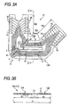
Figs. 1A and 1B , acenter portion 12a of the photodetector conducting wire 12 is divided into two including anouter conducting wire 12A and aninner conducting wire 12B by forming aslit 21 having a predetermined width t along the longitudinal direction of theconducting wire 12 from thecenter portion 12a of the photodetector conducting wire 12 to theother end portion 12c through a boundary K. In addition, the ratio of the width h1 of theouter conducting wire 12A to the width h2 of theinner conducting wire 12B is set to 3 to 1. Since other configurations are approximately the same as those shown inFigs. 4 to 7 , a same reference number is assigned to a same portion, and a description thereof is omitted here. - To describe an example of specific measurements, the width H of the
center portion 12a is 14 mm, the width t of theslit 21 is 2 mm, the width h1 of theouter conducting wire 12A is 9 mm:, and the width h2 of theinner conducting wire 12B is 3 mm. -
Figs, 2A and 2B show major parts of an optical pickup according to a second embodiment of the present invention.Fig. :2A is a development view of a photo detector conducting wire cf the optical pickup, andFig. 2B is a view along arrow B-B ofFig. 2A - As shown in
Figs. 2A and 2B , the ratio of the width h1 of theouter conducting wire 12A to the width h2 of the inner conducting .wire 12B is set to 2 to 1. Since other configurations are approximately the same as those shown inFigs. 1A and 1B , a same reference number is assigned to a same portion, and a description thereof is omitted here. - TO describe an example of specific measurements, the width H of the
center portion 12a is 14 mm, the width t of theslit 21 is 2 mm, the width h1 of theouter conducting wire 12A is 8 mm, and the width h2 of the inner, conductingwire 12B is 4 mm. -
Figs. 3A and 3B show major parts of an optical pickup according to a third embodiment of the present invention.Fig. 3A is a development view of a photo detector conducting wire of the optical pickup, andFig. 3B is a view along arrow C- C ofFig. 3A . - As shown in
Figs. 3A and 3B , the ratio of the width h1 of theouter conducting wire 12A to the width h2 of theinner conducting wire 12B is set to 7 to 5. Since other configurations are approximately the same as those shown in XFigs. 1A and 1B, a same reference number is assigned to a same portion, and a description thereof is omitted here. - To describe an example of specific measurements, the width H of the
center portion 12a is 14 mm, the width t of theslit 21 is 2 mm, the width h1 of theouter conducting wire 12A is 7 mm, and the width h2 of theinner conducting wire 12B is 5 mm. - In the above-described configuration.
Figs. 1A and 1B show a case where the ratio of the width h1 of theouter conducting wire 12A to the width h2 of theinner conducting wire 12B is 3 to 1. (in a detailed example, 9 mm to 3 mm), When the ratio is smaller than 3 to 1, that is, when the width h2 of theinner conducting wire 12B decreases from a state shown inFigs. 1A and 1B , the pulling force P and the compressing force F that are applied to theinner conducting wire 12B do not act on theadhesive agent 14 that supports the photo detector PD1. However, since the width h1 of theouter conducting wire 12A is increased in correspondence with a decrease in the width h2 of theinner conducting wire 12B, the shape of the photo detector conducting wire is approximately the same as the shape of a general photo detector conducting wire shown inFigs. 8A and 8B . Accordingly, the pulling fores P and the compressing force F that are applied to theouter conducting wire 12A become considerably strong, and act on theadhesive agent 14 that supports the photo detector PD1. Therefore, theadhesive agent 14 is deformed in a case where the adhesive agent is exposed in a high-temperature environment such as a curing process or a warehouse. As a result, the three-dimensional adjustment XYZ and rotation adjustment T of the photo detector PD1 may be performed incorrectly, and thereby there is a possibility of generation of a read error. -
Figs. 3A and 3B show a case where the ratio of the width h1 of theouter conducting wire 12A to the width h2 of theinner conducting wire 12B is 7 to 5 (in a detailed example, 7 mm to 5 mm). When the ratio exceeds the ratio of 7 to 5, that is, when the width h2 of theinner conducting wire 12B is increased from a state shown inFigs. 3A and 3B , the width h2 of theinner conducting wire 12B is not quite different from the width h1 of theouter conducting wire 12A. Accordingly, the shape of the photo detector conducting wire is approximately the same as the shape of a general photo detector conducting wire shown inFigs. 9A and 9B . Thus, the pulling force P and the compressing force F that are applied to theInner conducting wire 12B become considerably strong, and act on theadhesive agent 14 that supports the photo detector PD1. Therefore; theadhesive agent 14 is deformed In a case where the adhesive agent is exposed to a high-temperature environment such as a curing process or a warehouse, and accordingly, there is the above-described defect. -
Figs . 2A and 2B show a case where the ratio of the width h1 of theouter conducting wire 12A to the width h2 of theinner conducting wire 12B is 2 to 1 (in a detailed example,8 mm to 4 mm) as an example that is the most appropriate to the present invention. It is preferable that the ratio is in the range of 2.5 to 1 (in the detailed example, 8.6 mm to 3.4 mm) to 1.5 to 1 (in the detailed example, 7.2 mm to 4.8 mm). - According to an embodiment of the present invention, the ratio of the width h1 of the
outer conducting wire 12A to the width h2 of theinner conducting wire 12B is set to be in the range of 3 to 1 (seeFigs. 1A and 1B ) to 7 to 5. (seeFigs. 3A and 3B ) (preferably in the range of 2.5 to 1 to 1.5 to 1 (seeFigs. 2A and 2B )). In addition, by dividing thecenter portion 12a of the photodetector conducting wire 12 into two including theouter conducting wire 12A and theinner conducting wire 12B, the pulling force P and the compression force F that are applied to the photodetector conducting wire 12 are dispersed to both the inner andouter conducting wires inner conducting wire 12B is set to be appropriately smaller than the width h1 of theouter conducting wire 12A. Accordingly, theinner conducting wire 12B can be easily bent in correspondence with a decrease in the width h2, and thus the pulling force P and the compressing force F that are applied to the inner conducting wire decrease. As a result, the pulling force P and the compressing force F that are applied to theinner conducting wire 12B scarcely act on theadhesive agent 14 that supports the photo detector PD1, and accordingly, theadhesive agent 14 is not deformed in a case where the adhesive agent is exposed to a high-temperature environment such as a curing process or a warehouse. Therefore, the three-dimensional adjustment XYZ and rotation adjustment T of the photo detector PD1 can be maintained for a long time, and thus a read error can be prevented. - In
Figs. 1A to 3B , a case where the width t of theslit 21 is set to 2 mm. However, when the width t of theslit 21 is smaller than 1 mm, the width t of theslit 21 is too small. Accordingly, both the inner andouter conducting wires other end portion 12c of the photodetector conducting wire 12 is bent in the boundary K, and thereby there is a possibility that remaining load is applied to theadhesive agent 14. - When the width t of the
slit 21 exceeds. 3 mm, the width t of theslit 21 is too large. Thus, the width h1 + h2 of both the conducting wires. 12A and 12B is decreased in correspondence with an increase in the width of the slit. Therefore, it is difficult to appropriately dispose a plurality of theconnection wires 17 in both the inner andouter conducting wires - According to an embodiment of the present invention, since the width t of the
slit 21 is set in the range of 1 to 3 (preferably in the range of 1.5 to 2.5) mn, the width t of theslit 21 is appropriately set. Accordingly, both the inner andouter conducting wires other end portion 12c of the photodetector conducting wire 12 is bent in the boundary K. In addition, the width h1 + h2 of both the inner andouter conducting wires connection wires 17 can be appropriately disposed in both the inner andouter conducting wires
Claims (6)
- An optical pickup comprising:a slide base adapted to move along a radial direction of a disc and having: a first surface; and a second surface;a first substrate fixed to the first surface and comprising a printed circuit board;a standing frame disposed on the second surface;a second substrate facing the standing frame and comprising a printed circuit board;a laser diode operable to emit a laser beam to the disk and disposed in the standing frame;an optical element supported by the second substrate and adapted to receive a light beam reflected from the disk; anda flexible flat cable including: a first end portion; a second end portion; and a curved portion disposed, between the first end portion and the second end portion, wherein:the first end portion is connected to the first substrate;the flexible flat cable is bent so that the second end portion connected to the second substrate;the curved portion is formed with a slit elongated in a longitudinal direction of the flexible flat cable and defining an outer portion and an inner portion; anda width of the inner portion is narrower than a width of the outer portion.
- The optical pickup according to Claim 1,
wherein the width of the outer portion is 1.4 to 3 times wider than the width of the inner portion. - The optical pickup according to Claim 2,
wherein the width of the outer portion is 1.5 to 2.5 times wider than the width of the inner portion. - The optical pickup according to Claim 1,
wherein the width of the slit falls within a range from 1 mm to 3 mm. - The optical pickup according to Claim 4,
wherein the width of the slit falls within a range from 1.5 to 2.5 mm. - The optical pickup according to Claim 1,
wherein the flexible flat cable is bent at the curved portion.
Applications Claiming Priority (1)
| Application Number | Priority Date | Filing Date | Title |
|---|---|---|---|
| JP2007101547A JP4765987B2 (en) | 2007-04-09 | 2007-04-09 | Optical pickup |
Publications (2)
| Publication Number | Publication Date |
|---|---|
| EP1981026A1 true EP1981026A1 (en) | 2008-10-15 |
| EP1981026B1 EP1981026B1 (en) | 2010-07-28 |
Family
ID=39643848
Family Applications (1)
| Application Number | Title | Priority Date | Filing Date |
|---|---|---|---|
| EP08007070A Expired - Fee Related EP1981026B1 (en) | 2007-04-09 | 2008-04-09 | Optical pickup |
Country Status (4)
| Country | Link |
|---|---|
| US (1) | US7861254B2 (en) |
| EP (1) | EP1981026B1 (en) |
| JP (1) | JP4765987B2 (en) |
| DE (1) | DE602008001915D1 (en) |
Families Citing this family (1)
| Publication number | Priority date | Publication date | Assignee | Title |
|---|---|---|---|---|
| TWI596994B (en) * | 2014-02-20 | 2017-08-21 | Tear-resistant structure of the flexible circuit board |
Citations (2)
| Publication number | Priority date | Publication date | Assignee | Title |
|---|---|---|---|---|
| JPH0430374A (en) * | 1990-05-25 | 1992-02-03 | Olympus Optical Co Ltd | Optical information recording and reproducing device |
| JP2000331372A (en) | 1999-05-18 | 2000-11-30 | Fujitsu Ten Ltd | Light pickup |
Family Cites Families (1)
| Publication number | Priority date | Publication date | Assignee | Title |
|---|---|---|---|---|
| JP3832767B2 (en) * | 2003-10-28 | 2006-10-11 | Tdk株式会社 | Optical pickup device and manufacturing method thereof |
-
2007
- 2007-04-09 JP JP2007101547A patent/JP4765987B2/en not_active Expired - Fee Related
-
2008
- 2008-04-08 US US12/078,915 patent/US7861254B2/en not_active Expired - Fee Related
- 2008-04-09 DE DE602008001915T patent/DE602008001915D1/en active Active
- 2008-04-09 EP EP08007070A patent/EP1981026B1/en not_active Expired - Fee Related
Patent Citations (2)
| Publication number | Priority date | Publication date | Assignee | Title |
|---|---|---|---|---|
| JPH0430374A (en) * | 1990-05-25 | 1992-02-03 | Olympus Optical Co Ltd | Optical information recording and reproducing device |
| JP2000331372A (en) | 1999-05-18 | 2000-11-30 | Fujitsu Ten Ltd | Light pickup |
Also Published As
| Publication number | Publication date |
|---|---|
| US7861254B2 (en) | 2010-12-28 |
| DE602008001915D1 (en) | 2010-09-09 |
| EP1981026B1 (en) | 2010-07-28 |
| JP4765987B2 (en) | 2011-09-07 |
| JP2008257822A (en) | 2008-10-23 |
| US20080247297A1 (en) | 2008-10-09 |
Similar Documents
| Publication | Publication Date | Title |
|---|---|---|
| EP1288692A1 (en) | Structure for connecting a lens to a lens holder without using an adhesive | |
| US20010012162A1 (en) | Pickup device | |
| EP1981026B1 (en) | Optical pickup | |
| JP4371064B2 (en) | Mounting structure of the laser holder to the base member | |
| TWI259632B (en) | Semiconductor laser device and optical pick-up apparatus using semiconductor laser device | |
| EP1675112A3 (en) | Optical pickup actuator and optical recording and/or reproducing apparatus | |
| EP1592000A3 (en) | Laser/detector device for optical recording with adjustable detector position | |
| JP4720710B2 (en) | Optical pickup | |
| US8125877B2 (en) | Optical pickup | |
| JP4854680B2 (en) | Pickup device | |
| JP2009158022A (en) | Optical pickup | |
| JP3832767B2 (en) | Optical pickup device and manufacturing method thereof | |
| JP4133896B2 (en) | Optical pickup device | |
| JP4941005B2 (en) | Skew adjustment mechanism in disk drive device | |
| JP2009010034A (en) | Printed board positioning structure | |
| EP2360691A1 (en) | Disk device | |
| EP1522998A3 (en) | Recording power determining method, program, computer readable storage medium, recording power detemining device, and optical disk apparatus | |
| JP2000207762A (en) | Optical pickup device | |
| JP2006260656A (en) | Objective lens drive unit | |
| JP2007200380A (en) | Manufacturing method of optical pickup device, optical pickup device and electronic equipment | |
| JP2008059712A (en) | Pickup device | |
| JP2003132552A (en) | Optical pickup device | |
| JP2007200403A (en) | Optical pickup | |
| JP2004005841A (en) | Optical pickup device | |
| US20060028958A1 (en) | Alignment apparatus in an optical pickup device |
Legal Events
| Date | Code | Title | Description |
|---|---|---|---|
| PUAI | Public reference made under article 153(3) epc to a published international application that has entered the european phase |
Free format text: ORIGINAL CODE: 0009012 |
|
| AK | Designated contracting states |
Kind code of ref document: A1 Designated state(s): AT BE BG CH CY CZ DE DK EE ES FI FR GB GR HR HU IE IS IT LI LT LU LV MC MT NL NO PL PT RO SE SI SK TR |
|
| AX | Request for extension of the european patent |
Extension state: AL BA MK RS |
|
| 17P | Request for examination filed |
Effective date: 20081229 |
|
| 17Q | First examination report despatched |
Effective date: 20090206 |
|
| AKX | Designation fees paid |
Designated state(s): DE FR GB |
|
| GRAC | Information related to communication of intention to grant a patent modified |
Free format text: ORIGINAL CODE: EPIDOSCIGR1 |
|
| GRAP | Despatch of communication of intention to grant a patent |
Free format text: ORIGINAL CODE: EPIDOSNIGR1 |
|
| GRAS | Grant fee paid |
Free format text: ORIGINAL CODE: EPIDOSNIGR3 |
|
| GRAA | (expected) grant |
Free format text: ORIGINAL CODE: 0009210 |
|
| AK | Designated contracting states |
Kind code of ref document: B1 Designated state(s): DE FR GB |
|
| REG | Reference to a national code |
Ref country code: GB Ref legal event code: FG4D |
|
| REF | Corresponds to: |
Ref document number: 602008001915 Country of ref document: DE Date of ref document: 20100909 Kind code of ref document: P |
|
| PLBE | No opposition filed within time limit |
Free format text: ORIGINAL CODE: 0009261 |
|
| STAA | Information on the status of an ep patent application or granted ep patent |
Free format text: STATUS: NO OPPOSITION FILED WITHIN TIME LIMIT |
|
| 26N | No opposition filed |
Effective date: 20110429 |
|
| REG | Reference to a national code |
Ref country code: DE Ref legal event code: R097 Ref document number: 602008001915 Country of ref document: DE Effective date: 20110429 |
|
| REG | Reference to a national code |
Ref country code: FR Ref legal event code: PLFP Year of fee payment: 9 |
|
| PGFP | Annual fee paid to national office [announced via postgrant information from national office to epo] |
Ref country code: FR Payment date: 20160309 Year of fee payment: 9 |
|
| PGFP | Annual fee paid to national office [announced via postgrant information from national office to epo] |
Ref country code: GB Payment date: 20160406 Year of fee payment: 9 Ref country code: DE Payment date: 20160405 Year of fee payment: 9 |
|
| REG | Reference to a national code |
Ref country code: DE Ref legal event code: R119 Ref document number: 602008001915 Country of ref document: DE |
|
| GBPC | Gb: european patent ceased through non-payment of renewal fee |
Effective date: 20170409 |
|
| REG | Reference to a national code |
Ref country code: FR Ref legal event code: ST Effective date: 20171229 |
|
| PG25 | Lapsed in a contracting state [announced via postgrant information from national office to epo] |
Ref country code: DE Free format text: LAPSE BECAUSE OF NON-PAYMENT OF DUE FEES Effective date: 20171103 Ref country code: FR Free format text: LAPSE BECAUSE OF NON-PAYMENT OF DUE FEES Effective date: 20170502 |
|
| PG25 | Lapsed in a contracting state [announced via postgrant information from national office to epo] |
Ref country code: GB Free format text: LAPSE BECAUSE OF NON-PAYMENT OF DUE FEES Effective date: 20170409 |