EP1973175A1 - Light emitting device and illumination instrument - Google Patents
Light emitting device and illumination instrument Download PDFInfo
- Publication number
- EP1973175A1 EP1973175A1 EP06835023A EP06835023A EP1973175A1 EP 1973175 A1 EP1973175 A1 EP 1973175A1 EP 06835023 A EP06835023 A EP 06835023A EP 06835023 A EP06835023 A EP 06835023A EP 1973175 A1 EP1973175 A1 EP 1973175A1
- Authority
- EP
- European Patent Office
- Prior art keywords
- light emitting
- arrays
- voltage
- input terminals
- semiconductor light
- Prior art date
- Legal status (The legal status is an assumption and is not a legal conclusion. Google has not performed a legal analysis and makes no representation as to the accuracy of the status listed.)
- Withdrawn
Links
- 238000005286 illumination Methods 0.000 title 1
- 238000003491 array Methods 0.000 claims abstract description 122
- 239000004065 semiconductor Substances 0.000 claims description 137
- 239000000758 substrate Substances 0.000 claims description 20
- 230000004048 modification Effects 0.000 description 11
- 238000012986 modification Methods 0.000 description 11
- 229910052737 gold Inorganic materials 0.000 description 7
- 238000010586 diagram Methods 0.000 description 5
- 238000002955 isolation Methods 0.000 description 5
- 229910002704 AlGaN Inorganic materials 0.000 description 4
- VYPSYNLAJGMNEJ-UHFFFAOYSA-N Silicium dioxide Chemical compound O=[Si]=O VYPSYNLAJGMNEJ-UHFFFAOYSA-N 0.000 description 4
- 238000009413 insulation Methods 0.000 description 4
- 238000007747 plating Methods 0.000 description 4
- 229910002482 Cu–Ni Inorganic materials 0.000 description 2
- 229910001030 Iron–nickel alloy Inorganic materials 0.000 description 2
- 239000000853 adhesive Substances 0.000 description 2
- 230000001070 adhesive effect Effects 0.000 description 2
- 229910045601 alloy Inorganic materials 0.000 description 2
- 239000000956 alloy Substances 0.000 description 2
- 230000004888 barrier function Effects 0.000 description 2
- 229910052681 coesite Inorganic materials 0.000 description 2
- 229910052906 cristobalite Inorganic materials 0.000 description 2
- 239000002019 doping agent Substances 0.000 description 2
- 238000005530 etching Methods 0.000 description 2
- 238000004519 manufacturing process Methods 0.000 description 2
- 229910052759 nickel Inorganic materials 0.000 description 2
- 239000011347 resin Substances 0.000 description 2
- 229920005989 resin Polymers 0.000 description 2
- 239000000377 silicon dioxide Substances 0.000 description 2
- 229910052682 stishovite Inorganic materials 0.000 description 2
- 229910052905 tridymite Inorganic materials 0.000 description 2
- CYJRNFFLTBEQSQ-UHFFFAOYSA-N 8-(3-methyl-1-benzothiophen-5-yl)-N-(4-methylsulfonylpyridin-3-yl)quinoxalin-6-amine Chemical compound CS(=O)(=O)C1=C(C=NC=C1)NC=1C=C2N=CC=NC2=C(C=1)C=1C=CC2=C(C(=CS2)C)C=1 CYJRNFFLTBEQSQ-UHFFFAOYSA-N 0.000 description 1
- 230000000694 effects Effects 0.000 description 1
- 230000020169 heat generation Effects 0.000 description 1
- 229910052745 lead Inorganic materials 0.000 description 1
Images




Classifications
-
- H—ELECTRICITY
- H05—ELECTRIC TECHNIQUES NOT OTHERWISE PROVIDED FOR
- H05B—ELECTRIC HEATING; ELECTRIC LIGHT SOURCES NOT OTHERWISE PROVIDED FOR; CIRCUIT ARRANGEMENTS FOR ELECTRIC LIGHT SOURCES, IN GENERAL
- H05B45/00—Circuit arrangements for operating light-emitting diodes [LED]
-
- H—ELECTRICITY
- H05—ELECTRIC TECHNIQUES NOT OTHERWISE PROVIDED FOR
- H05B—ELECTRIC HEATING; ELECTRIC LIGHT SOURCES NOT OTHERWISE PROVIDED FOR; CIRCUIT ARRANGEMENTS FOR ELECTRIC LIGHT SOURCES, IN GENERAL
- H05B45/00—Circuit arrangements for operating light-emitting diodes [LED]
- H05B45/40—Details of LED load circuits
- H05B45/42—Antiparallel configurations
-
- Y—GENERAL TAGGING OF NEW TECHNOLOGICAL DEVELOPMENTS; GENERAL TAGGING OF CROSS-SECTIONAL TECHNOLOGIES SPANNING OVER SEVERAL SECTIONS OF THE IPC; TECHNICAL SUBJECTS COVERED BY FORMER USPC CROSS-REFERENCE ART COLLECTIONS [XRACs] AND DIGESTS
- Y02—TECHNOLOGIES OR APPLICATIONS FOR MITIGATION OR ADAPTATION AGAINST CLIMATE CHANGE
- Y02B—CLIMATE CHANGE MITIGATION TECHNOLOGIES RELATED TO BUILDINGS, e.g. HOUSING, HOUSE APPLIANCES OR RELATED END-USER APPLICATIONS
- Y02B20/00—Energy efficient lighting technologies, e.g. halogen lamps or gas discharge lamps
- Y02B20/30—Semiconductor lamps, e.g. solid state lamps [SSL] light emitting diodes [LED] or organic LED [OLED]
Definitions
- the present invention relates to a light emitting unit including a plurality of semiconductor light emitting devices formed on a same substrate and a lighting apparatus.
- a light emitting unit including a plurality of semiconductor light emitting devices on a same substrate is hitherto been known.
- Patent Literature 1 disclosed a light emitting unit 200 including light emitting arrays 202 having semiconductor light emitting devices 201a and 201b provided on a same substrate.
- the semiconductor light emitting devices 201a of the light emitting arrays 202 are arranged in such a manner that the direction of current flowing through the light emitting arrays 201a is opposite to that of the light emitting arrays 201b.
- the light emitting unit 200 is provided with two common voltage input terminals 203a and 203b at both ends of the both light emitting arrays 202 and is connected to an AC power supply P through these voltage input terminals 203a and 203b.
- the light emitting unit 200 of the aforementioned Patent Literature 1 is provided with only the two voltage input terminals 203a and 203b and can handle only a single voltage. Accordingly, if voltage higher than specified voltage is applied to the voltage input terminals 203a and 203b, overvoltage applied to the individual semiconductor light emitting devices 201a and 201b causes current exponentially increased to flow through the semiconductor light emitting devices 201a and 201b. This gives damage in the semiconductor light emitting devices 201a and 201b or shortens the life thereof. On the contrary, if voltage lower than the specified voltage is applied to the voltage input terminals 203a and 203b, the semiconductor light emitting devices 201a and 201b do not emit light or, if emitting light, the emitted light is weak.
- the semiconductor light emitting devices 201a and 201b cannot be turned on while the applied voltage is less than a certain threshold value V t . Accordingly, even if the AC power Pe shown in FIG. 19 is applied, the light emitting devices 201a and 201b are not turned on between times t e1 and t e2 when the absolute value of the applied voltage is not more than the threshold voltage V t .
- the light emitting unit 200 therefore has a problem of long off time when either of the semiconductor light emitting devices 201a and 201b does not emit light and that causes significant flicker.
- the present invention was made to solve the aforementioned problems, and an object of the present invention is to provide a light emitting unit and a lighting apparatus which can handle different voltages or to provide a light emitting unit with any of the semiconductor light emitting devices being on for long time.
- the voltage input terminals allow the light emitting arrays to be brought into serial or parallel connections to each other in order that the specified voltage is applied to each light emitting array.
- An invention according to claim 2 is the light emitting unit of claim 1 in which each of the light emitting arrays includes a same number of the semiconductor light emitting devices.
- An invention according to claim 3 is the light emitting unit of any one of claims 1 and 2, in which each of the light emitting arrays includes the 2M semiconductor light emitting devices and the M semiconductor light emitting devices are connected to allow current to flow therethrough in a direction opposite to that of the remaining M semiconductor light emitting arrays.
- An invention according to claim 4 is the light emitting unit of any one of claims 1 to 3, in which the number of the light emitting arrays is two and the number of the voltage input terminals is three.
- the switching controller causes the light emitting arrays to be connected in parallel or in series to set voltage applied to each of the light emitting arrays to the specified voltage and automatically switches the voltage input terminals to which the voltage is inputted.
- An invention according to claim 6 is a light emitting unit including: three light emitting arrays each including one or a plurality of semiconductor light emitting devices formed on a same substrate; and three power input terminals which are provided at ends of the respective light emitting arrays and are supplied with a three-phase AC power supply.
- the power input terminals are individually supplied with three types of AC power with different phases.
- An invention according to claim 7 is the light emitting unit according to claim 6, in which the other ends of the three light emitting arrays are electrically connected to each other and grounded.
- An invention according to claim 8 is the light emitting unit according to any one of claims 6 and 7, in which at least any one of the three light emitting arrays is supplied with voltage not less than a threshold voltage necessary to light the light emitting array.
- An invention according to claim 9 is the light emitting unit according to any one of claims 6 to 8, in which each of the light emitting arrays includes the 2M semiconductor light emitting devices and the M semiconductor light emitting devices are connected to allow current to flow therethrough in a direction opposite to that of the remaining the M semiconductor light emitting devices.
- An invention according to claim 10 is the light emitting unit according to any one of claims 6 to 9, in which each of the light emitting arrays includes a same number of the semiconductor light emitting devices.
- the light emitting unit of the present invention by providing the (N+1) or more voltage input terminals corresponding to the ends of the N light emitting arrays, according to the applied voltage, the voltage input terminals connected to the power supply can be selected and the voltage input terminals can be connected to each other.
- the specified voltage of the light emitting arrays can be supplied to each light emitting array. For different applied voltages, it is possible to prevent damage of the semiconductor light emitting device of the light emitting arrays due to overvoltage and moreover and to prevent non-light emission of the semiconductor light emitting devices due to low voltage, thus allowing the semiconductor light emitting devices to emit properly.
- the switching controller capable of switching the voltage input terminals of the light emitting unit.
- the voltage input terminals to which the voltage is inputted can be therefore automatically connected to the power supply or connected to each other based on the applied voltage. Accordingly, a user can easily connect the lighting apparatus to a power supply regardless of the applied voltage.
- the three power input terminals provided at the ends of the light emitting arrays are supplied with three types of AC power with different phases from the three-phase AC power supply. It is therefore possible to increase time when the voltage not less than the threshold voltage of the light emitting arrays is applied to at least one of the light emitting arrays. Accordingly, the time when at least one of the three light emitting arrays is lighted can be increased. It is therefore possible to increase lighting time of the lighting apparatus and to prevent flickering.
- FIG. 1 is an entire constitutional view of a lighting apparatus including a light emitting unit according to the first embodiment of the present invention.
- FIG. 2 is a circuit diagram of a lighting apparatus before connecting to a power supply yet.
- FIG. 3 is a schematic plan view of one of semiconductor light emitting devices constituting the light emitting unit.
- FIG. 4 is a cross-sectional view of some of the semiconductor light emitting devices constituting the light emitting unit.
- a lighting apparatus 1 includes a switching controller 2 and a light emitting unit 2.
- the switching controller 2 includes two input terminals 11a and 11b to which electrical power is inputted from an AC power supply P and three output terminals 12a to 12c through which power is outputted to the light emitting unit 3.
- the switching controller 2 is configured to automatically switch connection between the input terminals 11a and 11b and the output terminals 12a to 12c based on voltage supplied from an AC power supply P so that voltage applied to the later-described light emitting arrays 21a and 21b becomes the specified voltage.
- the light emitting unit 3 includes two light emitting arrays 21a and 21b which are formed on a same substrate 31 bonded to an insulating package (not shown) and three voltage input terminals 22a to 22c.
- the substrate 31 is bonded to the package by an insulating resin adhesive.
- Each of the light emitting arrays 21a and 21b is configured to handle a voltage of 100 V (specified voltage). Accordingly, the two light emitting arrays 21a and 21b connected in series can handle a voltage of 200 V.
- each of the light emitting arrays 21a and 21b includes twelve semiconductor light emitting devices (light emitting elements, light emitting diodes) 23a and 23b formed on the same substrate 31 and wiring films 24 to connect the semiconductor light emitting devices 23a and 23b.
- the six semiconductor light emitting devices 23a and six semiconductor light emitting devices 23b are arranged with pn junctions oppositely oriented so that current flows in opposite directions.
- the p sides of the six semiconductor light emitting devices 23a are connected to the n sides of the adjacent semiconductor light emitting devices 23a by the wiring films 24 so that the six semiconductor light emitting devices 23a are connected in series.
- the p sides of the six semiconductor light emitting devices 23b are connected to the n sides of the adjacent semiconductor light emitting devices 23b by the wiring films 24 so that the six semiconductor light emitting devices 23b are also connected in series.
- the six semiconductor light emitting devices 23a and the remaining six semiconductor light emitting devices 23b are connected in series so that current flows in directions opposite to each other.
- any ones of the semiconductor light emitting devices 23a and 23b can be always turned on.
- auxiliary wiring films 24a are provided across the wiring films 24 connecting pairs of the semiconductor light emitting devices 23a and 23b and adjacent pairs of the semiconductor light emitting devices 23a and 23b.
- Each of the semiconductor light emitting devices 23a and 23b includes the substrate 31 and a semiconductor stack 32 formed on the substrate 31.
- the semiconductor stack 32 includes a low temperature buffer layer 33, a high temperature buffer layer 34, an n-type semiconductor layer 35, an MQW active layer 36, a p-type semiconductor layer 37, and a transparent electrode 38.
- the low temperature buffer layer 33 is composed of a GaN layer with a thickness of about 0.005 to 0.1 ⁇ m.
- the high temperature buffer layer 34 is composed of an undoped GaN layer with a thickness of about 1 to 3 ⁇ m.
- the high temperature buffer layer 34 is semi-insulating for insulation of the semiconductor light emitting devices 23a and 23b.
- the n-type semiconductor layer 35 includes an about 1 to 5 ⁇ m thick contact layer composed of an n-GaN layer doped with Si as an n-type dopant and a confinement layer composed of an n-AlGaN layer.
- Part of the MQW active layer 36, p-type semiconductor layer 37, and transparent electrode 38 are etched so as to expose a part of the contact layer of the n-type semiconductor layer 35.
- the MQW active layer is composed of a multi-quantum well structure with a thickness of about 0.05 to 0.3 ⁇ m.
- the MQW active layer 36 has a band gap energy smaller than that of the confinement layer and includes three to eight pairs of about 1 to 3 nm thick well layers of In 0.13 Ga 0.87 N and barrier layers composed of about 10 to 20 nm thick GaN layers which are stacked on each other.
- the p-type semiconductor layer 37 has a thickness of about 0.2 to 1.0 ⁇ m and includes a confinement layer composed of a p-AlGaN layer and a contact layer composed of a p-GaN layer.
- the transparent electrode 38 is capable of transmitting light emitted by the MQW active layer 36 and is formed on the upper surface of the p-type semiconductor layer 37.
- the transparent electrode 38 is composed of a 0.01 to 0.5 ⁇ m thick ZnO layer.
- the transparent electrode 38 may be composed of ITO, an thin alloy layer of Ni and Au, or the like.
- Isolation trenches 39 with a width of about 0.6 to 5 ⁇ m are formed between adjacent pairs of the semiconductor light emitting devices 23a and 23b by etching a part of the high temperature buffer layer 34, the n-type semiconductor layer 35, the MQW active layer 36, the p-type semiconductor layer 37, and the transparent electrode 38.
- insulating films 40 composed of SiO 2 are formed for insulation of the adjacent semiconductor light emitting devices 23a and 23b.
- the wiring films 24 are formed over the insulating films 40.
- Each of The wiring films 24 is composed of an about 0.3 to 1.0 ⁇ m thick metallic film of Au or Al, or the like.
- the voltage input terminals 22a to 22c are composed of Fe-Ni plating or Cu-Ni plating.
- the voltage input terminals 22a and 22c are connected to ends of the light emitting arrays 21a and 21b through pad electrodes 25a and 25c.
- the voltage input terminal 22b is connected through the pad electrode 25b to a part connected to the ends of the light emitting arrays 21a and 21b.
- the voltage input terminals 22a to 22c are connected to the pad electrodes 25a to 25c through Au or Al wires.
- the light emitting unit 3 is manufactured by a known semiconductor manufacturing method or the like.
- FIG. 5 is an operation explanatory view in the case where the lighting apparatus is connected to the 200 V AC power supply.
- FIG. 6 is an operation explanatory view in the case where the lighting apparatus is connected to the 100 V AC power supply.
- the output terminals 12a to 12c of the switching controller 2 are not connected to the input terminals 11a and 11b.
- the lighting apparatus 1 when the lighting apparatus 1 is connected to a 100 V AC power supply P 100 , the voltage input terminals 22a and 22c are connected to the input terminal 11a through the output terminals 12a and 12c, respectively, and the voltage input terminal 22b is connected to the input terminal 11b through the output terminal 12b.
- the light emitting unit is in the condition where the light emitting arrays 21a and 21b are connected in parallel. Accordingly, the specified voltage of 100 V is applied to the both ends of each of the light emitting arrays 21a and 22b, thus allowing the light emitting unit 3 to normally operate.
- the light emitting unit 3 includes the three voltage input terminals 22a to 22c corresponding to the two light emitting arrays 21a and 21b. It is therefore possible to select the voltage input terminals 22a to 22c connected to the AC power supply P or connect the voltage input terminals 22a to 22c to each other according to the supplied voltage.
- the light emitting unit 3 can be connected to the AC power supply P with the light emitting arrays 21a and 21b connected to each other in series or in parallel. Accordingly, voltage applied to each of the light emitting arrays 21a and 21b can be 100 V as the specified voltage of the light emitting arrays 21a and 21b. It is therefore possible to apply a same voltage to the light emitting arrays 21a and 21b despite the difference supplied voltage. Accordingly it is possible to prevent heat generation and damage of the semiconductor light emitting devices 23a and 23b due to overvoltage and emit light at equal illuminance.
- the lighting apparatus 1 is provided with the switching controller 2 which is capable of automatically switching connections between the voltage input terminals 22a to 22c of the light emitting unit 3 and the AC power supply. Accordingly, based on the applied voltage, the voltage input terminals 22a to 22c to which the voltage is applied can be automatically connected to the AC power supply P and the voltage input terminals 22a to 22c are connected to each other. A user can therefore easily connect the lighting apparatus 1 to the AC power supply P regardless of the supplied voltage.
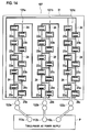
- FIG. 14 is an entire constitutional view of a light emitting unit according to of the second embodiment of the present invention.
- FIG. 15 is a circuit configuration diagram of the light emitting unit.
- a light emitting unit 101 includes three light emitting arrays 121a to 121c and three power input terminals 122a to 122c, which are formed on the same substrate 31 bonded to an insulating package (not shown).
- the substrate 31 is bonded to the package by an insulating resin adhesive.
- each of the light emitting arrays 121a to 121c includes ten semiconductor light emitting devices (light emitting diodes) 23a and 23b formed on the same substrate 31 and wiring films 24 connecting the semiconductor light emitting devices 23a and 23b.
- the five semiconductor light emitting devices 23a and five semiconductor light emitting devices 23b are arranged with the pn junctions oppositely oriented so that current flows therethrough in the opposite directions.
- the p-sides of the semiconductor light emitting devices 23a are connected to the n-sides of the adjacent semiconductor light emitting devices 23a through the wiring films 24 so that the five semiconductor light emitting devices 23a are connected in series.
- the p-sides of the semiconductor light emitting devices 23b are connected to the n-sides of the adjacent semiconductor light emitting devices 23b through the wiring films 24 so that the five semiconductor light emitting devices 23b are also connected in series.
- the six semiconductor light emitting devices 23a and the remaining six semiconductor light emitting devices 23b are connected in series so that current flows in the opposite directions.
- auxiliary wiring films 24a are provided across the wiring films 24 which individually connect pairs of the semiconductor light emitting devices 23a and 23b and adjacent pairs of the semiconductor light emitting devices 23a and 23b.
- Each of the semiconductor light emitting devices 23a and 23b includes the substrate 31 and a semiconductor stack 32 formed on the substrate 31.
- the semiconductor stack 32 includes a low temperature buffer layer 33, a high temperature buffer layer 34, an n-type semiconductor layer 35, an MQW active layer 36, a p-type semiconductor layer 37, and a transparent electrode 38.
- the low temperature buffer layer 33 is composed of a GaN layer with a thickness of about 0.005 to 0.1 ⁇ m.
- the high temperature buffer layer 34 is composed of an undoped GaN layer with a thickness of about 1 to 3 ⁇ m.
- the high temperature buffer layer 34 is semi-insulating for insulation of the semiconductor light emitting devices 23a and 23b.
- the n-type semiconductor layer 35 includes an about 1 to 5 ⁇ m thick contact layer composed of an n-GaN layer doped with Si as an n-type dopant and a confinement layer composed of an n-AlGaN layer.
- Part of the MQW active layer 36, p-type semiconductor layer 37, and transparent electrode 38 are etched so as to expose a part of the contact layer of the n-type semiconductor layer 35.
- the MQW active layer is composed of a multi-quantum well structure with a thickness of about 0.05 to 0.3 ⁇ m.
- the MQW active layer 36 has a band gap energy smaller than that of the confinement layer and includes three to eight pairs of about 1 to 3 nm thick well layers of In 0.13 Ga 0.87 N and barrier layers composed of about 10 to 20 nm thick GaN layers which are stacked on each other.
- the p-type semiconductor layer 37 has a thickness of about 0.2 to 1.0 ⁇ m and includes a confinement layer composed of a p-AlGaN layer and a contact layer composed of a p-GaN layer.
- the transparent electrode 38 is capable of transmitting light emitted by the MQW active layer 36 and is formed on the upper surface of the p-type semiconductor layer 37.
- the transparent electrode 38 is composed of a 0.01 to 0.5 ⁇ m thick ZnO layer.
- the transparent electrode 38 may be composed of ITO, an thin alloy layer of Ni and Au, or the like.
- Isolation trenches 39 with a width of about 0.6 to 5 ⁇ m are formed between adjacent pairs of the semiconductor light emitting devices 23a and 23b by etching a part of the high temperature buffer layer 34, the n-type semiconductor layer 35, the MQW active layer 36, the p-type semiconductor layer 37, and the transparent electrode 38.
- insulating films 40 composed of SiO 2 are formed for insulation of the adjacent semiconductor light emitting devices 23a and 23b.
- the wiring films 24 are formed over the insulating films 40.
- Each of The wiring films 24 is composed of an about 0.3 to 1.0 ⁇ m thick metallic film of Au or Al, or the like.
- Voltage input terminals 122a to 122c are composed of Fe-Ni plating or Cu-Ni plating.
- the power input terminal 122a is connected through the pad electrode 25a to an end of the light emitting array 121a and the other end of the light emitting array 121c.
- the power input terminal 122b is connected through the pad electrode 25b to an end of the light emitting array 121b and the other end of the light emitting array 121a.
- the power input terminal 122c is connected through the pad electrode 25c to an end of the light emitting array 121c and the other end of the light emitting array 121b.
- the power input terminals 122a to 122c are connected to the pad electrodes 25a to 25c through Au or Al wires.
- the power input terminals 122a to 122c are connected to output terminals 112a to 112c of a three-phase AC power supply P, respectively.
- the three-phase AC power supply thus supplies AC powers with different phases to the individual light emitting arrays 121a to 121c through the power input terminals 122a to 122c.
- the aforementioned light emitting unit 101 is manufactured by a known semiconductor manufacturing method or the like.
- FIG. 16 is a voltage-time relationship diagram of AC powers supplied to the light emitting arrays.
- AC powers Pa, Pb, and Pc shown in FIGS. 16(a), 16(b), and 16(c) are supplied to the light emitting arrays 121a, 121b, and 121c, respectively.
- the AC powers Pa to Pc supplied to the light emitting arrays 121a to 121c are different in phase by one third of period T.
- V t and -V t are threshold voltages necessary to cause the semiconductor light emitting devices 23a and 23b of the light emitting arrays 121a to 121c to emit light.
- the voltage supplied to the light emitting array 121a becomes V t or less, and the light emitting array 121a turns off.
- the light emitting array 121c is continuously lighted, and the light emitting unit 101 does not black out.
- the voltage supplied to the light emitting array 121b becomes V t or more, the light emitting array 121b lights up.
- the light emitting array 121c is continuously lighted, and the light emitting arrays 121b and 121c are both lighted at and after the time t b1 .
- the voltage supplied to the light emitting array 121c becomes -V t or more, and the light emitting array 121c turns off.
- the light emitting arrays 121b is continuously lighted, and the light emitting unit 101 does not black out.
- the light emitting unit 101 is provided with the three light emitting arrays 121a to 121c and the three power input terminals 122a to 122c at the ends of the respective light emitting arrays 121a to 121c for connection of the three-phase AC power supply P, so that three powers with different phases can be supplied to the light emitting arrays 121a to 121c.
- This allows any one or two of the light emitting arrays 121a to 121c to be always supplied with voltage whose absolute value is not less than the threshold voltage V t .
- any one or two of the light emitting arrays 121a to 121c can keep lighted, and the light emitting unit 101 can be always lighted. It is therefore possible to prevent flickering and the like of the light emitting unit 101.
- the light emitting unit 3 is configured to be included in the lighting apparatus 1 but may be configured to be a separate unit.
- both of the light emitting arrays 21a and 21b light up also when the light emitting unit 3 is connected to the 100 V AC power supply.
- the light emitting unit 3 may be configured so that any one of the light emitting arrays 21a and 21b lights up when the light emitting unit 3 is connected to the 100 V AC power supply. In such a case, any one of the voltage input terminals 22a and 22c and the voltage input terminal 22b should be connected to the 100V AC power supply.
- the light emitting unit 3 is provided with the two light emitting arrays 21a and 21b, but the light emitting unit may be provided with three or more light emitting arrays.
- a light emitting unit 3A may include four light emitting arrays 51a to 51d. An end of each of the light emitting arrays 51a to 51d is connected to any two of the voltage input terminals 52a to 52h.
- the lighting apparatus 1A includes a switching controller 2A having output terminals 53a to 53h corresponding to the voltage input terminals 52a to 52h and input terminals 54a and 54b to which AC power supply is given.
- the switching controller 2A connects the voltage input terminals 52b, 52d, and 52f to the voltage input terminals 52c, 52e, and 52g, respectively, to connect the four light emitting arrays 51a to 51d in series.
- the voltage input terminals 52a and 52h are connected to the AC power supply P 200 through the input terminals 54a and 54b, so that each of the light emitting arrays 51a to 51d is supplied with the specified voltage of 50 V and can be normally operated.
- the switching controller 2A connects the voltage input terminal 52b to the voltage input terminal 52c to connect the light emitting arrays 51a and 51b in series and connects the voltage input terminal 52f to the voltage input terminal 52g to connect the light emitting arrays 51c and 51d in series. Furthermore, the switching controller 2A connects the voltage input terminals 52a and 52d to the voltage input terminal 52e and 52h, respectively, to connect in parallel the light emitting arrays 51a and 51b connected in series to the light emitting arrays 51c and 51d connected in series.
- the voltage input terminals 52a and 52e and the voltage input terminals 52d and 52h are connected to the AC power supply P 100 through the input terminals 54a and 54b, respectively. Accordingly, the specified voltage of 50 V is applied to each of the light emitting arrays 51a to 51d, and the light emitting arrays 51a to 51d can normally operate.
- the switching controller 2A connects the voltage input terminals 52a, 52c, 52e, and 52g to each other and connects the voltage input terminals 52b, 52d, 52f, and 52h to each other to connect all the light emitting arrays 51a to 51d in parallel.
- the switching controller 2A connects the voltage input terminals 52a, 52c, 52e, and 52g and the voltage input terminals 52b, 52d, 52f, and 52h to the AC power supply P 50 through the input terminals 54a and 54b, respectively.
- the specified voltage of 50 V is thus applied to each of the light emitting arrays 51a to 51d, and the light emitting arrays 51a to 51d can normally operate.
- the present invention may be applied to a lighting apparatus and a light emitting unit which are connected to a DC power supply.
- semiconductor light emitting devices 23a of the light emitting arrays 61a and 61b are connected so that current flows therethrough in the same direction.
- voltage input terminals 62a to 62d are provided at the both ends of the light emitting arrays 61a and 61b. Accordingly, the voltage input terminals 62a to 62d are connected to a DC power supply so that current flows through the light emitting arrays 61a and 61b in a specified direction.
- the lighting apparatus 1B includes a switching controller 2B having input terminals 63a and 63b which are connected to a DC power supply P' 200 or P' 100 and output terminals 64a to 64d which are connected to the voltage input terminals 62a to 62d.
- the switching controller 2B connects the voltage input terminals 62b to the voltage input terminal 62c to connect the light emitting arrays 61a and 61b in series. In this state, the switching controller 2B connects the voltage input terminals 62a and 62d to the DC power supply P' 100 , so that the specified voltage of 100 V is applied to each of the light emitting arrays 61a and 61b.
- the light emitting arrays 61a and 61b can therefore normally operate.
- the switching controller 2B connects the voltage input terminals 62a and 62b to the voltage input terminals 62c and 62d, respectively, to connect the light emitting arrays 61a and 61b in parallel.
- the switching controller 2B connects the voltage input terminals 62a and 62c and voltage input terminals 62d and 62b to the DC power supply P' 100 , so that the specified voltage of 100 V is applied to each of the light emitting arrays 61a and 61b.
- the light emitting arrays 61a and 61b can therefore normally operate.
- the numbers of light emitting arrays and voltage input terminals should not be especially limited to those of the aforementioned first embodiment.
- the configurations and numbers of the semiconductor light emitting devices 23a and 23b shown in the aforementioned first embodiment are just examples and can be properly changed depending on the desired supplied voltage.
- the power supplies of 100 V and 200 V are switched.
- the switching may be performed based on another voltage value between 100 and 200 V, for example 110 V while all the light emitting arrays are not caused to emit light.
- the other ends of the light emitting arrays 121a, 121b, and 121c are connected to the power input terminals 122b, 122c, and 122a, respectively, but the light emitting unit may be configured as shown in FIG. 17 .
- the other ends of the light emitting arrays 121a to 121c are connected to each other by an auxiliary wiring film 24b, and a pad electrode 25d is formed in the middle of the auxiliary film 24b.
- the pad electrode 25d is connected to a ground terminal 22d grounded through an Au or Al wire. The other ends of the light emitting arrays 121a to 121c are thus grounded through the ground terminal 22d.
- the configurations and numbers of the semiconductor light emitting devices 23a and 23b shown in the aforementioned second embodiment are just examples and can be properly changed depending on the desired supplied voltage.
- the threshold voltage V t is set so that the light emitting unit 101 is always lighted but may be set so that the light emitting unit 101 temporarily blacks out.
Landscapes
- Led Devices (AREA)
- Arrangements Of Lighting Devices For Vehicle Interiors, Mounting And Supporting Thereof, Circuits Therefore (AREA)
Abstract
To provide a light emitting unit and a lighting apparatus capable of handling different voltages.
A lighting apparatus 1 includes a switching controller 2 and a light emitting unit 3. The light emitting unit 3 includes two light emitting arrays 21a and 21b and three voltage input terminals 22a to 22c. The switching controller 2 switches connection of the voltage input terminals 22a to 22c according to a supplied voltage of a power supply to connect the light emitting arrays 21a and 21b in parallel or series. A specified voltage is thus applied to the light emitting arrays 21a and 21b.
Description
- The present invention relates to a light emitting unit including a plurality of semiconductor light emitting devices formed on a same substrate and a lighting apparatus.
- A light emitting unit including a plurality of semiconductor light emitting devices on a same substrate is hitherto been known.
- For example, as shown in
FIG. 18 ,Patent Literature 1 disclosed alight emitting unit 200 includinglight emitting arrays 202 having semiconductorlight emitting devices light emitting unit 200, the semiconductorlight emitting devices 201a of thelight emitting arrays 202 are arranged in such a manner that the direction of current flowing through thelight emitting arrays 201a is opposite to that of thelight emitting arrays 201b. Thelight emitting unit 200 is provided with two commonvoltage input terminals light emitting arrays 202 and is connected to an AC power supply P through thesevoltage input terminals - When AC power Pe shown in
FIG. 19 is supplied by the AC power supply P between thevoltage input terminals light emitting unit 200, the semiconductorlight emitting devices 201a emit light while the applied voltage is positive, and the other semiconductorlight emitting devices 201b emit light while the applied voltage is negative. By causing the semiconductorlight emitting devices light emitting arrays 202 are off to a certain extent in thelight emitting unit 200.
[Patent Literature 1] Japanese Patent Laid-open Publication No.2004-6582 - However, the
light emitting unit 200 of theaforementioned Patent Literature 1 is provided with only the twovoltage input terminals voltage input terminals light emitting devices light emitting devices light emitting devices voltage input terminals light emitting devices - Moreover, even if forward voltage is applied to the semiconductor
light emitting devices light emitting devices FIG. 19 is applied, thelight emitting devices light emitting unit 200 therefore has a problem of long off time when either of the semiconductorlight emitting devices - The present invention was made to solve the aforementioned problems, and an object of the present invention is to provide a light emitting unit and a lighting apparatus which can handle different voltages or to provide a light emitting unit with any of the semiconductor light emitting devices being on for long time.
- To achieve the aforementioned object, an invention according to
claim 1 is a semiconductor light emitting unit, including: N light emitting arrays (N>=2) each including one or a plurality of semiconductor light emitting devices formed on a same substrate, the light emitting arrays having same specified voltage; and at least (N+1) voltage input terminals provided corresponding to ends of the individual light emitting arrays. The voltage input terminals allow the light emitting arrays to be brought into serial or parallel connections to each other in order that the specified voltage is applied to each light emitting array. - An invention according to
claim 2 is the light emitting unit ofclaim 1 in which each of the light emitting arrays includes a same number of the semiconductor light emitting devices. - An invention according to
claim 3 is the light emitting unit of any one ofclaims - An invention according to claim 4 is the light emitting unit of any one of
claims 1 to 3, in which the number of the light emitting arrays is two and the number of the voltage input terminals is three. - A invention according to claim 5 is a lighting apparatus, including: a light emitting unit having N light emitting arrays (N>=2) having one or a plurality of semiconductor light emitting devices formed on a same substrate, the light emitting arrays having same specified voltage, and at least (N+1) voltage input terminals provided corresponding to ends of the individual light emitting arrays; and switching controller switching the voltage input terminals. According to voltage applied to the light emitting unit, the switching controller causes the light emitting arrays to be connected in parallel or in series to set voltage applied to each of the light emitting arrays to the specified voltage and automatically switches the voltage input terminals to which the voltage is inputted.
- An invention according to claim 6 is a light emitting unit including: three light emitting arrays each including one or a plurality of semiconductor light emitting devices formed on a same substrate; and three power input terminals which are provided at ends of the respective light emitting arrays and are supplied with a three-phase AC power supply. The power input terminals are individually supplied with three types of AC power with different phases.
- An invention according to claim 7 is the light emitting unit according to claim 6, in which the other ends of the three light emitting arrays are electrically connected to each other and grounded.
- An invention according to
claim 8 is the light emitting unit according to any one of claims 6 and 7, in which at least any one of the three light emitting arrays is supplied with voltage not less than a threshold voltage necessary to light the light emitting array. - An invention according to claim 9 is the light emitting unit according to any one of claims 6 to 8, in which each of the light emitting arrays includes the 2M semiconductor light emitting devices and the M semiconductor light emitting devices are connected to allow current to flow therethrough in a direction opposite to that of the remaining the M semiconductor light emitting devices.
- An invention according to claim 10 is the light emitting unit according to any one of claims 6 to 9, in which each of the light emitting arrays includes a same number of the semiconductor light emitting devices.
- According to the light emitting unit of the present invention, by providing the (N+1) or more voltage input terminals corresponding to the ends of the N light emitting arrays, according to the applied voltage, the voltage input terminals connected to the power supply can be selected and the voltage input terminals can be connected to each other. This allows the light emitting arrays to be connected in series or in parallel and connected to a power supply. Accordingly, the specified voltage of the light emitting arrays can be supplied to each light emitting array. For different applied voltages, it is possible to prevent damage of the semiconductor light emitting device of the light emitting arrays due to overvoltage and moreover and to prevent non-light emission of the semiconductor light emitting devices due to low voltage, thus allowing the semiconductor light emitting devices to emit properly.
- Moreover, according to a lighting apparatus of the present invention, the switching controller capable of switching the voltage input terminals of the light emitting unit is provided. The voltage input terminals to which the voltage is inputted can be therefore automatically connected to the power supply or connected to each other based on the applied voltage. Accordingly, a user can easily connect the lighting apparatus to a power supply regardless of the applied voltage.
- According to the light emitting unit of the present invention, the three power input terminals provided at the ends of the light emitting arrays are supplied with three types of AC power with different phases from the three-phase AC power supply. It is therefore possible to increase time when the voltage not less than the threshold voltage of the light emitting arrays is applied to at least one of the light emitting arrays. Accordingly, the time when at least one of the three light emitting arrays is lighted can be increased. It is therefore possible to increase lighting time of the lighting apparatus and to prevent flickering.
-
-
FIG. 1 is an entire constitutional view of a lighting apparatus including a light emitting unit according to a first embodiment of the present invention. -
FIG. 2 is a circuit diagram of the lighting apparatus before connecting to a power supply. -
FIG. 3 is a schematic plan view of one of semiconductor light emitting devices constituting the light emitting unit. -
FIG. 4 is a cross-sectional view of some of the semiconductor light emitting devices constituting the light emitting unit. -
FIG. 5 is an operation explanatory view in the case where the lighting apparatus is connected to a 200V AC power supply. -
FIG. 6 is an operation explanatory view in the case where the lighting apparatus is connected to a 100V AC power supply. -
FIG. 7 is an entire constitutional view of a lighting apparatus including a light emitting unit according to a first modification of the first embodiment. -
FIG. 8 is an operation explanatory view in the case where the lighting apparatus of the first modification is connected to a 200 V AC power supply. -
FIG. 9 is an operation explanatory view in the case where the lighting apparatus of the first modification is connected to a 100 V AC power supply. -
FIG. 10 is an operation explanatory view in the case where the lighting apparatus of the first modification is connected to a 50 V AC power supply. -
FIG. 11 is an entire constitutional view of a lighting apparatus including a light emitting unit according to a second modification of the first embodiment. -
FIG. 12 is an operation explanatory view in the case where the lighting apparatus of the second modification is connected to a 200 V AC power supply. -
FIG. 13 is an operation explanatory view in the case where the lighting apparatus of the second modification is connected to a 100 V AC power supply. -
FIG. 14 is an entire constitutional view of a light emitting unit according to a second embodiment of the present invention. -
FIG. 15 is a circuit diagram of the light emitting unit. -
FIG. 16 is a view showing a relationship between time and voltage of AC power supplied to individual light emitting arrays. -
FIG. 17 is an entire constitutional view of a light emitting unit according to a modification of the second embodiment. -
FIG. 18 is a schematic entire constitution view showing a conventional light emitting unit. -
FIG. 19 is a view showing AC power supplied to the conventional light emitting unit. -
- 1, 1A, 1B: LIGHTING APPARATUS
- 2, 2A, 2B: SWITCHING CONTROLLER
- 3, 3A, 3B: LIGHT EMITTING UNIT
- 11a, 11b: INPUT TERMINAL
- 12a to 12c: OUTPUT TERMINAL
- 21a, 21b: LIGHT EMITTING ARRAY
- 22a to 22c: VOLTAGE INPUT TERMINAL
- 23a, 23b: SEMICONDUCTOR LIGHT EMITTING DEVICE
- 31: SUBSTRATE
- 32: SEMICONDUCTOR STACK
- 33: LOW TEMPERATURE BUFFER LAYER
- 34: HIGH TEMPERATURE BUFFER LAYER
- 35: n-TYPE SEMICONDUCTOR LAYER
- 36: MQW ACTIVE LAYER
- 37: p-TYPE SEMICONDUCTOR LAYER
- 38: TRANSPARENT ELECTRODE
- 39: ISOLATION TRENCH
- 40: INSULATING FILM
- 51a to 51d: LIGHT EMITTING ARRAY
- 52a to 52h: VOLTAGE INPUT TERMINAL
- 61a, 61b: LIGHT EMITTING ARRAY
- 62a to 62d: VOLTAGE INPUT TERMINAL
- 101: LIGHT EMITTING UNIT
- 121a to 121c: LIGHT EMITTING ARRAY
- 122a to 122c: POWER INPUT TERMINAL
- P200: AC POWER SUPPLY
- P100: AC POWER SUPPLY
- P50: AC POWER SUPPLY
- P'200: DC POWER SUPPLY
- P'100: DC POWER SUPPLY
- P: THREE-PHASE AC POWER SUPPLY
- Pa: AC POWER
- Pb: AC POWER
- Pc: AC POWER
- Vt: THRESHOLD VOLTAGE
- Hereinafter, a description is given of a first embodiment of the present invention with reference to the drawings.
FIG. 1 is an entire constitutional view of a lighting apparatus including a light emitting unit according to the first embodiment of the present invention.FIG. 2 is a circuit diagram of a lighting apparatus before connecting to a power supply yet.FIG. 3 is a schematic plan view of one of semiconductor light emitting devices constituting the light emitting unit.FIG. 4 is a cross-sectional view of some of the semiconductor light emitting devices constituting the light emitting unit. - As shown in
FIG. 1 , alighting apparatus 1 includes a switchingcontroller 2 and alight emitting unit 2. - As shown in
FIGS. 1 and2 , the switchingcontroller 2 includes twoinput terminals output terminals 12a to 12c through which power is outputted to thelight emitting unit 3. The switchingcontroller 2 is configured to automatically switch connection between theinput terminals output terminals 12a to 12c based on voltage supplied from an AC power supply P so that voltage applied to the later-describedlight emitting arrays - As shown in
FIGS. 1 and2 , thelight emitting unit 3 includes two light emittingarrays same substrate 31 bonded to an insulating package (not shown) and threevoltage input terminals 22a to 22c. Thesubstrate 31 is bonded to the package by an insulating resin adhesive. - Each of the
light emitting arrays light emitting arrays - As shown in
FIG. 1 , each of thelight emitting arrays same substrate 31 andwiring films 24 to connect the semiconductorlight emitting devices FIGS. 1 and2 , the six semiconductorlight emitting devices 23a and six semiconductorlight emitting devices 23b are arranged with pn junctions oppositely oriented so that current flows in opposite directions. - The p sides of the six semiconductor
light emitting devices 23a are connected to the n sides of the adjacent semiconductorlight emitting devices 23a by thewiring films 24 so that the six semiconductorlight emitting devices 23a are connected in series. The p sides of the six semiconductorlight emitting devices 23b are connected to the n sides of the adjacent semiconductorlight emitting devices 23b by thewiring films 24 so that the six semiconductorlight emitting devices 23b are also connected in series. In other words, the six semiconductorlight emitting devices 23a and the remaining six semiconductorlight emitting devices 23b are connected in series so that current flows in directions opposite to each other. - Accordingly, even in the case where reverse voltage is applied to the semiconductor
light emitting devices 23a, forward voltage is applied to the other semiconductorlight emitting devices 23b, and current flows through the other semiconductorlight emitting devices 23b. On the contrary, even in the case where reverse voltage is applied to the semiconductorlight emitting devices 23b, forward voltage is applied to the other semiconductorlight emitting devices 23a, and current flows through the other semiconductorlight emitting devices 23a. - In other words, even when the
light emitting unit 3 is connected to the AC power supply P, forward voltage is applied to any ones of the semiconductorlight emitting devices light emitting devices - Moreover,
auxiliary wiring films 24a are provided across thewiring films 24 connecting pairs of the semiconductorlight emitting devices light emitting devices - Next, the semiconductor
light emitting devices FIGS. 3 and4 . - Each of the semiconductor
light emitting devices substrate 31 and asemiconductor stack 32 formed on thesubstrate 31. Thesemiconductor stack 32 includes a low temperature buffer layer 33, a hightemperature buffer layer 34, an n-type semiconductor layer 35, an MQWactive layer 36, a p-type semiconductor layer 37, and atransparent electrode 38. - The low temperature buffer layer 33 is composed of a GaN layer with a thickness of about 0.005 to 0.1 µm. The high
temperature buffer layer 34 is composed of an undoped GaN layer with a thickness of about 1 to 3 µm. The hightemperature buffer layer 34 is semi-insulating for insulation of the semiconductorlight emitting devices - The n-
type semiconductor layer 35 includes an about 1 to 5 µm thick contact layer composed of an n-GaN layer doped with Si as an n-type dopant and a confinement layer composed of an n-AlGaN layer. Part of the MQWactive layer 36, p-type semiconductor layer 37, andtransparent electrode 38 are etched so as to expose a part of the contact layer of the n-type semiconductor layer 35. - The MQW active layer is composed of a multi-quantum well structure with a thickness of about 0.05 to 0.3 µm. Specifically, the MQW
active layer 36 has a band gap energy smaller than that of the confinement layer and includes three to eight pairs of about 1 to 3 nm thick well layers of In0.13Ga0.87N and barrier layers composed of about 10 to 20 nm thick GaN layers which are stacked on each other. - The p-
type semiconductor layer 37 has a thickness of about 0.2 to 1.0 µm and includes a confinement layer composed of a p-AlGaN layer and a contact layer composed of a p-GaN layer. - The
transparent electrode 38 is capable of transmitting light emitted by the MQWactive layer 36 and is formed on the upper surface of the p-type semiconductor layer 37. Thetransparent electrode 38 is composed of a 0.01 to 0.5 µm thick ZnO layer. Thetransparent electrode 38 may be composed of ITO, an thin alloy layer of Ni and Au, or the like. -
Isolation trenches 39 with a width of about 0.6 to 5 µm are formed between adjacent pairs of the semiconductorlight emitting devices temperature buffer layer 34, the n-type semiconductor layer 35, the MQWactive layer 36, the p-type semiconductor layer 37, and thetransparent electrode 38. In theisolation trenches 39, insulatingfilms 40 composed of SiO2 are formed for insulation of the adjacent semiconductorlight emitting devices - As shown in
FIG. 4 , in order to connect thetransparent electrodes 38 of the semiconductorlight emitting devices light emitting devices wiring films 24 are formed over the insulatingfilms 40. Each of Thewiring films 24 is composed of an about 0.3 to 1.0 µm thick metallic film of Au or Al, or the like. - The
voltage input terminals 22a to 22c are composed of Fe-Ni plating or Cu-Ni plating. Thevoltage input terminals light emitting arrays pad electrodes voltage input terminal 22b is connected through thepad electrode 25b to a part connected to the ends of thelight emitting arrays voltage input terminals 22a to 22c are connected to thepad electrodes 25a to 25c through Au or Al wires. - The
light emitting unit 3 is manufactured by a known semiconductor manufacturing method or the like. - Next, a description is given of operations of the
lighting apparatus 1 when thelighting apparatus 1 is connected to 200 V and 100 V AC power supplies with reference toFIGS. 2 ,5 , and6 .FIG. 5 is an operation explanatory view in the case where the lighting apparatus is connected to the 200 V AC power supply.FIG. 6 is an operation explanatory view in the case where the lighting apparatus is connected to the 100 V AC power supply. - First, as shown in
FIG. 2 , before thelighting apparatus 1 is connected to the power supply, theoutput terminals 12a to 12c of the switchingcontroller 2 are not connected to theinput terminals - Next, as shown in
FIG. 5 , when thelighting apparatus 1 is connected to a 200 V AC power supply P200, thevoltage input terminal 22a is connected to theinput terminal 11a through theoutput terminal 12a, and thevoltage input terminal 22c is connected to theinput terminal 11b through theoutput terminal 12c. Theoutput terminal 12b is not connected and isolated. Voltage of 200 V is then applied to the both ends of thelight emitting unit 3 with thelight emitting arrays light emitting arrays light emitting unit 3 to normally operate. - On the other hand, as shown in
FIG. 6 , when thelighting apparatus 1 is connected to a 100 V AC power supply P100, thevoltage input terminals input terminal 11a through theoutput terminals voltage input terminal 22b is connected to theinput terminal 11b through theoutput terminal 12b. Thus the light emitting unit is in the condition where thelight emitting arrays light emitting arrays light emitting unit 3 to normally operate. - The
light emitting unit 3 according to the present invention, as described above, includes the threevoltage input terminals 22a to 22c corresponding to the twolight emitting arrays voltage input terminals 22a to 22c connected to the AC power supply P or connect thevoltage input terminals 22a to 22c to each other according to the supplied voltage. - The
light emitting unit 3 can be connected to the AC power supply P with thelight emitting arrays light emitting arrays light emitting arrays light emitting arrays light emitting devices - Moreover, the
lighting apparatus 1 according to the present invention is provided with the switchingcontroller 2 which is capable of automatically switching connections between thevoltage input terminals 22a to 22c of thelight emitting unit 3 and the AC power supply. Accordingly, based on the applied voltage, thevoltage input terminals 22a to 22c to which the voltage is applied can be automatically connected to the AC power supply P and thevoltage input terminals 22a to 22c are connected to each other. A user can therefore easily connect thelighting apparatus 1 to the AC power supply P regardless of the supplied voltage. - Next, a description is given of a second embodiment of the present invention with reference to the drawings.
FIG. 14 is an entire constitutional view of a light emitting unit according to of the second embodiment of the present invention.FIG. 15 is a circuit configuration diagram of the light emitting unit. - As shown in
FIGS. 14 and15 , alight emitting unit 101 includes three light emittingarrays 121a to 121c and threepower input terminals 122a to 122c, which are formed on thesame substrate 31 bonded to an insulating package (not shown). Thesubstrate 31 is bonded to the package by an insulating resin adhesive. - As shown in
FIG. 14 , each of thelight emitting arrays 121a to 121c includes ten semiconductor light emitting devices (light emitting diodes) 23a and 23b formed on thesame substrate 31 andwiring films 24 connecting the semiconductorlight emitting devices FIGS. 14 and15 , the five semiconductorlight emitting devices 23a and five semiconductorlight emitting devices 23b are arranged with the pn junctions oppositely oriented so that current flows therethrough in the opposite directions. - The p-sides of the semiconductor
light emitting devices 23a are connected to the n-sides of the adjacent semiconductorlight emitting devices 23a through thewiring films 24 so that the five semiconductorlight emitting devices 23a are connected in series. The p-sides of the semiconductorlight emitting devices 23b are connected to the n-sides of the adjacent semiconductorlight emitting devices 23b through thewiring films 24 so that the five semiconductorlight emitting devices 23b are also connected in series. The six semiconductorlight emitting devices 23a and the remaining six semiconductorlight emitting devices 23b are connected in series so that current flows in the opposite directions. - Accordingly, even when reversed voltage is applied to the semiconductor
light emitting devices 23a, forward voltage not less than the threshold voltage Vt is applied to the other semiconductorlight emitting devices 23b, and current flows through the semiconductorlight emitting devices 23b. On the contrary, even when reversed voltage is applied to the semiconductorlight emitting devices 23b, forward voltage not less than the threshold voltage Vt is applied to the other semiconductorlight emitting devices 23a, and current flows through the semiconductorlight emitting devices 23b. - Moreover, the
auxiliary wiring films 24a are provided across thewiring films 24 which individually connect pairs of the semiconductorlight emitting devices light emitting devices - Next, the semiconductor
light emitting devices FIGS. 3 and4 . - Each of the semiconductor
light emitting devices substrate 31 and asemiconductor stack 32 formed on thesubstrate 31. Thesemiconductor stack 32 includes a low temperature buffer layer 33, a hightemperature buffer layer 34, an n-type semiconductor layer 35, an MQWactive layer 36, a p-type semiconductor layer 37, and atransparent electrode 38. - The low temperature buffer layer 33 is composed of a GaN layer with a thickness of about 0.005 to 0.1 µm. The high
temperature buffer layer 34 is composed of an undoped GaN layer with a thickness of about 1 to 3 µm. The hightemperature buffer layer 34 is semi-insulating for insulation of the semiconductorlight emitting devices - The n-
type semiconductor layer 35 includes an about 1 to 5 µm thick contact layer composed of an n-GaN layer doped with Si as an n-type dopant and a confinement layer composed of an n-AlGaN layer. Part of the MQWactive layer 36, p-type semiconductor layer 37, andtransparent electrode 38 are etched so as to expose a part of the contact layer of the n-type semiconductor layer 35. - The MQW active layer is composed of a multi-quantum well structure with a thickness of about 0.05 to 0.3 µm. Specifically, the MQW
active layer 36 has a band gap energy smaller than that of the confinement layer and includes three to eight pairs of about 1 to 3 nm thick well layers of In0.13Ga0.87N and barrier layers composed of about 10 to 20 nm thick GaN layers which are stacked on each other. - The p-
type semiconductor layer 37 has a thickness of about 0.2 to 1.0 µm and includes a confinement layer composed of a p-AlGaN layer and a contact layer composed of a p-GaN layer. - The
transparent electrode 38 is capable of transmitting light emitted by the MQWactive layer 36 and is formed on the upper surface of the p-type semiconductor layer 37. Thetransparent electrode 38 is composed of a 0.01 to 0.5 µm thick ZnO layer. Thetransparent electrode 38 may be composed of ITO, an thin alloy layer of Ni and Au, or the like. -
Isolation trenches 39 with a width of about 0.6 to 5 µm are formed between adjacent pairs of the semiconductorlight emitting devices temperature buffer layer 34, the n-type semiconductor layer 35, the MQWactive layer 36, the p-type semiconductor layer 37, and thetransparent electrode 38. In theisolation trenches 39, insulatingfilms 40 composed of SiO2 are formed for insulation of the adjacent semiconductorlight emitting devices - As shown in
FIG. 4 , in order to connect thetransparent electrodes 38 of the semiconductorlight emitting devices light emitting devices wiring films 24 are formed over the insulatingfilms 40. Each of Thewiring films 24 is composed of an about 0.3 to 1.0 µm thick metallic film of Au or Al, or the like. -
Voltage input terminals 122a to 122c are composed of Fe-Ni plating or Cu-Ni plating. Thepower input terminal 122a is connected through thepad electrode 25a to an end of thelight emitting array 121a and the other end of thelight emitting array 121c. Thepower input terminal 122b is connected through thepad electrode 25b to an end of thelight emitting array 121b and the other end of thelight emitting array 121a. Thepower input terminal 122c is connected through thepad electrode 25c to an end of thelight emitting array 121c and the other end of thelight emitting array 121b. Thepower input terminals 122a to 122c are connected to thepad electrodes 25a to 25c through Au or Al wires. - The
power input terminals 122a to 122c are connected tooutput terminals 112a to 112c of a three-phase AC power supply P, respectively. The three-phase AC power supply thus supplies AC powers with different phases to the individuallight emitting arrays 121a to 121c through thepower input terminals 122a to 122c. - The aforementioned
light emitting unit 101 is manufactured by a known semiconductor manufacturing method or the like. - Next, a description is given of an operation of the
light emitting unit 101 which is connected to the three-phase AC power supply P supplied to a motor or the like with reference toFIG. 16. FIG. 16 is a voltage-time relationship diagram of AC powers supplied to the light emitting arrays. - AC powers Pa, Pb, and Pc shown in
FIGS. 16(a), 16(b), and 16(c) are supplied to thelight emitting arrays FIGS. 16(a) , 16(b) , and 16(c) , the AC powers Pa to Pc supplied to thelight emitting arrays 121a to 121c are different in phase by one third of period T. Moreover, Vt and -Vt are threshold voltages necessary to cause the semiconductorlight emitting devices light emitting arrays 121a to 121c to emit light. - First, as shown in
FIG. 16 (a) , at time ta1, voltage supplied to thelight emitting array 121a becomes Vt or more, and thelight emitting array 121a lights up. Next, as shown inFIG. 16 (c) , at time tc1, voltage supplied to thelight emitting array 121c becomes -Vt or less, and thelight emitting array 121c lights up. Accordingly, at and after the time tc1, thelight emitting arrays - Next, as shown in
FIG. 16(a) , at time ta2, the voltage supplied to thelight emitting array 121a becomes Vt or less, and thelight emitting array 121a turns off. However, thelight emitting array 121c is continuously lighted, and thelight emitting unit 101 does not black out. - Next, as shown in
FIG. 16(b) , at time tb1, the voltage supplied to thelight emitting array 121b becomes Vt or more, thelight emitting array 121b lights up. Herein, thelight emitting array 121c is continuously lighted, and thelight emitting arrays - Next, as shown in
FIG. 16(c) , at time tc2, the voltage supplied to thelight emitting array 121c becomes -Vt or more, and thelight emitting array 121c turns off. However, thelight emitting arrays 121b is continuously lighted, and thelight emitting unit 101 does not black out. - The operation described above is repeated thereafter, thus allowing any one or two of the three
light emitting arrays 121a to 121c to be always lighted. - As described above, the
light emitting unit 101 according to the present invention is provided with the threelight emitting arrays 121a to 121c and the threepower input terminals 122a to 122c at the ends of the respectivelight emitting arrays 121a to 121c for connection of the three-phase AC power supply P, so that three powers with different phases can be supplied to thelight emitting arrays 121a to 121c. This allows any one or two of thelight emitting arrays 121a to 121c to be always supplied with voltage whose absolute value is not less than the threshold voltage Vt. - Accordingly, any one or two of the
light emitting arrays 121a to 121c can keep lighted, and thelight emitting unit 101 can be always lighted. It is therefore possible to prevent flickering and the like of thelight emitting unit 101. - Hereinabove, the present invention is described in retail using the embodiments, but it is apparent to those skilled in the art that the present invention is not limited to the embodiments described in the specification. The present invention can be carried out as modified and changed modes without departing from the spirit and scope of the invention defined by the description of claims. Accordingly, the description of this specification is for illustrative purposes and does not impose any limitation on the present invention. A description is given below of modifications obtained by partially changing the embodiment.
- For example, in the aforementioned first embodiment, the
light emitting unit 3 is configured to be included in thelighting apparatus 1 but may be configured to be a separate unit. - Moreover, in the first embodiment, both of the
light emitting arrays light emitting unit 3 is connected to the 100 V AC power supply. However, thelight emitting unit 3 may be configured so that any one of thelight emitting arrays light emitting unit 3 is connected to the 100 V AC power supply. In such a case, any one of thevoltage input terminals voltage input terminal 22b should be connected to the 100V AC power supply. - In the first embodiment, the
light emitting unit 3 is provided with the twolight emitting arrays FIG. 7 , alight emitting unit 3A may include four light emittingarrays 51a to 51d. An end of each of thelight emitting arrays 51a to 51d is connected to any two of thevoltage input terminals 52a to 52h. - Next, with reference to
FIGS. 8 to 10 , a description is given of an operation of alighting apparatus 1A including the aforementionedlight emitting unit 3A when the specified voltage of eachlight emitting arrays 51a to 51d is 50V. Thelighting apparatus 1A includes a switchingcontroller 2A havingoutput terminals 53a to 53h corresponding to thevoltage input terminals 52a to 52h andinput terminals 54a and 54b to which AC power supply is given. - As shown in
FIG. 8 , when thelighting apparatus 1A is connected to the 200V AC power supply P200, the switchingcontroller 2A connects thevoltage input terminals voltage input terminals light emitting arrays 51a to 51d in series. In such a state, thevoltage input terminals input terminals 54a and 54b, so that each of thelight emitting arrays 51a to 51d is supplied with the specified voltage of 50 V and can be normally operated. - Next, as shown in
FIG. 9 , when thelighting apparatus 1A is connected to the 100 V AC power supply P100, the switchingcontroller 2A connects thevoltage input terminal 52b to thevoltage input terminal 52c to connect thelight emitting arrays voltage input terminal 52f to thevoltage input terminal 52g to connect thelight emitting arrays controller 2A connects thevoltage input terminals voltage input terminal light emitting arrays light emitting arrays - In this state, the
voltage input terminals voltage input terminals input terminals 54a and 54b, respectively. Accordingly, the specified voltage of 50 V is applied to each of thelight emitting arrays 51a to 51d, and thelight emitting arrays 51a to 51d can normally operate. - Next, as shown in
FIG. 10 , when thelighting apparatus 1A is connected to the 50 V AC power supply P50, the switchingcontroller 2A connects thevoltage input terminals voltage input terminals light emitting arrays 51a to 51d in parallel. - In this state, the switching
controller 2A connects thevoltage input terminals voltage input terminals input terminals 54a and 54b, respectively. The specified voltage of 50 V is thus applied to each of thelight emitting arrays 51a to 51d, and thelight emitting arrays 51a to 51d can normally operate. - In the aforementioned embodiment, the description is given of the
lighting apparatus 1 andlight emitting unit 3 which are connected to an AC power supply. However, the present invention may be applied to a lighting apparatus and a light emitting unit which are connected to a DC power supply. For example, in alight emitting unit 3B of a second modification shown inFIG. 11 , semiconductorlight emitting devices 23a of thelight emitting arrays light emitting arrays voltage input terminals 62a to 62d are provided. Accordingly, thevoltage input terminals 62a to 62d are connected to a DC power supply so that current flows through thelight emitting arrays - Next, a description is given of an operation of the
lighting apparatus 1B having the aforementionedlight emitting unit 3B when the specified voltage of thelight emitting arrays lighting apparatus 1B includes a switchingcontroller 2B havinginput terminals output terminals 64a to 64d which are connected to thevoltage input terminals 62a to 62d. - As shown in
FIG. 12 , when thelighting apparatus 1B is connected to the DC power supply P'200 of 200 V, the switchingcontroller 2B connects thevoltage input terminals 62b to thevoltage input terminal 62c to connect thelight emitting arrays controller 2B connects thevoltage input terminals light emitting arrays light emitting arrays - As shown in
FIG. 13 , when thelighting apparatus 1B is connected to the DC power supply P'100 of 100 V, the switchingcontroller 2B connects thevoltage input terminals voltage input terminals light emitting arrays controller 2B connects thevoltage input terminals voltage input terminals light emitting arrays light emitting arrays - Moreover, the numbers of light emitting arrays and voltage input terminals should not be especially limited to those of the aforementioned first embodiment. The number of voltage input terminals should be not less than (N+1) when the number of light emitting arrays is N (N>=2).
- Furthermore, the configurations and numbers of the semiconductor
light emitting devices - In the first embodiment, the power supplies of 100 V and 200 V are switched. However, the switching may be performed based on another voltage value between 100 and 200 V, for example 110 V while all the light emitting arrays are not caused to emit light.
- In the aforementioned second embodiment, the other ends of the
light emitting arrays power input terminals FIG. 17 . Specifically, the other ends of thelight emitting arrays 121a to 121c are connected to each other by anauxiliary wiring film 24b, and apad electrode 25d is formed in the middle of theauxiliary film 24b. Furthermore, thepad electrode 25d is connected to a ground terminal 22d grounded through an Au or Al wire. The other ends of thelight emitting arrays 121a to 121c are thus grounded through the ground terminal 22d. - The configurations and numbers of the semiconductor
light emitting devices - In the second embodiment, the threshold voltage Vt is set so that the
light emitting unit 101 is always lighted but may be set so that thelight emitting unit 101 temporarily blacks out.
Claims (10)
- A semiconductor light emitting unit, comprising:N light emitting arrays (N>=2) each including one or a plurality of semiconductor light emitting devices formed on a same substrate, the light emitting arrays having same specified voltage; andat least (N+1) voltage input terminals provided corresponding to ends of the individual light emitting arrays, whereinthe voltage input terminals allow the light emitting arrays to be brought into serial or parallel connections to each other in order that the specified voltage is applied to each light emitting array.
- The light emitting unit of claim 1, wherein each of the light emitting arrays includes a same number of the semiconductor light emitting devices.
- The light emitting unit of any one of claims 1 and 2, wherein
each of the light emitting arrays includes the 2M semiconductor light emitting devices, and
the M semiconductor light emitting devices are connected to allow current to flow therethrough in a direction opposite to that of the remaining M semiconductor light emitting arrays. - The light emitting unit of any one of claims 1 to 3, wherein
the number of the light emitting arrays is two, and
the number of the voltage input terminals is three. - A lighting apparatus, comprising:a light emitting unit including: N light emitting arrays (N>=2) having one or a plurality of semiconductor light emitting devices formed on a same substrate, the light emitting arrays having same specified voltage; and at least (N+1) of voltage input terminals provided corresponding to ends of the individual light emitting arrays; anda switching controller switching the voltage input terminals, whereinaccording to voltage applied to the light emitting unit, the switching controller causes the light emitting arrays to be connected in parallel or in series to make voltage applied to each of the light emitting arrays equal to the specified voltage and automatically switches the voltage input terminals to which the voltage is inputted.
- A light emitting unit comprising:three light emitting arrays each including one or a plurality of semiconductor light emitting devices formed on a same substrate; andthree power input terminals which are provided at ends of the respective light emitting arrays and are supplied with a three-phase AC power supply, whereinthe power input terminals are individually supplied with three types of AC power with different phases.
- The light emitting unit of claim 6, wherein
the other ends of the three light emitting arrays are electrically connected to each other and grounded. - The light emitting unit of any one of claims 6 and 7, wherein
at least any one of the three light emitting arrays is supplied with voltage not less than a threshold voltage necessary to light the light emitting array. - The light emitting unit of any one of claims 6 to 8, wherein
each of the light emitting arrays includes the 2M semiconductor light emitting devices, and
the M semiconductor light emitting devices are connected to allow current to flow therethrough in a direction opposite to that of the remaining M semiconductor light emitting devices. - The light emitting unit of any one of claims 6 to 9, wherein each of the light emitting arrays includes a same number of the semiconductor light emitting devices.
Applications Claiming Priority (3)
| Application Number | Priority Date | Filing Date | Title |
|---|---|---|---|
| JP2005369551A JP2007173548A (en) | 2005-12-22 | 2005-12-22 | Light emitting device and lighting apparatus |
| JP2005369561A JP2007173549A (en) | 2005-12-22 | 2005-12-22 | Light-emitting device |
| PCT/JP2006/325403 WO2007072873A1 (en) | 2005-12-22 | 2006-12-20 | Light emitting device and illumination instrument |
Publications (1)
| Publication Number | Publication Date |
|---|---|
| EP1973175A1 true EP1973175A1 (en) | 2008-09-24 |
Family
ID=38188649
Family Applications (1)
| Application Number | Title | Priority Date | Filing Date |
|---|---|---|---|
| EP06835023A Withdrawn EP1973175A1 (en) | 2005-12-22 | 2006-12-20 | Light emitting device and illumination instrument |
Country Status (4)
| Country | Link |
|---|---|
| US (1) | US20090026972A1 (en) |
| EP (1) | EP1973175A1 (en) |
| TW (1) | TW200739952A (en) |
| WO (1) | WO2007072873A1 (en) |
Cited By (1)
| Publication number | Priority date | Publication date | Assignee | Title |
|---|---|---|---|---|
| US9564824B2 (en) | 2009-02-26 | 2017-02-07 | Philips Lighting Holding B.V. | Converter for supplying pulsed power to light source |
Families Citing this family (14)
| Publication number | Priority date | Publication date | Assignee | Title |
|---|---|---|---|---|
| DE102008011848A1 (en) | 2008-02-29 | 2009-09-03 | Osram Opto Semiconductors Gmbh | Optoelectronic semiconductor body and method for producing such |
| CN101960601B (en) | 2008-02-29 | 2013-02-20 | 欧司朗光电半导体有限公司 | Monolithic, optoelectronic semi-conductor body and method for the production thereof |
| EP2319275B1 (en) | 2008-07-29 | 2013-11-20 | Koninklijke Philips N.V. | Illumination device comprising multiple leds |
| US8937327B2 (en) | 2009-03-31 | 2015-01-20 | Seoul Semiconductor Co., Ltd. | Light emitting device having plurality of light emitting cells and method of fabricating the same |
| KR100986570B1 (en) | 2009-08-31 | 2010-10-07 | 엘지이노텍 주식회사 | Semiconductor light emitting device and fabrication method thereof |
| US8513890B2 (en) * | 2011-04-06 | 2013-08-20 | Tai-Her Yang | Solid-state light emitting device having controllable multiphase reactive power |
| US8791639B2 (en) * | 2011-04-06 | 2014-07-29 | Tai-Her Yang | Solid-state light emitting device having controllable multiphase reactive power |
| US20120306391A1 (en) * | 2011-06-03 | 2012-12-06 | Taiwan Semiconductor Manufacturing Company, Ltd. | Modulized Full Operation Junction Ultra High Voltage (UHV) Device |
| US20120306390A1 (en) * | 2011-06-03 | 2012-12-06 | Taiwan Semiconductor Manufacturing Company, Ltd. | Architecture for Supporting Modulized Full Operation Junction Ultra High Voltage (UHV) Light Emitting Diode (LED) Device |
| KR101465758B1 (en) * | 2012-12-21 | 2014-11-26 | 주식회사 포스코엘이디 | Led luminescent apparutus capable of improving total harmonic distortion in source current |
| CN104105271A (en) * | 2014-08-04 | 2014-10-15 | 无锡市市北高级中学 | Automatic LED series-parallel connection switching circuit |
| GB2548209B (en) * | 2016-03-07 | 2018-03-21 | Intelligent Growth Solutions Ltd | Controllable power and lighting system |
| CN109686730B (en) * | 2019-01-23 | 2024-01-05 | 苏州弘磊光电有限公司 | A LAMP LED capable of mixed AC and DC use |
| DE202021106104U1 (en) * | 2021-11-09 | 2023-02-10 | Thorn Lighting Limited | Circuit board for an LED module, LED module and LED lights |
Family Cites Families (10)
| Publication number | Priority date | Publication date | Assignee | Title |
|---|---|---|---|---|
| JPH02164278A (en) * | 1988-12-15 | 1990-06-25 | Mitsubishi Electric Corp | Malfunction display circuit for inverter |
| US5493101A (en) * | 1993-12-15 | 1996-02-20 | Eaton Corporation | Positive temperature coefficient transition sensor |
| JPH1197747A (en) * | 1997-09-24 | 1999-04-09 | Db Seiko:Kk | Light emitting diode lighting circuit for AC |
| US6646292B2 (en) * | 1999-12-22 | 2003-11-11 | Lumileds Lighting, U.S., Llc | Semiconductor light emitting device and method |
| US6885035B2 (en) * | 1999-12-22 | 2005-04-26 | Lumileds Lighting U.S., Llc | Multi-chip semiconductor LED assembly |
| US6641294B2 (en) * | 2002-03-22 | 2003-11-04 | Emteq, Inc. | Vehicle lighting assembly with stepped dimming |
| JP3822545B2 (en) | 2002-04-12 | 2006-09-20 | 士郎 酒井 | Light emitting device |
| US7009199B2 (en) * | 2002-10-22 | 2006-03-07 | Cree, Inc. | Electronic devices having a header and antiparallel connected light emitting diodes for producing light from AC current |
| US7221044B2 (en) * | 2005-01-21 | 2007-05-22 | Ac Led Lighting, L.L.C. | Heterogeneous integrated high voltage DC/AC light emitter |
| TWI318466B (en) * | 2005-12-09 | 2009-12-11 | Ind Tech Res Inst | Ac_led single chip with three terminals |
-
2006
- 2006-12-18 TW TW095147497A patent/TW200739952A/en unknown
- 2006-12-20 EP EP06835023A patent/EP1973175A1/en not_active Withdrawn
- 2006-12-20 WO PCT/JP2006/325403 patent/WO2007072873A1/en not_active Ceased
- 2006-12-20 US US12/086,921 patent/US20090026972A1/en not_active Abandoned
Non-Patent Citations (1)
| Title |
|---|
| See references of WO2007072873A1 * |
Cited By (1)
| Publication number | Priority date | Publication date | Assignee | Title |
|---|---|---|---|---|
| US9564824B2 (en) | 2009-02-26 | 2017-02-07 | Philips Lighting Holding B.V. | Converter for supplying pulsed power to light source |
Also Published As
| Publication number | Publication date |
|---|---|
| TW200739952A (en) | 2007-10-16 |
| WO2007072873A1 (en) | 2007-06-28 |
| US20090026972A1 (en) | 2009-01-29 |
Similar Documents
| Publication | Publication Date | Title |
|---|---|---|
| US7704771B2 (en) | Light emitting device, method of manufacturing the same and monolithic light emitting diode array | |
| JP5193048B2 (en) | Light emitting device having vertically stacked light emitting diodes | |
| EP1973175A1 (en) | Light emitting device and illumination instrument | |
| CN101346826A (en) | Lighting device and lighting fixture | |
| US8188489B2 (en) | Light emitting diode for AC operation | |
| US8299476B2 (en) | Light emitting diode having light emitting cell with different size and light emitting device thereof | |
| US8492775B2 (en) | Light emitting element with a plurality of cells bonded, method of manufacturing the same, and light emitting device using the same | |
| US8963175B2 (en) | Light emitting device and method of manufacturing the same | |
| US20050225973A1 (en) | LED with series-connected monolithically integrated mesas | |
| JP5125433B2 (en) | Semiconductor light emitting device and manufacturing method thereof | |
| US8212276B2 (en) | Arrangement of electrodes for light emitting device | |
| KR20220139993A (en) | Light-emitting diode structure and manufacturing method thereof | |
| JPH10200159A (en) | Semiconductor light emitting element | |
| KR20120040011A (en) | Light emitting diode | |
| CN102263120A (en) | Semiconductor light-emitting element, light-emitting device, luminaire, display unit, traffic signal lamp unit, and traffic information display unit | |
| US8134111B2 (en) | Reverse bias processing apparatus and reverse bias processing method for photoelectric conversion devices | |
| JP4233280B2 (en) | LED array | |
| JP2008529297A (en) | Light emitting device having a plurality of light emitting cells connected in series and method for manufacturing the same | |
| JP2010118624A (en) | Light emitting device and manufacturing method thereof | |
| EP4040495A1 (en) | Light-emitting device and display apparatus including the same | |
| KR100872301B1 (en) | Light emitting device and manufacturing method | |
| KR20040005270A (en) | Light emitting diode and method for fabricating thereof | |
| KR100872248B1 (en) | AC drive light emitting device | |
| CN112447892A (en) | Light emitting element and method for manufacturing the same | |
| KR20110059669A (en) | Light emitting diode array and manufacturing method thereof |
Legal Events
| Date | Code | Title | Description |
|---|---|---|---|
| PUAI | Public reference made under article 153(3) epc to a published international application that has entered the european phase |
Free format text: ORIGINAL CODE: 0009012 |
|
| 17P | Request for examination filed |
Effective date: 20080709 |
|
| AK | Designated contracting states |
Kind code of ref document: A1 Designated state(s): DE GB |
|
| DAX | Request for extension of the european patent (deleted) | ||
| RBV | Designated contracting states (corrected) |
Designated state(s): DE GB |
|
| RIN1 | Information on inventor provided before grant (corrected) |
Inventor name: SHAKUDA, YUKIO |
|
| STAA | Information on the status of an ep patent application or granted ep patent |
Free format text: STATUS: THE APPLICATION HAS BEEN WITHDRAWN |
|
| 18W | Application withdrawn |
Effective date: 20100119 |