EP1973172A2 - Photo coupler and method for producing same - Google Patents
Photo coupler and method for producing same Download PDFInfo
- Publication number
- EP1973172A2 EP1973172A2 EP08005170A EP08005170A EP1973172A2 EP 1973172 A2 EP1973172 A2 EP 1973172A2 EP 08005170 A EP08005170 A EP 08005170A EP 08005170 A EP08005170 A EP 08005170A EP 1973172 A2 EP1973172 A2 EP 1973172A2
- Authority
- EP
- European Patent Office
- Prior art keywords
- lead frame
- insulating film
- electrically insulating
- protruding portion
- photo coupler
- Prior art date
- Legal status (The legal status is an assumption and is not a legal conclusion. Google has not performed a legal analysis and makes no representation as to the accuracy of the status listed.)
- Granted
Links
Images








Classifications
-
- H—ELECTRICITY
- H10—SEMICONDUCTOR DEVICES; ELECTRIC SOLID-STATE DEVICES NOT OTHERWISE PROVIDED FOR
- H10F—INORGANIC SEMICONDUCTOR DEVICES SENSITIVE TO INFRARED RADIATION, LIGHT, ELECTROMAGNETIC RADIATION OF SHORTER WAVELENGTH OR CORPUSCULAR RADIATION
- H10F55/00—Radiation-sensitive semiconductor devices covered by groups H10F10/00, H10F19/00 or H10F30/00 being structurally associated with electric light sources and electrically or optically coupled thereto
- H10F55/20—Radiation-sensitive semiconductor devices covered by groups H10F10/00, H10F19/00 or H10F30/00 being structurally associated with electric light sources and electrically or optically coupled thereto wherein the electric light source controls the radiation-sensitive semiconductor devices, e.g. optocouplers
- H10F55/25—Radiation-sensitive semiconductor devices covered by groups H10F10/00, H10F19/00 or H10F30/00 being structurally associated with electric light sources and electrically or optically coupled thereto wherein the electric light source controls the radiation-sensitive semiconductor devices, e.g. optocouplers wherein the radiation-sensitive devices and the electric light source are all semiconductor devices
-
- H—ELECTRICITY
- H10—SEMICONDUCTOR DEVICES; ELECTRIC SOLID-STATE DEVICES NOT OTHERWISE PROVIDED FOR
- H10W—GENERIC PACKAGES, INTERCONNECTIONS, CONNECTORS OR OTHER CONSTRUCTIONAL DETAILS OF DEVICES COVERED BY CLASS H10
- H10W90/00—Package configurations
-
- H—ELECTRICITY
- H10—SEMICONDUCTOR DEVICES; ELECTRIC SOLID-STATE DEVICES NOT OTHERWISE PROVIDED FOR
- H10W—GENERIC PACKAGES, INTERCONNECTIONS, CONNECTORS OR OTHER CONSTRUCTIONAL DETAILS OF DEVICES COVERED BY CLASS H10
- H10W90/00—Package configurations
- H10W90/701—Package configurations characterised by the relative positions of pads or connectors relative to package parts
- H10W90/751—Package configurations characterised by the relative positions of pads or connectors relative to package parts of bond wires
- H10W90/756—Package configurations characterised by the relative positions of pads or connectors relative to package parts of bond wires between a chip and a stacked lead frame, conducting package substrate or heat sink
-
- Y—GENERAL TAGGING OF NEW TECHNOLOGICAL DEVELOPMENTS; GENERAL TAGGING OF CROSS-SECTIONAL TECHNOLOGIES SPANNING OVER SEVERAL SECTIONS OF THE IPC; TECHNICAL SUBJECTS COVERED BY FORMER USPC CROSS-REFERENCE ART COLLECTIONS [XRACs] AND DIGESTS
- Y10—TECHNICAL SUBJECTS COVERED BY FORMER USPC
- Y10T—TECHNICAL SUBJECTS COVERED BY FORMER US CLASSIFICATION
- Y10T29/00—Metal working
- Y10T29/49—Method of mechanical manufacture
- Y10T29/49002—Electrical device making
- Y10T29/49227—Insulator making
Definitions
- the present invention relates to a photo coupler and a method for producing thereof.
- Photo couplers are devices that exchange signals by optics, in which an input side (emitting-side) is electrically insulated from an output side (receiving-side).
- an input side emitting-side
- an output side receiving-side
- Various technologies are proposed for providing an increased isolation voltage between the input side and the output side, and among these, a structure, which includes light emitting elements and light receiving elements that are disposed to be opposed to the light emitting elements and also includes an electrically insulating film disposed therebetween, are broadly adopted, since such structure provides an increased internal creeping distance between the light receiving element and the light emitting element to achieve an improved isolation voltage.
- Japanese Patent Laid-Open No. S58-95,879 ( 1983 ) describes a method for producing photo couplers having a structure that includes an electrically insulating film disposed between the light receiving element and the light emitting element.
- the method for producing the photo couplers disclosed in Japanese Patent Laid-Open No. S58-95,879 is described in reference to Fig. 8 to Fig. 13 .
- the Fig. 13 inclusively shows processes shown in Fig. 8 to Fig. 12 .
- a lead frame 130 is prepared for installing both of the light emitting element 101 and the light receiving element 102 ( Fig. 8 ).
- the lead frame 130 is composed of a lead frame 106 for the light emitting element 101 and a lead frame 103 for the light receiving element 102. Then, the light emitting element 101 and the light receiving element 102 are installed on an upper principal surface of the lead frame 130, and then are wired to respective lead terminals by a wire bonding process ( Fig. 9 ).
- a smaller amount of transparent silicone resin 104 is applied over an upper surface of the light receiving element 102, and an electrically insulating film 105 is installed thereon, and then the silicone resin 104 is cured. Subsequently, a transparent silicone resin 107 is applied over the light emitting element 101. Thereafter, the lead frame 130 is bent at a certain location so that the light emitting element 101 and the light receiving element 102 are mutually opposed with the electrically insulating film 105 disposed therebetween (see Fig. 10 and Fig. 11 ). This achieves an optical coupling between the light receiving element 102 and the light emitting element 101.
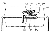
- the silicone resins 104 and 107 are completely cured to obtain a hardened structure, thereby forming an encapsulating material 108. Then, unwanted sections in the lead frame 130 are removed to form geometry as shown in Fig. 12 .
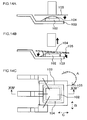
- FIG. 14A A process for installing an electrically insulating film on a lead frame in the side of a photo acceptor in the current manufacturing process for general opposed couplers will be described below.
- a soft transparent silicone resin 104 is applied over the lead frame 103 in the side of a photo acceptor, and then the electrically insulating film 105 is installed thereon.
- the electrically insulating film 105 is depressed by its self-weight, and is inclined toward various directions. Therefore, as shown in Fig. 14C , the electrically insulating film 105 may rotate along "A" direction, or may dislocate along "B" or "C” direction.
- distances D and E between the end sections of the encapsulating material 108 and the electrically insulating film 105, respectively may be extremely decreased as shown in Figs. 15A and 15B , depending upon the level of unwanted rotation or dislocation of the electrically insulating film 105.
- the electrically insulating film 105 may partially protrude beyond the encapsulating material 108, or a package-crack may be generated on thinned sections of the encapsulating material 108 (sections indicated by "distance D and E") due to a stress concentrating during the production.
- a photo coupler comprising: a first lead frame; a second lead frame having an end section bent toward the first lead frame; a first optical device, which is one of a light emitting element and a light receiving element, and is fixed to the first lead frame; a second optical device, which is the other of the light emitting element and the light receiving element and is fixed to the second lead frame so as to be opposed to the first optical device; and an electrically insulating film, provided between the first optical device and the second optical device, and including an end section having protruding and contracting sections in plan view, wherein the end section of the second lead frame has protruding and contracting sections in plan view, and wherein the end section of the electrically insulating film is fitted in the end section of the second lead frame.
- protruding and contracting sections are provided in both end sections of the electrically insulating film and the second lead frame. Further, one of the end sections fits in the other of the end sections. This allows preventing the electrically insulating film from causing an unwanted rotation or a dislocation during the manufacturing thereof.
- a method for manufacturing the photo coupler as described above comprising: fixing the first optical device and the second optical device to the first lead frame and the second lead frame, respectively; disposing the electrically insulating film on the second optical device fixed to the second lead frame, so that the end section of the electrically insulating film is fitted in the end section of the second lead frame; and fixing the first lead frame to the electrically insulating film, so that the first optical device faces the second optical device across the electrically insulating film.
- the electrically insulating film is disposed, so that the end section of the electrically insulating film is fitted in the end section of the second lead frame. This allows preventing the electrically insulating film from causing an unwanted rotation or a dislocation.
- a photo coupler which is capable of preventing the electrically insulating film from causing an unwanted rotation or a dislocation during the manufacturing thereof, and a method for manufacturing thereof, are achieved.
- Fig. 1 illustrates an embodiment of a photo coupler according to the present invention.
- Fig. 2A and Fig. 2B illustrate an electrically insulating film 5 and a lead frame 3, which are provided to the photo coupler, respectively.
- the lead frame 3 in a status of having a light receiving element 2 installed thereto is shown in Figs. 2B and 2C .
- the photo coupler includes a lead frame 6 (first lead frame), a lead frame 3 (second lead frame) having an end section 9 bent toward the lead frame 6, a light emitting element 1 (first optical device) fixed to the lead frame 6, a light receiving element 2 (second optical device) fixed to the lead frame 3 so as to face the light emitting element 1, and an electrically insulating film 5, provided between the light emitting element 1 and the light receiving element 2, and including an end section 10 having protruding and contracting sections in plan view.
- An end section 9 of the lead frame 3 has protruding and contracting sections in plan view. Further, the end section 10 of the electrically insulating film 5 fits in the end section 9 of the lead frame 3.
- the light emitting element 1 and the light receiving element 2 are, for example, a light emitting diode and a photodiode, respectively.
- An electrically insulating film 5 is fixed the light receiving element 2 and the lead frame 3 by a transparent resin 4. Further, the light emitting element 1 and the lead frame 6 are fixed to the electrically insulating film 5 by a transparent resin 7.
- the resins 4 and 7 are, for example, silicone resins. Further, an encapsulating material 8 is formed so as to cover the light emitting element 1, the light receiving element 2, the lead frame 3, the electrically insulating film 5 and the lead frame 6.
- the electrically insulating film 5 includes a base 5a (first base) and a protruding portion 5b protruding from the base 5a (first protruding portion).
- the electrically insulating film 5 further includes a protruding portion 5c (fourth protruding portion) and a protruding portion 5d (fifth protruding portion), both of which also protrude from the base 5a.
- the electrically insulating film 5 having such geometry may be obtained by a punching process with, for example, a metal mold. Therefore, a material of electrically insulating film 5 is preferably composed of a suitable material having a suitable thickness, which is transparent and is capable of being easily cut with a metal mold. Typical example of such material may be, for example, polyimide resins.
- the lead frame 3 includes a base 3a (the second base), and a protruding portion 3b (second protruding portion) and a protruding portion 3c (the third protruding portion), both of which protrude from the base 3a.
- the lead frame 3 having such geometry may be obtained by an etching process or a pressing process.
- Typical materials for the lead frame 3 may include copper, iron and the like.
- the electrically insulating film 5 is disposed on the light receiving element 2, and then, the protruding portion 5b of the electrically insulating film 5 interposes between the protruding portions 3b and 3c of lead frame 3.
- the protruding portion 3b of the lead frame 3 also interposes between the protruding portions 5b and 5c of the electrically insulating film 5.
- the protruding portion 3c of the lead frame 3 is disposed between the protruding portions 5b and 5d of the electrically insulating film 5.
- a process for manufacturing a photo coupler shown in Figs. 1A and 1B will be described as an embodiment of a process for manufacturing a photo coupler according to the present invention.
- the light emitting element 1 and the light receiving element 2 are fixed to the lead frame 6 and the lead frame 3, respectively.
- the resin 4 is applied over the light receiving element 2, and then the electrically insulating film 5 is provided on the light receiving element 2 fixed to the lead frame 3, so that the end section 10 of the electrically insulating film 5 fits in the end section 9 of the lead frame 3. Thereafter, the resin 4 is cured.
- the resin 7 is applied over the light emitting element 1, and then the lead frame 6 is fixed to the electrically insulating film 5, so that the light emitting element 1 faces the light receiving element 2 across the electrically insulating film 5. This allows forming an optical coupling of the light emitting element 1 with the light receiving element 2. Subsequently, the resins 4 and 7 are completely cured to obtain a hardened structure, thereby forming the encapsulating material 8.
- the photo coupler of Figs. 1A and 1B is here obtained, according to the above-described process.
- the protruding and the contracting sections are provided in the end section 10 of the electrically insulating film 5 and the end section 9 of the lead frame 3.
- the end section 10 fits in the end section 9. This allows preventing the electrically insulating film 5 from causing an unwanted rotation or a dislocation during the manufacture thereof. More specifically, this allows preventing the electrically insulating film 5 from rotating along "A" direction, or from dislocating along "B” or “C” direction, as shown in Fig. 3A .
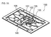
- an electrically insulating film 105 is supported by end sections 135 and 146 in the emitter-side lead frame as shown in Fig. 10 , and thus it might be considered that this configuration provides an inhibition for the rotation.
- the rotation of the electrically insulating film 105 is mainly caused during the sinking of the electrically insulating film 105 in a silicone resin 104 by its self weight. Therefore, when the level of the bending of the emission side lead frame 106 is smaller and the end sections 135 and 146 are located below a stabilized position of the electrically insulating film 105, a dislocation or a rotation may be generated.
- a rotation of the electrically insulating film 105 can be prevented by providing the emitter-side lead frame 103 having larger level of bending to form a structure, in which the end sections 135 and 146 are located above the stabile position of the electrically insulating film 105.
- the following problem may be caused.
- the end sections 135 and 146, which function as weights for pushing the electrically insulating film 105 is a portion of the lead frame 106, which is in the side opposite to the side having the electrically insulating film 105 thereon. Therefore, the photo coupler described in Japanese Patent Laid-Open No. S58-95,879 has the structure, in which the electrically insulating film 105 is inevitably in contact with both of the upper and lower lead frames 103 and 106 (see Fig. 12 ). If both of the lead frames 103 and 106 are brought into contact with the electrically insulating film 105, an internal creeping distance thereof is decreased, causing a problem of deterioration in the isolation voltage.
- the electrically insulating film 5 is supported by the lead frame 3 in the side having the electrically insulating film 5 installed thereon in the structure of the present embodiment, the other lead frame 6 is not in contact with the electrically insulating film 5. More specifically, the electrically insulating film 5 is in contact only with the lead frame 3 and not in contact with the lead frame 6. Therefore, sufficient internal creeping distance can be assured, and the unwanted rotation can be inhibited without reducing an isolation voltage. Further, according to the present embodiment, a dead space as indicated by "F" in Fig. 11 is not created, and an additional allowance of the package size in consideration of an unwanted rotation and dislocation of the electrically insulating film 5 is not required, so that photo coupler having smaller package size can be manufactured.
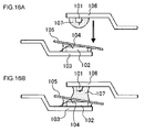
- the electrically insulating film 105 is installed, and then a silicone resin 107 is applied over the light emitting element 101, and the light emitting element 101 is superimposed over the electrically insulating film 105.
- a positional variation of the electrically insulating film 105 may lead to a variation of geometry of the silicone resin 107.
- the variation of the geometry of the silicone resin 107 may directly lead to a variation of an optical path or an internal creeping distance, and may further lead to variations of characteristics of products such as isolation voltage, receiving sensitivity or the like, eventually leading to a deterioration in the production yield of the couplers.
- the configuration of the present embodiment provides a reduced positional variation of the electrically insulating film 5, a stable geometry of the resin 7 can be achieved. Thus, variations in the isolation voltages or the receiving sensitivities can be reduced.
- the present invention is not limited to the above-described embodiments, and various modifications thereof may also be included.
- geometries of the lead frame 3 and/or the electrically insulating film 5 may be geometries shown in Fig. 5A to Fig. 7B .
- the electrically insulating film 5 is composed of the base 5a and the protruding portion 5b.
- the lead frame 3 is composed of the base 3a and the protruding portions 3b and 3c.
- the protruding portion 5b of the electrically insulating film 5 is disposed between the protruding portions 3b and 3c of the lead frame 3.
- the electrically insulating film 5 is composed of the base 5a and the protruding portion 5b.
- the lead frame 3 is composed of the base 3a and the protruding portions 3b and 3c. A distance between the protruding portions 3b and 3c is larger than the width of the base 3a.
- the protruding portion 5b of the electrically insulating film 5 is disposed between the protruding portions 3b and 3c of the lead frame 3.
- the electrically insulating film 5 is composed of the base 5a, and the protruding portion 5e (first protruding portion) and the protruding portion 5f (second protruding portion) extending from the base 5a.
- the lead frame 3 is composed of the base 3a and the protruding portion 3d (third protruding portion) protruding from the base 3a. The protruding portion 3d of the lead frame 3 is disposed between the protruding portions 5e and 5f of the electrically insulating film 5.
- the exemplary implementation having the light receiving element 2 installed over the lead frame 3 and the light emitting element 1 installed over the lead frame 6 has been illustrated in the above-described embodiment.
- the light emitting element 1 may alternatively be installed over the lead frame 3, and the light receiving element 2 may also be installed over the lead frame 6.
Landscapes
- Photo Coupler, Interrupter, Optical-To-Optical Conversion Devices (AREA)
Abstract
Description
- This application is based on Japanese patent application No.
2007-77,441 - The present invention relates to a photo coupler and a method for producing thereof.
- Photo couplers are devices that exchange signals by optics, in which an input side (emitting-side) is electrically insulated from an output side (receiving-side). Various technologies are proposed for providing an increased isolation voltage between the input side and the output side, and among these, a structure, which includes light emitting elements and light receiving elements that are disposed to be opposed to the light emitting elements and also includes an electrically insulating film disposed therebetween, are broadly adopted, since such structure provides an increased internal creeping distance between the light receiving element and the light emitting element to achieve an improved isolation voltage.
- Japanese Patent Laid-Open No.
S58-95,879 1983 S58-95,879 Fig. 8 to Fig. 13 . TheFig. 13 inclusively shows processes shown inFig. 8 to Fig. 12 . - First of all, one piece of a
lead frame 130 is prepared for installing both of thelight emitting element 101 and the light receiving element 102 (Fig. 8 ). Thelead frame 130 is composed of alead frame 106 for thelight emitting element 101 and alead frame 103 for thelight receiving element 102. Then, thelight emitting element 101 and thelight receiving element 102 are installed on an upper principal surface of thelead frame 130, and then are wired to respective lead terminals by a wire bonding process (Fig. 9 ). - Next, a smaller amount of
transparent silicone resin 104 is applied over an upper surface of thelight receiving element 102, and an electricallyinsulating film 105 is installed thereon, and then thesilicone resin 104 is cured. Subsequently, atransparent silicone resin 107 is applied over thelight emitting element 101. Thereafter, thelead frame 130 is bent at a certain location so that thelight emitting element 101 and thelight receiving element 102 are mutually opposed with the electrically insulatingfilm 105 disposed therebetween (seeFig. 10 andFig. 11 ). This achieves an optical coupling between thelight receiving element 102 and thelight emitting element 101. - Next, the
silicone resins material 108. Then, unwanted sections in thelead frame 130 are removed to form geometry as shown inFig. 12 . - A process for installing an electrically insulating film on a lead frame in the side of a photo acceptor in the current manufacturing process for general opposed couplers will be described below. First of all, as shown in
Fig. 14A , a softtransparent silicone resin 104 is applied over thelead frame 103 in the side of a photo acceptor, and then the electrically insulatingfilm 105 is installed thereon. Then, as shown inFig. 14B , the electrically insulatingfilm 105 is depressed by its self-weight, and is inclined toward various directions. Therefore, as shown inFig. 14C , the electrically insulatingfilm 105 may rotate along "A" direction, or may dislocate along "B" or "C" direction. - Then, distances D and E between the end sections of the encapsulating
material 108 and the electrically insulatingfilm 105, respectively may be extremely decreased as shown inFigs. 15A and 15B , depending upon the level of unwanted rotation or dislocation of the electrically insulatingfilm 105. This triggers a failure in the production of the photo coupler. For example, the electrically insulatingfilm 105 may partially protrude beyond the encapsulatingmaterial 108, or a package-crack may be generated on thinned sections of the encapsulating material 108 (sections indicated by "distance D and E") due to a stress concentrating during the production. - According to one aspect of the present invention, there is provided a photo coupler, comprising: a first lead frame; a second lead frame having an end section bent toward the first lead frame; a first optical device, which is one of a light emitting element and a light receiving element, and is fixed to the first lead frame; a second optical device, which is the other of the light emitting element and the light receiving element and is fixed to the second lead frame so as to be opposed to the first optical device; and an electrically insulating film, provided between the first optical device and the second optical device, and including an end section having protruding and contracting sections in plan view, wherein the end section of the second lead frame has protruding and contracting sections in plan view, and wherein the end section of the electrically insulating film is fitted in the end section of the second lead frame.
- In this photo coupler, protruding and contracting sections are provided in both end sections of the electrically insulating film and the second lead frame. Further, one of the end sections fits in the other of the end sections. This allows preventing the electrically insulating film from causing an unwanted rotation or a dislocation during the manufacturing thereof.
- According to another aspect of the present invention, there is provided a method for manufacturing the photo coupler as described above, comprising: fixing the first optical device and the second optical device to the first lead frame and the second lead frame, respectively; disposing the electrically insulating film on the second optical device fixed to the second lead frame, so that the end section of the electrically insulating film is fitted in the end section of the second lead frame; and fixing the first lead frame to the electrically insulating film, so that the first optical device faces the second optical device across the electrically insulating film.
- In such manufacturing method, the electrically insulating film is disposed, so that the end section of the electrically insulating film is fitted in the end section of the second lead frame. This allows preventing the electrically insulating film from causing an unwanted rotation or a dislocation.
- According to the present invention, a photo coupler, which is capable of preventing the electrically insulating film from causing an unwanted rotation or a dislocation during the manufacturing thereof, and a method for manufacturing thereof, are achieved.
- The above and other objects, advantages and features of the present invention will be more apparent from the following description of certain preferred embodiments taken in conjunction with the accompanying drawings, in which:
-
Fig. 1A is a schematic plan view, illustrating an embodiment of a photo coupler according to the present invention; -
Fig. 1B is a cross-sectional view, illustrating an embodiment of a photo coupler according to the present invention; -
Fig. 2A is a diagram, illustrating an electrically insulating film provided in a photo coupler ofFig. 1 ; -
Fig. 2B is a schematic plan view, illustrating a second lead frame; -
Fig. 2C is a cross-sectional view, illustrating a second lead frame; -
Fig. 3A is a schematic plan view, illustrating a structure after disposing an electrically insulating film; -
Fig. 3B is a cross-sectional view, illustrating a structure after disposing an electrically insulating film; -
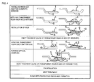
Fig. 4 is a diagram, useful in describing an embodiment of the process for manufacturing the photo coupler according to the present invention; -
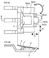
Fig. 5A is a schematic plan view, illustrating a modified embodiment according to the present invention; -
Fig. 5B is a cross-sectional view, illustrating a modified embodiment according to the present invention; -
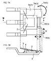
Fig. 6A is a schematic plan view, illustrating a modified embodiment according to the present invention; -
Fig. 6B is a cross-sectional view, illustrating a modified embodiment according to the present invention; -
Fig. 7A is a schematic plan view, illustrating a modified embodiment according to the present invention; -
Fig. 7B is a cross-sectional view, illustrating a modified embodiment according to the present invention; -
Fig. 8 is a diagram, useful in describing an embodiment of the process for manufacturing the photo coupler according to the conventional photo coupler; -
Fig. 9 is a diagram, useful in describing an embodiment of the process for manufacturing the photo coupler according to the conventional photo coupler; -
Fig. 10 is a diagram, useful in describing an embodiment of the process for manufacturing the photo coupler according to the conventional photo coupler; -
Fig. 11 is a diagram, useful in describing an embodiment of the process for manufacturing the photo coupler according to the conventional photo coupler; -
Fig. 12 is a diagram, useful in describing an embodiment of the process for manufacturing the photo coupler according to the conventional photo coupler; -
Fig. 13 is a diagram, useful in describing an embodiment of the process for manufacturing the photo coupler according to the conventional photo coupler; -
Figs. 14A to 14C are diagrams, useful in describing a problem in the process for manufacturing the photo coupler according to the conventional photo coupler; -
Fig. 15A is a schematic plan view, useful in describing a problem in the process for manufacturing the photo coupler according to the conventional photo coupler; -
Fig. 15B is a cross-sectional view, useful in describing a problem in the process for manufacturing the photo coupler according to the conventional photo coupler; and -
Figs. 16A to 16B are diagrams, useful in describing a problem in the process for manufacturing the photo coupler according to the conventional photo coupler. - The invention will be now described herein with reference to illustrative embodiments. Those skilled in the art will recognize that many alternative embodiments can be accomplished using the teachings of the present invention and that the invention is not limited to the embodiments illustrated for explanatory purposed.
- Exemplary implementations according to the present invention will be described in reference to the annexed figures. In all figures, an identical numeral is assigned to an element commonly appeared in the figures, and the detailed description thereof will not be repeated.
-
Fig. 1 illustrates an embodiment of a photo coupler according to the present invention.Fig. 2A and Fig. 2B illustrate an electrically insulatingfilm 5 and alead frame 3, which are provided to the photo coupler, respectively. Thelead frame 3 in a status of having alight receiving element 2 installed thereto is shown inFigs. 2B and 2C . - The photo coupler includes a lead frame 6 (first lead frame), a lead frame 3 (second lead frame) having an
end section 9 bent toward thelead frame 6, a light emitting element 1 (first optical device) fixed to thelead frame 6, a light receiving element 2 (second optical device) fixed to thelead frame 3 so as to face thelight emitting element 1, and an electrically insulatingfilm 5, provided between the light emittingelement 1 and thelight receiving element 2, and including anend section 10 having protruding and contracting sections in plan view. Anend section 9 of thelead frame 3 has protruding and contracting sections in plan view. Further, theend section 10 of the electrically insulatingfilm 5 fits in theend section 9 of thelead frame 3. Thelight emitting element 1 and thelight receiving element 2 are, for example, a light emitting diode and a photodiode, respectively. An electrically insulatingfilm 5 is fixed thelight receiving element 2 and thelead frame 3 by atransparent resin 4. Further, thelight emitting element 1 and thelead frame 6 are fixed to the electrically insulatingfilm 5 by a transparent resin 7. Theresins 4 and 7 are, for example, silicone resins. Further, an encapsulatingmaterial 8 is formed so as to cover thelight emitting element 1, thelight receiving element 2, thelead frame 3, the electrically insulatingfilm 5 and thelead frame 6. - As shown in
Fig. 2A , the electrically insulatingfilm 5 includes abase 5a (first base) and a protrudingportion 5b protruding from thebase 5a (first protruding portion). The electrically insulatingfilm 5 further includes a protrudingportion 5c (fourth protruding portion) and a protrudingportion 5d (fifth protruding portion), both of which also protrude from thebase 5a. The electrically insulatingfilm 5 having such geometry may be obtained by a punching process with, for example, a metal mold. Therefore, a material of electrically insulatingfilm 5 is preferably composed of a suitable material having a suitable thickness, which is transparent and is capable of being easily cut with a metal mold. Typical example of such material may be, for example, polyimide resins. - On the other hand, as shown in
Figs. 2B and 2C , thelead frame 3 includes abase 3a (the second base), and a protrudingportion 3b (second protruding portion) and a protrudingportion 3c (the third protruding portion), both of which protrude from thebase 3a. Thelead frame 3 having such geometry may be obtained by an etching process or a pressing process. Typical materials for thelead frame 3 may include copper, iron and the like. - As shown in
Figs. 3A and 3B , the electrically insulatingfilm 5 is disposed on thelight receiving element 2, and then, the protrudingportion 5b of the electrically insulatingfilm 5 interposes between the protrudingportions lead frame 3. The protrudingportion 3b of thelead frame 3 also interposes between the protrudingportions film 5. Similarly, the protrudingportion 3c of thelead frame 3 is disposed between the protrudingportions film 5. - In reference to
Fig. 4 , an exemplary implementation of a process for manufacturing a photo coupler shown inFigs. 1A and 1B will be described as an embodiment of a process for manufacturing a photo coupler according to the present invention. First of all, thelight emitting element 1 and thelight receiving element 2 are fixed to thelead frame 6 and thelead frame 3, respectively. Subsequently, theresin 4 is applied over thelight receiving element 2, and then the electrically insulatingfilm 5 is provided on thelight receiving element 2 fixed to thelead frame 3, so that theend section 10 of the electrically insulatingfilm 5 fits in theend section 9 of thelead frame 3. Thereafter, theresin 4 is cured. - Next, the resin 7 is applied over the
light emitting element 1, and then thelead frame 6 is fixed to the electrically insulatingfilm 5, so that thelight emitting element 1 faces thelight receiving element 2 across the electrically insulatingfilm 5. This allows forming an optical coupling of thelight emitting element 1 with thelight receiving element 2. Subsequently, theresins 4 and 7 are completely cured to obtain a hardened structure, thereby forming the encapsulatingmaterial 8. The photo coupler ofFigs. 1A and 1B is here obtained, according to the above-described process. - Advantageous effects of the present embodiment will be described. In the present embodiment, the protruding and the contracting sections are provided in the
end section 10 of the electrically insulatingfilm 5 and theend section 9 of thelead frame 3. Theend section 10 fits in theend section 9. This allows preventing the electrically insulatingfilm 5 from causing an unwanted rotation or a dislocation during the manufacture thereof. More specifically, this allows preventing the electrically insulatingfilm 5 from rotating along "A" direction, or from dislocating along "B" or "C" direction, as shown inFig. 3A . - Meanwhile, in the case of the process for manufacturing the photo coupler described in Japanese Patent Laid-Open No.
S58-95,879 film 105 is supported byend sections Fig. 10 , and thus it might be considered that this configuration provides an inhibition for the rotation. However, the rotation of the electrically insulatingfilm 105 is mainly caused during the sinking of the electrically insulatingfilm 105 in asilicone resin 104 by its self weight. Therefore, when the level of the bending of the emissionside lead frame 106 is smaller and theend sections film 105, a dislocation or a rotation may be generated. - Needless to add, a rotation of the electrically insulating
film 105 can be prevented by providing the emitter-side lead frame 103 having larger level of bending to form a structure, in which theend sections film 105. However, in such case, the following problem may be caused. - The
end sections film 105 is a portion of thelead frame 106, which is in the side opposite to the side having the electrically insulatingfilm 105 thereon. Therefore, the photo coupler described in Japanese Patent Laid-Open No.S58-95,879 film 105 is inevitably in contact with both of the upper and lower lead frames 103 and 106 (seeFig. 12 ). If both of the lead frames 103 and 106 are brought into contact with the electrically insulatingfilm 105, an internal creeping distance thereof is decreased, causing a problem of deterioration in the isolation voltage. Thus, it is not preferable to have a structure, in which the electrically insulatingfilm 105 is supported by thelead frame 106 that is in the side opposite to the side having the electrically insulatingfilm 105 thereon. Further, if the emitter-side lead frame 106 is bent, an additional space as indicated by "F" inFig. 11 may be created, and thus this causes a difficulty in the downsizing of the device. - On the contrary, since the electrically insulating
film 5 is supported by thelead frame 3 in the side having the electrically insulatingfilm 5 installed thereon in the structure of the present embodiment, theother lead frame 6 is not in contact with the electrically insulatingfilm 5. More specifically, the electrically insulatingfilm 5 is in contact only with thelead frame 3 and not in contact with thelead frame 6. Therefore, sufficient internal creeping distance can be assured, and the unwanted rotation can be inhibited without reducing an isolation voltage. Further, according to the present embodiment, a dead space as indicated by "F" inFig. 11 is not created, and an additional allowance of the package size in consideration of an unwanted rotation and dislocation of the electrically insulatingfilm 5 is not required, so that photo coupler having smaller package size can be manufactured. - Further, in a general process for manufacturing photo couplers, as shown in
Fig. 16A and Fig. 16B , the electrically insulatingfilm 105 is installed, and then asilicone resin 107 is applied over thelight emitting element 101, and thelight emitting element 101 is superimposed over the electrically insulatingfilm 105. A positional variation of the electrically insulatingfilm 105 may lead to a variation of geometry of thesilicone resin 107. Then, the variation of the geometry of thesilicone resin 107 may directly lead to a variation of an optical path or an internal creeping distance, and may further lead to variations of characteristics of products such as isolation voltage, receiving sensitivity or the like, eventually leading to a deterioration in the production yield of the couplers. - On the contrary, since the configuration of the present embodiment provides a reduced positional variation of the electrically insulating
film 5, a stable geometry of the resin 7 can be achieved. Thus, variations in the isolation voltages or the receiving sensitivities can be reduced. - The present invention is not limited to the above-described embodiments, and various modifications thereof may also be included. For example, geometries of the
lead frame 3 and/or the electrically insulatingfilm 5 may be geometries shown inFig. 5A to Fig. 7B . InFigs. 5A and 5B , the electrically insulatingfilm 5 is composed of thebase 5a and the protrudingportion 5b. Further, thelead frame 3 is composed of thebase 3a and the protrudingportions portion 5b of the electrically insulatingfilm 5 is disposed between the protrudingportions lead frame 3. - In
Figs. 6A and 6B , the electrically insulatingfilm 5 is composed of thebase 5a and the protrudingportion 5b. Further, thelead frame 3 is composed of thebase 3a and the protrudingportions portions base 3a. The protrudingportion 5b of the electrically insulatingfilm 5 is disposed between the protrudingportions lead frame 3. - In
Figs. 7A and 7B , the electrically insulatingfilm 5 is composed of thebase 5a, and the protrudingportion 5e (first protruding portion) and the protrudingportion 5f (second protruding portion) extending from thebase 5a. Further, thelead frame 3 is composed of thebase 3a and the protrudingportion 3d (third protruding portion) protruding from thebase 3a. The protrudingportion 3d of thelead frame 3 is disposed between the protrudingportions film 5. - The exemplary implementation having the
light receiving element 2 installed over thelead frame 3 and thelight emitting element 1 installed over thelead frame 6 has been illustrated in the above-described embodiment. However, thelight emitting element 1 may alternatively be installed over thelead frame 3, and thelight receiving element 2 may also be installed over thelead frame 6. - It is apparent that the present invention is not limited to the above embodiment, and may be modified and changed without departing from the scope and spirit of the invention.
Claims (7)
- A photo coupler, comprising:a first lead frame;a second lead frame having an end section bent toward said first lead frame;a first optical device, which is one of a light emitting element and a light receiving element, and is fixed to said first lead frame;a second optical device, which is the other of said light emitting element and said light receiving element and is fixed to said second lead frame so as to be opposed to said first optical device; andan electrically insulating film, provided between said first optical device and said second optical device, and including an end section having protruding and contracting sections in plan view,wherein said end section of said second lead frame has protruding and contracting sections in plan view, and
wherein said end section of said electrically insulating film is fitted in said end section of said second lead frame. - The photo coupler as set forth in claim 1,
wherein said electrically insulating film is in contact with only said second lead frame and not in contact with said first lead frame. - The photo coupler as set forth in claim 1 ,
wherein said electrically insulating film includes a first base and a first protruding portion protruding from said first base,
wherein said second lead frame includes a second base, and a second protruding portion and a third protruding portion protruding from said second base, and
wherein said first protruding portion of said electrically insulating film is disposed between said second and said third protruding portions of said second lead frame. - The photo coupler as set forth in claim 3,
wherein said electrically insulating film includes a fourth protruding portion and a fifth protruding portion, both of which protrude from said first base,
said second protruding portion of said second lead frame is disposed between said first protruding portion and said fourth protruding portion of said electrically insulating film, and
wherein said third protruding portion of said second lead frame is disposed between said first protruding portion and said fifth protruding portion of said electrically insulating film. - The photo coupler as set forth in claim 3,
wherein a distance between said second protruding portion and said third protruding portion of said second lead frame is larger than a width of said second base. - The photo coupler as set forth in claim 1,
wherein said electrically insulating film includes a first base, and a first protruding portion and a second protruding portion protruding from said first base,
wherein said second lead frame includes a second base, and a third protruding portion protruding from said second base, and
wherein said third protruding portion of said second lead frame is disposed between said first protruding portion and said second protruding portion of said electrically insulating film. - A method for manufacturing the photo coupler as set forth in claim 1, comprising:fixing said first optical device and said second optical device to said first lead frame and said second lead frame, respectively;disposing said electrically insulating film over said second optical device fixed to said second lead frame, so that said end section of said electrically insulating film is fitted in said end section of said second lead frame; andfixing said first lead frame to said electrically insulating film, so that said first optical device faces said second optical device across said electrically insulating film.
Applications Claiming Priority (1)
| Application Number | Priority Date | Filing Date | Title |
|---|---|---|---|
| JP2007077441A JP4897530B2 (en) | 2007-03-23 | 2007-03-23 | Photocoupler and its assembly method |
Publications (3)
| Publication Number | Publication Date |
|---|---|
| EP1973172A2 true EP1973172A2 (en) | 2008-09-24 |
| EP1973172A3 EP1973172A3 (en) | 2011-07-20 |
| EP1973172B1 EP1973172B1 (en) | 2013-05-08 |
Family
ID=39618910
Family Applications (1)
| Application Number | Title | Priority Date | Filing Date |
|---|---|---|---|
| EP08005170.9A Expired - Fee Related EP1973172B1 (en) | 2007-03-23 | 2008-03-19 | Photo coupler and method for producing same |
Country Status (3)
| Country | Link |
|---|---|
| US (1) | US7488964B2 (en) |
| EP (1) | EP1973172B1 (en) |
| JP (1) | JP4897530B2 (en) |
Families Citing this family (5)
| Publication number | Priority date | Publication date | Assignee | Title |
|---|---|---|---|---|
| US9029818B2 (en) | 2012-06-21 | 2015-05-12 | Avago Technologies General Ip (Singapore) Pte. Ltd. | Optoelectronic device and method of manufacture |
| US8853658B2 (en) | 2012-08-08 | 2014-10-07 | Avago Technologies General Ip (Singapore) Pte. Ltd. | Face-to-face opto-coupler device and method of manufacture |
| JP5865216B2 (en) * | 2012-09-12 | 2016-02-17 | ルネサスエレクトロニクス株式会社 | Photo coupler |
| JP6345532B2 (en) * | 2014-08-07 | 2018-06-20 | ルネサスエレクトロニクス株式会社 | Optical coupling device manufacturing method, optical coupling device, and power conversion system |
| US10283699B2 (en) * | 2016-01-29 | 2019-05-07 | Avago Technologies International Sales Pte. Limited | Hall-effect sensor isolator |
Citations (1)
| Publication number | Priority date | Publication date | Assignee | Title |
|---|---|---|---|---|
| JPS5895879A (en) | 1981-10-14 | 1983-06-07 | ゼネラル・エレクトリツク・カンパニイ | Bendable lead frame and optocoupler |
Family Cites Families (21)
| Publication number | Priority date | Publication date | Assignee | Title |
|---|---|---|---|---|
| GB1557685A (en) * | 1976-02-02 | 1979-12-12 | Fairchild Camera Instr Co | Optically coupled isolator device |
| JPS5339894A (en) * | 1976-09-24 | 1978-04-12 | Nec Corp | Photo coupling isolator |
| JPS57166357A (en) * | 1981-04-01 | 1982-10-13 | Kyowa Giken | Manufacture of fiber reinforced slag gypsum composite material |
| JPS58162080A (en) * | 1982-03-19 | 1983-09-26 | Nec Corp | optical coupling device |
| JPS61151355A (en) * | 1984-12-25 | 1986-07-10 | 株式会社 栗本鉄工所 | Hollow slab |
| JPS61228681A (en) * | 1985-04-01 | 1986-10-11 | Sharp Corp | Light coupling semiconductor device |
| JPS61292974A (en) * | 1985-06-20 | 1986-12-23 | Sharp Corp | Photo-coupler |
| US4863806A (en) * | 1985-06-25 | 1989-09-05 | Hewlett-Packard Company | Optical isolator |
| US4694183A (en) * | 1985-06-25 | 1987-09-15 | Hewlett-Packard Company | Optical isolator fabricated upon a lead frame |
| US5148243A (en) * | 1985-06-25 | 1992-09-15 | Hewlett-Packard Company | Optical isolator with encapsulation |
| US4857407A (en) * | 1987-06-16 | 1989-08-15 | Ppg Industries, Inc. | Low modulus interlayer |
| JPS6416649U (en) * | 1987-07-20 | 1989-01-27 | ||
| JPH01128478A (en) * | 1987-11-12 | 1989-05-22 | Mitsubishi Electric Corp | Semiconductor photocoupler device |
| US4980568A (en) * | 1989-05-22 | 1990-12-25 | Hewlett-Packard Company | Optical isolator having high voltage isolation and high light flux light guide |
| JPH05327004A (en) * | 1992-04-01 | 1993-12-10 | Nec Corp | Semiconductor photocoupler |
| US5389578A (en) * | 1994-01-04 | 1995-02-14 | Texas Instruments Incorporated | Optical coupler |
| JP2600616B2 (en) * | 1994-09-08 | 1997-04-16 | 日本電気株式会社 | Optical coupling device |
| JP3416697B2 (en) * | 1996-04-22 | 2003-06-16 | シャープ株式会社 | Optical coupling device |
| JP2003282935A (en) * | 2002-03-26 | 2003-10-03 | Sharp Corp | Optical coupling element, method for manufacturing the same, and electronic device |
| JP4205412B2 (en) * | 2002-12-02 | 2009-01-07 | Necエンジニアリング株式会社 | Method for manufacturing optically coupled semiconductor device |
| JP2005159137A (en) * | 2003-11-27 | 2005-06-16 | Sharp Corp | Optical semiconductor element and electronic apparatus using the optical semiconductor element |
-
2007
- 2007-03-23 JP JP2007077441A patent/JP4897530B2/en not_active Expired - Fee Related
-
2008
- 2008-03-13 US US12/047,758 patent/US7488964B2/en not_active Expired - Fee Related
- 2008-03-19 EP EP08005170.9A patent/EP1973172B1/en not_active Expired - Fee Related
Patent Citations (1)
| Publication number | Priority date | Publication date | Assignee | Title |
|---|---|---|---|---|
| JPS5895879A (en) | 1981-10-14 | 1983-06-07 | ゼネラル・エレクトリツク・カンパニイ | Bendable lead frame and optocoupler |
Also Published As
| Publication number | Publication date |
|---|---|
| EP1973172B1 (en) | 2013-05-08 |
| EP1973172A3 (en) | 2011-07-20 |
| JP4897530B2 (en) | 2012-03-14 |
| US20080230727A1 (en) | 2008-09-25 |
| JP2008235831A (en) | 2008-10-02 |
| US7488964B2 (en) | 2009-02-10 |
Similar Documents
| Publication | Publication Date | Title |
|---|---|---|
| CN101218673B (en) | Semiconductor device | |
| EP1973172B1 (en) | Photo coupler and method for producing same | |
| US6603148B1 (en) | Semiconductor device | |
| JP5004601B2 (en) | Package component manufacturing method and semiconductor device manufacturing method | |
| US20070235845A1 (en) | Apparatus, system and method for use in mounting electronic elements | |
| US10036666B2 (en) | Photosensor including sensor circuit assembly with light emitter and receiver that face each other | |
| JP2005079537A (en) | Solid-state imaging device and manufacturing method thereof | |
| JP2011049244A (en) | Resin-sealed semiconductor device | |
| JP2010153861A (en) | Light emitting diode package structure | |
| US7170099B2 (en) | Optical semiconductor device and a method for manufacturing the same | |
| JP2006108306A (en) | Lead frame and semiconductor package using the same | |
| CN215680663U (en) | Semiconductor device with a plurality of semiconductor chips | |
| US8024972B2 (en) | Electronic part, method for fabricating electronic part, acceleration sensor, and method for fabricating acceleration sensor | |
| US6097084A (en) | Photointerruptor | |
| JP3274126B2 (en) | Connector type semiconductor device | |
| US10243107B2 (en) | Light emitting device and method for manufacturing thereof | |
| CN102694294B (en) | Connector easily enabling a reduction in thickness and being structurally stable | |
| JP2010153816A (en) | Photo coupler and its assembling method | |
| CN1316637C (en) | Semiconductor device | |
| CN113496956B (en) | Semiconductor device and method for manufacturing semiconductor device | |
| JP4759314B2 (en) | Solid-state imaging device manufacturing method and solid-state imaging device | |
| JP2006332685A (en) | Solid-state imaging device | |
| JP4172782B2 (en) | Optical semiconductor element storage package and optical semiconductor device | |
| JP2005049208A (en) | Acceleration sensor and method of manufacturing the same | |
| CN111656540A (en) | semiconductor device |
Legal Events
| Date | Code | Title | Description |
|---|---|---|---|
| PUAI | Public reference made under article 153(3) epc to a published international application that has entered the european phase |
Free format text: ORIGINAL CODE: 0009012 |
|
| AK | Designated contracting states |
Kind code of ref document: A2 Designated state(s): AT BE BG CH CY CZ DE DK EE ES FI FR GB GR HR HU IE IS IT LI LT LU LV MC MT NL NO PL PT RO SE SI SK TR |
|
| AX | Request for extension of the european patent |
Extension state: AL BA MK RS |
|
| RAP1 | Party data changed (applicant data changed or rights of an application transferred) |
Owner name: RENESAS ELECTRONICS CORPORATION |
|
| PUAL | Search report despatched |
Free format text: ORIGINAL CODE: 0009013 |
|
| AK | Designated contracting states |
Kind code of ref document: A3 Designated state(s): AT BE BG CH CY CZ DE DK EE ES FI FR GB GR HR HU IE IS IT LI LT LU LV MC MT NL NO PL PT RO SE SI SK TR |
|
| AX | Request for extension of the european patent |
Extension state: AL BA MK RS |
|
| 17P | Request for examination filed |
Effective date: 20111215 |
|
| 17Q | First examination report despatched |
Effective date: 20120210 |
|
| AKX | Designation fees paid |
Designated state(s): DE |
|
| REG | Reference to a national code |
Ref country code: DE Ref legal event code: R079 Ref document number: 602008024371 Country of ref document: DE Free format text: PREVIOUS MAIN CLASS: H01L0031120000 Ipc: H01L0031167000 |
|
| GRAP | Despatch of communication of intention to grant a patent |
Free format text: ORIGINAL CODE: EPIDOSNIGR1 |
|
| RIC1 | Information provided on ipc code assigned before grant |
Ipc: H01L 31/0203 20060101ALI20121016BHEP Ipc: H01L 31/12 20060101ALI20121016BHEP Ipc: H01L 31/167 20060101AFI20121016BHEP |
|
| GRAS | Grant fee paid |
Free format text: ORIGINAL CODE: EPIDOSNIGR3 |
|
| GRAA | (expected) grant |
Free format text: ORIGINAL CODE: 0009210 |
|
| AK | Designated contracting states |
Kind code of ref document: B1 Designated state(s): DE |
|
| REG | Reference to a national code |
Ref country code: DE Ref legal event code: R096 Ref document number: 602008024371 Country of ref document: DE Effective date: 20130704 |
|
| PLBE | No opposition filed within time limit |
Free format text: ORIGINAL CODE: 0009261 |
|
| STAA | Information on the status of an ep patent application or granted ep patent |
Free format text: STATUS: NO OPPOSITION FILED WITHIN TIME LIMIT |
|
| 26N | No opposition filed |
Effective date: 20140211 |
|
| REG | Reference to a national code |
Ref country code: DE Ref legal event code: R097 Ref document number: 602008024371 Country of ref document: DE Effective date: 20140211 |
|
| REG | Reference to a national code |
Ref country code: DE Ref legal event code: R119 Ref document number: 602008024371 Country of ref document: DE |
|
| REG | Reference to a national code |
Ref country code: DE Ref legal event code: R119 Ref document number: 602008024371 Country of ref document: DE Effective date: 20141001 |
|
| PG25 | Lapsed in a contracting state [announced via postgrant information from national office to epo] |
Ref country code: DE Free format text: LAPSE BECAUSE OF NON-PAYMENT OF DUE FEES Effective date: 20141001 |