EP1970992A1 - Superconducting disk resonator - Google Patents
Superconducting disk resonator Download PDFInfo
- Publication number
- EP1970992A1 EP1970992A1 EP08102050A EP08102050A EP1970992A1 EP 1970992 A1 EP1970992 A1 EP 1970992A1 EP 08102050 A EP08102050 A EP 08102050A EP 08102050 A EP08102050 A EP 08102050A EP 1970992 A1 EP1970992 A1 EP 1970992A1
- Authority
- EP
- European Patent Office
- Prior art keywords
- superconducting
- resonator
- dielectric
- base substrate
- signal input
- Prior art date
- Legal status (The legal status is an assumption and is not a legal conclusion. Google has not performed a legal analysis and makes no representation as to the accuracy of the status listed.)
- Withdrawn
Links
Images




Classifications
-
- H—ELECTRICITY
- H01—ELECTRIC ELEMENTS
- H01P—WAVEGUIDES; RESONATORS, LINES, OR OTHER DEVICES OF THE WAVEGUIDE TYPE
- H01P7/00—Resonators of the waveguide type
- H01P7/10—Dielectric resonators
-
- H—ELECTRICITY
- H01—ELECTRIC ELEMENTS
- H01P—WAVEGUIDES; RESONATORS, LINES, OR OTHER DEVICES OF THE WAVEGUIDE TYPE
- H01P7/00—Resonators of the waveguide type
- H01P7/08—Strip line resonators
-
- H—ELECTRICITY
- H10—SEMICONDUCTOR DEVICES; ELECTRIC SOLID-STATE DEVICES NOT OTHERWISE PROVIDED FOR
- H10N—ELECTRIC SOLID-STATE DEVICES NOT OTHERWISE PROVIDED FOR
- H10N60/00—Superconducting devices
Definitions
- the present invention relates to a superconducting disk resonator that is used in a transmitting front end such as a transmitting filter or antenna in the field of mobile communication and broadcasting.
- a superconductor is favorably considered for application to a filter of a base station of a mobile communication system since it has relatively low surface resistance even in a high frequency domain compared to a conventional electrical conductor so that a low-loss high-Q value resonator may be realized.
- a superconducting filter as a receiving side band filter
- transmission loss may be reduced and accurate frequency blocking characteristics may be realized, for example.
- distortions created by a high power amplifier may be removed, for example.
- high power is needed to transmit high frequency signals and obstacles are created with respect to realizing power efficiency.
- techniques are in demand for realizing both miniaturization and efficient power consumption in a transmitting side band filter.
- a microstrip line pattern such as a hairpin line pattern or a straight line pattern is conventionally used as a resonator pattern.
- loss may be increased. This is due to the fact that high frequency waves such as microwaves are prone to concentrate at edge portions of a conductor which causes electric currents to concentrate at edge or corner portions of the microstrip line pattern so that the current concentration at these portions may exceed the critical current concentration of the superconductor.
- a superconducting resonator having a disk resonator pattern as is shown in FIG. 1A has been proposed in the prior art in order to reduce current concentration at the edge portions of the resonator pattern.
- the illustrated superconducting disk resonator has a disk type superconducting resonator pattern (signal layer) 12 having fewer corner portions and edge portions formed on the surface of a dielectric base substrate 111 to realize high power response as a transmitting side filter.
- the illustrated superconducting disk resonator further includes signal input/output lines (feeders) 13 extending toward the vicinity of the superconducting resonator pattern 12 and a superconducting film 14 as a ground layer formed on the rear face of the dielectric base substrate 111.
- signal input/output lines (feeders) 13 extending toward the vicinity of the superconducting resonator pattern 12 and a superconducting film 14 as a ground layer formed on the rear face of the dielectric base substrate 111.
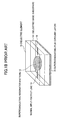
- a technique has been proposed in the prior art that involves laminating a dielectric element (or magnetic element) 15 on the disk type superconducting resonator pattern 12 as is shown in FIG. 1B in order to prevent current concentration at the peripheral portions (i.e., circumferential edge portions) of the disk type superconducting resonator pattern 12 (e.g., see Japanese Laid-Open Patent Publication No. 2006-352459 ).
- a notch occurs on the resonance curve of the resonator.
- a base substrate on which the superconducting resonator pattern is to be formed or a laminating element having dielectric or magnetic anisotropy e.g., sapphire substrate
- a notch 19 occurs on the resonance curve as is shown in FIG. 2B .
- a notch may not occur in a corresponding electromagnetic simulation and a normal resonance curve may be indicated.
- a notch may occur at the high frequency side of the resonance curve. Such a notch occurring on the resonance curve may affect filtering properties and degrade device reliability, for example.
- An aspect of the present invention is directed to providing a superconducting disk resonator that is capable of preventing occurrence of a notch on a resonance curve and maintaining suitable frequency characteristics even when an anisotropic substrate is used.
- Another aspect of the present invention is directed to providing a filter using such a superconducting disk resonator.
- a superconducting disk resonator that includes:
- a superconducting disk resonator that includes:
- a superconducting filter that includes a superconducting disk resonator according to an embodiment of the present invention.
- FIG. 3A is a plan view and FIG. 3B is a perspective view of a superconducting disk resonator 10 according to an embodiment of the present invention.
- FIG. 3C is a diagram showing frequency characteristics of the superconducting resonator 10 of FIGS. 3A and 3B .
- the illustrated superconducting disk resonator 10 includes an anisotropic dielectric base substrate 21, a disk type resonator pattern (signal layer) 12 that is made of superconducting material and is formed on the dielectric base substrate 21, a pair of signal input/output lines 13 extending in a straight line towards the superconducting resonator pattern 12.
- the superconducting disk resonator 10 also has a superconducting film (ground layer) 14 arranged on the rear face of the dielectric base substrate 21.
- YBCO (Y-Ba-Cu-O) material may be used as the superconducting material of the resonator pattern 12, the signal input/output lines 13, and the ground layer 14.
- the dielectric base substrate 21 has dielectric anisotropy in directions ⁇ 90 degrees with respect to the extending direction of the signal input/output lines 13.
- the direction of dielectric anisotropy of a dielectric substrate that is to become the base substrate is determined beforehand, and the determined anisotropic direction may be marked at an edge portion of the substrate, for example.
- superconducting films are arranged on the surface and rear face of the dielectric substrate, and a patterning process is performed on the surface of the dielectric substrate to form a disk type resonator pattern 12 and a pair of signal input/output lines 13 in each of plural resonator areas provided on the dielectric substrate.
- a patterning process appropriate measures are taken such that the extending direction of the signal input/output lines 13 forms a 90-degree angle with respect to the direction of dielectric anisotropy of the dielectric substrate.
- the dielectric substrate is cut into plural resonator areas to thereby fabricate superconducting disk resonators in each of these resonator areas.
- frequency characteristics of the superconducting disk resonator 10 may be free of notches as is shown in FIG. 3C .
- FIGS. 4A and 4B are graphs respectively showing electromagnetic simulation results and actual measurement results of a superconducting disk resonator that uses a LaAlO 3 substrate (anisotropic dielectric substrate) with dimensions of 20 mm ⁇ 20 mm ⁇ 0.5 mm, which LaAlO 3 substrate has a YBCO disk resonator pattern with a diameter of 11 mm and signal input/output lines formed on one side, and a ground layer formed on the other side.
- normal resonance curves are plotted for both S11 and S21.
- FIG. 4B in actual measurement, notches occur at the high frequency side of both of the resonance curves of S11 and S21.
- the inventors of the present invention have investigated the causes of such notch occurrence and have considered the fact that (1) a notch does not occur even in actual measurement results when an isotropic dielectric base substrate is used and a laminating element is not arranged on the superconducting disk resonator pattern but (2) even when an isotropic dielectric base substrate is used, a notch may occur in some cases when a laminating element having dielectric anisotropy or magnetic anisotropy is arranged on the superconducting resonator pattern, depending on the direction of anisotropy of the laminating element. Based on the above fact, the inventors of the present invention have come to believe that the direction of anisotropy has an influence on the occurrence of a notch. Accordingly, the following electromagnetic simulations were conducted with respect to superconducting disk resonator layouts arranged to realize dielectric anisotropy equivalent properties.
- FIG. 5A is a diagram showing a layout of a superconducting disk resonator that uses a substantially isotropic MgO base substrate 11 with dimensions of 20 mm ⁇ 20 mm ⁇ 0.5 mm.
- the MgO base substrate 11 has a YBCO disk resonator pattern 12 with a diameter of 11 mm and a pair of signal input/output lines 13 formed thereon.
- the isotropic MgO base substrate 11 further has stubs 22 with dimensions of 0.2 mm ⁇ 0.2 mm arranged thereon in directions ⁇ 45 degrees with respect to the extending direction of the signal lines 13 to realize dielectric anisotropy equivalent properties in the corresponding directions.
- FIG. 1 is a diagram showing a layout of a superconducting disk resonator that uses a substantially isotropic MgO base substrate 11 with dimensions of 20 mm ⁇ 20 mm ⁇ 0.5 mm.
- the MgO base substrate 11 has a YBCO disk resonator pattern 12
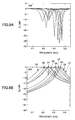
- FIG. 5B is a graph showing electromagnetic simulation results obtained with respect to the superconducting disk resonator layout shown in FIG. 5A . As is shown in FIG. 5B , notches 19 occur at the high frequency side of the resonance curves of both S11 and S21.
- FIG. 6A shows a layout equivalent to a resonator that uses a base substrate having dielectric anisotropy in directions ⁇ 90 degrees with respect to the extending direction of the signal input/output lines 13.
- the illustrated layout of FIG. 6A has stubs 22 with dimensions of 0.2 mm ⁇
- FIG. 6B is a graph showing electromagnetic simulation results of the layout shown in FIG. 6A . As is shown in this graph, notches do not occur on the resonance curves of S11 and S21 in this case.
- a substrate having no dielectric anisotropy or magnetic anisotropy is preferably used, or a substrate having dielectric or magnetic anisotropy in directions ⁇ 90 degrees with respect to the extending direction of signal input/output lines is preferably used.
- FIGS. 7A and 7B are diagrams describing a dielectric anisotropy evaluating method for confirming the above simulation results through actual measurement.
- FIG. 7A is a diagram showing a superconducting disk resonator that is subject to dielectric anisotropy evaluation
- FIG. 7B is a diagram showing an apparatus used for dielectric anisotropy evaluation. As is shown in FIG.
- a superconducting disk resonator is fabricated by forming a disk type superconducting resonator pattern 12 with a diameter of 11 mm on the surface of a MgO base substrate 11 having a substantially isotropic dielectric constant, forming a pair of signal input/output lines 13 that extend in a straight line at opposite sides of the superconducting resonator pattern 12, and forming a ground layer 14 on the rear face of the MgO base substrate 11.
- a LaAlO 3 substrate 30 corresponding to an anisotropic dielectric substrate with a diameter of 14 mm and a thickness of 0.5 mm is held above the superconducting resonator pattern 12, the rotating angle of the LaAlO 3 substrate 30 with respect to the signal input/output lines 13 is changed, and frequency characteristics of the superconducting disk resonator at different rotating angles are measured. It is noted that the direction of dielectric anisotropy of the LaAlO 3 substrate 30 is determined beforehand by detecting the direction of crystal axis through X-ray diffraction, for example, and the anisotropic direction is marked on the LaAlO 3 substrate 30.
- the superconducting resonator of FIG. 7A is placed inside a chamber 31.
- a directing rod (alumina rod) 32 is rotatably attached to the upper face of the chamber 31 to hold the LaAlO 3 substrate 30 above the superconducting resonator pattern 12.
- the directing rod 32 is connected to a piezo motor 33 that is arranged outside the chamber 31 and is configured to move the LaAlO 3 substrate 30 spirally with respect to the superconducting resonator pattern 12.
- FIGS. 8A and 8B are graphs indicating actual measurements of S11 and S21, respectively, when the LaAlO 3 substrate 30 is at different positions (heights) D1-D9.
- the LaAlO 3 substrate 30 is rotated to move closer to the superconducting resonator pattern 12 as it advances from positions D1 through D9 (i.e., the angular position as well as the height position of the LaAlO 3 substrate 30 is changed). It is noted that by changing the position of the LaAlO 3 substrate 30 with respect to the height directions, the center frequency of the superconducting disk resonator may be shifted toward the low frequency side.
- the influence of the direction of dielectric anisotropy on notch occurrence is relatively small.
- the direction of dielectric anisotropy may have a notable influence on notch occurrence depending on the angular position of the LaAlO 3 substrate 30 with respect to the signal input/output lines 13. In the illustrated example of FIGS.
- positions D6 and D8 correspond to parallel and perpendicular positions, respectively, with respect to the signal input/output lines 13.
- the direction of anisotropy of the dielectric base substrate or the dielectric/magnetic element is preferably oriented at ⁇ 90 degrees with respect to the extending direction of signal input/output lines in order to prevent the occurrence of notches in the frequency characteristics of the superconducting disk resonator and maintain desirable resonance curves.
- FIG. 9 is a diagram showing an exemplary modification of the superconducting disk resonator 10 shown in FIG. 3 .
- a substantially isotropic MgO base substrate 11 is used as the dielectric substrate on which the superconducting resonator pattern 12 is to be formed, and a laminating element 25 for reducing current density intensification is arranged on the superconducting resonator pattern 12.
- the laminating element 25 may be a dielectric element having dielectric anisotropy or a magnetic element having magnetic anisotropy, for example.
- the direction of dielectric/magnetic anisotropy of the laminating element 25 is arranged to be ⁇ 90 degrees with respect to the signal input/output lines 13.
- the direction of dielectric/magnetic anisotropy of a substrate that is to be the base material of the laminating element 25 is determined beforehand, and the substrate is cut into rectangles in a manner such that the direction of one side of the rectangle corresponds to the direction of dielectric/magnetic anisotropy of the substrate. In this way, a laminating element substrate is fabricated.
- this laminating element substrate is arranged on the MgO base substrate 11 on which the superconducting resonator pattern 12, the signal input/output lines 13, and the ground layer 14 are formed in a manner such that the direction of dielectric/magnetic anisotropy of the laminating element substrate is oriented at ⁇ 90 degrees with respect to the signal input/output lines 13.
- the superconducting disk resonator shown in FIG. 3 or FIG. 9 may be arranged inside a metal package (not shown), the signal input/output lines 13 may be electrically connected to connectors provided at the metal package, and the entire metal package may be accommodated inside a low-temperature dewar so that the resulting structure may be used as a transmitting side filter for mobile communication.
- plural disk type superconducting resonator patterns 12 may be arranged between the signal input/output lines 13 formed on the base substrate.
- a plural number of the superconducting disk resonators shown in FIG. 3 may be stacked to construct a multi-level filter.
- the material of the superconducting resonator pattern 12 is not limited to YBCO, and other types of oxide superconducting materials may be used as well.
- superconducting materials such as RBCO (R-Ba-Cu-O) thin films that include Nd, Gd, Sm, or Ho as element 'R' instead of Y (yttrium), BSCCO (Bi-Sr-Ca-Cu-O), PBSCCO (Pb-Bi-Sr-Ca-Cu-O), and CBCCO (Cu-Bap-Caq-Cur-Ox, where 1.5 ⁇ p ⁇ 2.5, 2.5 ⁇ q ⁇ 3.5, and 3.5 ⁇ r ⁇ 4.5) materials may be used.
Landscapes
- Control Of Motors That Do Not Use Commutators (AREA)
- Superconductor Devices And Manufacturing Methods Thereof (AREA)
Abstract
Description
- The present invention relates to a superconducting disk resonator that is used in a transmitting front end such as a transmitting filter or antenna in the field of mobile communication and broadcasting.
- In view of the growing popularity and development of mobile phones, high-speed high-capacity transmission techniques are in great demand. A superconductor is favorably considered for application to a filter of a base station of a mobile communication system since it has relatively low surface resistance even in a high frequency domain compared to a conventional electrical conductor so that a low-loss high-Q value resonator may be realized.
- In the case of using a superconducting filter as a receiving side band filter, transmission loss may be reduced and accurate frequency blocking characteristics may be realized, for example. In the case of using the superconducting filter as a transmitting side band filter, distortions created by a high power amplifier may be removed, for example. However, in this case, high power is needed to transmit high frequency signals and obstacles are created with respect to realizing power efficiency. Thus, techniques are in demand for realizing both miniaturization and efficient power consumption in a transmitting side band filter.
- It is noted that a microstrip line pattern such as a hairpin line pattern or a straight line pattern is conventionally used as a resonator pattern. However, in such a microstrip line resonator, when high RF power is input particularly at the transmitting side, loss may be increased. This is due to the fact that high frequency waves such as microwaves are prone to concentrate at edge portions of a conductor which causes electric currents to concentrate at edge or corner portions of the microstrip line pattern so that the current concentration at these portions may exceed the critical current concentration of the superconductor.
- In view of such a problem, a superconducting resonator having a disk resonator pattern as is shown in
FIG. 1A has been proposed in the prior art in order to reduce current concentration at the edge portions of the resonator pattern. Specifically, the illustrated superconducting disk resonator has a disk type superconducting resonator pattern (signal layer) 12 having fewer corner portions and edge portions formed on the surface of adielectric base substrate 111 to realize high power response as a transmitting side filter. The illustrated superconducting disk resonator further includes signal input/output lines (feeders) 13 extending toward the vicinity of thesuperconducting resonator pattern 12 and asuperconducting film 14 as a ground layer formed on the rear face of thedielectric base substrate 111. - Also, a technique has been proposed in the prior art that involves laminating a dielectric element (or magnetic element) 15 on the disk type
superconducting resonator pattern 12 as is shown inFIG. 1B in order to prevent current concentration at the peripheral portions (i.e., circumferential edge portions) of the disk type superconducting resonator pattern 12 (e.g., see Japanese Laid-Open Patent Publication No.2006-352459 - However, the inventors of the present invention have discovered that in a superconducting disk resonator, when a base substrate on which the superconducting resonator pattern is to be formed or a laminating element having dielectric or magnetic anisotropy (e.g., sapphire substrate) is used, a notch occurs on the resonance curve of the resonator. For example, when the
base substrate 111 has anisotropy in directions ±45 degrees with respect to the extending direction of the signal input/output lines (feeders) 13 as is illustrated inFIG. 2A , anotch 19 occurs on the resonance curve as is shown inFIG. 2B . - More specifically, for example, in a case where a LaAlO3 substrate is arranged on a regular single-crystal dielectric base substrate, a notch may not occur in a corresponding electromagnetic simulation and a normal resonance curve may be indicated. However, in actual measurement, a notch may occur at the high frequency side of the resonance curve. Such a notch occurring on the resonance curve may affect filtering properties and degrade device reliability, for example.
- An aspect of the present invention is directed to providing a superconducting disk resonator that is capable of preventing occurrence of a notch on a resonance curve and maintaining suitable frequency characteristics even when an anisotropic substrate is used.
- Another aspect of the present invention is directed to providing a filter using such a superconducting disk resonator.
- According to one embodiment of the present invention, a superconducting disk resonator is provided that includes:
- a dielectric base substrate having dielectric anisotropy;
- a disk type superconducting resonator pattern that is formed on the dielectric base substrate with superconducting material; and
- a pair of signal input/output lines arranged on the dielectric base substrate and extending in a straight line towards the disk type superconducting resonator pattern; wherein
- the direction of dielectric anisotropy of the dielectric base substrate is oriented at ±90 degrees with respect to the extending direction of the pair of signal input/output lines.
- According to another embodiment of the present invention, a superconducting disk resonator is provided that includes:
- a dielectric base substrate;
- a disk type superconducting resonator pattern that is formed on the dielectric base substrate with superconducting material; and
- a pair of signal input/output lines arranged on the dielectric base substrate and extending in a straight line towards the disk type superconducting resonator pattern; and
- a laminating element having dielectric anisotropy or magnetic anisotropy that is arranged on the disk type superconducting resonator pattern; wherein
- the direction of the dielectric anisotropy or the magnetic anisotropy of the laminating element is oriented at ±90 degrees with respect to the extending direction of the pair of signal input/output lines.
- According to another embodiment of the present invention a superconducting filter is provided that includes a superconducting disk resonator according to an embodiment of the present invention.
-
-
FIGS. 1A and1B are diagrams showing configurations of superconducting disk resonators according to the prior art; -
FIGS. 2A and 2B are diagrams illustrating the occurrence of a notch on a resonance curve in the case of using an anisotropic dielectric base substrate; -
FIGS. 3A-3C are diagrams showing a superconducting disk resonator according to an embodiment of the present invention and its resonance characteristics; -
FIGS. 4A and 4B are graphs respectively showing electromagnetic simulation results and actual measurement results of a superconducting disk resonator that uses an anisotropic dielectric base substrate; -
FIG. 5A is a diagram showing a resonator layout realizing anisotropy equivalent properties, andFIG. 5B is a graph showing electromagnetic simulation results of the layout shown inFIG. 5A ; -
FIG. 6A is a diagram showing another resonator layout realizing anisotropy equivalent properties, andFIG. 6B is a graph showing electromagnetic simulation results of the layout shown inFIG. 6A ; -
FIGS.7A and 7B are diagrams illustrating a method of evaluating dielectric anisotropy of a dielectric element according to an embodiment of the present invention; -
FIGS. 8A and 8B are graphs illustrating the occurrence and disappearance of notches on resonance curves obtained using the evaluation method ofFIGS. 7A and 7B ; and -
FIG. 9 is a diagram showing an exemplary modification of the superconducting disk resonator shown inFIG. 3 . - In the following, preferred embodiments of the present invention are described with reference to the accompanying drawings.
-
FIG. 3A is a plan view andFIG. 3B is a perspective view of asuperconducting disk resonator 10 according to an embodiment of the present invention.FIG. 3C is a diagram showing frequency characteristics of thesuperconducting resonator 10 ofFIGS. 3A and 3B . - The illustrated
superconducting disk resonator 10 includes an anisotropicdielectric base substrate 21, a disk type resonator pattern (signal layer) 12 that is made of superconducting material and is formed on thedielectric base substrate 21, a pair of signal input/output lines 13 extending in a straight line towards thesuperconducting resonator pattern 12. Thesuperconducting disk resonator 10 also has a superconducting film (ground layer) 14 arranged on the rear face of thedielectric base substrate 21. In one example, YBCO (Y-Ba-Cu-O) material may be used as the superconducting material of theresonator pattern 12, the signal input/output lines 13, and theground layer 14. - In the above-described
superconducting disk resonator 10, thedielectric base substrate 21 has dielectric anisotropy in directions ±90 degrees with respect to the extending direction of the signal input/output lines 13. To manufacture thesuperconducting disk resonator 10 having such a configuration, first, the direction of dielectric anisotropy of a dielectric substrate that is to become the base substrate is determined beforehand, and the determined anisotropic direction may be marked at an edge portion of the substrate, for example. Then, superconducting films are arranged on the surface and rear face of the dielectric substrate, and a patterning process is performed on the surface of the dielectric substrate to form a disktype resonator pattern 12 and a pair of signal input/output lines 13 in each of plural resonator areas provided on the dielectric substrate. In this patterning process, appropriate measures are taken such that the extending direction of the signal input/output lines 13 forms a 90-degree angle with respect to the direction of dielectric anisotropy of the dielectric substrate. Then, the dielectric substrate is cut into plural resonator areas to thereby fabricate superconducting disk resonators in each of these resonator areas. - By arranging the
base substrate 21 to have dielectric anisotropy in directions ±90 degrees with respect to the extending direction of the signal input/output lines 13, frequency characteristics of thesuperconducting disk resonator 10 may be free of notches as is shown inFIG. 3C . -
FIGS. 4A and 4B are graphs respectively showing electromagnetic simulation results and actual measurement results of a superconducting disk resonator that uses a LaAlO3 substrate (anisotropic dielectric substrate) with dimensions of 20 mm × 20 mm × 0.5 mm, which LaAlO3 substrate has a YBCO disk resonator pattern with a diameter of 11 mm and signal input/output lines formed on one side, and a ground layer formed on the other side. In the graph ofFIG. 4A showing electromagnetic simulation results, normal resonance curves are plotted for both S11 and S21. However, as is shown inFIG. 4B , in actual measurement, notches occur at the high frequency side of both of the resonance curves of S11 and S21. - The inventors of the present invention have investigated the causes of such notch occurrence and have considered the fact that (1) a notch does not occur even in actual measurement results when an isotropic dielectric base substrate is used and a laminating element is not arranged on the superconducting disk resonator pattern but (2) even when an isotropic dielectric base substrate is used, a notch may occur in some cases when a laminating element having dielectric anisotropy or magnetic anisotropy is arranged on the superconducting resonator pattern, depending on the direction of anisotropy of the laminating element. Based on the above fact, the inventors of the present invention have come to believe that the direction of anisotropy has an influence on the occurrence of a notch. Accordingly, the following electromagnetic simulations were conducted with respect to superconducting disk resonator layouts arranged to realize dielectric anisotropy equivalent properties.
-
FIG. 5A is a diagram showing a layout of a superconducting disk resonator that uses a substantially isotropicMgO base substrate 11 with dimensions of 20 mm × 20 mm × 0.5 mm. TheMgO base substrate 11 has a YBCOdisk resonator pattern 12 with a diameter of 11 mm and a pair of signal input/output lines 13 formed thereon. The isotropicMgO base substrate 11 further hasstubs 22 with dimensions of 0.2 mm × 0.2 mm arranged thereon in directions ±45 degrees with respect to the extending direction of thesignal lines 13 to realize dielectric anisotropy equivalent properties in the corresponding directions.FIG. 5B is a graph showing electromagnetic simulation results obtained with respect to the superconducting disk resonator layout shown inFIG. 5A . As is shown inFIG. 5B ,notches 19 occur at the high frequency side of the resonance curves of both S11 and S21. - As a comparison example,
FIG. 6A shows a layout equivalent to a resonator that uses a base substrate having dielectric anisotropy in directions ±90 degrees with respect to the extending direction of the signal input/output lines 13. Specifically, the illustrated layout ofFIG. 6A hasstubs 22 with dimensions of 0.2 mm × - 0.2 mm arranged in directions ±90 degrees with respect to the extending direction of the signal input/output lines 13.
FIG. 6B is a graph showing electromagnetic simulation results of the layout shown inFIG. 6A . As is shown in this graph, notches do not occur on the resonance curves of S11 and S21 in this case. - Based on the above simulation results, it may be presumed that the occurrence of a notch on the resonance curve of a disk resonator is caused by the arrangement of dielectric or magnetic anisotropy in directions ±45 degrees with respect to the extending direction of the signal input/
output lines 13 which causes coupling due to deviation from a degenerate mode and results in the occurrence of two resonance modes. - Thus, to maintain desirable characteristics by preventing the occurrence of notches in single-mode, a substrate having no dielectric anisotropy or magnetic anisotropy is preferably used, or a substrate having dielectric or magnetic anisotropy in directions ±90 degrees with respect to the extending direction of signal input/output lines is preferably used.
-
FIGS. 7A and 7B are diagrams describing a dielectric anisotropy evaluating method for confirming the above simulation results through actual measurement. Specifically,FIG. 7A is a diagram showing a superconducting disk resonator that is subject to dielectric anisotropy evaluation, andFIG. 7B is a diagram showing an apparatus used for dielectric anisotropy evaluation. As is shown inFIG. 7A , a superconducting disk resonator is fabricated by forming a disk typesuperconducting resonator pattern 12 with a diameter of 11 mm on the surface of aMgO base substrate 11 having a substantially isotropic dielectric constant, forming a pair of signal input/output lines 13 that extend in a straight line at opposite sides of thesuperconducting resonator pattern 12, and forming aground layer 14 on the rear face of theMgO base substrate 11. A LaAlO3 substrate 30 corresponding to an anisotropic dielectric substrate with a diameter of 14 mm and a thickness of 0.5 mm is held above thesuperconducting resonator pattern 12, the rotating angle of the LaAlO3 substrate 30 with respect to the signal input/output lines 13 is changed, and frequency characteristics of the superconducting disk resonator at different rotating angles are measured. It is noted that the direction of dielectric anisotropy of the LaAlO3 substrate 30 is determined beforehand by detecting the direction of crystal axis through X-ray diffraction, for example, and the anisotropic direction is marked on the LaAlO3 substrate 30. - As is shown in
FIG. 7B , the superconducting resonator ofFIG. 7A is placed inside achamber 31. A directing rod (alumina rod) 32 is rotatably attached to the upper face of thechamber 31 to hold the LaAlO3 substrate 30 above thesuperconducting resonator pattern 12. The directingrod 32 is connected to apiezo motor 33 that is arranged outside thechamber 31 and is configured to move the LaAlO3 substrate 30 spirally with respect to thesuperconducting resonator pattern 12. -
FIGS. 8A and 8B are graphs indicating actual measurements of S11 and S21, respectively, when the LaAlO3 substrate 30 is at different positions (heights) D1-D9. The LaAlO3 substrate 30 is rotated to move closer to thesuperconducting resonator pattern 12 as it advances from positions D1 through D9 (i.e., the angular position as well as the height position of the LaAlO3 substrate 30 is changed). It is noted that by changing the position of the LaAlO3 substrate 30 with respect to the height directions, the center frequency of the superconducting disk resonator may be shifted toward the low frequency side. When the LaAlO3 substrate 30 is positioned relatively far away from the superconducting resonator pattern 12 (e.g., D1-D4), the influence of the direction of dielectric anisotropy on notch occurrence is relatively small. However, as the LaAlO3 substrate 30 moves closer to thesuperconducting resonator pattern 12, the direction of dielectric anisotropy may have a notable influence on notch occurrence depending on the angular position of the LaAlO3 substrate 30 with respect to the signal input/output lines 13. In the illustrated example ofFIGS. 8A and 8B , notches occur when the LaAlO3 substrate 30 is positioned at positions D5, D7, and D9, whereas the notches disappear when the LaAlO3 substrate 30 is positioned at positions D6 and D8. It is noted that positions D6 and D8 correspond to parallel and perpendicular positions, respectively, with respect to the signal input/output lines 13. - As can be appreciated from the above descriptions, when a material having dielectric anisotropy or magnetic anisotropy is used as the dielectric base substrate on which a superconducting resonator pattern is to be formed or the dielectric/magnetic element to be laminated on the superconducting resonator pattern, the direction of anisotropy of the dielectric base substrate or the dielectric/magnetic element is preferably oriented at ±90 degrees with respect to the extending direction of signal input/output lines in order to prevent the occurrence of notches in the frequency characteristics of the superconducting disk resonator and maintain desirable resonance curves.
-
FIG. 9 is a diagram showing an exemplary modification of thesuperconducting disk resonator 10 shown inFIG. 3 . In this example, a substantially isotropicMgO base substrate 11 is used as the dielectric substrate on which thesuperconducting resonator pattern 12 is to be formed, and alaminating element 25 for reducing current density intensification is arranged on thesuperconducting resonator pattern 12. Thelaminating element 25 may be a dielectric element having dielectric anisotropy or a magnetic element having magnetic anisotropy, for example. In this case, the direction of dielectric/magnetic anisotropy of thelaminating element 25 is arranged to be ±90 degrees with respect to the signal input/output lines 13. - In the case of fabricating the above-described superconducting disk resonator, the direction of dielectric/magnetic anisotropy of a substrate that is to be the base material of the
laminating element 25 is determined beforehand, and the substrate is cut into rectangles in a manner such that the direction of one side of the rectangle corresponds to the direction of dielectric/magnetic anisotropy of the substrate. In this way, a laminating element substrate is fabricated. Then, this laminating element substrate is arranged on theMgO base substrate 11 on which thesuperconducting resonator pattern 12, the signal input/output lines 13, and theground layer 14 are formed in a manner such that the direction of dielectric/magnetic anisotropy of the laminating element substrate is oriented at ±90 degrees with respect to the signal input/output lines 13. - In one embodiment, the superconducting disk resonator shown in
FIG. 3 orFIG. 9 may be arranged inside a metal package (not shown), the signal input/output lines 13 may be electrically connected to connectors provided at the metal package, and the entire metal package may be accommodated inside a low-temperature dewar so that the resulting structure may be used as a transmitting side filter for mobile communication. - In another embodiment, plural disk type
superconducting resonator patterns 12 may be arranged between the signal input/output lines 13 formed on the base substrate. In yet another embodiment, a plural number of the superconducting disk resonators shown inFIG. 3 may be stacked to construct a multi-level filter. - It is noted that the material of the
superconducting resonator pattern 12 is not limited to YBCO, and other types of oxide superconducting materials may be used as well. For example, superconducting materials such as RBCO (R-Ba-Cu-O) thin films that include Nd, Gd, Sm, or Ho as element 'R' instead of Y (yttrium), BSCCO (Bi-Sr-Ca-Cu-O), PBSCCO (Pb-Bi-Sr-Ca-Cu-O), and CBCCO (Cu-Bap-Caq-Cur-Ox, where 1.5 < p < 2.5, 2.5 < q <3.5, and 3.5 < r < 4.5) materials may be used. - Further, the present invention is not limited to these embodiments, and variations and modifications may be made without departing from the scope of the present invention.
- The present application is based on and claims the benefit of the earlier filing date of Japanese Patent Application No.
2007-066569 filed on March 15, 2007
Claims (4)
- A superconducting disk resonator comprising:a dielectric base substrate (21) having dielectric anisotropy;a disk type superconducting resonator pattern (12) that is formed on the dielectric base substrate with superconducting material; anda pair of signal input/output lines (13) arranged on the dielectric base substrate and extending in a straight line towards the disk type superconducting resonator pattern; whereina direction of dielectric anisotropy of the dielectric base substrate is oriented at ±90 degrees with respect to an extending direction of the pair of signal input/output lines.
- A superconducting disk resonator comprising:a dielectric base substrate (11);a disk type superconducting resonator pattern (12) that is formed on the dielectric base substrate with superconducting material; anda pair of signal input/output lines (13) arranged on the dielectric base substrate and extending in a straight line towards the disk type superconducting resonator pattern; anda laminating element (15) having dielectric anisotropy or magnetic anisotropy that is arranged on the disk type superconducting resonator pattern; whereina direction of the dielectric anisotropy or the magnetic anisotropy of the laminating element is oriented at ±90 degrees with respect to an extending direction of the pair of signal input/output lines.
- The superconducting disk resonator as claimed in claim 1 or 2, wherein
at least two of the disk type superconducting resonator patterns are arranged in a line in between the signal input/output lines of the pair of signal input/output lines. - A superconducting filter comprising the superconducting disk resonator as claimed in claim 1 or 2.
Applications Claiming Priority (1)
| Application Number | Priority Date | Filing Date | Title |
|---|---|---|---|
| JP2007066569A JP4711988B2 (en) | 2007-03-15 | 2007-03-15 | Superconducting disk resonator, manufacturing method thereof, and evaluation method of dielectric anisotropy |
Publications (1)
| Publication Number | Publication Date |
|---|---|
| EP1970992A1 true EP1970992A1 (en) | 2008-09-17 |
Family
ID=39531386
Family Applications (1)
| Application Number | Title | Priority Date | Filing Date |
|---|---|---|---|
| EP08102050A Withdrawn EP1970992A1 (en) | 2007-03-15 | 2008-02-27 | Superconducting disk resonator |
Country Status (5)
| Country | Link |
|---|---|
| US (1) | US20080274899A1 (en) |
| EP (1) | EP1970992A1 (en) |
| JP (1) | JP4711988B2 (en) |
| KR (1) | KR101116784B1 (en) |
| CN (1) | CN101267059B (en) |
Families Citing this family (1)
| Publication number | Priority date | Publication date | Assignee | Title |
|---|---|---|---|---|
| CN105529514B (en) * | 2016-01-14 | 2018-04-17 | 南京航空航天大学 | A kind of annulus multi-model coupling super wide band microstrip bandpass filter |
Citations (4)
| Publication number | Priority date | Publication date | Assignee | Title |
|---|---|---|---|---|
| US5324713A (en) * | 1991-11-05 | 1994-06-28 | E. I. Du Pont De Nemours And Company | High temperature superconductor support structures for dielectric resonator |
| JP2006352459A (en) | 2005-06-15 | 2006-12-28 | Fujitsu Ltd | Superconducting filter device and manufacturing method thereof |
| JP2007066569A (en) | 2005-08-29 | 2007-03-15 | Pioneer Electronic Corp | Plasma display panel |
| US20070229183A1 (en) * | 2004-09-29 | 2007-10-04 | Fujitsu Limited | Superconducting device, fabrication method thereof, and filter adjusting method |
Family Cites Families (18)
| Publication number | Priority date | Publication date | Assignee | Title |
|---|---|---|---|---|
| JPH05299712A (en) * | 1992-04-22 | 1993-11-12 | Sumitomo Electric Ind Ltd | Microwave part |
| JP3275538B2 (en) * | 1994-06-10 | 2002-04-15 | 日本電信電話株式会社 | Superconducting end-coupled filter |
| EP1026773A1 (en) * | 1994-06-17 | 2000-08-09 | Matsushita Electric Industrial Co., Ltd. | High-frequency circuit element |
| JPH08274515A (en) * | 1995-03-31 | 1996-10-18 | Matsushita Electric Ind Co Ltd | High frequency circuit element and manufacturing method thereof |
| US5914296A (en) * | 1997-01-30 | 1999-06-22 | E. I. Du Pont De Nemours And Company | Resonators for high power high temperature superconducting devices |
| JP3731314B2 (en) * | 1997-03-28 | 2006-01-05 | 王子製紙株式会社 | Orientation measuring device |
| JPH10284913A (en) * | 1997-04-11 | 1998-10-23 | Murata Mfg Co Ltd | Microstrip resonator and microstrip filter constituted by using the microstrip resonator |
| US6252475B1 (en) * | 1998-06-17 | 2001-06-26 | Matsushita Electric Industrial Co. Ltd. | High-frequency circuit element |
| JP3402252B2 (en) * | 1998-12-22 | 2003-05-06 | 株式会社村田製作所 | Resonator, filter, duplexer and communication device |
| JP3497785B2 (en) * | 1999-09-29 | 2004-02-16 | 株式会社東芝 | Planar type filter |
| US6778042B2 (en) * | 2000-10-30 | 2004-08-17 | Kabushiki Kaisha Toshiba | High-frequency device |
| JP3771164B2 (en) * | 2001-10-26 | 2006-04-26 | 株式会社東芝 | High frequency components |
| US6919783B2 (en) * | 2002-04-23 | 2005-07-19 | Massachusetts Institute Of Technology | Tunable microwave magnetic devices |
| JP3794688B2 (en) * | 2002-11-29 | 2006-07-05 | 株式会社東芝 | Superconducting filter |
| JP4068521B2 (en) * | 2003-07-07 | 2008-03-26 | 富士通株式会社 | Superconducting duplexer device |
| ES2327119T3 (en) * | 2003-09-05 | 2009-10-26 | Ntt Docomo, Inc. | COPLANARY WAVE GUIDE RESONATOR. |
| JP4190480B2 (en) * | 2004-05-14 | 2008-12-03 | 富士通株式会社 | Superconducting filter device |
| JP4644686B2 (en) * | 2007-01-09 | 2011-03-02 | 富士通株式会社 | Superconducting filter device and adjustment method thereof |
-
2007
- 2007-03-15 JP JP2007066569A patent/JP4711988B2/en not_active Expired - Fee Related
-
2008
- 2008-02-27 EP EP08102050A patent/EP1970992A1/en not_active Withdrawn
- 2008-02-28 US US12/039,127 patent/US20080274899A1/en not_active Abandoned
- 2008-03-14 KR KR1020080023738A patent/KR101116784B1/en not_active Expired - Fee Related
- 2008-03-14 CN CN2008100836696A patent/CN101267059B/en not_active Expired - Fee Related
Patent Citations (4)
| Publication number | Priority date | Publication date | Assignee | Title |
|---|---|---|---|---|
| US5324713A (en) * | 1991-11-05 | 1994-06-28 | E. I. Du Pont De Nemours And Company | High temperature superconductor support structures for dielectric resonator |
| US20070229183A1 (en) * | 2004-09-29 | 2007-10-04 | Fujitsu Limited | Superconducting device, fabrication method thereof, and filter adjusting method |
| JP2006352459A (en) | 2005-06-15 | 2006-12-28 | Fujitsu Ltd | Superconducting filter device and manufacturing method thereof |
| JP2007066569A (en) | 2005-08-29 | 2007-03-15 | Pioneer Electronic Corp | Plasma display panel |
Non-Patent Citations (1)
| Title |
|---|
| AKASEGAWA A ET AL: "RF Power Dependence of Microstrip Disk Resonators With YBCO Films for 4 GHz Band", IEEE TRANSACTIONS ON APPLIED SUPERCONDUCTIVITY, IEEE SERVICE CENTER, LOS ALAMITOS, CA, US, vol. 15, no. 2, 1 June 2005 (2005-06-01), pages 1024 - 1027, XP011133841, ISSN: 1051-8223 * |
Also Published As
| Publication number | Publication date |
|---|---|
| CN101267059A (en) | 2008-09-17 |
| US20080274899A1 (en) | 2008-11-06 |
| KR101116784B1 (en) | 2012-03-14 |
| JP2008228156A (en) | 2008-09-25 |
| CN101267059B (en) | 2012-05-23 |
| KR20080084712A (en) | 2008-09-19 |
| JP4711988B2 (en) | 2011-06-29 |
Similar Documents
| Publication | Publication Date | Title |
|---|---|---|
| JP4309902B2 (en) | Resonant circuit, filter circuit, and antenna device | |
| US7902945B2 (en) | Dual mode ring resonator filter with a dual mode generating line disposed inside the ring resonator | |
| US7592968B2 (en) | Embedded antenna | |
| US9214731B2 (en) | Planar antenna having a widened bandwidth | |
| US7904129B2 (en) | Superconducting device with a disk shape resonator pattern that is adjustable in bandwidth | |
| US7587229B2 (en) | Superconducting tunable filter having a patch resonator pattern tuned by a variable dielectric constant top plate | |
| EP1970992A1 (en) | Superconducting disk resonator | |
| US7734319B2 (en) | Dual-mode superconductive filter having an opening pattern in a ground plane | |
| JP4587768B2 (en) | Superconducting device and method of manufacturing superconducting device | |
| JP5062165B2 (en) | Dual mode filter | |
| JP3607886B2 (en) | Artificial dielectric and resonator using the same | |
| JP2006101187A (en) | Superconducting device | |
| US7221238B2 (en) | Superconducting filter device | |
| US7565188B2 (en) | Superconducting filter device having disk resonators embedded in depressions of a substrate and method of producing the same | |
| US20080269062A1 (en) | Bandpass filter and forming method of the same | |
| JP4454589B2 (en) | Superconducting filter device and filter characteristic adjusting method | |
| JP4769753B2 (en) | Superconducting filter device | |
| US20050256008A1 (en) | Superconducting filter device | |
| JP4469809B2 (en) | Superconducting filter device and manufacturing method thereof | |
| JP2009290705A (en) | Superconducting filter unit and resonance characteristic control method |
Legal Events
| Date | Code | Title | Description |
|---|---|---|---|
| PUAI | Public reference made under article 153(3) epc to a published international application that has entered the european phase |
Free format text: ORIGINAL CODE: 0009012 |
|
| AK | Designated contracting states |
Kind code of ref document: A1 Designated state(s): AT BE BG CH CY CZ DE DK EE ES FI FR GB GR HR HU IE IS IT LI LT LU LV MC MT NL NO PL PT RO SE SI SK TR |
|
| AX | Request for extension of the european patent |
Extension state: AL BA MK RS |
|
| 17P | Request for examination filed |
Effective date: 20090311 |
|
| AKX | Designation fees paid |
Designated state(s): DE GB |
|
| 17Q | First examination report despatched |
Effective date: 20111130 |
|
| GRAP | Despatch of communication of intention to grant a patent |
Free format text: ORIGINAL CODE: EPIDOSNIGR1 |
|
| INTG | Intention to grant announced |
Effective date: 20161124 |
|
| RAP1 | Party data changed (applicant data changed or rights of an application transferred) |
Owner name: FUJITSU LIMITED |
|
| STAA | Information on the status of an ep patent application or granted ep patent |
Free format text: STATUS: THE APPLICATION IS DEEMED TO BE WITHDRAWN |
|
| 18D | Application deemed to be withdrawn |
Effective date: 20170405 |