EP1970376A1 - Imidazopyrimidine-based compound and organic light-emitting device employing organic layer including the same - Google Patents
Imidazopyrimidine-based compound and organic light-emitting device employing organic layer including the same Download PDFInfo
- Publication number
- EP1970376A1 EP1970376A1 EP08102100A EP08102100A EP1970376A1 EP 1970376 A1 EP1970376 A1 EP 1970376A1 EP 08102100 A EP08102100 A EP 08102100A EP 08102100 A EP08102100 A EP 08102100A EP 1970376 A1 EP1970376 A1 EP 1970376A1
- Authority
- EP
- European Patent Office
- Prior art keywords
- groups
- unsubstituted
- substituted
- imidazopyrimidine
- group
- Prior art date
- Legal status (The legal status is an assumption and is not a legal conclusion. Google has not performed a legal analysis and makes no representation as to the accuracy of the status listed.)
- Granted
Links
- 0 C*1ccccc1C(OC*(cccc1)c1-c(c(N)c1)c(*(*)*)cc1N)=O Chemical compound C*1ccccc1C(OC*(cccc1)c1-c(c(N)c1)c(*(*)*)cc1N)=O 0.000 description 1
Images

Classifications
-
- C—CHEMISTRY; METALLURGY
- C07—ORGANIC CHEMISTRY
- C07D—HETEROCYCLIC COMPOUNDS
- C07D487/00—Heterocyclic compounds containing nitrogen atoms as the only ring hetero atoms in the condensed system, not provided for by groups C07D451/00 - C07D477/00
- C07D487/02—Heterocyclic compounds containing nitrogen atoms as the only ring hetero atoms in the condensed system, not provided for by groups C07D451/00 - C07D477/00 in which the condensed system contains two hetero rings
- C07D487/04—Ortho-condensed systems
-
- C—CHEMISTRY; METALLURGY
- C07—ORGANIC CHEMISTRY
- C07D—HETEROCYCLIC COMPOUNDS
- C07D519/00—Heterocyclic compounds containing more than one system of two or more relevant hetero rings condensed among themselves or condensed with a common carbocyclic ring system not provided for in groups C07D453/00 or C07D455/00
-
- C—CHEMISTRY; METALLURGY
- C09—DYES; PAINTS; POLISHES; NATURAL RESINS; ADHESIVES; COMPOSITIONS NOT OTHERWISE PROVIDED FOR; APPLICATIONS OF MATERIALS NOT OTHERWISE PROVIDED FOR
- C09K—MATERIALS FOR MISCELLANEOUS APPLICATIONS, NOT PROVIDED FOR ELSEWHERE
- C09K11/00—Luminescent materials, e.g. electroluminescent or chemiluminescent
- C09K11/06—Luminescent materials, e.g. electroluminescent or chemiluminescent containing organic luminescent materials
-
- Y—GENERAL TAGGING OF NEW TECHNOLOGICAL DEVELOPMENTS; GENERAL TAGGING OF CROSS-SECTIONAL TECHNOLOGIES SPANNING OVER SEVERAL SECTIONS OF THE IPC; TECHNICAL SUBJECTS COVERED BY FORMER USPC CROSS-REFERENCE ART COLLECTIONS [XRACs] AND DIGESTS
- Y10—TECHNICAL SUBJECTS COVERED BY FORMER USPC
- Y10S—TECHNICAL SUBJECTS COVERED BY FORMER USPC CROSS-REFERENCE ART COLLECTIONS [XRACs] AND DIGESTS
- Y10S428/00—Stock material or miscellaneous articles
- Y10S428/917—Electroluminescent
Definitions
- the present invention relates to imidazopyrimidine-based compounds and to organic light-emitting devices employing organic layers including the compounds. More particularly, the present invention relates to an imidazopyrimidine-based compound for use in an electron transport layer of an organic light-emitting device.
- OLEDs Organic light-emitting devices
- OLEDs are self-emitting devices having wide viewing angles, good contrast, and rapid response speeds. OLEDs can create full-color images.
- an organic light-emitting device is structured by sequentially stacking an anode, a hole transport layer, an emitting layer, an electron transport layer, and a cathode on a substrate.
- the hole transport layer, the emitting layer, and the electron transport layer are organic thin layers made of organic compounds.
- Organic light-emitting devices having the above-described structure are operated as follows. When voltages are applied to the anode and cathode, holes from the anode are transported to an emitting layer via a hole transport layer, and electrons from the cathode are transported to the emitting layer via an electron transport layer. Carriers, such as the holes and the electrons, are recombined in the emitting layer to thereby generate excitons. When the excitons move from an excited state to a ground state, fluorescent molecules of the emitting layer emit light.
- Heteroaromatic compounds, such as oxadiazoles and thiadiazoles are known as electron transport layer materials.
- an imidazopyrimidine-based compound is represented by Formula 1.
- each of R 1 , R 2 , R 3 , R 4 , R 5 , R 6 , R 7 , R 8 , R 9 , and R 10 is independently selected from the group consisting of hydrogen, halogens, hydroxy, cyano, substituted and unsubstituted C 1 -C 30 alkyl groups, substituted and unsubstituted C 1 -C 30 alkoxy groups, substituted and unsubstituted C 1 -C 30 acyl groups, substituted and unsubstituted C 2 -C 30 alkenyl groups, substituted and unsubstituted C 2 -C 30 alkynyl groups, substituted and unsubstituted C 6 -C 30 aryl groups, and substituted and unsubstituted C 3 -C 30 heteroaryl groups, wherein at least two adjacent groups selected from the group consisting of R 4 through R 6 are joined together to form a saturated or unsaturated ring, and wherein at least two adjacent groups selected from
- an organic light-emitting device includes a first electrode, a second electrode, and an organic layer between the first electrode and second electrode.
- the organic layer includes the imidazopyrimidine-based compound.
- the imidazopyrimidine-based compounds of Formula 1 have good electron transport capabilities.
- organic light-emitting devices employing organic layers including the imidazopyrimidine-based compounds can have low driving voltages, high current densities, high brightness, high efficiency, and long lifetimes.
- an imidazopyrimidine-based compound is represented by Formula 1.
- an imidazopyrimidine ring is connected to at least one of the 1- to 8-positions of an anthracene ring via a linking group L 1 or L 2 .
- the 9- and 10-positions of the anthracene ring are structurally weak points. Thus, if a functional group is introduced at the 9- and 10-positions of the anthracene ring, it may be easily separated from the anthracene ring due to heat, oxygen, moisture, or the like. For example, if an electron-deficient imidazopyrimidine ring is connected at the 9- or 10-position of the anthracene ring, the imidazopyrimidine ring is easily separated from the anthracene ring due to heat or the like generated during the formation (e.g., deposition) of an organic layer of an organic light-emitting device or during the operation of the organic light-emitting device, thereby lowering device characteristics.
- an aromatic ring such as an aryl group or a heteroaryl group
- an electron-deficient imidazopyrimidine ring is introduced at at least one of the 1- to 8-positions of the anthracene ring, thereby improving the structural stability and electron mobility of the compound.
- each of R 1 , R 2 , R 3 , R 4 , R 5 , R 6 , R 7 , R 8 , R 9 , and R 10 is independently selected from hydrogen, halogens, hydroxyl, cyano, substituted and unsubstituted C 1 -C 30 alkyl groups, substituted and unsubstituted C 1 -C 30 alkoxy groups, substituted and unsubstituted C 1 -C 30 acyl groups, substituted and unsubstituted C 2 -C 30 alkenyl groups, substituted and unsubstituted C 2 -C 30 alkynyl groups, substituted and unsubstituted C 6 -C 30 aryl groups, and substituted and unsubstituted C 3 -C 30 heteroaryl groups.
- each of R 1 through R 10 may be independently selected from hydrogen, substituted and unsubstituted C 1 -C 10 alkyl groups, substituted and unsubstituted C 2 -C 10 alkenyl groups, substituted and unsubstituted C 6 -C 12 aryl groups, and substituted and unsubstituted C 3 -C 12 heteroaryl groups.
- Two or more adjacent groups selected from R 4 through R 6 , and/or two or more adjacent groups selected from R 8 through R 10 may be joined together to form a substituted or unsubstituted C 6 -C 12 aromatic ring.
- each of L 1 and L 2 is independently selected from single bonds, substituted and unsubstituted C 1 -C 30 alkylene groups, substituted and unsubstituted C 6 -C 30 arylene groups, and substituted and unsubstituted C 3 -C 30 heteroarylene groups.
- each of L 1 and L 2 may be independently selected from substituted and unsubstituted C 6 -C 12 arylene groups, and substituted and unsubstituted C 3 -C 12 heteroarylene groups.
- each of Ar 1 and Ar 2 is independently selected from substituted and unsubstituted C 6 -C 30 aryl groups, and substituted and unsubstituted C 3 -C 30 heteroaryl groups.
- each of Ar 1 and Ar 2 may be independently selected from substituted and unsubstituted C 6 -C 12 aryl groups, and substituted and unsubstituted C 3 -C 12 heteroaryl groups.
- each of p and q is an integer ranging from 1 to 5. In one embodiment, each of p and q is an integer ranging from 1 to 3. That is, at least one imidazopyrimidine ring is connected to L 1 or L 2 , and the number of imidazopyrimidine rings may be determined according to the chemical structure of L 1 or L 2 .
- each of m and n is an integer ranging from 0 to 4. However, the sum of m and n is not zero (0). That is, at least one of the 1- to 8-positions of the anthracene ring is connected to the imidazopyrimidine ring.
- m may be 0, and n may be 1.
- each of m and n may be 1.
- Suitable unsubstituted C 1 -C 30 alkyl groups for use in Formula 1 include methyl, ethyl, propyl, isobutyl, sec-butyl, pentyl, iso-amyl, and hexyl.
- At least one hydrogen atom of the alkyl group may be substituted by a substituent selected from halogens, hydroxyl, nitro, cyano, amino, amidino, hydrazines, hydrazones, carboxyl and its salts, sulfonyl and its salts, phosphonyl and its salts, C 1 -C 30 alkyl groups, C 1 -C 30 alkenyl groups, C 1 -C 30 alkynyl groups, C 6 -C 30 aryl groups, C 7 -C 20 arylalkyl groups, C 2 -C 20 heteroaryl groups, and C 3 -C 30 heteroarylalkyl groups.
- a substituent selected from halogens, hydroxyl, nitro, cyano, amino, amidino, hydrazines, hydrazones, carboxyl and its salts, sulfonyl and its salts, phosphonyl and its salts, C 1 -C 30 alky
- Suitable unsubstituted C 1 -C 30 alkoxy groups for use in Formula 1 include methoxy, ethoxy, phenyloxy, cyclohexyloxy, naphthyloxy, isopropyloxy, and diphenyloxy. At least one hydrogen atom of the alkoxy group may be substituted by a substituent selected from those listed above in connection with the alkyl group.
- Suitable unsubstituted C 1 -C 30 acyl groups for use in Formula 1 include acetyl, ethylcarbonyl, isopropylcarbonyl, phenylcarbonyl, naphthylenecarbonyl, diphenylcarbonyl, and cyclohexylcarbonyl. At least one hydrogen atom of the acyl group may be substituted by a substituent selected from those listed above in connection with the alkyl group.
- the unsubstituted C 2 -C 30 alkenyl group in Formula 1 refers to an alkyl group as defined above that contains a carbon-carbon double bond at the center or an end of the alkyl group.
- suitable alkenyl groups include ethylene, propylene, butylene, and hexylene.
- At least one hydrogen atom of the alkenyl group may be substituted by a substituent selected from those listed above in connection with the alkyl group.
- the unsubstituted C 2 -C 30 alkynyl group in Formula 1 refers to an alkyl group as defined above that contains a carbon-carbon triple bond at the center or an end of the alkyl group.
- suitable alkynyl include acetylene, propylene, phenylacetylene, naphthylacetylene, isopropylacetylene, t-butylacetylene, and diphenylacetylene.
- At least one hydrogen atom of the alkynyl group may be substituted by a substituent selected from those recited above in connection with the alkyl group.
- the unsubstituted C 6 -C 30 aryl group used in Formula 1 refers to a carbocyclic aromatic system of 6-30 carbon atoms containing at least one aromatic ring. Two or more aromatic rings may be fused to each other or may be connected by a single bond or the like. At least one hydrogen atom of the aryl group may be substituted by a substituent selected from those listed above in connection with the alkyl group.
- Examples of the substituted or unsubstituted C 6 -C 30 aryl group include phenyl, C 1 -C 10 alkylphenyl groups (e.g., ethylphenyl), C 1 -C 10 alkylbiphenyl groups (e.g., ethylbiphenyl), halophenyl groups (e.g., o-, m- and p-fluorophenyl, dichlorophenyl), dicyanophenyl groups, trifluoromethoxyphenyl groups, o-, m-, and p-tolyl, o-, m-, and p-cumenyl, mesityl, phenoxyphenyl groups, ( ⁇ , ⁇ -dimethylbenzyl)phenyl, (N,N'-dimethyl)aminophenyl, (N,N'-diphenyl)aminophenyl, pentalenyl, indenyl, nap
- the unsubstituted C 3 -C 30 heteroaryl group used in Formula 1 refers to a system having at least one aromatic ring containing at least one heteroatom selected from N, O, P, and S. Two or more aromatic rings may be fused to each other or may be connected by a single bond or the like. At least one hydrogen atom of the heteroaryl group may be substituted by a substituent selected from those listed above in connection with the alkyl group.
- Examples of the unsubstituted C 3 -C 30 heteroaryl group used in Formula 1 include pyrazolyl, imidazolyl, oxazolyl, thiazolyl, triazolyl, tetrazolyl, oxadiazolyl, pyridinyl, pyridazinyl, pyrimidinyl, triazinyl, carbazolyl, indolyl, quinolinyl, and isoquinolinyl.
- examples of suitable substituents for R 1 through R 10 in Formula 1 include hydrogen, C 1 -C 10 alkyl groups, C 1 -C 10 haloalkyl groups, C 2 -C 10 alkenyl groups, C 2 -C 10 haloalkenyl groups, phenyl, halophenyl groups, C 1 -C 10 alkylphenyl groups, C 1 -C 10 alkoxyphenyl groups, naphthyl, halonaphthyl groups, C 1 -C 10 alkylnaphthyl groups, and C 1 -C 10 alkoxynaphthyl groups.
- examples of suitable substituents for L 1 and L 2 include phenylene, halophenylene groups, C 1 -C 10 alkylphenylene groups, C 1 -C 10 alkoxyphenylene groups, naphthylene, halonaphthylene groups, C 1 -C 10 alkylnaphthylene groups, and C 1 -C 10 alkoxynaphthylene groups.
- examples of suitable substituents for Ar 1 and Ar 2 include phenyl, halophenyl groups, C 1 -C 10 alkylphenyl groups, C 1 -C 10 alkoxyphenyl groups, naphthyl, halonaphthyl groups, C 1 -C 10 alkylnaphthyl groups, C 1 -C 10 alkoxynaphthyl groups, pyridinyl, halopyridinyl groups, C 1 -C 10 alkylpyridinyl groups, C 1 -C 10 alkoxypyridinyl groups, quinolinyl, haloquinolinyl groups, C 1 -C 10 alkylquinolinyl groups, C 1 -C 10 alkoxyquinolinyl groups, isoquinolinyl, haloisoquinolinyl groups, C 1 -C 10 alkylisoquinolinyl groups, and C 1 -C 10 alkoxyisoquinoquino
- Examples of suitable compounds satisfying Formula 1 include Compounds 1 through 9.
- the imidazopyrimidine-based compounds of Formula 1 can be synthesized using any suitable method.
- an imidazopyrimidine-based compound of Formula 1 can be obtained by reacting a compound represented by Formula 2 below with a compound represented by Formula 3 below and/or a compound represented by Formula 4 below.
- R 1 through R 10 , L 1 , L 2 , Ar 1 , Ar 2 , p, q, n, and m are as defined above in connection with Formula 1.
- the above synthesis method can be performed using a Suzuki reaction.
- an organic light-emitting device includes a first electrode, a second electrode, and an organic layer between the first and second electrodes.
- the organic layer includes an imidazopyrimidine-based compound of Formula 1.
- the organic layer may be an electron transport layer.
- the organic light-emitting device may further include at least one of a hole injection layer, a hole transport layer, an electron blocking layer, an emitting layer, a hole blocking layer, an electron transport layer, and an electron injection layer.
- the organic light-emitting device when the organic layer including the imidazopyrimidine-based compound of Formula 1 is an electron transport layer, the organic light-emitting device according to one embodiment of the present invention may further include a hole injection layer, a hole transport layer, an emitting layer, and an electron injection layer. Moreover, when forming an emitting layer using a phosphorescent material, the organic light-emitting device according to one embodiment of the present invention may further include a hole blocking layer. In addition, various modifications can be made.
- an organic light-emitting device has a first electrode/hole injection layer/hole transport layer/emitting layer/electron transport layer/electron injection layer/second electrode structure.
- an organic light-emitting device may have a first electrode/hole injection layer/emitting layer/electron transport layer/electron injection layer/second electrode structure, or a first electrode/hole injection layer/hole transport layer/emitting layer/hole blocking layer/electron transport layer/electron injection layer/second electrode structure.
- the electron transport layer may include a compound of Formula 1.
- An emitting layer of an organic light-emitting device may include a phosphorescent or fluorescent dopant generating red, green, blue, or white light.
- the phosphorescent dopant may be an organometallic compound including at least one element selected from lr, Pt, Os, Ti, Zr, Hf, Eu, Tb, and Tm.
- a first electrode is formed on a substrate by deposition or sputtering using a first electrode material having a high work function.
- the first electrode may be an anode or a cathode.
- the substrate may be any substrate commonly used in organic light-emitting devices.
- the substrate may be a glass or transparent plastic substrate having good mechanical strength, thermal stability, transparency, surface smoothness, handling properties, and water repulsion.
- the first electrode material may be a material having good conductivity, examples of which include indium tin oxide (ITO), indium zinc oxide (IZO), tin oxide (SnO 2 ), zinc oxide (ZnO), Al, Mg, or Ag.
- the first electrode may be a transparent electrode, a translucent electrode, or a reflective electrode.
- a hole injection layer (HIL) may be formed on the first electrode using any one of various methods, e.g., vacuum deposition, spin-coating, casting, or Langmuir-Blodgett (LB) techniques.
- the deposition conditions vary according to the type of hole injection layer material, the structure and thermal characteristics of the hole injection layer, etc.
- the hole injection layer is deposited at a deposition rate ranging from 0.01 to 100 ⁇ /sec, a temperature ranging from 100 to 500° C, and a vacuum pressure ranging from 10 -8 to 10 -3 torr.
- the coating conditions vary according to the type of hole injection layer material, the structure and thermal characteristics of the hole injection layer, etc. However, in one embodiment, the spin-coating is performed at a coating speed ranging from 2,000 to 5,000rpm, and, after the spin-coating, thermal treatment is performed at a temperature ranging from 80 to 200° C to remove solvent.
- the hole injection layer material is not particularly limited and may be any known hole injection layer material.
- suitable hole injection layer materials include phthalocyanine compounds (e.g., copper phthalocyanine), Starburst-type amine derivatives (e.g., TCTA, m-MTDATA, m-MTDAPB), soluble conductive polymers, e.g., polyaniline/dodecylbenzenesulfonic acid (Pani/DBSA), poly(3,4-ethylenedioxythiophene)/poly(4-styrenesulfonate) (PEDOT/PSS), polyaniline/camphor sulfonic acid (Pani/CSA), or polyaniline/poly(4-styrenesulfonate) (PANI/PSS).
- phthalocyanine compounds e.g., copper phthalocyanine
- Starburst-type amine derivatives e.g., TCTA, m-MTDATA, m-MTDAPB
- the hole injection layer may be formed to a thickness ranging from 100 to 10,000 ⁇ . In one embodiment, for example, the hole injection layer is formed to a thickness ranging from 100 to 1,000 ⁇ . When the thickness of the hole injection layer is within these ranges, proper hole injection characteristics can be obtained and increases in driving voltage can be substantially prevented.
- a hole transport layer may be formed on the hole injection layer using various methods, e.g., vacuum deposition, spin-coating, casting, or LB techniques. When forming the hole transport layer using vacuum deposition or spin-coating, the deposition or coating conditions vary according to the type of compound used, but are generally the same as those for the formation of the hole injection layer.
- the hole transport layer material is not particularly limited and may be any known hole transport layer material, e.g., carbazole derivatives (such as N-phenylcarbazole or polyvinylcarbazole), amine derivatives having a fused aromatic ring (such as
- N,N'-bis(3-methylphenyl)-N,N'-diphenyl-[1,1-biphenyl]-4,4'-diamine TPD
- N,N'-di(naphthalene-1-yl)-N,N'-diphenylbenzidine ⁇ -NPD
- the hole transport layer may be formed to a thickness ranging from 50 to 1,000 ⁇ . In one embodiment, for example, the hole transport layer may be formed to a thickness ranging from 100 to 600 ⁇ . When the thickness of the hole transport layer is within these ranges, proper hole transport characteristics can be obtained and increases in driving voltage can be substantially prevented.
- an emitting layer EML may be formed on the hole transport layer using vacuum deposition, spin-coating, casting, or LB techniques. When forming the emitting layer using vacuum deposition or spin-coating, the deposition or coating conditions vary according to the type of compound used, but are generally the same as those for the formation of the hole injection layer.
- the emitting layer may be formed using any known emitting material.
- the emitting layer may also be formed using any known host and dopant.
- known fluorescent dopants and known phosphorescent dopants can be used.
- suitable hosts include Alq 3 , 4,4'-N,N'-dicarbazole-biphenyl (CBP), poly(n-vinylcarbazole) (PVK), distyrylarylene (DSA), and the like.
- the dopant may be present in an amount ranging from 0.1 to 20 parts by weight based on 100 parts by weight (the total weight of the host and the dopant) of the emitting layer material. In one embodiment, for example, the dopant may be present in an amount ranging from 0.5 to 12 parts by weight based on 100 parts by weight (the total weight of the host and the dopant) of the emitting layer material. When the content of the dopant is within these ranges, phosphorescence and fluorescence concentration quenching can be substantially prevented.
- the emitting layer may be formed to a thickness ranging from 100 to 1,000 ⁇ . In one embodiment, for example, the emitting layer may be formed to a thickness ranging from 200 to 600 ⁇ . When the thickness of the emitting layer is within these ranges, proper emission characteristics can be obtained and increases in driving voltage can be substantially prevented.
- a hole blocking layer (HBL) (not shown in FIG. 1 ) may be formed on the emitting layer to prevent diffusion of triplet excitons or holes into the electron transport layer.
- the hole blocking layer material is not particularly limited, and may be any known hole blocking layer material, e.g., oxadiazole derivatives, triazole derivatives, phenanthroline derivatives, Balq, BCP, and the like.
- the hole blocking layer may be formed to a thickness ranging from 50 to 1,000 ⁇ . In one embodiment, for example, the hole blocking layer may be formed to a thickness ranging from 100 to 300 ⁇ . When the thickness of the hole blocking layer is within these range, proper hole blocking characteristics can be obtained and increases in driving voltage can be substantially prevented.
- an electron transport layer may be formed using various methods, e.g., vacuum deposition, spin-coating, or casting.
- vacuum deposition spin-coating
- the deposition or coating conditions vary according to the type of compound used, but are generally the same as those for the formation of the hole injection layer.
- the electron transport layer material may be an imidazopyrimidine-based compound of Formula 1 as described above and may be used alone or in combination with a known material.
- suitable known electron transport layer materials include quinoline derivatives (such as tris(8-quinolinolate)aluminum (Alq 3 )), and TAZ.
- the electron transport layer may be formed to a thickness ranging from 100 to 1,000 ⁇ . In one embodiment, for example, the electron transport layer may be formed to a thickness ranging from 100 to 500 ⁇ . When the thickness of the electron transport layer is within these ranges, proper electron transport characteristics can be obtained and increases in driving voltage can be substantially prevented.
- An electron injection layer may be formed on the electron transport layer to facilitate the injection of electrons from a cathode.
- the electron injection layer material may be any known electron injection layer material, e.g., LiF, NaCl, CsF, Li 2 O, or BaO.
- the deposition or coating conditions of the electron injection layer vary according to the type of compound used, but are generally the same as those for the formation of the hole injection layer.
- the electron injection layer may be formed to a thickness ranging from 1 to 100 ⁇ . In one embodiment, the electron injection layer may be formed to a thickness ranging from 5 to 90 ⁇ . When the thickness of the electron injection layer is within these ranges, proper electron injection characteristics can be obtained and increases in driving voltage can be substantially prevented.
- a second electrode may be formed on the electron injection layer by vacuum deposition or sputtering. The second electrode may be a cathode or an anode. The material of the second electrode may be a metal or alloy having a low work function, an electroconductive compound, or a mixture thereof.
- the second electrode may also be a transmissive cathode formed of ITO or IZO to produce a front-emission type device.
- the intermediate 1 a (10g, 34.8mmol) was added to 100 ml of dried THF under a nitrogen atmosphere.
- the reaction mixture was cooled to -78° C, and 2-naphthyl magnesium bromide (0.5M, 10 mmol) was gradually added thereto.
- the reaction solution was heated to room temperature and stirred for three hours.
- An ammonium chloride solution was added thereto and the resultant solution was extracted with methylenechloride.
- the organic layer was dried over anhydrous magnesium sulfate to remove the solvent, and dissolved in a trace amount of ethylether. Petroleum ether was added thereto and the reaction mixture was stirred for several hours to obtain a solid compound.
- the solid compound was filtered and dried under vacuum to yield dinaphthyl dialcohol (17.6g).
- the dinaphthyl dialcohol (17.6g, 32.4mmol) was dispersed in 200 ml of acetic acid under a nitrogen atmosphere, and potassium iodide (53.4g, 330mmol) and sodium hypophosphite hydrate (58g, 660mmol) were added thereto.
- the reaction mixture was stirred and refluxed for three hours.
- the reaction solution was cooled to room temperature, filtered, washed with water and methanol, and dried under vacuum to yield intermediate 1b as a light yellow powder (11.3g).
- the intermediate 1b (5g, 9.81 mmol) was dissolved in 70 ml of dried THF under a nitrogen atmosphere, and butyl lithium (4.7ml, 11.8mmol) was added dropwise thereto at -78° C. The reaction mixture was stirred at -78° C for one hour, and trimethylborate (2.20ml, 29.4mmol) was added thereto. The reaction solution was heated to room temperature and incubated for one hour. Then, a 2N HCl solution was added thereto, and the resultant solution was stirred for three hours. The resultant solid compound was washed and filtered with toluene to yield intermediate 1c as a light yellow powder (3.27g, yield: 70%).
- the intermediate 1c (1.85g, 3.90mmol) and the intermediate 1d (1g, 3.90mmol) were added to a mixed solvent of a potassium carbonate solution (2.7g, 19.5mmol) and THF, and Pd(PPh 3 ) 4 (225mg, 0.196mmol) was added thereto while stirring.
- the reaction mixture was refluxed for six hours.
- the reaction solution was cooled to room temperature, and the resultant solid compound was washed with water, ethanol, and toluene, and filtered to yield Compound 1 as a yellow powder (1.73g, yield: 71 %).
- a 15 ⁇ /cm 2 ITO glass substrate (Corning, 1,200 ⁇ ) was cut into 50 mm x 50 mm x 0.7 mm pieces and subjected to ultrasonic cleaning in isopropyl alcohol and pure water (5 minutes for each) and UV/ozone cleaning (30 minutes) to form anodes. Then, m-MTDATA was vacuum-deposited on the anodes to form hole injection layers with a thickness of 750 ⁇ , and ⁇ -NPD was vacuum-deposited on the hole injection layers to form hole transport layers with a thickness of 150 ⁇ . DSA (97 wt%) used as a host and TBPe (3 wt%) used as a dopant were co-deposited on the hole transport layers to form emitting layers with a thickness of 300 ⁇ . Compound 1 obtained in Synthesis Example 1 was vacuum-deposited on the emitting layers to form electron transport layers with a thickness of 200 ⁇ .
- LiF was vacuum-deposited on the electron transport layers to form electron injection layers with a thickness of 80 ⁇
- Al was vacuum-deposited on the electron injection layers to form cathodes with a thickness of 3,000 ⁇ , thereby completing the manufacture of organic light-emitting devices.
- Organic light-emitting devices were manufactured as in Example 1 except that Compound 2 obtained in Synthesis Example 2 was used as an electron transport layer material.
- Organic light-emitting devices were manufactured as in Example 1 except that Compound 3 obtained in Synthesis Example 3 was used as an electron transport layer material.
- Organic light-emitting devices were manufactured as in Example 1 except that Alq3 (8-hydroxyquinoline aluminum complex) was used as an electron transport layer material.
- the imidazopyrimidine-based compounds of Formula 1 according to embodiments of the present invention have good electron transport capabilities.
- organic light-emitting devices employing organic layers including imidazopyrimidine-based compounds can exhibit lower driving voltages, higher brightness, higher efficiency, lower power consumption, and longer lifetimes.
Landscapes
- Chemical & Material Sciences (AREA)
- Organic Chemistry (AREA)
- Engineering & Computer Science (AREA)
- Materials Engineering (AREA)
- Electroluminescent Light Sources (AREA)
- Nitrogen Condensed Heterocyclic Rings (AREA)
- Nitrogen And Oxygen Or Sulfur-Condensed Heterocyclic Ring Systems (AREA)
Abstract
Description
- The present invention relates to imidazopyrimidine-based compounds and to organic light-emitting devices employing organic layers including the compounds. More particularly, the present invention relates to an imidazopyrimidine-based compound for use in an electron transport layer of an organic light-emitting device.
- Organic light-emitting devices (OLEDs) are self-emitting devices having wide viewing angles, good contrast, and rapid response speeds. OLEDs can create full-color images.
- Generally, an organic light-emitting device is structured by sequentially stacking an anode, a hole transport layer, an emitting layer, an electron transport layer, and a cathode on a substrate. The hole transport layer, the emitting layer, and the electron transport layer are organic thin layers made of organic compounds. Organic light-emitting devices having the above-described structure are operated as follows. When voltages are applied to the anode and cathode, holes from the anode are transported to an emitting layer via a hole transport layer, and electrons from the cathode are transported to the emitting layer via an electron transport layer. Carriers, such as the holes and the electrons, are recombined in the emitting layer to thereby generate excitons. When the excitons move from an excited state to a ground state, fluorescent molecules of the emitting layer emit light. Heteroaromatic compounds, such as oxadiazoles and thiadiazoles, are known as electron transport layer materials.
- However, conventional organic light-emitting devices have unsatisfactory driving voltages, brightness, current density, power efficiency, and lifetime characteristics.
- According to the present invention, an imidazopyrimidine-based compound is represented by Formula 1.

- In Formula 1, each of R1, R2, R3, R4, R5, R6, R7, R8, R9, and R10 is independently selected from the group consisting of hydrogen, halogens, hydroxy, cyano, substituted and unsubstituted C1-C30 alkyl groups, substituted and unsubstituted C1-C30 alkoxy groups, substituted and unsubstituted C1-C30 acyl groups, substituted and unsubstituted C2-C30 alkenyl groups, substituted and unsubstituted C2-C30 alkynyl groups, substituted and unsubstituted C6-C30 aryl groups, and substituted and unsubstituted C3-C30 heteroaryl groups, wherein at least two adjacent groups selected from the group consisting of R4 through R6 are joined together to form a saturated or unsaturated ring, and wherein at least two adjacent groups selected from the group consisting of R8 through R10 are joined together to form a saturated or unsaturated ring;
each of L1 and L2 is independently selected from the group consisting of single bonds, substituted and unsubstituted C1-C30 alkylene groups, substituted and unsubstituted C6-C30 arylene groups, and substituted and unsubstituted C3-C30 heteroarylene groups;
each of Ar1 and Ar2 is independently selected from the group consisting of substituted and unsubstituted C6-C30 aryl groups, and substituted and unsubstituted C3-C30 heteroaryl groups;
each of p and q is an integer ranging from 1 to 5; and each of m and n is an integer ranging from 0 to 4, wherein a sum of m and n is not zero. - According to another aspect of the present invention, an organic light-emitting device includes a first electrode, a second electrode, and an organic layer between the first electrode and second electrode. The organic layer includes the imidazopyrimidine-based compound.
- The imidazopyrimidine-based compounds of Formula 1 have good electron transport capabilities. Thus, organic light-emitting devices employing organic layers including the imidazopyrimidine-based compounds can have low driving voltages, high current densities, high brightness, high efficiency, and long lifetimes.
- The above and other features and advantages of the present invention will be better understood by reference to the following detailed description when considered in conjunction with the attached drawing in which:
-
FIG. 1 is a schematic view of an organic light-emitting device according to an embodiment of the present invention. - According to the present invention, an imidazopyrimidine-based compound is represented by Formula 1.

- According to Formula 1, an imidazopyrimidine ring is connected to at least one of the 1- to 8-positions of an anthracene ring via a linking group L1 or L2.
- The 9- and 10-positions of the anthracene ring are structurally weak points. Thus, if a functional group is introduced at the 9- and 10-positions of the anthracene ring, it may be easily separated from the anthracene ring due to heat, oxygen, moisture, or the like. For example, if an electron-deficient imidazopyrimidine ring is connected at the 9- or 10-position of the anthracene ring, the imidazopyrimidine ring is easily separated from the anthracene ring due to heat or the like generated during the formation (e.g., deposition) of an organic layer of an organic light-emitting device or during the operation of the organic light-emitting device, thereby lowering device characteristics. In an imidazopyrimidine-based compound according to the present invention, however, an aromatic ring, such as an aryl group or a heteroaryl group, is introduced at the 9- and 10-positions of an anthracene ring, and an electron-deficient imidazopyrimidine ring is introduced at at least one of the 1- to 8-positions of the anthracene ring, thereby improving the structural stability and electron mobility of the compound.
- In Formula 1, each of R1, R2, R3, R4, R5, R6, R7, R8, R9, and R10 is independently selected from hydrogen, halogens, hydroxyl, cyano, substituted and unsubstituted C1-C30 alkyl groups, substituted and unsubstituted C1-C30 alkoxy groups, substituted and unsubstituted C1-C30 acyl groups, substituted and unsubstituted C2-C30 alkenyl groups, substituted and unsubstituted C2-C30 alkynyl groups, substituted and unsubstituted C6-C30 aryl groups, and substituted and unsubstituted C3-C30 heteroaryl groups. Two or more adjacent groups selected from R4 through R6 may be joined together to form a saturated or unsaturated ring, and/or two or more adjacent groups selected from R8 through R10 may be joined together to form a saturated or unsaturated ring. For example, each of R1 through R10 may be independently selected from hydrogen, substituted and unsubstituted C1-C10 alkyl groups, substituted and unsubstituted C2-C10 alkenyl groups, substituted and unsubstituted C6-C12 aryl groups, and substituted and unsubstituted C3-C12 heteroaryl groups.
- Two or more adjacent groups selected from R4 through R6, and/or two or more adjacent groups selected from R8 through R10 may be joined together to form a substituted or unsubstituted C6-C12 aromatic ring.
- In Formula 1, each of L1 and L2 is independently selected from single bonds, substituted and unsubstituted C1-C30 alkylene groups, substituted and unsubstituted C6-C30 arylene groups, and substituted and unsubstituted C3-C30 heteroarylene groups. For example, each of L1 and L2 may be independently selected from substituted and unsubstituted C6-C12 arylene groups, and substituted and unsubstituted C3-C12 heteroarylene groups.
- In Formula 1, each of Ar1 and Ar2 is independently selected from substituted and unsubstituted C6-C30 aryl groups, and substituted and unsubstituted C3-C30 heteroaryl groups. For example, each of Ar1 and Ar2 may be independently selected from substituted and unsubstituted C6-C12 aryl groups, and substituted and unsubstituted C3-C12 heteroaryl groups.
- In Formula 1, each of p and q is an integer ranging from 1 to 5. In one embodiment, each of p and q is an integer ranging from 1 to 3. That is, at least one imidazopyrimidine ring is connected to L1 or L2, and the number of imidazopyrimidine rings may be determined according to the chemical structure of L1 or L2.
- In Formula 1, each of m and n is an integer ranging from 0 to 4. However, the sum of m and n is not zero (0). That is, at least one of the 1- to 8-positions of the anthracene ring is connected to the imidazopyrimidine ring. For example, m may be 0, and n may be 1. Alternatively, each of m and n may be 1.
- Examples of suitable unsubstituted C1-C30 alkyl groups for use in Formula 1 include methyl, ethyl, propyl, isobutyl, sec-butyl, pentyl, iso-amyl, and hexyl. At least one hydrogen atom of the alkyl group may be substituted by a substituent selected from halogens, hydroxyl, nitro, cyano, amino, amidino, hydrazines, hydrazones, carboxyl and its salts, sulfonyl and its salts, phosphonyl and its salts, C1-C30 alkyl groups, C1-C30 alkenyl groups, C1-C30 alkynyl groups, C6-C30 aryl groups, C7-C20 arylalkyl groups, C2-C20 heteroaryl groups, and C3-C30 heteroarylalkyl groups.
- Examples of suitable unsubstituted C1-C30 alkoxy groups for use in Formula 1 include methoxy, ethoxy, phenyloxy, cyclohexyloxy, naphthyloxy, isopropyloxy, and diphenyloxy. At least one hydrogen atom of the alkoxy group may be substituted by a substituent selected from those listed above in connection with the alkyl group.
- Examples of suitable unsubstituted C1-C30 acyl groups for use in Formula 1 include acetyl, ethylcarbonyl, isopropylcarbonyl, phenylcarbonyl, naphthylenecarbonyl, diphenylcarbonyl, and cyclohexylcarbonyl. At least one hydrogen atom of the acyl group may be substituted by a substituent selected from those listed above in connection with the alkyl group.
- The unsubstituted C2-C30 alkenyl group in Formula 1 refers to an alkyl group as defined above that contains a carbon-carbon double bond at the center or an end of the alkyl group. Examples of suitable alkenyl groups include ethylene, propylene, butylene, and hexylene. At least one hydrogen atom of the alkenyl group may be substituted by a substituent selected from those listed above in connection with the alkyl group.
- The unsubstituted C2-C30 alkynyl group in Formula 1 refers to an alkyl group as defined above that contains a carbon-carbon triple bond at the center or an end of the alkyl group. Examples of suitable alkynyl include acetylene, propylene, phenylacetylene, naphthylacetylene, isopropylacetylene, t-butylacetylene, and diphenylacetylene. At least one hydrogen atom of the alkynyl group may be substituted by a substituent selected from those recited above in connection with the alkyl group.
- The unsubstituted C6-C30 aryl group used in Formula 1 refers to a carbocyclic aromatic system of 6-30 carbon atoms containing at least one aromatic ring. Two or more aromatic rings may be fused to each other or may be connected by a single bond or the like. At least one hydrogen atom of the aryl group may be substituted by a substituent selected from those listed above in connection with the alkyl group.
- Examples of the substituted or unsubstituted C6-C30 aryl group include phenyl, C1-C10 alkylphenyl groups (e.g., ethylphenyl), C1-C10 alkylbiphenyl groups (e.g., ethylbiphenyl), halophenyl groups (e.g., o-, m- and p-fluorophenyl, dichlorophenyl), dicyanophenyl groups, trifluoromethoxyphenyl groups, o-, m-, and p-tolyl, o-, m-, and p-cumenyl, mesityl, phenoxyphenyl groups, (α,α-dimethylbenzyl)phenyl, (N,N'-dimethyl)aminophenyl, (N,N'-diphenyl)aminophenyl, pentalenyl, indenyl, naphthyl, halonaphthyl groups (e.g., fluoronaphthyl), C1-C10 alkylnaphthyl groups (e.g., methylnaphthyl), C1-C10 alkoxynaphthyl groups (e.g., methoxynaphthyl), anthracenyl, azulenyl, heptalenyl, acenaphthylenyl, phenalenyl, fluorenyl, anthraquinolyl, methylanthryl, phenanthryl, triphenylenyl, pyrenyl, chrysenyl, ethyl-chrysenyl, picenyl, perylenyl, chloroperylenyl, pentaphenyl, pentacenyl, tetraphenylenyl, hexaphenyl, hexacenyl, rubicenyl, coronenyl, trinaphthylenyl, heptaphenyl, heptacenyl, pyranthrenyl, and ovalenyl.
- The unsubstituted C3-C30 heteroaryl group used in Formula 1 refers to a system having at least one aromatic ring containing at least one heteroatom selected from N, O, P, and S. Two or more aromatic rings may be fused to each other or may be connected by a single bond or the like. At least one hydrogen atom of the heteroaryl group may be substituted by a substituent selected from those listed above in connection with the alkyl group.
- Examples of the unsubstituted C3-C30 heteroaryl group used in Formula 1 include pyrazolyl, imidazolyl, oxazolyl, thiazolyl, triazolyl, tetrazolyl, oxadiazolyl, pyridinyl, pyridazinyl, pyrimidinyl, triazinyl, carbazolyl, indolyl, quinolinyl, and isoquinolinyl.
- In more detail, examples of suitable substituents for R1 through R10 in Formula 1 include hydrogen, C1-C10 alkyl groups, C1-C10 haloalkyl groups, C2-C10 alkenyl groups, C2-C10 haloalkenyl groups, phenyl, halophenyl groups, C1-C10 alkylphenyl groups, C1-C10 alkoxyphenyl groups, naphthyl, halonaphthyl groups, C1-C10 alkylnaphthyl groups, and C1-C10 alkoxynaphthyl groups.
- In Formula 1, examples of suitable substituents for L1 and L2 include phenylene, halophenylene groups, C1-C10 alkylphenylene groups, C1-C10 alkoxyphenylene groups, naphthylene, halonaphthylene groups, C1-C10 alkylnaphthylene groups, and C1-C10 alkoxynaphthylene groups.
- In Formula 1, examples of suitable substituents for Ar1 and Ar2 include phenyl, halophenyl groups, C1-C10 alkylphenyl groups, C1-C10 alkoxyphenyl groups, naphthyl, halonaphthyl groups, C1-C10 alkylnaphthyl groups, C1-C10 alkoxynaphthyl groups, pyridinyl, halopyridinyl groups, C1-C10 alkylpyridinyl groups, C1-C10 alkoxypyridinyl groups, quinolinyl, haloquinolinyl groups, C1-C10 alkylquinolinyl groups, C1-C10 alkoxyquinolinyl groups, isoquinolinyl, haloisoquinolinyl groups, C1-C10 alkylisoquinolinyl groups, and C1-C10 alkoxyisoquinolinyl groups.
- Examples of suitable compounds satisfying Formula 1 include Compounds 1 through 9.


- The imidazopyrimidine-based compounds of Formula 1 can be synthesized using any suitable method.
- For example, an imidazopyrimidine-based compound of Formula 1 can be obtained by reacting a compound represented by Formula 2 below with a compound represented by Formula 3 below and/or a compound represented by Formula 4 below.

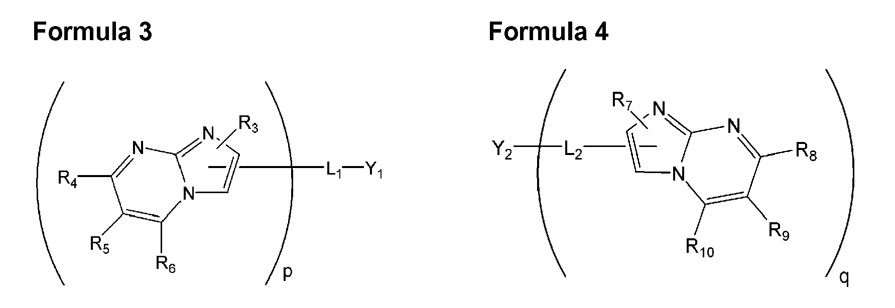
- In Formulae 2 through 4, R1 through R10, L1, L2, Ar1, Ar2, p, q, n, and m are as defined above in connection with Formula 1. The above synthesis method can be performed using a Suzuki reaction.
- The imidazopyrimidine-based compounds of Formula 1 as described above can be used in organic layers of organic light-emitting devices. In detail, according to one embodiment of the present invention, an organic light-emitting device includes a first electrode, a second electrode, and an organic layer between the first and second electrodes. The organic layer includes an imidazopyrimidine-based compound of Formula 1. In one embodiment, the organic layer may be an electron transport layer. The organic light-emitting device may further include at least one of a hole injection layer, a hole transport layer, an electron blocking layer, an emitting layer, a hole blocking layer, an electron transport layer, and an electron injection layer. For example, when the organic layer including the imidazopyrimidine-based compound of Formula 1 is an electron transport layer, the organic light-emitting device according to one embodiment of the present invention may further include a hole injection layer, a hole transport layer, an emitting layer, and an electron injection layer. Moreover, when forming an emitting layer using a phosphorescent material, the organic light-emitting device according to one embodiment of the present invention may further include a hole blocking layer. In addition, various modifications can be made.
- In more detail, an organic light-emitting device according to an embodiment of the present invention is illustrated in
FIG. 1 . Referring toFIG. 1 , an organic light-emitting device has a first electrode/hole injection layer/hole transport layer/emitting layer/electron transport layer/electron injection layer/second electrode structure. In addition, an organic light-emitting device according to another embodiment of the present invention may have a first electrode/hole injection layer/emitting layer/electron transport layer/electron injection layer/second electrode structure, or a first electrode/hole injection layer/hole transport layer/emitting layer/hole blocking layer/electron transport layer/electron injection layer/second electrode structure. Here, the electron transport layer may include a compound of Formula 1. - An emitting layer of an organic light-emitting device according to the present invention may include a phosphorescent or fluorescent dopant generating red, green, blue, or white light. The phosphorescent dopant may be an organometallic compound including at least one element selected from lr, Pt, Os, Ti, Zr, Hf, Eu, Tb, and Tm.
- A method of manufacturing an organic light-emitting device according to an embodiment of the present invention will now be described with reference to
FIG. 1 . First, a first electrode is formed on a substrate by deposition or sputtering using a first electrode material having a high work function. The first electrode may be an anode or a cathode. Here, the substrate may be any substrate commonly used in organic light-emitting devices. The substrate may be a glass or transparent plastic substrate having good mechanical strength, thermal stability, transparency, surface smoothness, handling properties, and water repulsion. The first electrode material may be a material having good conductivity, examples of which include indium tin oxide (ITO), indium zinc oxide (IZO), tin oxide (SnO2), zinc oxide (ZnO), Al, Mg, or Ag. The first electrode may be a transparent electrode, a translucent electrode, or a reflective electrode. Next, a hole injection layer (HIL) may be formed on the first electrode using any one of various methods, e.g., vacuum deposition, spin-coating, casting, or Langmuir-Blodgett (LB) techniques. - When forming the hole injection layer by vacuum deposition, the deposition conditions vary according to the type of hole injection layer material, the structure and thermal characteristics of the hole injection layer, etc. However, in one embodiment, the hole injection layer is deposited at a deposition rate ranging from 0.01 to 100Å/sec, a temperature ranging from 100 to 500° C, and a vacuum pressure ranging from 10-8 to 10-3 torr.
- When forming the hole injection layer by spin-coating, the coating conditions vary according to the type of hole injection layer material, the structure and thermal characteristics of the hole injection layer, etc. However, in one embodiment, the spin-coating is performed at a coating speed ranging from 2,000 to 5,000rpm, and, after the spin-coating, thermal treatment is performed at a temperature ranging from 80 to 200° C to remove solvent.
- The hole injection layer material is not particularly limited and may be any known hole injection layer material. Examples of suitable hole injection layer materials include phthalocyanine compounds (e.g., copper phthalocyanine), Starburst-type amine derivatives (e.g., TCTA, m-MTDATA, m-MTDAPB), soluble conductive polymers, e.g., polyaniline/dodecylbenzenesulfonic acid (Pani/DBSA), poly(3,4-ethylenedioxythiophene)/poly(4-styrenesulfonate) (PEDOT/PSS), polyaniline/camphor sulfonic acid (Pani/CSA), or polyaniline/poly(4-styrenesulfonate) (PANI/PSS).

- The hole injection layer may be formed to a thickness ranging from 100 to 10,000Å. In one embodiment, for example, the hole injection layer is formed to a thickness ranging from 100 to 1,000Å. When the thickness of the hole injection layer is within these ranges, proper hole injection characteristics can be obtained and increases in driving voltage can be substantially prevented. Next, a hole transport layer (HTL) may be formed on the hole injection layer using various methods, e.g., vacuum deposition, spin-coating, casting, or LB techniques. When forming the hole transport layer using vacuum deposition or spin-coating, the deposition or coating conditions vary according to the type of compound used, but are generally the same as those for the formation of the hole injection layer.
- The hole transport layer material is not particularly limited and may be any known hole transport layer material, e.g., carbazole derivatives (such as N-phenylcarbazole or polyvinylcarbazole), amine derivatives having a fused aromatic ring (such as
- N,N'-bis(3-methylphenyl)-N,N'-diphenyl-[1,1-biphenyl]-4,4'-diamine (TPD) or N,N'-di(naphthalene-1-yl)-N,N'-diphenylbenzidine (α-NPD)), and the like.


- The hole transport layer may be formed to a thickness ranging from 50 to 1,000Å. In one embodiment, for example, the hole transport layer may be formed to a thickness ranging from 100 to 600Å. When the thickness of the hole transport layer is within these ranges, proper hole transport characteristics can be obtained and increases in driving voltage can be substantially prevented. Next, an emitting layer (EML) may be formed on the hole transport layer using vacuum deposition, spin-coating, casting, or LB techniques. When forming the emitting layer using vacuum deposition or spin-coating, the deposition or coating conditions vary according to the type of compound used, but are generally the same as those for the formation of the hole injection layer.
- The emitting layer may be formed using any known emitting material. The emitting layer may also be formed using any known host and dopant. With respect to the dopant, known fluorescent dopants and known phosphorescent dopants can be used. Nonlimiting examples of suitable hosts include Alq3, 4,4'-N,N'-dicarbazole-biphenyl (CBP), poly(n-vinylcarbazole) (PVK), distyrylarylene (DSA), and the like.
- Examples of suitable dopants include Ir(ppy)3(ppy = phenylpyridine) (green), (4,6-F2ppy)2Irpic, PtOEP (platinum(II) octaethylporphyrin), compounds represented by Formula 5, Firpic, TBPe, and the like.

- The dopant may be present in an amount ranging from 0.1 to 20 parts by weight based on 100 parts by weight (the total weight of the host and the dopant) of the emitting layer material. In one embodiment, for example, the dopant may be present in an amount ranging from 0.5 to 12 parts by weight based on 100 parts by weight (the total weight of the host and the dopant) of the emitting layer material. When the content of the dopant is within these ranges, phosphorescence and fluorescence concentration quenching can be substantially prevented.
- The emitting layer may be formed to a thickness ranging from 100 to 1,000Å. In one embodiment, for example, the emitting layer may be formed to a thickness ranging from 200 to 600Å. When the thickness of the emitting layer is within these ranges, proper emission characteristics can be obtained and increases in driving voltage can be substantially prevented.
- When the emitting layer includes a phosphorescent dopant, a hole blocking layer (HBL) (not shown in
FIG. 1 ) may be formed on the emitting layer to prevent diffusion of triplet excitons or holes into the electron transport layer. The hole blocking layer material is not particularly limited, and may be any known hole blocking layer material, e.g., oxadiazole derivatives, triazole derivatives, phenanthroline derivatives, Balq, BCP, and the like. - The hole blocking layer may be formed to a thickness ranging from 50 to 1,000Å. In one embodiment, for example, the hole blocking layer may be formed to a thickness ranging from 100 to 300Å. When the thickness of the hole blocking layer is within these range, proper hole blocking characteristics can be obtained and increases in driving voltage can be substantially prevented.
- Next, an electron transport layer (ETL) may be formed using various methods, e.g., vacuum deposition, spin-coating, or casting. When forming the electron transport layer using vacuum deposition or spin-coating, the deposition or coating conditions vary according to the type of compound used, but are generally the same as those for the formation of the hole injection layer.
- The electron transport layer material may be an imidazopyrimidine-based compound of Formula 1 as described above and may be used alone or in combination with a known material. Examples of suitable known electron transport layer materials include quinoline derivatives (such as tris(8-quinolinolate)aluminum (Alq3)), and TAZ.
- The electron transport layer may be formed to a thickness ranging from 100 to 1,000Å. In one embodiment, for example, the electron transport layer may be formed to a thickness ranging from 100 to 500Å. When the thickness of the electron transport layer is within these ranges, proper electron transport characteristics can be obtained and increases in driving voltage can be substantially prevented.
- An electron injection layer (EIL) may be formed on the electron transport layer to facilitate the injection of electrons from a cathode. The electron injection layer material may be any known electron injection layer material, e.g., LiF, NaCl, CsF, Li2O, or BaO. The deposition or coating conditions of the electron injection layer vary according to the type of compound used, but are generally the same as those for the formation of the hole injection layer.
- The electron injection layer may be formed to a thickness ranging from 1 to 100Å. In one embodiment, the electron injection layer may be formed to a thickness ranging from 5 to 90Å. When the thickness of the electron injection layer is within these ranges, proper electron injection characteristics can be obtained and increases in driving voltage can be substantially prevented. Finally, a second electrode may be formed on the electron injection layer by vacuum deposition or sputtering. The second electrode may be a cathode or an anode. The material of the second electrode may be a metal or alloy having a low work function, an electroconductive compound, or a mixture thereof. Examples of suitable materials for the second electrode include lithium (Li), magnesium (Mg), aluminum (Al), aluminum-lithium (Al-Li), calcium (Ca), magnesium-indium (Mg-In), magnesium-silver (Mg-Ag), etc. The second electrode may also be a transmissive cathode formed of ITO or IZO to produce a front-emission type device.
- Synthesis Examples detailing the synthesis of Compounds 1 through 3 and
- Examples detailing the manufacturing of organic light-emitting devices employing organic layers including Compounds 1 through 3 are following.
- Compound 1 was synthesized according to Reaction Scheme 1.

- Copper bromide (10g, 44 mmol) and 2-aminoanthraquinone (8g, 35.8 mmol) were added to 250 ml of bromic acid, and the reaction mixture was heated to 65 ° C. When gas generation was stopped, the reaction solution was cooled to room temperature, added to a 20% HCl solution (1,000 ml), and extracted with dichloromethane. The organic layer was dried over anhydrous magnesium sulfate to remove residual moisture, dried under reduced pressure, and purified by column chromatography (dichloromethane/n-hexane = 4:1) to yield intermediate 1a (7.7g).
- The intermediate 1 a (10g, 34.8mmol) was added to 100 ml of dried THF under a nitrogen atmosphere. The reaction mixture was cooled to -78° C, and 2-naphthyl magnesium bromide (0.5M, 10 mmol) was gradually added thereto. The reaction solution was heated to room temperature and stirred for three hours. An ammonium chloride solution was added thereto and the resultant solution was extracted with methylenechloride. The organic layer was dried over anhydrous magnesium sulfate to remove the solvent, and dissolved in a trace amount of ethylether. Petroleum ether was added thereto and the reaction mixture was stirred for several hours to obtain a solid compound. The solid compound was filtered and dried under vacuum to yield dinaphthyl dialcohol (17.6g).
- The dinaphthyl dialcohol (17.6g, 32.4mmol) was dispersed in 200 ml of acetic acid under a nitrogen atmosphere, and potassium iodide (53.4g, 330mmol) and sodium hypophosphite hydrate (58g, 660mmol) were added thereto. The reaction mixture was stirred and refluxed for three hours. The reaction solution was cooled to room temperature, filtered, washed with water and methanol, and dried under vacuum to yield intermediate 1b as a light yellow powder (11.3g).
- The intermediate 1b (5g, 9.81 mmol) was dissolved in 70 ml of dried THF under a nitrogen atmosphere, and butyl lithium (4.7ml, 11.8mmol) was added dropwise thereto at -78° C. The reaction mixture was stirred at -78° C for one hour, and trimethylborate (2.20ml, 29.4mmol) was added thereto. The reaction solution was heated to room temperature and incubated for one hour. Then, a 2N HCl solution was added thereto, and the resultant solution was stirred for three hours. The resultant solid compound was washed and filtered with toluene to yield intermediate 1c as a light yellow powder (3.27g, yield: 70%).
- 2-aminopyrimidine (3.39g, 35.98mmol) and 2,4'-dibromoacetophenone (10g, 35.98mmol) were dissolved in ethanol (150ml), and the reaction mixture was refluxed for 12 hours. The reaction solution was cooled to room temperature to obtain a white solid. The white solid was washed and filtered with a saturated NaHCO3 solution. The organic layer was dried over anhydrous magnesium sulfate to remove residual moisture, dried under reduced pressure, and recrystallized (in dichloromethane/n-hexane) to yield intermediate 1d as a plate crystal (8.02g, yield: 82%).
- The intermediate 1c (1.85g, 3.90mmol) and the intermediate 1d (1g, 3.90mmol) were added to a mixed solvent of a potassium carbonate solution (2.7g, 19.5mmol) and THF, and Pd(PPh3)4 (225mg, 0.196mmol) was added thereto while stirring. The reaction mixture was refluxed for six hours. The reaction solution was cooled to room temperature, and the resultant solid compound was washed with water, ethanol, and toluene, and filtered to yield Compound 1 as a yellow powder (1.73g, yield: 71 %). (1H NMR (400MHz, CDCl3) 8.51 (1H), 8.40(1H), 8.12(1H), 8.06-7.99(5H), 7.96(2H), 7.85(1H), 7.78-7.59(15H), 7.32(2H), 6.84(1H)).
- Compound 2 (a yellow powder) was synthesized as in Synthesis Example 1 except that phenyl magnesium bromide was used instead of 2-naphthyl magnesium bromide in the synthesis of the intermediate 1b. (1H NMR (400MHz, CDCl3) 8.54(1H), 8.42(1H), 8.07(2H), 7.96(1H), 7.83(1H), 7.80(1H), 7.73-7.48(15H), 7.35(2H), 6.87(1H)).
- Compound 3 (a yellow powder) was synthesized as in Synthesis Example 1 except that phenyl magnesium bromide was used instead of 2-naphthyl magnesium bromide in the synthesis of the intermediate 1b, and 2,4'-dibromopropiophenone was used instead of dibromoacetophenone in the synthesis of the intermediate 1d. (1H NMR (400MHz, CDCl3) 8.54(1H), 8.22(1H), 7.97(1H), 7.93(2H), 7.70(1H), 7.71-7.52(15H), 7.35(2H), 6.92(1H), 2.73(3H)).
- A 15 Ω/cm2 ITO glass substrate (Corning, 1,200Å) was cut into 50 mm x 50 mm x 0.7 mm pieces and subjected to ultrasonic cleaning in isopropyl alcohol and pure water (5 minutes for each) and UV/ozone cleaning (30 minutes) to form anodes. Then, m-MTDATA was vacuum-deposited on the anodes to form hole injection layers with a thickness of 750Å, and α-NPD was vacuum-deposited on the hole injection layers to form hole transport layers with a thickness of 150Å. DSA (97 wt%) used as a host and TBPe (3 wt%) used as a dopant were co-deposited on the hole transport layers to form emitting layers with a thickness of 300Å. Compound 1 obtained in Synthesis Example 1 was vacuum-deposited on the emitting layers to form electron transport layers with a thickness of 200Å.
- LiF was vacuum-deposited on the electron transport layers to form electron injection layers with a thickness of 80Å, and Al was vacuum-deposited on the electron injection layers to form cathodes with a thickness of 3,000Å, thereby completing the manufacture of organic light-emitting devices.
- Organic light-emitting devices were manufactured as in Example 1 except that Compound 2 obtained in Synthesis Example 2 was used as an electron transport layer material.
- Organic light-emitting devices were manufactured as in Example 1 except that Compound 3 obtained in Synthesis Example 3 was used as an electron transport layer material.
- Organic light-emitting devices were manufactured as in Example 1 except that Alq3 (8-hydroxyquinoline aluminum complex) was used as an electron transport layer material.
- The current density (mA/cm2), driving voltage (V), brightness (cd/m2), and efficiency (lm/W) of the organic light-emitting devices manufactured in Examples 1-3 and Comparative Example 1 were evaluated using a PR650 (Spectroscan) Source Measurement Unit (manufactured by PhotoResearch), and the results are presented in Table 1 below.
Table 1 Sample Current density (mA/cm2) Driving voltage (V) Brightness (cd/m2) Efficiency (lm/W) Example 1 10 4.1 860 6.54 Example 2 10 4.0 834 6.46 Example 3 10 4.6 771 5.28 Comparative Example 1 10 5.9 581 2.90 - As shown in Table 1, the organic light-emitting devices manufactured in Examples 1-3 exhibited better current density, driving voltage, brightness, and efficiency characteristics than the organic light-emitting devices manufactured in Comparative Example 1. These results show that an organic light-emitting device employing an organic layer including an imidazopyrimidine compound of Formula 1 according to embodiments of the present invention exhibit higher brightness, higher efficiency, lower driving voltages, and longer lifetimes than conventional organic light-emitting devices.
- The imidazopyrimidine-based compounds of Formula 1 according to embodiments of the present invention have good electron transport capabilities. Thus, organic light-emitting devices employing organic layers including imidazopyrimidine-based compounds can exhibit lower driving voltages, higher brightness, higher efficiency, lower power consumption, and longer lifetimes.
Claims (15)
- An imidazopyrimidine-based compound represented by Formula 1:
 each of R1, R2, R3, R4, R5, R6, R7, R8, R9, and R10 is independently selected from the group consisting of hydrogen, halogens, hydroxy, cyano, substituted and unsubstituted C1-C30 alkyl groups, substituted and unsubstituted C1-C30 alkoxy groups, substituted and unsubstituted C1-C30 acyl groups, substituted and unsubstituted C2-C30 alkenyl groups, substituted and unsubstituted C2-C30 alkynyl groups, substituted and unsubstituted C6-C30 aryl groups, and substituted and unsubstituted C3-C30 heteroaryl groups, wherein at least two adjacent groups selected from the group consisting of R4 through R6 are joined together to form a saturated or unsaturated ring, and wherein at least two adjacent groups selected from the group consisting of R8 through R10 are joined together to form a saturated or unsaturated ring;each of L1 and L2 is independently selected from the group consisting of single bonds, substituted and unsubstituted C1-C30 alkylene groups, substituted and unsubstituted C6-C30 arylene groups, and substituted and unsubstituted C3-C30 heteroarylene groups;each of Ar1 and Ar2 is independently selected from the group consisting of substituted and unsubstituted C6-C30 aryl groups, and substituted and unsubstituted C3-C30 heteroaryl groups;each of p and q is an integer ranging from 1 to 5; andeach of m and n is an integer ranging from 0 to 4, wherein a sum of m and n is not zero.
 - The imidazopyrimidine-based compound of claim 1, wherein each of R1 through R10 is independently selected from the group consisting of hydrogen, substituted and unsubstituted C1-C10 alkyl groups, substituted and unsubstituted C2-C10 alkenyl groups, substituted and unsubstituted C6-C12 aryl groups, and substituted and unsubstituted C3-C12 heteroaryl groups.
- The imidazopyrimidine-based compound of claim 2, wherein each of R1 through R10 is independently selected from the group consisting of hydrogen, C1-C10 alkyl groups, C1-C10 haloalkyl groups, C2-C10 alkenyl groups, C2-C10 haloalkenyl groups, phenyl, halophenyl groups, C1-C10 alkylphenyl groups, C1-C10 alkoxyphenyl groups, naphthyl, halonaphthyl groups, C1-C10 alkylnaphthyl groups, and C1-C10 alkoxynaphthyl groups.
- The imidazopyrimidine-based compound of any of claims 1 through 3, wherein at least two adjacent groups selected from the group consisting of R4 through R6 and/or at least two adjacent groups selected from the group consisting of R8 through R10 are joined together to form a substituted or unsubstituted C6-C12 aromatic ring.
- The imidazopyrimidine-based compound of any of claims 1 through 4, wherein each of L1 and L2 is independently selected from the group consisting of substituted and unsubstituted C6-C12 arylene groups, and substituted and unsubstituted C3-C12 heteroarylene groups.
- The imidazopyrimidine-based compound of claim 5, wherein each of L1 and L2 is independently selected from the group consisting of phenylene, halophenylene groups, C1-C10 alkylphenylene groups, C1-C10 alkoxyphenylene groups, naphthylene, halonaphthylene groups, C1-C10 alkylnaphthylene groups, and C1-C10 alkoxynaphthylene groups.
- The imidazopyrimidine-based compound of any of claims 1 through 6, wherein each of Ar1 and Ar2 is independently selected from the group consisting of substituted and unsubstituted C6-C12 aryl groups, and substituted and unsubstituted C3-C12 heteroaryl groups.
- The imidazopyrimidine-based compound of claim 7, wherein each of Ar1 and Ar2 is independently selected from the group consisting of phenyl, halophenyl groups, C1-C10 alkylphenyl groups, C1-C10 alkoxyphenyl groups, naphthyl, halonaphthyl groups, C1-C10 alkylnaphthyl groups, C1-C10 alkoxynaphthyl groups, pyridinyl, halopyridinyl groups, C1-C10 alkylpyridinyl groups, C1-C10 alkoxypyridinyl groups, quinolinyl, haloquinolinyl groups, C1-C10 alkylquinolinyl groups, C1-C10 alkoxyquinolinyl groups, isoquinolinyl, haloisoquinolinyl groups, C1-C10 alkylisoquinolinyl groups, and C1-C10 alkoxyisoquinolinyl groups.
- The imidazopyrimidine-based compound of any of claims 1 through 8, wherein m is 0 and n is 1.
- The imidazopyrimidine-based compound of any of claims 1 through 9, wherein each of m and n is 1.
- The imidazopyrimidine-based compound of claim 1, wherein the compound represented by Formula 1 is selected from the group consisting of Compounds 1 through 9:


- An organic light-emitting device comprising:a first electrode;a second electrode; andan organic layer between the first electrode and the second electrode, the organic layer comprising the imidazopyrimidine-based compound of any of claims 1 through 11.
- The organic light-emitting device of claim 12, wherein the organic layer is an electron transport layer.
- The organic light-emitting device of claim 13, further comprising a layer between the first and second electrodes, the layer being selected from the group consisting of hole injection layers, hole transport layers, electron blocking layers, emitting layers, hole blocking layers, electron injection layers, and combinations thereof.
- The organic light-emitting device of claim 12, wherein the organic layer is an electron transport layer, and the organic light-emitting device further comprises a hole injection layer, a hole transport layer, an emitting layer, and an electron injection layer between the first electrode and the second electrode.
Applications Claiming Priority (1)
| Application Number | Priority Date | Filing Date | Title |
|---|---|---|---|
| KR1020070024697A KR100852118B1 (en) | 2007-03-13 | 2007-03-13 | An imidazopyrimidine compound and an organic light emitting device comprising an organic film |
Publications (2)
| Publication Number | Publication Date |
|---|---|
| EP1970376A1 true EP1970376A1 (en) | 2008-09-17 |
| EP1970376B1 EP1970376B1 (en) | 2009-11-18 |
Family
ID=39401203
Family Applications (1)
| Application Number | Title | Priority Date | Filing Date |
|---|---|---|---|
| EP08102100A Ceased EP1970376B1 (en) | 2007-03-13 | 2008-02-28 | Imidazopyrimidine-based compound and organic light-emitting device employing organic layer including the same |
Country Status (7)
| Country | Link |
|---|---|
| US (1) | US7824780B2 (en) |
| EP (1) | EP1970376B1 (en) |
| JP (1) | JP4787277B2 (en) |
| KR (1) | KR100852118B1 (en) |
| CN (1) | CN101265260B (en) |
| DE (1) | DE602008000270D1 (en) |
| TW (1) | TWI388561B (en) |
Families Citing this family (8)
| Publication number | Priority date | Publication date | Assignee | Title |
|---|---|---|---|---|
| KR100994115B1 (en) * | 2008-08-18 | 2010-11-15 | 삼성모바일디스플레이주식회사 | Organic light emitting device having a light efficiency improving layer |
| US9150536B2 (en) | 2009-01-20 | 2015-10-06 | Lg Chem, Ltd. | Cycloalkene derivatives and organic electronic devices using the same |
| KR101645949B1 (en) * | 2009-03-23 | 2016-08-05 | 롬엔드하스전자재료코리아유한회사 | Electroluminescent device using the electroluminescent compounds |
| KR101910996B1 (en) | 2011-05-13 | 2018-10-24 | 삼성디스플레이 주식회사 | Condensed-cyclic compound, organic light-emitting diode comprising the same and flat display device |
| KR101857250B1 (en) | 2011-05-13 | 2018-05-14 | 삼성디스플레이 주식회사 | Condensed-cyclic compound, organic light-emitting diode comprising the same and flat display device |
| JP6119521B2 (en) * | 2013-09-19 | 2017-04-26 | コニカミノルタ株式会社 | Transparent electrode, electronic device, and organic electroluminescence element |
| CN104650117B (en) * | 2013-12-26 | 2017-08-01 | 北京鼎材科技有限公司 | A kind of organic compound and its application in organic electroluminescence device |
| CN108644628B (en) | 2018-06-06 | 2024-03-29 | 北京夏禾科技有限公司 | High-yield low-cost large-area flexible OLED (organic light emitting diode) lighting module |
Citations (4)
| Publication number | Priority date | Publication date | Assignee | Title |
|---|---|---|---|---|
| US6620529B1 (en) * | 1999-10-27 | 2003-09-16 | Fuji Photo Film Co., Ltd. | Materials for light emitting devices and light emitting devices using the same |
| EP1582516A1 (en) | 2003-01-10 | 2005-10-05 | Idemitsu Kosan Co., Ltd. | Nitrogenous heterocyclic derivative and organic electroluminescent element employing the same |
| WO2007069847A1 (en) * | 2005-12-13 | 2007-06-21 | Lg Chem. Ltd. | Novel imidazoquinazoline derivative, process for preparing the same, and organic electronic device using the same |
| JP2008069100A (en) * | 2006-09-13 | 2008-03-27 | Tdk Corp | Compound for organic el element and organic el element |
Family Cites Families (12)
| Publication number | Priority date | Publication date | Assignee | Title |
|---|---|---|---|---|
| US4356429A (en) * | 1980-07-17 | 1982-10-26 | Eastman Kodak Company | Organic electroluminescent cell |
| US6559256B2 (en) | 1994-12-28 | 2003-05-06 | Cambridge Display Technology Ltd. | Polymers for use in optical devices |
| JPH11329734A (en) | 1998-03-10 | 1999-11-30 | Mitsubishi Chemical Corp | Organic electroluminescent device |
| JP4032566B2 (en) * | 1999-06-21 | 2008-01-16 | 東レ株式会社 | Light emitting element |
| JP4646494B2 (en) * | 2002-04-11 | 2011-03-09 | 出光興産株式会社 | Novel nitrogen-containing heterocyclic derivative and organic electroluminescence device using the same |
| JPWO2004028217A1 (en) * | 2002-09-20 | 2006-01-19 | 出光興産株式会社 | Organic electroluminescence device |
| JP4693336B2 (en) * | 2003-01-14 | 2011-06-01 | 出光興産株式会社 | Nitrogen-containing heterocyclic derivative and organic electroluminescence device using the same |
| CN101219987A (en) * | 2003-01-10 | 2008-07-16 | 出光兴产株式会社 | Nitrogen-containing heterocyclic derivative and organic electroluminescent element using same |
| WO2005006816A1 (en) * | 2003-07-11 | 2005-01-20 | Idemitsu Kosan Co., Ltd. | White organic electroluminescence device |
| JP4363098B2 (en) * | 2003-07-11 | 2009-11-11 | 三菱化学株式会社 | Bisimidazopyrazinone derivatives and bisaminopyrazine derivatives |
| KR100537621B1 (en) | 2004-02-02 | 2005-12-19 | 삼성에스디아이 주식회사 | Iridium compound and organic electroluminescent display device using the same |
| TWI302907B (en) * | 2004-09-24 | 2008-11-11 | Lg Chemical Ltd | New compound and organic light emitting device using the same (7) |
-
2007
- 2007-03-13 KR KR1020070024697A patent/KR100852118B1/en active Active
-
2008
- 2008-01-09 JP JP2008002392A patent/JP4787277B2/en not_active Expired - Fee Related
- 2008-01-18 TW TW097101973A patent/TWI388561B/en not_active IP Right Cessation
- 2008-02-08 US US12/028,744 patent/US7824780B2/en active Active
- 2008-02-28 DE DE602008000270T patent/DE602008000270D1/en active Active
- 2008-02-28 EP EP08102100A patent/EP1970376B1/en not_active Ceased
- 2008-03-12 CN CN200810086441.2A patent/CN101265260B/en not_active Expired - Fee Related
Patent Citations (4)
| Publication number | Priority date | Publication date | Assignee | Title |
|---|---|---|---|---|
| US6620529B1 (en) * | 1999-10-27 | 2003-09-16 | Fuji Photo Film Co., Ltd. | Materials for light emitting devices and light emitting devices using the same |
| EP1582516A1 (en) | 2003-01-10 | 2005-10-05 | Idemitsu Kosan Co., Ltd. | Nitrogenous heterocyclic derivative and organic electroluminescent element employing the same |
| WO2007069847A1 (en) * | 2005-12-13 | 2007-06-21 | Lg Chem. Ltd. | Novel imidazoquinazoline derivative, process for preparing the same, and organic electronic device using the same |
| JP2008069100A (en) * | 2006-09-13 | 2008-03-27 | Tdk Corp | Compound for organic el element and organic el element |
Non-Patent Citations (1)
| Title |
|---|
| DATABASE CAPLUS [online] CHEMICAL ABSTRACTS SERVICE, COLUMBUS, OHIO, US; 2008, EBISAWA, AKIRA ET AL: "Anthracenes and organic electroluminescent devices using them as electron-injecting and -transporting agents", XP002481489, retrieved from STN Database accession no. 2008:373117 * |
Also Published As
| Publication number | Publication date |
|---|---|
| TWI388561B (en) | 2013-03-11 |
| CN101265260B (en) | 2014-01-29 |
| CN101265260A (en) | 2008-09-17 |
| JP2008222706A (en) | 2008-09-25 |
| KR100852118B1 (en) | 2008-08-13 |
| EP1970376B1 (en) | 2009-11-18 |
| JP4787277B2 (en) | 2011-10-05 |
| US20080226945A1 (en) | 2008-09-18 |
| DE602008000270D1 (en) | 2009-12-31 |
| US7824780B2 (en) | 2010-11-02 |
| TW200902534A (en) | 2009-01-16 |
Similar Documents
| Publication | Publication Date | Title |
|---|---|---|
| EP1925618B1 (en) | Imidazopyridine-based compounds and organic light emitting diode including organic layer comprising the imidazopyridine-based compounds | |
| EP1862524B1 (en) | Organic light emitting device and flat panel display device comprising the same | |
| KR100903102B1 (en) | An imidazopyridine-based compound and an organic light emitting diode employing an organic layer comprising the same | |
| EP1921082B1 (en) | Silanylamine-based compound, method of preparing the same and organic light emitting device including organic layer comprising the silanylamine-based compound | |
| KR100994115B1 (en) | Organic light emitting device having a light efficiency improving layer | |
| KR101528241B1 (en) | An aromatic cyclic compound, an organic light emitting device having an organic film containing the same, and a method for manufacturing the organic light emitting device | |
| EP2110373B1 (en) | Bipyridine-based compound and organic light emitting diode employing organic layer comprising the same | |
| EP2292601B1 (en) | Phenanthro[2,3-b]pyrroles and Phenanthro[3,2-b]pyrroles for organic light-emitting devices | |
| EP1970376B1 (en) | Imidazopyrimidine-based compound and organic light-emitting device employing organic layer including the same | |
| KR20150007605A (en) | Iridium complex and Organic light emitting device comprising the same | |
| EP2392563A1 (en) | Nitrogen containing polycyclic derivatives useful in organic light-emitting devices | |
| EP2298771B1 (en) | Organic Light-Emitting Device | |
| US7754349B2 (en) | Silanylamine-based compound and organic light-emitting device including organic layer including the silanylamine-based compound | |
| US20090230855A1 (en) | Novel organic compound and organic light emitting device comprising the same | |
| EP2301920A1 (en) | Organic light emitting device containing naphthoindole derivatives | |
| KR20090018503A (en) | Oxadiazole derivative compound and organic light emitting device having the same | |
| KR100898073B1 (en) | Quinoxaline ring-containing compound and organic light emitting device using the same | |
| KR100730178B1 (en) | Carbazole ring-containing silicon-based compound and organic light-emitting device having an organic film comprising the same |
Legal Events
| Date | Code | Title | Description |
|---|---|---|---|
| PUAI | Public reference made under article 153(3) epc to a published international application that has entered the european phase |
Free format text: ORIGINAL CODE: 0009012 |
|
| 17P | Request for examination filed |
Effective date: 20080228 |
|
| AK | Designated contracting states |
Kind code of ref document: A1 Designated state(s): AT BE BG CH CY CZ DE DK EE ES FI FR GB GR HR HU IE IS IT LI LT LU LV MC MT NL NO PL PT RO SE SI SK TR |
|
| AX | Request for extension of the european patent |
Extension state: AL BA MK RS |
|
| RAP1 | Party data changed (applicant data changed or rights of an application transferred) |
Owner name: SAMSUNG MOBILE DISPLAY CO., LTD. |
|
| AKX | Designation fees paid |
Designated state(s): DE FR GB HU IT PL |
|
| GRAP | Despatch of communication of intention to grant a patent |
Free format text: ORIGINAL CODE: EPIDOSNIGR1 |
|
| GRAS | Grant fee paid |
Free format text: ORIGINAL CODE: EPIDOSNIGR3 |
|
| GRAA | (expected) grant |
Free format text: ORIGINAL CODE: 0009210 |
|
| RIN1 | Information on inventor provided before grant (corrected) |
Inventor name: KIM, HEE-YEON Inventor name: LEE, CHANG-HO Inventor name: SHIN, JUNG-HAN Inventor name: YANG, SEUNG-GAK Inventor name: KO, HEE-JOO |
|
| AK | Designated contracting states |
Kind code of ref document: B1 Designated state(s): DE FR GB HU IT PL |
|
| REG | Reference to a national code |
Ref country code: GB Ref legal event code: FG4D |
|
| REF | Corresponds to: |
Ref document number: 602008000270 Country of ref document: DE Date of ref document: 20091231 Kind code of ref document: P |
|
| REG | Reference to a national code |
Ref country code: DE Ref legal event code: R096 Ref document number: 602008000270 Country of ref document: DE Effective date: 20091231 |
|
| PG25 | Lapsed in a contracting state [announced via postgrant information from national office to epo] |
Ref country code: PL Free format text: LAPSE BECAUSE OF FAILURE TO SUBMIT A TRANSLATION OF THE DESCRIPTION OR TO PAY THE FEE WITHIN THE PRESCRIBED TIME-LIMIT Effective date: 20091118 |
|
| PLBE | No opposition filed within time limit |
Free format text: ORIGINAL CODE: 0009261 |
|
| STAA | Information on the status of an ep patent application or granted ep patent |
Free format text: STATUS: NO OPPOSITION FILED WITHIN TIME LIMIT |
|
| 26N | No opposition filed |
Effective date: 20100819 |
|
| REG | Reference to a national code |
Ref country code: DE Ref legal event code: R097 Ref document number: 602008000270 Country of ref document: DE Effective date: 20100819 |
|
| PG25 | Lapsed in a contracting state [announced via postgrant information from national office to epo] |
Ref country code: IT Free format text: LAPSE BECAUSE OF FAILURE TO SUBMIT A TRANSLATION OF THE DESCRIPTION OR TO PAY THE FEE WITHIN THE PRESCRIBED TIME-LIMIT Effective date: 20091118 |
|
| REG | Reference to a national code |
Ref country code: DE Ref legal event code: R082 Ref document number: 602008000270 Country of ref document: DE Representative=s name: GULDE HENGELHAUPT ZIEBIG & SCHNEIDER, DE |
|
| PG25 | Lapsed in a contracting state [announced via postgrant information from national office to epo] |
Ref country code: HU Free format text: LAPSE BECAUSE OF FAILURE TO SUBMIT A TRANSLATION OF THE DESCRIPTION OR TO PAY THE FEE WITHIN THE PRESCRIBED TIME-LIMIT Effective date: 20100519 |
|
| REG | Reference to a national code |
Ref country code: DE Ref legal event code: R081 Ref document number: 602008000270 Country of ref document: DE Owner name: SAMSUNG DISPLAY CO., LTD., KR Free format text: FORMER OWNER: SAMSUNG MOBILE DISPLAY CO. LTD., SUWON, KR Effective date: 20120921 Ref country code: DE Ref legal event code: R082 Ref document number: 602008000270 Country of ref document: DE Representative=s name: GULDE HENGELHAUPT ZIEBIG & SCHNEIDER, DE Effective date: 20120921 Ref country code: DE Ref legal event code: R082 Ref document number: 602008000270 Country of ref document: DE Representative=s name: GULDE & PARTNER PATENT- UND RECHTSANWALTSKANZL, DE Effective date: 20120921 Ref country code: DE Ref legal event code: R081 Ref document number: 602008000270 Country of ref document: DE Owner name: SAMSUNG DISPLAY CO., LTD., YONGIN-CITY, KR Free format text: FORMER OWNER: SAMSUNG MOBILE DISPLAY CO. LTD., SUWON, GYEONGGI, KR Effective date: 20120921 |
|
| REG | Reference to a national code |
Ref country code: GB Ref legal event code: 732E Free format text: REGISTERED BETWEEN 20130110 AND 20130116 |
|
| REG | Reference to a national code |
Ref country code: FR Ref legal event code: TP Owner name: SAMSUNG MOBILE DISPLAY CO., LTD., KR Effective date: 20130220 |
|
| REG | Reference to a national code |
Ref country code: FR Ref legal event code: PLFP Year of fee payment: 9 |
|
| REG | Reference to a national code |
Ref country code: FR Ref legal event code: PLFP Year of fee payment: 10 |
|
| REG | Reference to a national code |
Ref country code: FR Ref legal event code: PLFP Year of fee payment: 11 |
|
| P01 | Opt-out of the competence of the unified patent court (upc) registered |
Effective date: 20230515 |
|
| PGFP | Annual fee paid to national office [announced via postgrant information from national office to epo] |
Ref country code: DE Payment date: 20240122 Year of fee payment: 17 Ref country code: GB Payment date: 20240122 Year of fee payment: 17 |
|
| PGFP | Annual fee paid to national office [announced via postgrant information from national office to epo] |
Ref country code: FR Payment date: 20240123 Year of fee payment: 17 |
|
| REG | Reference to a national code |
Ref country code: DE Ref legal event code: R119 Ref document number: 602008000270 Country of ref document: DE |
|
| GBPC | Gb: european patent ceased through non-payment of renewal fee |
Effective date: 20250228 |
|
| PG25 | Lapsed in a contracting state [announced via postgrant information from national office to epo] |
Ref country code: DE Free format text: LAPSE BECAUSE OF NON-PAYMENT OF DUE FEES Effective date: 20250902 |
|
| PG25 | Lapsed in a contracting state [announced via postgrant information from national office to epo] |
Ref country code: GB Free format text: LAPSE BECAUSE OF NON-PAYMENT OF DUE FEES Effective date: 20250228 |
|
| PG25 | Lapsed in a contracting state [announced via postgrant information from national office to epo] |
Ref country code: FR Free format text: LAPSE BECAUSE OF NON-PAYMENT OF DUE FEES Effective date: 20250228 |