EP1968364A1 - Wired circuit board and producing method thereof - Google Patents
Wired circuit board and producing method thereof Download PDFInfo
- Publication number
- EP1968364A1 EP1968364A1 EP08150950A EP08150950A EP1968364A1 EP 1968364 A1 EP1968364 A1 EP 1968364A1 EP 08150950 A EP08150950 A EP 08150950A EP 08150950 A EP08150950 A EP 08150950A EP 1968364 A1 EP1968364 A1 EP 1968364A1
- Authority
- EP
- European Patent Office
- Prior art keywords
- thin film
- circuit board
- wired circuit
- portions
- metal thin
- Prior art date
- Legal status (The legal status is an assumption and is not a legal conclusion. Google has not performed a legal analysis and makes no representation as to the accuracy of the status listed.)
- Granted
Links
Images



Classifications
-
- H—ELECTRICITY
- H05—ELECTRIC TECHNIQUES NOT OTHERWISE PROVIDED FOR
- H05K—PRINTED CIRCUITS; CASINGS OR CONSTRUCTIONAL DETAILS OF ELECTRIC APPARATUS; MANUFACTURE OF ASSEMBLAGES OF ELECTRICAL COMPONENTS
- H05K3/00—Apparatus or processes for manufacturing printed circuits
- H05K3/22—Secondary treatment of printed circuits
- H05K3/24—Reinforcing of the conductive pattern
- H05K3/243—Reinforcing of the conductive pattern characterised by selective plating, e.g. for finish plating of pads
-
- H—ELECTRICITY
- H05—ELECTRIC TECHNIQUES NOT OTHERWISE PROVIDED FOR
- H05K—PRINTED CIRCUITS; CASINGS OR CONSTRUCTIONAL DETAILS OF ELECTRIC APPARATUS; MANUFACTURE OF ASSEMBLAGES OF ELECTRICAL COMPONENTS
- H05K3/00—Apparatus or processes for manufacturing printed circuits
- H05K3/38—Improvement of the adhesion between the insulating substrate and the metal
- H05K3/382—Improvement of the adhesion between the insulating substrate and the metal by special treatment of the metal
- H05K3/384—Improvement of the adhesion between the insulating substrate and the metal by special treatment of the metal by plating
-
- H—ELECTRICITY
- H05—ELECTRIC TECHNIQUES NOT OTHERWISE PROVIDED FOR
- H05K—PRINTED CIRCUITS; CASINGS OR CONSTRUCTIONAL DETAILS OF ELECTRIC APPARATUS; MANUFACTURE OF ASSEMBLAGES OF ELECTRICAL COMPONENTS
- H05K1/00—Printed circuits
- H05K1/02—Details
- H05K1/03—Use of materials for the substrate
- H05K1/05—Insulated conductive substrates, e.g. insulated metal substrate
- H05K1/056—Insulated conductive substrates, e.g. insulated metal substrate the metal substrate being covered by an organic insulating layer
-
- H—ELECTRICITY
- H05—ELECTRIC TECHNIQUES NOT OTHERWISE PROVIDED FOR
- H05K—PRINTED CIRCUITS; CASINGS OR CONSTRUCTIONAL DETAILS OF ELECTRIC APPARATUS; MANUFACTURE OF ASSEMBLAGES OF ELECTRICAL COMPONENTS
- H05K2201/00—Indexing scheme relating to printed circuits covered by H05K1/00
- H05K2201/09—Shape and layout
- H05K2201/09209—Shape and layout details of conductors
- H05K2201/09372—Pads and lands
- H05K2201/09472—Recessed pad for surface mounting; Recessed electrode of component
-
- H—ELECTRICITY
- H05—ELECTRIC TECHNIQUES NOT OTHERWISE PROVIDED FOR
- H05K—PRINTED CIRCUITS; CASINGS OR CONSTRUCTIONAL DETAILS OF ELECTRIC APPARATUS; MANUFACTURE OF ASSEMBLAGES OF ELECTRICAL COMPONENTS
- H05K2203/00—Indexing scheme relating to apparatus or processes for manufacturing printed circuits covered by H05K3/00
- H05K2203/03—Metal processing
- H05K2203/0361—Stripping a part of an upper metal layer to expose a lower metal layer, e.g. by etching or using a laser
-
- H—ELECTRICITY
- H05—ELECTRIC TECHNIQUES NOT OTHERWISE PROVIDED FOR
- H05K—PRINTED CIRCUITS; CASINGS OR CONSTRUCTIONAL DETAILS OF ELECTRIC APPARATUS; MANUFACTURE OF ASSEMBLAGES OF ELECTRICAL COMPONENTS
- H05K2203/00—Indexing scheme relating to apparatus or processes for manufacturing printed circuits covered by H05K3/00
- H05K2203/05—Patterning and lithography; Masks; Details of resist
- H05K2203/0562—Details of resist
- H05K2203/0577—Double layer of resist having the same pattern
-
- H—ELECTRICITY
- H05—ELECTRIC TECHNIQUES NOT OTHERWISE PROVIDED FOR
- H05K—PRINTED CIRCUITS; CASINGS OR CONSTRUCTIONAL DETAILS OF ELECTRIC APPARATUS; MANUFACTURE OF ASSEMBLAGES OF ELECTRICAL COMPONENTS
- H05K3/00—Apparatus or processes for manufacturing printed circuits
- H05K3/22—Secondary treatment of printed circuits
- H05K3/24—Reinforcing of the conductive pattern
- H05K3/244—Finish plating of conductors, especially of copper conductors, e.g. for pads or lands
-
- H—ELECTRICITY
- H05—ELECTRIC TECHNIQUES NOT OTHERWISE PROVIDED FOR
- H05K—PRINTED CIRCUITS; CASINGS OR CONSTRUCTIONAL DETAILS OF ELECTRIC APPARATUS; MANUFACTURE OF ASSEMBLAGES OF ELECTRICAL COMPONENTS
- H05K3/00—Apparatus or processes for manufacturing printed circuits
- H05K3/22—Secondary treatment of printed circuits
- H05K3/28—Applying non-metallic protective coatings
Definitions
- the present invention relates to a wired circuit board and a producing method thereof and, more particularly, to a wired circuit board such as a flexible wired circuit board or a suspension board with circuit and a producing method thereof.
- a wired circuit board such as a flexible wired circuit board or a suspension board with circuit includes, e.g., an insulating base layer made of a polyimide resin or the like, a conductive layer formed on the insulating base layer, made of copper or the like, and including wires and terminal portions, and an insulating cover layer formed on the insulating base layer and made of a polyimide resin or the like to cover the conductive layer.
- a wired circuit board is widely used in the field of various electric and electronic equipment.
- a suspension board with circuit 31 as shown in FIG. 5 (a) is proposed as such a wired circuit board, in which, e.g., a nickel thin film 35 is formed on the surface of a copper conductive layer 34 formed on an insulating layer 33 supported by a stainless steel foil base material 32 to cover and protect the surface of the copper conductive layer 34 (see, e.g., Japanese Unexamined Patent No. 10-129831 ).
- the nickel thin film 35 formed on the surface of a terminal portion 38 exposed from an opening portion 41 in an insulating cover layer 36 is removed by etching using the insulating cover layer 36 as an etching resist, and then a terminal is formed on the surface of the terminal portion 38 by electrolytic plating.
- An object of the present invention is to provide a wired circuit board which prevents corrosion and discoloration of a conductive pattern while preventing migration in a conductive pattern, and a producing method thereof.
- a wired circuit board of the present invention comprises an insulating base layer, a conductive pattern formed on the insulating base layer and including a wire and a terminal portion, an insulating cover layer formed on the insulating base layer and having an opening portion to expose the terminal portion, and a metal thin film including a protecting portion interposed between the wire and the insulating cover layer, and an exposed portion formed continuously from the protecting portion on a peripheral end portion of the terminal portion exposed from the opening portion.
- the metal thin film is made of nickel.
- the wired circuit board of the present invention further comprises a plating layer formed in the opening portion.
- the exposed portion formed continuously from the protecting portion is formed on the peripheral end portion of the terminal portion exposed from the opening portion.
- the protecting portion and the exposed portion are continuously formed between the insulating cover layer and the conductive pattern around the opening portion.
- a producing method of a wired circuit board of the present invention comprises the steps of preparing an insulating base layer, forming a conductive pattern including a wire and a terminal portion on the insulating base layer, covering the conductive pattern with a metal thin film, forming an insulating cover layer having an opening portion to expose the terminal portion on the metal thin film, forming an etching resist on the metal thin film on a peripheral end portion of the terminal portion exposed from the opening portion, removing the metal thin film exposed from the etching resist in the terminal portion by etching, and removing the etching resist.
- the metal thin film is made of nickel.
- the producing method of the wired circuit board of the present invention further comprises a step of forming a plating layer in the opening portion.
- the metal thin film on the terminal portion exposed from the opening portion is removed by etching, while protecting the metal thin film on the peripheral end portion of the terminal portion exposed from the opening portion with the etching resist.
- the exposed portion formed continuously from the protecting portion can be formed easily and reliably on the peripheral end portion of the terminal portion exposed from the opening portion. This prevents of corrosion and discoloration of the terminal portion by means of the metal thin film while preventing migration in the conductive pattern.
- FIG. 1 is a schematic plan view showing an embodiment of a wired circuit board according to the present invention.
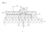
- FIG. 2 is a partial cross-sectional view in the longitudinal direction of the wired circuit board shown in FIG. 1 .
- an insulating base layer 3, a nickel plating layer 12, and a gold plating layer 13, each described later, are omitted for clear illustration of a relative position of a conductive pattern 4 and a cover opening portion 11.
- the wired circuit board 1 is a wired circuit board such as a flexible wired circuit board or a suspension board with circuit. As shown in FIG. 2 , the wired circuit board 1 includes a metal supporting board 2, the insulating base layer 3 formed on the metal supporting board 2, the conductive pattern 4 formed on the insulating base layer 3, and an insulating cover layer 6 formed on the insulating base layer 3.
- the metal supporting board 2 is provided as a reinforcing layer when the wired circuit board 1 is, e.g., a flexible wired circuit board.
- the metal supporting board 2 is provided as a supporting board (suspension board) for supporting a magnetic head (not shown) mounted thereon.
- the metal supporting board 2 is formed of a thin plate in the shape of a flat plate.
- the metal supporting board 2 is formed as the reinforcing layer, it is provided locally at portions where the reinforcing layer is needed.
- the metal supporting board 2 is formed as the supporting board, it is formed to correspond to the outer shape of the wired circuit board 1.
- the length (longitudinal length) and width (widthwise length) of the metal supporting board 2 are selected appropriately depending on the purpose and application.
- the insulating base layer 3 is formed on the metal supporting board 2 to have a pattern corresponding to a portion where the conductive pattern 4 is formed.
- the length and width of the insulating base layer 3 is selected appropriately to have the shape described above depending on the purpose and application.
- the conductive pattern 4 is formed as a wired circuit pattern integrally and continuously including wires 7 and terminal portions 8 connected to the wires 7.
- the plurality of wires 7 are provided along the longitudinal direction of the wired circuit board 1 and arranged in mutually spaced-apart and parallel relation in a widthwise direction (perpendicular to the longitudinal direction and hereinafter referred to as such).
- the terminal portions 8 are disposed at the both longitudinal ends of the wired circuit board 1 and provided in parallel as wide quadrilateral lands each having a generally rectangular shape when viewed in plan view such that the both ends of the individual wires 7 are connected thereto.
- each of the wires 7 is in the range of, e.g., 10 to 100 ⁇ m, or preferably 15 to 50 ⁇ m.
- the spacing between the individual wires 7 is in the range of, e.g., 10 to 100 ⁇ m, or preferably 15 to 50 ⁇ m.
- the width of each of the terminal portions 8 is in the range of, e.g., 50 to 1000 ⁇ m, or preferably 80 to 500 ⁇ m.
- the length of each of the terminal portions 8 is in the range of, e.g., 10 to 1000 ⁇ m, or preferably 100 to 500 ⁇ m.
- the spacing (length of the interval between the individual terminal portions 8 adjacently arranged in the widthwise direction) between the individual terminal portions 8 is in the range of, e.g., 50 to 1000 ⁇ m, or preferably 80 to 500 ⁇ m.
- the insulating cover layer 6 is formed over the insulating base layer 3 and the conductive pattern 4.
- the insulating cover layer 6 is formed with cover opening portions 11 extending therethrough in the thickness direction to correspond to the respective terminals 8.
- each of the cover opening portions 11 is formed to have a shape similar to and slightly smaller than the terminal portions 8 when viewed in plan view.
- the peripheral end portions of the terminal portions 8 are covered with the insulating cover layer 6 and the inner portions of the peripheral end portions of the terminal portion 8 are exposed from the cover opening portions 11.
- the length and width of the insulating cover layer 6 is selected appropriately to have the shape described above depending on the purpose and application.
- a nickel plating layer 12 and a gold plating layer 13, each as a plating layer, are successively formed on the terminal portions 8 in the cover opening portions 11.
- the wired circuit board 1 includes a metal thin film 5 for covering and protecting the wires 7.
- the metal thin film 5 integrally includes protecting portions 9 and exposed portions 10.
- the protecting portions 9 are formed on the surface of the conductive pattern 4 covered with the insulating cover layer 6. That is, the protecting portions 9 are interposed between the wires 7 and the insulating cover layer 6. More specifically, the protecting portions 9 are formed on the upper surfaces, both widthwise side surfaces, and both longitudinal side surfaces of the wires 7.
- the exposed portions 10 are formed on the peripheral end portions (inner portions of the peripheral end portions of the terminal portions 8 mentioned above) 16 of the terminal portions 8 exposed from the cover opening portions 11, as shown in FIGS. 1 and 2 .
- the exposed portions 10 are formed continuously from the protecting portions 9 so as to protrude from the protecting portions 9 into the cover opening portions 11 of the insulating cover layer 6.
- the exposed portions 10 are interposed between the peripheral end portions 16 of the terminal portions 8 exposed from the cover opening portions 11 and the peripheral end portions of the nickel plating layer 12.
- the width W1 in the longitudinal direction of the exposed portion 10, i.e., the length W1 between the longitudinal end edge of the cover opening portion 11 and the longitudinal end edge of the exposed portion 10 and the width (see FIG. 1 ) W2 in the widthwise direction of the exposed portion 10, i.e., the length W2 between the widthwise end edge of the cover opening portion 11 and the widthwise end edge of the exposed portion 10 may be either the same or different from each other.
- the width N1 and the width W2 is not less than 1 ⁇ m, or preferably not less than 5 ⁇ m, and, e.g., not more than 50 ⁇ m, or preferably not more than 35 ⁇ m.
- width W1 in the longitudinal direction of the exposed portion 10 or the width W2 in the widthwise direction thereof is over the range shown above, mounting may be affected thereby.
- the width W1 or the width W2 is under the range shown above, there may be a case where the protecting portions 10 are removed by over-etching in the etching of the metal thin film 5.
- FIGS. 3 and 4 are partial cross-sectional views in the longitudinal direction showing the process steps of producing the wired circuit board shown in FIG. 2 .
- the metal supporting board 2 is prepared in the method.
- a metal foil made of, e.g., stainless steel, 42-alloy, aluminum, copper-beryllium alloy, or phosphor bronze is used.
- a stainless steel foil is used.
- the thickness of the metal supporting board 2 is in the range of, e.g., 10 to 50 ⁇ m, or preferably 15 to 30 ⁇ m.
- the insulating base layer 3 is formed on the metal supporting board 2.
- the insulating base layer 3 is formed in the foregoing pattern corresponding to the portion where the conductive pattern 4 is formed.
- the insulating base layer 3 is made of a resin such as, e.g., a polyimide resin, a polyamide imide resin, an acrylic resin, a polyether nitrile resin, a polyether sulfone resin, a polyethylene terephthalate resin, a polyethylene naphthalate resin, or a polyvinyl chloride resin.
- a resin such as, e.g., a polyimide resin, a polyamide imide resin, an acrylic resin, a polyether nitrile resin, a polyether sulfone resin, a polyethylene terephthalate resin, a polyethylene naphthalate resin, or a polyvinyl chloride resin.
- the insulating base layer 3 is preferably made of a polyimide resin.
- the method for forming the insulating base layer 3 in the foregoing pattern is not particularly limited and a known method is used.
- a varnish of a photosensitive resin photosensitive polyamic acid resin
- the coated varnish is dried to form a base coating.
- the base coating is exposed to light via a photomask, heated as necessary, and then developed to form a pattern.
- the pattern is cured (imidized) by, e.g., heating at a temperature of not less than 250 °C under a reduced pressure.
- the thickness of the insulating base layer 3 thus formed is in the range of, e.g., 1 to 35 ⁇ m, or preferably 8 to 15 ⁇ m.
- the conductive pattern 4 is formed on the insulating base layer 3.
- the conductive pattern 4 is formed as a wired circuit pattern integrally including the plurality of wires 7 and the terminal portions 8 each described above.
- the conductive pattern 4 is made of a conductive material such as, e.g., copper, nickel, gold, a solder, or an alloy thereof, or preferably made of copper.
- the conductive pattern 4 is formed on the upper surface of the insulating base layer 3 by a known patterning method such as, e.g., a subtractive method or an additive method.
- the conductive pattern 4 is formed by the additive method as the foregoing wired circuit pattern.
- a conductive layer is laminated first on the upper surface of the insulating base layer 3 via an adhesive layer as necessary. Then, an etching resist having the same pattern as the wired circuit pattern is formed on the conductive layer and the conductive layer is etched using the etching resist as a resist. Thereafter, the etching resist is removed.
- a conductive thin film is formed first on the entire surface of the insulating base layer 3.
- the conductive thin film is laminated with laminating a chromium thin film and a copper thin film by sputtering, or preferably by chromium sputtering and copper sputtering.
- a plating resist is formed in a pattern reverse to the wired circuit pattern on the upper surface of the conductive thin film. Then, the conductive pattern 4 is formed on the upper surface of the conductive thin film exposed from the plating resist as the wired circuit pattern by electrolytic plating. Thereafter, the plating resist and the portion of the conductive thin film where the plating resist is laminated are removed.
- the conductive pattern 4 thus formed has a thickness in the range of, e.g., 3 to 20 ⁇ m, or preferably 5 to 20 ⁇ m.
- the conductive pattern 4 is covered with the metal thin film 5.
- a material for forming the metal thin film 5 can include a metal such as, e.g., nickel, gold, tin, chromium, titanium, zirconium, or an alloy thereof.
- nickel can be listed.
- a method for forming the metal thin film 5 can include plating such as, e.g., electrolytic plating or electroless plating, a method for sputtering, e.g., the metal listed above as a target, or the like.
- the metal thin film 5 is formed by electroless plating.
- the metal thin film 5 is formed on the surface of the conductive pattern 4.
- the thickness of the metal thin film 5 thus formed is in the range of, e.g., 0.01 to 0. 5 ⁇ m, or preferably 0.05 to 0.3 ⁇ m.
- the insulating cover layer 6 is formed on the insulating base layer 3 and on the metal thin film 5 formed on the surface of the conductive pattern 4 in a pattern formed with the cover opening portions 11 exposing the terminal portions 8.
- the same insulating material as used to form the insulating base layer 3 is used.
- a photosensitive synthetic resin is used, or more preferably photosensitive polyimide is used.
- a varnish of a photosensitive resin is uniformly coated first on the surfaces of the metal thin film 5 and the insulating base layer 3 by the same method as described above. Subsequently, the coated varnish is dried in the same manner as described above to form a cover coating.
- the cover coating' is exposed to light via a photomask and heated as necessary at a predetermined temperature. Subsequently, by the same method as described above, the portions in which the cover opening portions 11 are formed are removed by development. Thereafter, the cover coating is cured (imidized) by, e.g., heating at a temperature of not less than 250 °C under a reduced pressure to form the insulating cover layer 6.
- the thickness of the insulating cover layer 6 thus formed is in the range of, e.g., 1 to 40 ⁇ m, or preferably 3 to 5 ⁇ m.
- an etching resist 14 is formed on the insulating cover layer 6 and on the metal thin film 5 on the peripheral end portions 16 of the terminal portions 8 exposed from the cover opening portions 11.
- the etching resist 14 is formed to be continuously laminated over the surface of the insulating cover layer 6, the inner peripheral surface of the cover opening portions 11, and the upper surface of the metal thin film 5 on the peripheral end portions 16 of the terminal portions 8 exposed from the cover opening portion 11.
- the etching resist 14 is formed to have the same thickness on the inner peripheral surface of the cover opening portions 11 and on the upper surface of the metal thin film 5 on the peripheral end portions 16 of the terminal portions 8.
- the etching resist 14 is formed in the foregoing pattern by a known photoprocess which performs exposure to light and development using a dry film photoresist or the like.
- the metal thin film 5 exposed from the etching resist 14 is removed by etching.
- the metal thin film 5 is wet-etched using an alkaline solution such as a ferric chloride aqueous solution as an etchant by a dipping method or a spraying method.
- an alkaline solution such as a ferric chloride aqueous solution as an etchant
- the metal thin film 5 exposed from the etching resist 14 formed on the inner peripheral surfaces of the cover opening portions 11 is removed.
- the metal thin film 5 on the peripheral end portions 16 of the terminal portions 8, i.e., the exposed portion 10 is formed.
- the metal thin film 5 is formed in the pattern integrally and continuously including the protecting portions 9 and the exposed portions 10.
- the etching resist 14 is removed.
- the etching resist 14 is removed by a known etching method or stripping.
- the nickel plating layer 12 and the gold plating layer 13 are successively formed in the cover opening portions 11.
- the nickel plating layer 12 and the gold plating layer 13 electroless plating and electrolytic plating are used.
- the nickel plating layer 12 and the gold plating layer 13 are successively formed by electrolytic nickel plating and electrolytic gold plating.
- the thickness of the nickel plating layer 12 thus formed is in the range of, e.g., 0.03 to 0.5 ⁇ m and the thickness of the gold plating layer 13 is in the range of, e.g., 0.5 to 2.5 ⁇ m.
- the metal supporting board 2 is trimmed into a desired shape by chemical etching, whereby the wired circuit board 1 is obtained.
- the exposed portions 10 formed continuously from the protecting portions 9 are formed on the peripheral end portions 16 of the terminal portions 8 exposed from the cover opening portions 11.
- the protecting portions 9 and the exposed portions 10 are formed continuously between the insulating cover layer 6 and the conductive pattern 4 around the cover opening portions 11.
- the nickel plating layer 12 is plated in the cover opening portions 11, it is possible to prevent a plating solution or the like from entering the space between the insulating cover layer 6 and the conductive pattern 4 around the cover opening portions 11. This prevents corrosion and discoloration of the terminal portions 8 while preventing migration in the conductive pattern 4 by means of the metal thin film 5.
- the metal thin film 5 on the terminal portions 8 (except for the peripheral end portions 16) exposed from the cover opening portions 11 is removed by etching, while the metal thin film 5 on the peripheral end portions 16 of the terminal portions 8 exposed from the cover opening portions 11 is protected with the etching resist 14 ( FIGS. 4 (f) and (g) ).
- the exposed portions 10 formed continuously from the protecting portions 9 can be formed easily and reliably on the peripheral end portions 16 of the terminal portions 8 exposed from the cover opening portions 11. This prevents corrosion and discoloration of the terminal portions 8 while preventing migration in the conductive pattern 4 by means of the metal thin film 5.
- the terminal portion 8 is formed of the quadrilateral land.
- the shape thereof is not particularly limited.
- the terminal portion 8 can be formed in an appropriate shape, such as a round land.
- wired circuit board of the present invention has been described above as the wired circuit board 1 including the metal supporting board 2, it is not limited thereto.
- the wired circuit board of the present invention is widely applicable to other wired circuit board such as, e.g., a flexible wired circuit board which does not include the metal supporting board 2.
- a metal supporting board made of a stainless steel foil having a thickness of 20 ⁇ m was prepared (see FIG. 3 (a) ).
- a varnish of a photosensitive polyamic acid resin was uniformly coated on the surface of the metal supporting board using a spin coater. Then, the coated varnish was heated at 90 °C for 15 minutes to form a base coating. Thereafter, the base coating was exposed to light at 700 mJ/cm 2 via a photomask, heated at 190 °C for 10 minutes, and then developed using an alkaline developer. Subsequently, the base coating was cured at 385 °C under a reduced pressure of 1.33 Pa to form an insulating base layer made of polyimide in a pattern corresponding to a portion where a conductive pattern was formed on the metal supporting board (see FIG. 3(b) ). The thickness of the insulating base layer was 10 ⁇ m.
- the conductive pattern made of copper and having a thickness of 10 ⁇ m was formed by an additive method in a wired circuit pattern integrally including wires and terminal portions on the upper surface of the insulating base layer (see FIG. 3(c) ).
- the surface of the conductive pattern was covered with a metal thin film made of nickel and having a thickness of 0.15 ⁇ m by electroless nickel plating (see FIG. 3(d) ).
- the varnish of the photosensitive polyamic acid resin mentioned above was uniformly coated on the surfaces of the metal thin film and the insulating base layer using a spin coater and heated at 90 °C for 10 minutes to form a cover coating having a thickness of 7 ⁇ m. Thereafter, the cover coating was exposed to light at 700 mJ/cm 2 via a photomask, heated at 180 °C for 10 minutes, and then developed using an alkaline developer to be patterned.
- the cover coating was cured at 385 °C under a reduced pressure of 1.33 Pa to form an insulating cover layer made of polyimide on the insulating base layer and on the metal thin film formed on the surface of the conductive pattern in a pattern formed with cover opening portions exposing the terminal portions (see FIG. 3 (e) ).
- the thickness of the insulating cover layer was 5 ⁇ m.
- the cover opening portions were formed in the both longitudinal ends to correspond to the respective terminal portions.
- the width of the cover opening portions was 65 ⁇ m and the length thereof was 120 ⁇ m.
- an etching resist was formed on the insulating cover layer and on the metal thin film lying on the peripheral end portions of the terminal portions exposed from the cover opening portions (see FIG. 4(f) ).
- the etching resist was formed to be continuously laminated over the surface of the insulating cover layer, the inner peripheral surface of the cover opening portions, and the upper surface of the metal thin film on the peripheral end portions of the terminal portions exposed from the cover opening portions.
- the etching resist was formed in the foregoing pattern by exposing a dry film photoresist to light and developing it. The thickness of the etching resist was 20 ⁇ m.
- the metal thin film exposed from the etching resist was removed by etching using a ferric chloride aqueous solution (see FIG. 4(g) ).
- the metal thin film was formed in a pattern integrally including protecting portions and exposed portions.
- the longitudinal width and widthwise width of the exposed portions were each 20 ⁇ m.
- a nickel plating layer having a thickness of 0.3 ⁇ m was formed in the cover opening portions by electrolytic nickel plating.
- a gold plating layer having a thickness of 2.5 ⁇ m was formed by electrolytic gold plating (see FIG. 4(i) ).
- the metal supporting board was cut out by chemical etching to form a gimbal and then trimmed, whereby a suspension board with circuit was obtained (see FIG. 1 ).
- the suspension board with circuit obtained by EXAMPLE 1 was left to stand at 85 °C and 85% RH for 120 hours. However, the discoloration of the insulating cover layer around the terminal portions was not recognized.
Landscapes
- Engineering & Computer Science (AREA)
- Manufacturing & Machinery (AREA)
- Microelectronics & Electronic Packaging (AREA)
- Manufacturing Of Printed Wiring (AREA)
- Adjustment Of The Magnetic Head Position Track Following On Tapes (AREA)
- Insulated Metal Substrates For Printed Circuits (AREA)
- Manufacturing Of Printed Circuit Boards (AREA)
- Printing Elements For Providing Electric Connections Between Printed Circuits (AREA)
- Parts Printed On Printed Circuit Boards (AREA)
- Structure Of Printed Boards (AREA)
Abstract
Description
- The present invention relates to a wired circuit board and a producing method thereof and, more particularly, to a wired circuit board such as a flexible wired circuit board or a suspension board with circuit and a producing method thereof.
- A wired circuit board such as a flexible wired circuit board or a suspension board with circuit includes, e.g., an insulating base layer made of a polyimide resin or the like, a conductive layer formed on the insulating base layer, made of copper or the like, and including wires and terminal portions, and an insulating cover layer formed on the insulating base layer and made of a polyimide resin or the like to cover the conductive layer. Such a wired circuit board is widely used in the field of various electric and electronic equipment.
- For the purpose of preventing migration in a conductive layer, a suspension board with
circuit 31 as shown inFIG. 5 (a) is proposed as such a wired circuit board, in which, e.g., a nickelthin film 35 is formed on the surface of a copperconductive layer 34 formed on aninsulating layer 33 supported by a stainless steelfoil base material 32 to cover and protect the surface of the copper conductive layer 34 (see, e.g., Japanese Unexamined Patent No.10-129831 - In the production of the suspension board with
circuit 31 described in Japanese Unexamined Patent No.10-12983 thin film 35 formed on the surface of aterminal portion 38 exposed from anopening portion 41 in aninsulating cover layer 36 is removed by etching using theinsulating cover layer 36 as an etching resist, and then a terminal is formed on the surface of theterminal portion 38 by electrolytic plating. - However, when etching is performed using the
insulating cover layer 36 as an etching resist, there may be a case where the nickelthin film 35 covered with theinsulating cover layer 36 is over-etched around theopening portion 41, as shown inFIG. 5(b) . In such a case, a gap (space) 40 is formed between theinsulating cover layer 36 and the copperconductive layer 34 and around theopening portion 41. As a result, when the terminal is formed in theopening portion 41 by dipping the suspension board withcircuit 31 in an electrolytic plating solution after the etching, the electrolytic plating solution enters and remains in thegap 40. This causes problems of corrosion and discoloration of the copperconductive layer 34. - An object of the present invention is to provide a wired circuit board which prevents corrosion and discoloration of a conductive pattern while preventing migration in a conductive pattern, and a producing method thereof.
- A wired circuit board of the present invention comprises an insulating base layer, a conductive pattern formed on the insulating base layer and including a wire and a terminal portion, an insulating cover layer formed on the insulating base layer and having an opening portion to expose the terminal portion, and a metal thin film including a protecting portion interposed between the wire and the insulating cover layer, and an exposed portion formed continuously from the protecting portion on a peripheral end portion of the terminal portion exposed from the opening portion.
- Further, in the wired circuit board of the present invention, it is preferable that the metal thin film is made of nickel.
- In the wired circuit board of the present invention, it is preferable that the wired circuit board of the present invention further comprises a plating layer formed in the opening portion.
- In the wired circuit board of the present invention, the exposed portion formed continuously from the protecting portion is formed on the peripheral end portion of the terminal portion exposed from the opening portion. In other words, the protecting portion and the exposed portion are continuously formed between the insulating cover layer and the conductive pattern around the opening portion. As a result, when the plating layer is formed, it is possible to prevent a plating solution or the like from entering the space between the insulating cover layer and the conductive pattern around the opening portion. Consequently, this prevents corrosion and discoloration of the terminal portion by means of the metal thin film while preventing migration in the conductive pattern.
- A producing method of a wired circuit board of the present invention comprises the steps of preparing an insulating base layer, forming a conductive pattern including a wire and a terminal portion on the insulating base layer, covering the conductive pattern with a metal thin film, forming an insulating cover layer having an opening portion to expose the terminal portion on the metal thin film, forming an etching resist on the metal thin film on a peripheral end portion of the terminal portion exposed from the opening portion, removing the metal thin film exposed from the etching resist in the terminal portion by etching, and removing the etching resist.
- Further, in the producing method of the wired circuit board of the present invention, it is preferable that the metal thin film is made of nickel.
- In the producing method of the wired circuit board of the present invention, it is preferable that the producing method of the wired circuit board of the present invention further comprises a step of forming a plating layer in the opening portion.
- In accordance with the producing method of a wired circuit board of the present invention, the metal thin film on the terminal portion exposed from the opening portion is removed by etching, while protecting the metal thin film on the peripheral end portion of the terminal portion exposed from the opening portion with the etching resist. As a result, the exposed portion formed continuously from the protecting portion can be formed easily and reliably on the peripheral end portion of the terminal portion exposed from the opening portion. This prevents of corrosion and discoloration of the terminal portion by means of the metal thin film while preventing migration in the conductive pattern.
-
-
FIG. 1 is a schematic plan view showing an embodiment of a wired circuit board of the present invention. -
FIG. 2 is a partial cross-sectianal, view in the longitudinal direction of the wired circuit board shown inFIG. 1 . -
FIG. 3 is a partial cross-sectional view in the longitudinal direction showing the process steps of producing the wired circuit board shown inFIG. 2 ,- (a) showing the step of preparing a metal supporting board,
- (b) showing the step of forming an insulating base layer on the metal supporting board,
- (c) showing the step of forming a conductive pattern on the insulating base layer,
- (d) showing the step of covering the conductive pattern with a metal thin film, and
- (e) showing the step of forming an insulating cover layer in a pattern formed with cover opening portions on the insulating base layer and the metal thin film.
-
FIG. 4 is a partial cross-sectional view in the longitudinal direction showing the process steps of producing the wired circuit board shown inFIG. 2 , subsequently toFIG. 3 ,- (f) showing the step of forming an etching resist on the metal thin film on the peripheral end portions of terminal portions exposed from cover opening portions,
- (g) showing the step of etching the metal thin film exposed from the etching resist,
- (h) showing the step of removing the etching resist, and
- (i) showing the step of forming a nickel plating layer and a gold plating layer in the cover opening portions.
-
FIG. 5 is a partial cross-sectional view in the longitudinal direction showing the process steps of producing a suspension board with circuit,- (a) showing the step of forming a nickel thin film on the surface of a copper conductive layer, and
- (b) showing the step of etching the nickel thin film formed on the surface of terminal portions.
-
FIG. 1 is a schematic plan view showing an embodiment of a wired circuit board according to the present invention.FIG. 2 is a partial cross-sectional view in the longitudinal direction of the wired circuit board shown inFIG. 1 . InFIG. 1 , aninsulating base layer 3, a nickel plating layer 12, and agold plating layer 13, each described later, are omitted for clear illustration of a relative position of aconductive pattern 4 and acover opening portion 11. - In
FIG. 1 , thewired circuit board 1 is a wired circuit board such as a flexible wired circuit board or a suspension board with circuit. As shown inFIG. 2 , thewired circuit board 1 includes ametal supporting board 2, theinsulating base layer 3 formed on themetal supporting board 2, theconductive pattern 4 formed on theinsulating base layer 3, and aninsulating cover layer 6 formed on theinsulating base layer 3. - The
metal supporting board 2 is provided as a reinforcing layer when thewired circuit board 1 is, e.g., a flexible wired circuit board. When thewired circuit board 1 is a suspension board with circuit, themetal supporting board 2 is provided as a supporting board (suspension board) for supporting a magnetic head (not shown) mounted thereon. Themetal supporting board 2 is formed of a thin plate in the shape of a flat plate. When themetal supporting board 2 is formed as the reinforcing layer, it is provided locally at portions where the reinforcing layer is needed. When themetal supporting board 2 is formed as the supporting board, it is formed to correspond to the outer shape of thewired circuit board 1. - The length (longitudinal length) and width (widthwise length) of the
metal supporting board 2 are selected appropriately depending on the purpose and application. - The
insulating base layer 3 is formed on themetal supporting board 2 to have a pattern corresponding to a portion where theconductive pattern 4 is formed. - The length and width of the
insulating base layer 3 is selected appropriately to have the shape described above depending on the purpose and application. - As shown in
FIG. 1 , theconductive pattern 4 is formed as a wired circuit pattern integrally and continuously includingwires 7 andterminal portions 8 connected to thewires 7. - The plurality of
wires 7 are provided along the longitudinal direction of thewired circuit board 1 and arranged in mutually spaced-apart and parallel relation in a widthwise direction (perpendicular to the longitudinal direction and hereinafter referred to as such). - The
terminal portions 8 are disposed at the both longitudinal ends of thewired circuit board 1 and provided in parallel as wide quadrilateral lands each having a generally rectangular shape when viewed in plan view such that the both ends of theindividual wires 7 are connected thereto. - The width of each of the
wires 7 is in the range of, e.g., 10 to 100 µm, or preferably 15 to 50 µm. The spacing between theindividual wires 7 is in the range of, e.g., 10 to 100 µm, or preferably 15 to 50 µm. - The width of each of the
terminal portions 8 is in the range of, e.g., 50 to 1000 µm, or preferably 80 to 500 µm. The length of each of theterminal portions 8 is in the range of, e.g., 10 to 1000 µm, or preferably 100 to 500 µm. The spacing (length of the interval between the individualterminal portions 8 adjacently arranged in the widthwise direction) between the individualterminal portions 8 is in the range of, e.g., 50 to 1000 µm, or preferably 80 to 500 µm. - As shown in
FIG. 2 , the insulatingcover layer 6 is formed over the insulatingbase layer 3 and theconductive pattern 4. The insulatingcover layer 6 is formed withcover opening portions 11 extending therethrough in the thickness direction to correspond to therespective terminals 8. As shown inFIG. 1 , each of thecover opening portions 11 is formed to have a shape similar to and slightly smaller than theterminal portions 8 when viewed in plan view. As a result, the peripheral end portions of theterminal portions 8 are covered with the insulatingcover layer 6 and the inner portions of the peripheral end portions of theterminal portion 8 are exposed from thecover opening portions 11. - The length and width of the insulating
cover layer 6 is selected appropriately to have the shape described above depending on the purpose and application. - In the wired
circuit board 1, as shown inFIG. 2 , a nickel plating layer 12 and agold plating layer 13, each as a plating layer, are successively formed on theterminal portions 8 in thecover opening portions 11. - In addition, the wired
circuit board 1 includes a metalthin film 5 for covering and protecting thewires 7. - The metal
thin film 5 integrally includes protectingportions 9 and exposedportions 10. - The protecting
portions 9 are formed on the surface of theconductive pattern 4 covered with the insulatingcover layer 6. That is, the protectingportions 9 are interposed between thewires 7 and the insulatingcover layer 6. More specifically, the protectingportions 9 are formed on the upper surfaces, both widthwise side surfaces, and both longitudinal side surfaces of thewires 7. - The exposed
portions 10 are formed on the peripheral end portions (inner portions of the peripheral end portions of theterminal portions 8 mentioned above) 16 of theterminal portions 8 exposed from thecover opening portions 11, as shown inFIGS. 1 and2 . The exposedportions 10 are formed continuously from the protectingportions 9 so as to protrude from the protectingportions 9 into thecover opening portions 11 of the insulatingcover layer 6. The exposedportions 10 are interposed between theperipheral end portions 16 of theterminal portions 8 exposed from thecover opening portions 11 and the peripheral end portions of the nickel plating layer 12. - As shown in
FIG. 1 , the width W1 in the longitudinal direction of the exposedportion 10, i.e., the length W1 between the longitudinal end edge of thecover opening portion 11 and the longitudinal end edge of the exposedportion 10 and the width (seeFIG. 1 ) W2 in the widthwise direction of the exposedportion 10, i.e., the length W2 between the widthwise end edge of thecover opening portion 11 and the widthwise end edge of the exposedportion 10 may be either the same or different from each other. For example, the width N1 and the width W2 is not less than 1 µm, or preferably not less than 5 µm, and, e.g., not more than 50 µm, or preferably not more than 35 µm. - When the width W1 in the longitudinal direction of the exposed
portion 10 or the width W2 in the widthwise direction thereof is over the range shown above, mounting may be affected thereby. On the other hand, when the width W1 or the width W2 is under the range shown above, there may be a case where the protectingportions 10 are removed by over-etching in the etching of the metalthin film 5. -
FIGS. 3 and4 are partial cross-sectional views in the longitudinal direction showing the process steps of producing the wired circuit board shown inFIG. 2 . - Next, a description will be given to a producing method of the wired circuit board with reference to
FIGS. 3 and4 . - First, as shown in
FIG. 3(a) , themetal supporting board 2 is prepared in the method. - For the
metal supporting board 2, a metal foil made of, e.g., stainless steel, 42-alloy, aluminum, copper-beryllium alloy, or phosphor bronze is used. Preferably, a stainless steel foil is used. The thickness of themetal supporting board 2 is in the range of, e.g., 10 to 50 µm, or preferably 15 to 30 µm. - Next, in the method, as shown in
FIG. 3(b) , the insulatingbase layer 3 is formed on themetal supporting board 2. The insulatingbase layer 3 is formed in the foregoing pattern corresponding to the portion where theconductive pattern 4 is formed. - The insulating
base layer 3 is made of a resin such as, e.g., a polyimide resin, a polyamide imide resin, an acrylic resin, a polyether nitrile resin, a polyether sulfone resin, a polyethylene terephthalate resin, a polyethylene naphthalate resin, or a polyvinyl chloride resin. In terms of heat resistance, the insulatingbase layer 3 is preferably made of a polyimide resin. - The method for forming the insulating
base layer 3 in the foregoing pattern is not particularly limited and a known method is used. For example, a varnish of a photosensitive resin (photosensitive polyamic acid resin) is coated on a surface of themetal supporting board 2 and the coated varnish is dried to form a base coating. Subsequently, the base coating is exposed to light via a photomask, heated as necessary, and then developed to form a pattern. Thereafter, the pattern is cured (imidized) by, e.g., heating at a temperature of not less than 250 °C under a reduced pressure. - The thickness of the insulating
base layer 3 thus formed is in the range of, e.g., 1 to 35 µm, or preferably 8 to 15 µm. - Next, in the method, as shown in
FIG. 3(c) , theconductive pattern 4 is formed on the insulatingbase layer 3. Theconductive pattern 4 is formed as a wired circuit pattern integrally including the plurality ofwires 7 and theterminal portions 8 each described above. - The
conductive pattern 4 is made of a conductive material such as, e.g., copper, nickel, gold, a solder, or an alloy thereof, or preferably made of copper. Theconductive pattern 4 is formed on the upper surface of the insulatingbase layer 3 by a known patterning method such as, e.g., a subtractive method or an additive method. Preferably, theconductive pattern 4 is formed by the additive method as the foregoing wired circuit pattern. - In the subtractive method, a conductive layer is laminated first on the upper surface of the insulating
base layer 3 via an adhesive layer as necessary. Then, an etching resist having the same pattern as the wired circuit pattern is formed on the conductive layer and the conductive layer is etched using the etching resist as a resist. Thereafter, the etching resist is removed. - In the additive method, a conductive thin film is formed first on the entire surface of the insulating
base layer 3. The conductive thin film is laminated with laminating a chromium thin film and a copper thin film by sputtering, or preferably by chromium sputtering and copper sputtering. - Next, a plating resist is formed in a pattern reverse to the wired circuit pattern on the upper surface of the conductive thin film. Then, the
conductive pattern 4 is formed on the upper surface of the conductive thin film exposed from the plating resist as the wired circuit pattern by electrolytic plating. Thereafter, the plating resist and the portion of the conductive thin film where the plating resist is laminated are removed. - The
conductive pattern 4 thus formed has a thickness in the range of, e.g., 3 to 20 µm, or preferably 5 to 20 µm. - Next, in the method, as shown in
FIG. 3(d) , theconductive pattern 4 is covered with the metalthin film 5. - A material for forming the metal
thin film 5 can include a metal such as, e.g., nickel, gold, tin, chromium, titanium, zirconium, or an alloy thereof. Preferably, nickel can be listed. - A method for forming the metal
thin film 5 can include plating such as, e.g., electrolytic plating or electroless plating, a method for sputtering, e.g., the metal listed above as a target, or the like. Preferably, the metalthin film 5 is formed by electroless plating. - In this manner, the metal
thin film 5 is formed on the surface of theconductive pattern 4. - The thickness of the metal
thin film 5 thus formed is in the range of, e.g., 0.01 to 0. 5 µm, or preferably 0.05 to 0.3 µm. - Next, in the method, as shown in
FIG. 3(e) , the insulatingcover layer 6 is formed on the insulatingbase layer 3 and on the metalthin film 5 formed on the surface of theconductive pattern 4 in a pattern formed with thecover opening portions 11 exposing theterminal portions 8. - As an insulating material for forming the insulating
cover layer 6, the same insulating material as used to form the insulatingbase layer 3 is used. Preferably, a photosensitive synthetic resin is used, or more preferably photosensitive polyimide is used. - To form the insulating
cover layer 6 in the foregoing pattern on the insulatingbase layer 3 and on the metalthin film 5, e.g., a varnish of a photosensitive resin is uniformly coated first on the surfaces of the metalthin film 5 and the insulatingbase layer 3 by the same method as described above. Subsequently, the coated varnish is dried in the same manner as described above to form a cover coating. - Then, by the same method described above, the cover coating' is exposed to light via a photomask and heated as necessary at a predetermined temperature. Subsequently, by the same method as described above, the portions in which the
cover opening portions 11 are formed are removed by development. Thereafter, the cover coating is cured (imidized) by, e.g., heating at a temperature of not less than 250 °C under a reduced pressure to form the insulatingcover layer 6. - The thickness of the insulating
cover layer 6 thus formed is in the range of, e.g., 1 to 40 µm, or preferably 3 to 5 µm. - Next, in the method, as shown in
FIG. 4(f) , an etching resist 14 is formed on the insulatingcover layer 6 and on the metalthin film 5 on theperipheral end portions 16 of theterminal portions 8 exposed from thecover opening portions 11. - More specifically, the etching resist 14 is formed to be continuously laminated over the surface of the insulating
cover layer 6, the inner peripheral surface of thecover opening portions 11, and the upper surface of the metalthin film 5 on theperipheral end portions 16 of theterminal portions 8 exposed from thecover opening portion 11. The etching resist 14 is formed to have the same thickness on the inner peripheral surface of thecover opening portions 11 and on the upper surface of the metalthin film 5 on theperipheral end portions 16 of theterminal portions 8. - The etching resist 14 is formed in the foregoing pattern by a known photoprocess which performs exposure to light and development using a dry film photoresist or the like.
- Next, in the method, as shown in
FIG. 4(g) , the metalthin film 5 exposed from the etching resist 14 is removed by etching. - The metal
thin film 5 is wet-etched using an alkaline solution such as a ferric chloride aqueous solution as an etchant by a dipping method or a spraying method. - By the etching, in the
terminal portions 8, the metalthin film 5 exposed from the etching resist 14 formed on the inner peripheral surfaces of thecover opening portions 11 is removed. As a result, the metalthin film 5 on theperipheral end portions 16 of theterminal portions 8, i.e., the exposedportion 10 is formed. - In this manner, the metal
thin film 5 is formed in the pattern integrally and continuously including the protectingportions 9 and the exposedportions 10. - Next, as shown in
FIG. 4(h) , the etching resist 14 is removed. The etching resist 14 is removed by a known etching method or stripping. - Next, as shown in
FIG. 4(i) , the nickel plating layer 12 and thegold plating layer 13 are successively formed in thecover opening portions 11. - To form the nickel plating layer 12 and the
gold plating layer 13, electroless plating and electrolytic plating are used. Preferably, the nickel plating layer 12 and thegold plating layer 13 are successively formed by electrolytic nickel plating and electrolytic gold plating. - The thickness of the nickel plating layer 12 thus formed is in the range of, e.g., 0.03 to 0.5 µm and the thickness of the
gold plating layer 13 is in the range of, e.g., 0.5 to 2.5 µm. - Thereafter, in the method, as shown in
FIG. 1 , themetal supporting board 2 is trimmed into a desired shape by chemical etching, whereby the wiredcircuit board 1 is obtained. - In the wired
circuit board 1, the exposedportions 10 formed continuously from the protectingportions 9 are formed on theperipheral end portions 16 of theterminal portions 8 exposed from thecover opening portions 11. In other words, the protectingportions 9 and the exposedportions 10 are formed continuously between the insulatingcover layer 6 and theconductive pattern 4 around thecover opening portions 11. As a result, when the nickel plating layer 12 is plated in thecover opening portions 11, it is possible to prevent a plating solution or the like from entering the space between the insulatingcover layer 6 and theconductive pattern 4 around thecover opening portions 11. This prevents corrosion and discoloration of theterminal portions 8 while preventing migration in theconductive pattern 4 by means of the metalthin film 5. - In the foregoing method shown in
FIGS. 3 and4 , the metalthin film 5 on the terminal portions 8 (except for the peripheral end portions 16) exposed from thecover opening portions 11 is removed by etching, while the metalthin film 5 on theperipheral end portions 16 of theterminal portions 8 exposed from thecover opening portions 11 is protected with the etching resist 14 (FIGS. 4 (f) and (g) ). As a result, as shown inFIG. 4(h) , the exposedportions 10 formed continuously from the protectingportions 9 can be formed easily and reliably on theperipheral end portions 16 of theterminal portions 8 exposed from thecover opening portions 11. This prevents corrosion and discoloration of theterminal portions 8 while preventing migration in theconductive pattern 4 by means of the metalthin film 5. - In the description given above, the
terminal portion 8 is formed of the quadrilateral land. However, the shape thereof is not particularly limited. Theterminal portion 8 can be formed in an appropriate shape, such as a round land. - Although the wired circuit board of the present invention has been described above as the wired
circuit board 1 including themetal supporting board 2, it is not limited thereto. For example, the wired circuit board of the present invention is widely applicable to other wired circuit board such as, e.g., a flexible wired circuit board which does not include themetal supporting board 2. - The present invention is described more specifically by showing an example herein below. However, the present invention is by no means limited to the example.
- A metal supporting board made of a stainless steel foil having a thickness of 20 µm was prepared (see
FIG. 3 (a) ). - Then, a varnish of a photosensitive polyamic acid resin was uniformly coated on the surface of the metal supporting board using a spin coater. Then, the coated varnish was heated at 90 °C for 15 minutes to form a base coating. Thereafter, the base coating was exposed to light at 700 mJ/cm2 via a photomask, heated at 190 °C for 10 minutes, and then developed using an alkaline developer. Subsequently, the base coating was cured at 385 °C under a reduced pressure of 1.33 Pa to form an insulating base layer made of polyimide in a pattern corresponding to a portion where a conductive pattern was formed on the metal supporting board (see
FIG. 3(b) ). The thickness of the insulating base layer was 10 µm. - Then, the conductive pattern made of copper and having a thickness of 10 µm was formed by an additive method in a wired circuit pattern integrally including wires and terminal portions on the upper surface of the insulating base layer (see
FIG. 3(c) ). - Then, the surface of the conductive pattern was covered with a metal thin film made of nickel and having a thickness of 0.15 µm by electroless nickel plating (see
FIG. 3(d) ). - Then, the varnish of the photosensitive polyamic acid resin mentioned above was uniformly coated on the surfaces of the metal thin film and the insulating base layer using a spin coater and heated at 90 °C for 10 minutes to form a cover coating having a thickness of 7 µm. Thereafter, the cover coating was exposed to light at 700 mJ/cm2 via a photomask, heated at 180 °C for 10 minutes, and then developed using an alkaline developer to be patterned. Subsequently, the cover coating was cured at 385 °C under a reduced pressure of 1.33 Pa to form an insulating cover layer made of polyimide on the insulating base layer and on the metal thin film formed on the surface of the conductive pattern in a pattern formed with cover opening portions exposing the terminal portions (see
FIG. 3 (e) ). The thickness of the insulating cover layer was 5 µm. The cover opening portions were formed in the both longitudinal ends to correspond to the respective terminal portions. The width of the cover opening portions was 65 µm and the length thereof was 120 µm. - Then, an etching resist was formed on the insulating cover layer and on the metal thin film lying on the peripheral end portions of the terminal portions exposed from the cover opening portions (see
FIG. 4(f) ). The etching resist was formed to be continuously laminated over the surface of the insulating cover layer, the inner peripheral surface of the cover opening portions, and the upper surface of the metal thin film on the peripheral end portions of the terminal portions exposed from the cover opening portions. The etching resist was formed in the foregoing pattern by exposing a dry film photoresist to light and developing it. The thickness of the etching resist was 20 µm. - Then, the metal thin film exposed from the etching resist was removed by etching using a ferric chloride aqueous solution (see
FIG. 4(g) ). As a result, the metal thin film was formed in a pattern integrally including protecting portions and exposed portions. The longitudinal width and widthwise width of the exposed portions were each 20 µm. - Then, the etching resist was removed by stripping (see
FIG. 4(h) ). - Then, a nickel plating layer having a thickness of 0.3 µm was formed in the cover opening portions by electrolytic nickel plating. Subsequently, a gold plating layer having a thickness of 2.5 µm was formed by electrolytic gold plating (see
FIG. 4(i) ). - Thereafter, the metal supporting board was cut out by chemical etching to form a gimbal and then trimmed, whereby a suspension board with circuit was obtained (see
FIG. 1 ). - The suspension board with circuit obtained by EXAMPLE 1 was left to stand at 85 °C and 85% RH for 120 hours. However, the discoloration of the insulating cover layer around the terminal portions was not recognized.
Claims (6)
- A wired circuit board comprising:an insulating base layer;a conductive pattern formed on the insulating base layer and including a wire and a terminal portion;an insulating cover layer formed on the insulating base layer and having an opening portion to expose the terminal portion; anda metal thin film including a protecting portion interposed between the wire and the insulating cover layer, and an exposed portion formed continuously from the protecting portion on a peripheral end portion of the terminal portion exposed from the opening portion.
- The wired circuit board according to Claim 1, wherein the metal thin film is made of nickel.
- The wired circuit board according to Claim 1, further comprising a plating layer formed in the opening portion.
- A producing method of a wired circuit board, the method comprising the steps of:preparing an insulating base layer;forming a conductive pattern including a wire and a terminal portion on the insulating base layer;covering the conductive pattern with a metal thin film;forming an insulating cover layer having an opening portion to expose the terminal portion on the metal thin film;forming an etching resist on the metal thin film on a peripheral end portion of the terminal portion exposed from the opening portion;removing the metal thin film exposed from the etching resist in the terminal portion by etching; andremoving the etching resist.
- The producing method of the wired circuit board according to Claim 4, wherein the metal thin film is made of nickel.
- The producing method of the wired circuit board according to Claim 4, further comprising a step of forming a plating layer in the opening portion.
Applications Claiming Priority (1)
| Application Number | Priority Date | Filing Date | Title |
|---|---|---|---|
| JP2007054339A JP4308862B2 (en) | 2007-03-05 | 2007-03-05 | Wiring circuit board and manufacturing method thereof |
Publications (2)
| Publication Number | Publication Date |
|---|---|
| EP1968364A1 true EP1968364A1 (en) | 2008-09-10 |
| EP1968364B1 EP1968364B1 (en) | 2011-04-06 |
Family
ID=39494628
Family Applications (1)
| Application Number | Title | Priority Date | Filing Date |
|---|---|---|---|
| EP08150950A Not-in-force EP1968364B1 (en) | 2007-03-05 | 2008-02-01 | Wired circuit board and producing method thereof |
Country Status (5)
| Country | Link |
|---|---|
| US (1) | US8030576B2 (en) |
| EP (1) | EP1968364B1 (en) |
| JP (1) | JP4308862B2 (en) |
| CN (1) | CN101262736B (en) |
| DE (1) | DE602008005947D1 (en) |
Families Citing this family (26)
| Publication number | Priority date | Publication date | Assignee | Title |
|---|---|---|---|---|
| JP2009009631A (en) * | 2007-06-27 | 2009-01-15 | Sumitomo Bakelite Co Ltd | Flexible wiring unit and electronic equipment |
| JP5379619B2 (en) * | 2009-09-17 | 2013-12-25 | 新藤電子工業株式会社 | Printed wiring board and manufacturing method thereof |
| JP5258729B2 (en) * | 2009-10-27 | 2013-08-07 | 日東電工株式会社 | Wiring circuit board and manufacturing method thereof |
| CN102192905B (en) * | 2010-03-19 | 2013-05-01 | 富葵精密组件(深圳)有限公司 | Circuit board detection apparatus and detection method thereof |
| US8477459B1 (en) | 2010-10-29 | 2013-07-02 | Western Digital Technologies, Inc. | Disk drive head gimbal assembly having a flexure tail with dual conductive layers and features to facilitate bonding |
| US9633680B2 (en) | 2010-10-29 | 2017-04-25 | Western Digital Technologies, Inc. | Head suspension having a flexure tail with a covered conductive layer and structural layer bond pads |
| US8325446B1 (en) * | 2010-10-29 | 2012-12-04 | Western Digital Technologies, Inc. | Disk drive head gimbal assembly having a flexure tail with features to facilitate bonding |
| US8467153B1 (en) | 2010-10-29 | 2013-06-18 | Western Digital Technologies, Inc. | Disk drive head gimbal assembly having a flexure tail with folded bond pads |
| JP5212500B2 (en) * | 2011-02-10 | 2013-06-19 | 日本電気株式会社 | Incorrect cartridge insertion prevention mechanism and magnetic tape library cell |
| US8760812B1 (en) | 2011-12-20 | 2014-06-24 | Western Digital Technologies, Inc. | Disk drive head gimbal assembly having a jumper in a flexible printed circuit overlap region |
| US8665566B1 (en) | 2011-12-20 | 2014-03-04 | Western Digital Technologies, Inc. | Suspension tail design for a head gimbal assembly of a hard disk drive |
| JP6025384B2 (en) * | 2012-04-27 | 2016-11-16 | 日東電工株式会社 | Wiring circuit board and manufacturing method thereof |
| TWI449479B (en) * | 2012-11-01 | 2014-08-11 | 傑聖科技股份有限公司 | Line manufacturing method |
| KR101381135B1 (en) * | 2013-01-15 | 2014-04-04 | 김선기 | Flexible print circuit board and embeded antenna for mobile communication device |
| US9448738B2 (en) | 2013-03-15 | 2016-09-20 | Western Digital Technologies, Inc. | Compression and formatting of data for data storage systems |
| US9335950B2 (en) | 2013-03-15 | 2016-05-10 | Western Digital Technologies, Inc. | Multiple stream compression and formatting of data for data storage systems |
| US9274978B2 (en) | 2013-06-10 | 2016-03-01 | Western Digital Technologies, Inc. | Migration of encrypted data for data storage systems |
| JP6157968B2 (en) * | 2013-07-25 | 2017-07-05 | 日東電工株式会社 | Wiring circuit board and manufacturing method thereof |
| KR101504230B1 (en) * | 2013-09-27 | 2015-03-19 | (주)소원플렉스 | The method of forming antenna contacts point |
| US9330695B1 (en) | 2013-12-10 | 2016-05-03 | Western Digital Technologies, Inc. | Disk drive head suspension tail with a noble metal layer disposed on a plurality of structural backing islands |
| US8934199B1 (en) | 2014-03-31 | 2015-01-13 | Western Digital Technologies, Inc. | Disk drive head suspension tail with bond pad edge alignment features |
| JP6497853B2 (en) * | 2014-06-30 | 2019-04-10 | 日東電工株式会社 | Wiring circuit board and manufacturing method thereof |
| TWI719241B (en) * | 2017-08-18 | 2021-02-21 | 景碩科技股份有限公司 | Multilayer circuit board capable of doing electrical test and its manufacturing method |
| JP6874910B2 (en) * | 2018-07-31 | 2021-05-19 | 株式会社村田製作所 | Resin substrate and manufacturing method of resin substrate |
| JP7448309B2 (en) | 2018-11-27 | 2024-03-12 | 日東電工株式会社 | Wired circuit board and its manufacturing method |
| US20240188217A1 (en) * | 2019-11-06 | 2024-06-06 | Ttm Technologies Inc. | Systems and methods for forming stubless plated through holes having wrapping structures in printed circuit boards |
Citations (5)
| Publication number | Priority date | Publication date | Assignee | Title |
|---|---|---|---|---|
| JPH1012983A (en) | 1996-02-13 | 1998-01-16 | Nitto Denko Corp | Circuit board, suspension board with circuit, and manufacturing method thereof |
| JPH10129831A (en) | 1996-10-29 | 1998-05-19 | Matsushita Electric Ind Co Ltd | Production equipment |
| US6198052B1 (en) * | 1998-02-19 | 2001-03-06 | Nitto Denko Corporation | Circuit board with terminal accommodating level differences |
| US20010051707A1 (en) * | 1999-12-10 | 2001-12-13 | Takahiro Fukuoka | Polyamic acid, polyimide resin obtained therefrom and application thereof to circuit board |
| US20060049516A1 (en) * | 2004-09-07 | 2006-03-09 | Siliconware Precision Industries Co., Ltd. | Nickel/gold pad structure of semiconductor package and fabrication method thereof |
Family Cites Families (8)
| Publication number | Priority date | Publication date | Assignee | Title |
|---|---|---|---|---|
| JPH03126291A (en) | 1989-10-12 | 1991-05-29 | Toyota Motor Corp | Manufacture of chip component mounting electronic circuit |
| JP2760360B2 (en) | 1990-03-17 | 1998-05-28 | 富士通株式会社 | Solder bump and its manufacturing method |
| JPH05235494A (en) | 1992-02-19 | 1993-09-10 | Fujitsu Ltd | Conductive pattern and method of forming the same |
| SG55276A1 (en) | 1996-02-13 | 1998-12-21 | Nitto Denko Corp | Circuit substrate circuit-formed suspension substrate and production method thereof |
| SG52916A1 (en) | 1996-02-13 | 1998-09-28 | Nitto Denko Corp | Circuit substrate circuit-formed suspension substrate and production method thereof |
| JP2002111205A (en) | 2000-07-27 | 2002-04-12 | Sumitomo Bakelite Co Ltd | Multilayered wiring board and method of manufacturing the same |
| JP4876341B2 (en) | 2001-07-13 | 2012-02-15 | 日本電気株式会社 | Active matrix substrate and manufacturing method thereof |
| JP4019034B2 (en) | 2003-09-22 | 2007-12-05 | 日東電工株式会社 | Method for manufacturing suspension board with circuit |
-
2007
- 2007-03-05 JP JP2007054339A patent/JP4308862B2/en active Active
-
2008
- 2008-02-01 DE DE602008005947T patent/DE602008005947D1/en active Active
- 2008-02-01 EP EP08150950A patent/EP1968364B1/en not_active Not-in-force
- 2008-03-03 US US12/073,193 patent/US8030576B2/en not_active Expired - Fee Related
- 2008-03-04 CN CN2008100831796A patent/CN101262736B/en not_active Expired - Fee Related
Patent Citations (5)
| Publication number | Priority date | Publication date | Assignee | Title |
|---|---|---|---|---|
| JPH1012983A (en) | 1996-02-13 | 1998-01-16 | Nitto Denko Corp | Circuit board, suspension board with circuit, and manufacturing method thereof |
| JPH10129831A (en) | 1996-10-29 | 1998-05-19 | Matsushita Electric Ind Co Ltd | Production equipment |
| US6198052B1 (en) * | 1998-02-19 | 2001-03-06 | Nitto Denko Corporation | Circuit board with terminal accommodating level differences |
| US20010051707A1 (en) * | 1999-12-10 | 2001-12-13 | Takahiro Fukuoka | Polyamic acid, polyimide resin obtained therefrom and application thereof to circuit board |
| US20060049516A1 (en) * | 2004-09-07 | 2006-03-09 | Siliconware Precision Industries Co., Ltd. | Nickel/gold pad structure of semiconductor package and fabrication method thereof |
Also Published As
| Publication number | Publication date |
|---|---|
| US20080217048A1 (en) | 2008-09-11 |
| US8030576B2 (en) | 2011-10-04 |
| JP2008218728A (en) | 2008-09-18 |
| EP1968364B1 (en) | 2011-04-06 |
| DE602008005947D1 (en) | 2011-05-19 |
| CN101262736A (en) | 2008-09-10 |
| JP4308862B2 (en) | 2009-08-05 |
| CN101262736B (en) | 2012-04-18 |
Similar Documents
| Publication | Publication Date | Title |
|---|---|---|
| EP1968364B1 (en) | Wired circuit board and producing method thereof | |
| US20050061542A1 (en) | Suspension board with circuit and procuding method thereof | |
| CN1829413B (en) | Wiring circuit board | |
| EP1675175B1 (en) | Wired circuit board | |
| US7895741B2 (en) | Method of producing a wired circuit board | |
| JP4019068B2 (en) | Suspension board with circuit | |
| EP1651016A2 (en) | Wired circuit board comprising terminals for connecting to external terminals through molten metal | |
| EP1635624A2 (en) | Wired circuit board | |
| US20100033875A1 (en) | Suspension board with circuit | |
| US8647517B2 (en) | Producing method of suspension board with circuit | |
| CN101115349A (en) | Wiring circuit board | |
| JP4799902B2 (en) | Wiring circuit board and method for manufacturing wiring circuit board | |
| CN101754575A (en) | Wired circuit board assembly sheet | |
| CN1979673B (en) | Wired circuit board and producing method thereof | |
| US20120111608A1 (en) | Wired circuit board | |
| JP2013145627A (en) | Method for manufacturing wiring circuit board | |
| US8853551B2 (en) | Wired circuit board and producing method thereof | |
| JP2007133929A (en) | Suspension board with circuit | |
| JP4588405B2 (en) | Wiring circuit board and manufacturing method thereof | |
| JP2501558B2 (en) | Manufacturing method of flexible wiring board | |
| JP2000357311A (en) | Flexure and method of manufacturing the same | |
| JP2000030233A (en) | Suspension member for magnetic disk drive and method of manufacturing the same | |
| JP2006066451A (en) | Printed circuit board | |
| JPH07123178B2 (en) | Flexible wiring board and manufacturing method thereof | |
| JP2006013161A (en) | Wiring circuit board and manufacturing method thereof |
Legal Events
| Date | Code | Title | Description |
|---|---|---|---|
| PUAI | Public reference made under article 153(3) epc to a published international application that has entered the european phase |
Free format text: ORIGINAL CODE: 0009012 |
|
| AK | Designated contracting states |
Kind code of ref document: A1 Designated state(s): AT BE BG CH CY CZ DE DK EE ES FI FR GB GR HR HU IE IS IT LI LT LU LV MC MT NL NO PL PT RO SE SI SK TR |
|
| AX | Request for extension of the european patent |
Extension state: AL BA MK RS |
|
| 17P | Request for examination filed |
Effective date: 20090310 |
|
| AKX | Designation fees paid |
Designated state(s): DE FR GB |
|
| GRAP | Despatch of communication of intention to grant a patent |
Free format text: ORIGINAL CODE: EPIDOSNIGR1 |
|
| GRAS | Grant fee paid |
Free format text: ORIGINAL CODE: EPIDOSNIGR3 |
|
| GRAA | (expected) grant |
Free format text: ORIGINAL CODE: 0009210 |
|
| AK | Designated contracting states |
Kind code of ref document: B1 Designated state(s): DE FR GB |
|
| REG | Reference to a national code |
Ref country code: GB Ref legal event code: FG4D |
|
| REF | Corresponds to: |
Ref document number: 602008005947 Country of ref document: DE Date of ref document: 20110519 Kind code of ref document: P |
|
| REG | Reference to a national code |
Ref country code: DE Ref legal event code: R096 Ref document number: 602008005947 Country of ref document: DE Effective date: 20110519 |
|
| PLBE | No opposition filed within time limit |
Free format text: ORIGINAL CODE: 0009261 |
|
| STAA | Information on the status of an ep patent application or granted ep patent |
Free format text: STATUS: NO OPPOSITION FILED WITHIN TIME LIMIT |
|
| 26N | No opposition filed |
Effective date: 20120110 |
|
| REG | Reference to a national code |
Ref country code: DE Ref legal event code: R097 Ref document number: 602008005947 Country of ref document: DE Effective date: 20120110 |
|
| REG | Reference to a national code |
Ref country code: FR Ref legal event code: PLFP Year of fee payment: 8 |
|
| REG | Reference to a national code |
Ref country code: FR Ref legal event code: PLFP Year of fee payment: 9 |
|
| REG | Reference to a national code |
Ref country code: FR Ref legal event code: PLFP Year of fee payment: 10 |
|
| PGFP | Annual fee paid to national office [announced via postgrant information from national office to epo] |
Ref country code: DE Payment date: 20170125 Year of fee payment: 10 Ref country code: FR Payment date: 20170112 Year of fee payment: 10 |
|
| PGFP | Annual fee paid to national office [announced via postgrant information from national office to epo] |
Ref country code: GB Payment date: 20170201 Year of fee payment: 10 |
|
| REG | Reference to a national code |
Ref country code: DE Ref legal event code: R119 Ref document number: 602008005947 Country of ref document: DE |
|
| GBPC | Gb: european patent ceased through non-payment of renewal fee |
Effective date: 20180201 |
|
| REG | Reference to a national code |
Ref country code: FR Ref legal event code: ST Effective date: 20181031 |
|
| PG25 | Lapsed in a contracting state [announced via postgrant information from national office to epo] |
Ref country code: DE Free format text: LAPSE BECAUSE OF NON-PAYMENT OF DUE FEES Effective date: 20180901 |
|
| PG25 | Lapsed in a contracting state [announced via postgrant information from national office to epo] |
Ref country code: GB Free format text: LAPSE BECAUSE OF NON-PAYMENT OF DUE FEES Effective date: 20180201 Ref country code: FR Free format text: LAPSE BECAUSE OF NON-PAYMENT OF DUE FEES Effective date: 20180228 |