EP1968110A2 - High temperature anti-droop end effector for substrate transfer - Google Patents
High temperature anti-droop end effector for substrate transfer Download PDFInfo
- Publication number
- EP1968110A2 EP1968110A2 EP08152541A EP08152541A EP1968110A2 EP 1968110 A2 EP1968110 A2 EP 1968110A2 EP 08152541 A EP08152541 A EP 08152541A EP 08152541 A EP08152541 A EP 08152541A EP 1968110 A2 EP1968110 A2 EP 1968110A2
- Authority
- EP
- European Patent Office
- Prior art keywords
- end effector
- substrate
- plane
- mounting plate
- angle
- Prior art date
- Legal status (The legal status is an assumption and is not a legal conclusion. Google has not performed a legal analysis and makes no representation as to the accuracy of the status listed.)
- Granted
Links
Images



Classifications
-
- H—ELECTRICITY
- H10—SEMICONDUCTOR DEVICES; ELECTRIC SOLID-STATE DEVICES NOT OTHERWISE PROVIDED FOR
- H10P—GENERIC PROCESSES OR APPARATUS FOR THE MANUFACTURE OR TREATMENT OF DEVICES COVERED BY CLASS H10
- H10P72/00—Handling or holding of wafers, substrates or devices during manufacture or treatment thereof
- H10P72/70—Handling or holding of wafers, substrates or devices during manufacture or treatment thereof for supporting or gripping
- H10P72/76—Handling or holding of wafers, substrates or devices during manufacture or treatment thereof for supporting or gripping using mechanical means, e.g. clamps or pinches
- H10P72/7602—Handling or holding of wafers, substrates or devices during manufacture or treatment thereof for supporting or gripping using mechanical means, e.g. clamps or pinches the wafers being placed on a robot blade or gripped by a gripper for conveyance
-
- B—PERFORMING OPERATIONS; TRANSPORTING
- B25—HAND TOOLS; PORTABLE POWER-DRIVEN TOOLS; MANIPULATORS
- B25J—MANIPULATORS; CHAMBERS PROVIDED WITH MANIPULATION DEVICES
- B25J11/00—Manipulators not otherwise provided for
- B25J11/0095—Manipulators transporting wafers
-
- B—PERFORMING OPERATIONS; TRANSPORTING
- B25—HAND TOOLS; PORTABLE POWER-DRIVEN TOOLS; MANIPULATORS
- B25J—MANIPULATORS; CHAMBERS PROVIDED WITH MANIPULATION DEVICES
- B25J9/00—Program-controlled manipulators
- B25J9/02—Program-controlled manipulators characterised by movement of the arms, e.g. cartesian coordinate type
- B25J9/04—Program-controlled manipulators characterised by movement of the arms, e.g. cartesian coordinate type by rotating at least one arm, excluding the head movement itself, e.g. cylindrical coordinate type or polar coordinate type
- B25J9/041—Cylindrical coordinate type
- B25J9/042—Cylindrical coordinate type comprising an articulated arm
- B25J9/043—Cylindrical coordinate type comprising an articulated arm double selective compliance articulated robot arms [SCARA]
-
- B—PERFORMING OPERATIONS; TRANSPORTING
- B25—HAND TOOLS; PORTABLE POWER-DRIVEN TOOLS; MANIPULATORS
- B25J—MANIPULATORS; CHAMBERS PROVIDED WITH MANIPULATION DEVICES
- B25J9/00—Program-controlled manipulators
- B25J9/16—Program controls
- B25J9/1628—Program controls characterised by the control loop
- B25J9/1638—Program controls characterised by the control loop compensation for arm bending/inertia, pay load weight/inertia
-
- H—ELECTRICITY
- H10—SEMICONDUCTOR DEVICES; ELECTRIC SOLID-STATE DEVICES NOT OTHERWISE PROVIDED FOR
- H10P—GENERIC PROCESSES OR APPARATUS FOR THE MANUFACTURE OR TREATMENT OF DEVICES COVERED BY CLASS H10
- H10P72/00—Handling or holding of wafers, substrates or devices during manufacture or treatment thereof
- H10P72/30—Handling or holding of wafers, substrates or devices during manufacture or treatment thereof for conveying, e.g. between different workstations
- H10P72/33—Handling or holding of wafers, substrates or devices during manufacture or treatment thereof for conveying, e.g. between different workstations into and out of processing chamber
- H10P72/3302—Mechanical parts of transfer devices
-
- Y—GENERAL TAGGING OF NEW TECHNOLOGICAL DEVELOPMENTS; GENERAL TAGGING OF CROSS-SECTIONAL TECHNOLOGIES SPANNING OVER SEVERAL SECTIONS OF THE IPC; TECHNICAL SUBJECTS COVERED BY FORMER USPC CROSS-REFERENCE ART COLLECTIONS [XRACs] AND DIGESTS
- Y10—TECHNICAL SUBJECTS COVERED BY FORMER USPC
- Y10S—TECHNICAL SUBJECTS COVERED BY FORMER USPC CROSS-REFERENCE ART COLLECTIONS [XRACs] AND DIGESTS
- Y10S414/00—Material or article handling
- Y10S414/135—Associated with semiconductor wafer handling
- Y10S414/141—Associated with semiconductor wafer handling includes means for gripping wafer
Definitions
- Embodiments of the present invention generally relate to handling and transfer semiconductor substrates during semiconductor processing. More particularly, embodiments of the present invention relate to end effectors for use with a robot for handling semiconductor substrates.
- robot arms are a well established manufacturing expedient in applications where human handling is inadequate and/or undesired.
- robot arms are used to handle substrates during and between various steps to provide speed and reduce contamination.
- a substrate handler used in semiconductor processing generally includes one or more end effectors, also known as a robot blade or a carrier, attached to a robot arm.
- the end effectors are configured to support a substrate during substrate transferring.
- a robot arm is generally disposed in a transfer chamber having facets to accommodate a plurality of processing chambers, and loading/unloading ports.
- the robot arm in the transfer chamber first loads a substrate to the end effector from a loading port.
- the robot arm feeds the substrate to a processing chamber connected to the transfer chamber.
- the robot arm drops the substrate on a substrate support in the processing chamber and retrieves the end effector.
- the robot arm is employed to retrieve the substrate from the substrate chamber and to shuttle the substrate to another processing chamber for the next processing step.
- the processing chambers may include rapid thermal processing (RTP) chambers, physical vapor deposition (PVD) chambers, chemical vapor deposition (CVD) chambers, and etch chambers.
- RTP rapid thermal processing
- PVD physical vapor deposition
- CVD chemical vapor deposition
- FIG. 1 schematically illustrates a substrate handler 10 configured for handling substrates in a transfer chamber.
- the substrate handler 10 includes two end effectors 14 attached to an arm assembly 16 attached to a rotating portion 18. During transferring, a substrate sits on the end effector 14.
- the end effector 14 has a fixed end 27 attached to a mounting interface 28 of the arm assembly 16, and a free end 29 configured to support a substrate thereon.
- the free end 29 may have a substrate sensing hole 15 configured to let through a sensor beam used to detect presence of a substrate.
- the arm assembly 16 moves the end effectors 14 radially outward from and inward to the substrate handler 10 to insert a substrate into or retrieve a substrate from a processing chamber.
- the end effectors of prior art have several limitations.
- the end effector exhibits a droop (i.e. a tip-to-tail deflection) due to natural material compliance and weight of the substrate. Droop becomes more pronounced as the end effector becomes thinner to access densely packed substrates and as the size of the substrates become larger.
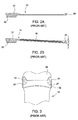
- Figure 2A schematically illustrates a partial sectional side view of the end effector 14 without a substrate.
- Figure 2B is a schematic sectional side view of the end effector 14 with a substrate 30 loaded thereon. An increased droop in the end effector 14 is shown due to weight of the substrate 30 positioned on the end effector 14. After the substrate 30 is loaded, the free end droops to an angle ⁇ .
- FIG. 3 schematically illustrates a top view of the end effector 14 secured on the mounting interface 28 of the arm assembly 16.
- the fixed end 27 of the end effector 14 is snuggly fitted between sidewalls 31 of the mounting interface 28 to prevent any rotations.
- the present invention generally relates to apparatus and methods for transfer a substrate at high temperatures. Particularly, embodiments of the present invention relates to high temperature anti-droop end effectors for transferring semiconductor substrates.
- One embodiment of the present invention provides an end effector for using with a substrate handler comprising a free end having a substrate supporting plane configured to support a substrate and positioned that substrate at a first angle relative to a horizontal plane, and a fixed end configured to be mounted to the substrate handler, wherein the end effector is mounted to the substrate handler at a position that the substrate supporting plane is at a second angle relative to the horizontal plane when no substrate is disposed on the free end, and the first angle is different from the second angle.
- Another embodiment of the present invention provides an end effector for using with a substrate handler comprising a free end having a substrate supporting plane configured to support a substrate thereon, and a fixed end having a bottom plane configured to secure the fixed end on a mounting surface of the substrate handler, wherein the bottom plane is formed at an angle relative to the substrate supporting plane.
- a substrate handler comprising a motion arm having a mounting plate, and an end effector configured to support a substrate
- the end effector comprises a free end having a substrate supporting plane configured to support the substrate at a first angle relative to a horizontal plane, and a fixed end mounted to the mounting plate of the motion arm, wherein the end effector is mounted to the mounting plate at a position that the substrate supporting surface is at a second angle relative to the horizontal plane when no substrate is disposed on the free end, and the first angle is different from the second angle.
- Embodiments are also directed to apparatuses for carrying out the disclosed methods and including apparatus parts for performing described method steps. Furthermore, embodiments are also directed to methods by which the described apparatus operates or by which the described apparatus is manufactured. It may include method steps for carrying out functions of the apparatus or manufacturing parts of the apparatus. The method steps may be performed by way of hardware components, firmware, software, a computer programmed by appropriate software, by any combination thereof or in any other manner.
- Figure 1 schematically illustrates a substrate handler configured for handling substrates in a transfer chamber.
- Figures 2A-B (prior art) schematically illustrate partial sectional side views of a drooping end effector.
- Figure 3 schematically illustrates a top view of an end effector that deforms at high temperature.
- Figure 4 schematically illustrates an exploded view of an end effector assembly in accordance with one embodiment of the present invention.
- Figures 5A-B schematically illustrate sectional side views of the end effector assembly of Figure 4 .
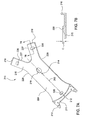
- Figure 6 schematically illustrates a partial top view of the end effector assembly of Figure 4 .
- FIGS 7A-B schematically illustrates an end effector in accordance with one embodiment of the present invention.
- the present invention generally relates apparatus and method for transferring semiconductor substrates.
- Embodiments of the present invention provide an end effector with anti-drooping and high temperature capabilities.
- an end effector may be mounted at a predetermined angle to counteract drooping caused by weight of the substrate and/or the end effector itself.
- a slope is formed on a mounting end of the end effector to facilitate an angled mounting.
- an end effector is mounted to a robot arm with side tolerance to allow thermal expansion.
- an end effector is secured to a robot arm near a center of a fixed end of the end effector.
- a clamp is used to secure an end effector to a robot arm.
- Embodiments of the present invention relate to high temperature anti-droop end effectors for transferring semiconductor substrates.
- One embodiment of the present invention provides an end effector for using with a substrate handler.
- the end effector comprises a free end having a substrate supporting plane configured to support a substrate and positioned that substrate at a first angle relative to a horizontal plane.
- the end effector comprises a fixed end configured to be mounted to the substrate handler, wherein the end effector is mounted to the substrate handler at a position that the substrate supporting plane is at a second angle relative to the horizontal plane when no substrate is disposed on the free end, and the first angle is different from the second angle.
- FIG. 4 schematically illustrates an exploded view of an end effector assembly 100 in accordance with one embodiment of the present invention.
- the end effector assembly 100 comprises an end effector 110 and a clamp 130 configured to secured the end effector 110 in a cavity 141 of a mounting plate 140 of a robot arm.
- the mounting plate 140, the end effector 110 and the clamp 130 are stacked together using screws 133 through corresponding holes 143, 113, 131.
- the end effector 110 has a free end 124 and a fixed end 111 configured for mounting the end effector 110 to the mounting plate 140.
- the fixed end 111 and the clamp 130 have similar shape of the cavity 141 so that both the fixed end 111 and the clamp 130 sit in the cavity 141.
- the free end 124 has two fingers 115 defined by outer opposing edges 128 and inner facing edges 127.
- the end effector 110 has a substrate sensing cutout 118 at a standard location for permitting a sensor beam, such as an infrared beam, to detect the presence a substrate on the end effector 110.
- the end effector 110 also has a center-finder hole 114. An operator may open a chamber and insert a pin into the center-finder hole 114 to calibrate the center of the end effector 110, so that the end effector 110 may be properly aligned with the chamber when dropping off or picking up a substrate in the chamber.
- the outer opposing edges 128 curve in a unique hour glass shape starting with the fixed end 111 of the end effector 110 and then taper out to form recesses.
- the inner facing edges 127 curve together to form a recess that extends into the area of the substrate sensing cutout 118.
- the recesses in the end effector 110 limit the mass of the end effector 110 to achieve lightweight and strong support for a substrate.
- the end effector 110 has a shelf 125 formed near the fixed end 111, and shelves 126 formed near tips of the fingers 115.
- the shelves 125, 126 are configured to support a backside of a substrate and provide clearance for the backside of the substrate above the level of the main part of the free end 124.
- the shelves 125, 126 form a substrate supporting surface 125a configured to support the backside of the substrate.
- the end effector 110 also has end shoes 117, 116 configured for laterally containing a substrate therein.
- the end effector 110 is mounted at a predetermined angle to counteract drooping.
- Figures 5A-B schematically illustrate sectional side views of the end effector assembly of Figure 4 .
- the end effector 110 is "sandwiched" between the mounting plate 140 and the clamp 130.
- Dashed line 150 indicates a desired angle that a substrate is to be handled on the end effector 110.
- the desired angle is about zero degree, i.e. parallel, to a horizontal plane.
- the end effector 110 is mounted such that the substrate supporting surface 125a is at a predetermined angle ⁇ relative to the desired angle marked by the dashed line 150.
- the predetermined angle ⁇ is determined to compensate drooping of the end effector 110 due to the weight of a substrate so that when the substrate is positioned on the end effector 110, the substrate is parallel to the dashed line 150.
- Factors effect the predetermined angle ⁇ may comprise weight and size of the substrate, properties of the material of the end effector 110, structure of the end effector 110, and a temperature at which the substrate is to be transferred.
- the angled mounting shown in Figure 5A may be achieved by forming a slope at a bottom surface 119 of the fixed end 111.
- the bottom surface 119 of the fixed end 111 may be sloped so that the bottom surface 119 and the substrate supporting surface 125a are not parallel.
- the bottom surface 119 extends to a bottom plane 119b.
- the substrate supporting surface 125a extends to a supporting plane 125b.
- the bottom plane 119b intersects the supporting plane 125b.
- a sloping angle y which is defined between the bottom plane 119a and an original bottom surface 119a, may be determined corresponding to the angle ⁇ .
- the fixed end 111 may have a tapered shape with a top surface 120 parallel to the supporting plane 125b and the original bottom plane 119a, and the bottom surface 119 forms an angle of ⁇ with the top surface 120.
- the angle ⁇ may be determined by a displacement of the free end 124 when a substrate is positioned thereon.
- the end effector 110 may be formed first without a slope on the bottom surface 119 and mounted on the mounting plate 140 so that the fixed end 111 is mounted substantially horizontal in a processing environment. Then a substrate can be positioned on the free end 124 and a total displacement of the free end 124 from the horizontal plane may be measured. The slope angle ⁇ may be determined to correct the total displacement.
- end effectors of the present invention may be custom built with slopes of different angle ⁇ for different process parameters, such as processing temperature, weight and size of substrates being processed, material and structure of the end effector.
- a substrate handler such as a robot, may avoid drooping at different processes by using different end effectors.
- a slope may be formed on a top surface of the mounting plate 140 to mount the end effector 110 in a predetermined angle.
- the mounting plate 140 may be positioned in a predetermined angle on the robot arm so that the end effector mounted on the mounting plate 140 is angled.
- alignment between an end effector and a mounting plate of a substrate handler may be obtained using constraints near a center of a mounting region of the end effector.
- alignment of the end effector 110 may be achieved using an aligning notch 112 formed near a central line 152 of the fixed end 111.
- a centering hole 132 on the clamp 130 is aligned with a centering hole 142 formed on the mounting plate 140.
- a dowel pin 121 is used to thread the centering hole 132 of the clamp 130, the aligning notch 112 of the end effector 110, and the centering hole 142 of the mounting plate 140 when the end effector 110 is mounted.
- Figure 6 schematically illustrates a top view of the end effector assembly 100 of Figure 4 without the clamp 130. Because the alignment is obtained using the aligning notch 112 and the dowel pin 121, relief seams 122 may be made between side walls 144 of the mounting plate 140 and the fixed end 111 of the end effector 110. The relief seams 122 and the aligning notch 112 formed near the center of the fixed end 111 allow the fixed end 111 of the end effector 110 to expand inside the cavity 141 without distortion. This is particularly useful when the end effector 110 is made of a material with greater thermal expansion rate than the material of the mounting plate 140 and/or the clamp 130.
- End effectors of the present invention may be made from any suitable material that compatible with semiconductor processes to be performed in corresponding processing chambers.
- the end effector is made from aluminum.
- the end effector may be made with nickel plated aluminum.
- Other suitable materials may include titanium, stainless steel, and ceramic.
- the clamp may be made from suitable materials such as titanium, aluminum, stainless steel and ceramic.
- the clamp 130 and the mounting plate 140 may be made from the same material so that the clamp 130 may be snuggly fitted in the cavity 141 of the mounting plate 140.
- an end effector is made from aluminum, while a clamp for mounting the end effector in a mounting plate is made from titanium.
- Figures 7A-B schematically illustrates an end effector 210 in accordance with another embodiment of the present invention.
- the end effector 210 having a free end 224 and a fixed end 211 configured for mounting the end effector 210 to a mounting plate.
- the fixed end 211 is similar to the fixed end 111 of the end effector 110 and may be mounted in a similar way.
- the fixed end 211 has an aligning notch 212 formed near a central line 252 of the end effector 210, and a plurality of through holes 213 for mounting screws.
- the free end 224 has two fingers 215 defined by outer opposing edges 228 and inner facing edges 227.
- the end effector 210 has a substrate sensing hole 218 at a standard location for permitting a sensor beam, such as an infrared beam, to detect the presence a substrate on the end effector 210.
- the end effector 210 also has a center-finder hole 214. An operator may open the chamber and insert a pin into the center-finder hole 214 to calibrate the center of the end effector 210, so that the end effector 210 may be properly aligned with dropping off or picking up a substrate in the chamber.
- the outer opposing edges 228 are substantially linear near the center portion forming a relatively robust free end 224, which provides stable support to a substrate.
- the end effector 210 has three bump supports 226 formed on the free end 224.
- the three bump supports 226 form a three-point substrate support configuration for minimum contact with a substrate.
- the bump supports 226 may be machined on the free end 224 to provide clearance for an edge of the substrate from the free end 224.
- the end effector 210 also has end shoes 216 forming a circle larger than a substrate being transferred. The end shoes 216 are configured for laterally catching a substrate therein in emergency.
- the bump supports 226 and the end shoes 216 may be formed with rounded corners to avoid scratching the substrate, thus, reducing particle contamination.
Landscapes
- Engineering & Computer Science (AREA)
- Robotics (AREA)
- Mechanical Engineering (AREA)
- Container, Conveyance, Adherence, Positioning, Of Wafer (AREA)
- Manipulator (AREA)
Abstract
Description
- Embodiments of the present invention generally relate to handling and transfer semiconductor substrates during semiconductor processing. More particularly, embodiments of the present invention relate to end effectors for use with a robot for handling semiconductor substrates.
- The use of robot arms is a well established manufacturing expedient in applications where human handling is inadequate and/or undesired. For example, in the semiconductor manufacturing, robot arms are used to handle substrates during and between various steps to provide speed and reduce contamination.
- A substrate handler used in semiconductor processing generally includes one or more end effectors, also known as a robot blade or a carrier, attached to a robot arm. The end effectors are configured to support a substrate during substrate transferring. For an integrated semiconductor processing system, a robot arm is generally disposed in a transfer chamber having facets to accommodate a plurality of processing chambers, and loading/unloading ports. During processing, the robot arm in the transfer chamber first loads a substrate to the end effector from a loading port. After retrieving the substrate to the transfer chamber, the robot arm feeds the substrate to a processing chamber connected to the transfer chamber. The robot arm drops the substrate on a substrate support in the processing chamber and retrieves the end effector. When the process is completed in the processing chamber, the robot arm is employed to retrieve the substrate from the substrate chamber and to shuttle the substrate to another processing chamber for the next processing step.
- Some common transfer chambers have facets to accommodate four to six processing chambers. The processing chambers may include rapid thermal processing (RTP) chambers, physical vapor deposition (PVD) chambers, chemical vapor deposition (CVD) chambers, and etch chambers.
-
Figure 1 schematically illustrates asubstrate handler 10 configured for handling substrates in a transfer chamber. Thesubstrate handler 10 includes twoend effectors 14 attached to anarm assembly 16 attached to a rotatingportion 18. During transferring, a substrate sits on theend effector 14. Theend effector 14 has a fixedend 27 attached to amounting interface 28 of thearm assembly 16, and afree end 29 configured to support a substrate thereon. Thefree end 29 may have asubstrate sensing hole 15 configured to let through a sensor beam used to detect presence of a substrate. Thearm assembly 16 moves theend effectors 14 radially outward from and inward to thesubstrate handler 10 to insert a substrate into or retrieve a substrate from a processing chamber. - The end effectors of prior art have several limitations. First, the end effector exhibits a droop (i.e. a tip-to-tail deflection) due to natural material compliance and weight of the substrate. Droop becomes more pronounced as the end effector becomes thinner to access densely packed substrates and as the size of the substrates become larger.
Figure 2A schematically illustrates a partial sectional side view of theend effector 14 without a substrate.Figure 2B is a schematic sectional side view of theend effector 14 with asubstrate 30 loaded thereon. An increased droop in theend effector 14 is shown due to weight of thesubstrate 30 positioned on theend effector 14. After thesubstrate 30 is loaded, the free end droops to an angle α. - High precision is critical in semiconductor processing. It is critical for a substrate handler, therefore, an end effector, to have high precision alignment. The end effectors are generally aligned and tightly secured on the robot arm to prevent any unwanted moves, which may cause distortion due to thermal expansion. During some high temperature processes, such as rapid thermal annealing, the end effector may need to transfer a hot substrate or to operate in a hot chamber. The temperature may be up to 350°C. The tightly secured end effector may become deformed due to thermal expansion at such high temperature.
Figure 3 schematically illustrates a top view of theend effector 14 secured on themounting interface 28 of thearm assembly 16. The fixedend 27 of theend effector 14 is snuggly fitted betweensidewalls 31 of themounting interface 28 to prevent any rotations. When theend effector 14 is made from material having a larger thermal expansion rate than the material of themounting interface 28, the fixedend 27 of theend effector 14 may exhaust any tolerance inseams 32 and become deformed. Additionally, drooping also increases at higher temperature. - Therefore, there is a need for apparatus and methods for transfer a substrate at high temperature without drooping or otherwise deforming.
- The present invention generally relates to apparatus and methods for transfer a substrate at high temperatures. Particularly, embodiments of the present invention relates to high temperature anti-droop end effectors for transferring semiconductor substrates.
- One embodiment of the present invention provides an end effector for using with a substrate handler comprising a free end having a substrate supporting plane configured to support a substrate and positioned that substrate at a first angle relative to a horizontal plane, and a fixed end configured to be mounted to the substrate handler, wherein the end effector is mounted to the substrate handler at a position that the substrate supporting plane is at a second angle relative to the horizontal plane when no substrate is disposed on the free end, and the first angle is different from the second angle.
- Another embodiment of the present invention provides an end effector for using with a substrate handler comprising a free end having a substrate supporting plane configured to support a substrate thereon, and a fixed end having a bottom plane configured to secure the fixed end on a mounting surface of the substrate handler, wherein the bottom plane is formed at an angle relative to the substrate supporting plane.
- Yet another embodiment of the present invention provides a substrate handler comprising a motion arm having a mounting plate, and an end effector configured to support a substrate, wherein the end effector comprises a free end having a substrate supporting plane configured to support the substrate at a first angle relative to a horizontal plane, and a fixed end mounted to the mounting plate of the motion arm, wherein the end effector is mounted to the mounting plate at a position that the substrate supporting surface is at a second angle relative to the horizontal plane when no substrate is disposed on the free end, and the first angle is different from the second angle.
- Embodiments are also directed to apparatuses for carrying out the disclosed methods and including apparatus parts for performing described method steps. Furthermore, embodiments are also directed to methods by which the described apparatus operates or by which the described apparatus is manufactured. It may include method steps for carrying out functions of the apparatus or manufacturing parts of the apparatus. The method steps may be performed by way of hardware components, firmware, software, a computer programmed by appropriate software, by any combination thereof or in any other manner.
- Further advantages, features, aspects and details are evident from the dependent claims, the description and the drawings.
- So that the manner in which the above recited features of the present invention can be understood in detail, a more particular description of the invention, briefly summarized above, may be had by reference to embodiments, some of which are illustrated in the appended drawings. It is to be noted, however, that the appended drawings illustrate only typical embodiments of this invention and are therefore not to be considered limiting of its scope, for the invention may admit to other equally effective embodiments.
- The accompanying drawings relate to embodiments of the invention and are described in the following:
-
Figure 1 (prior art) schematically illustrates a substrate handler configured for handling substrates in a transfer chamber. -
Figures 2A-B (prior art) schematically illustrate partial sectional side views of a drooping end effector. -
Figure 3 (prior art) schematically illustrates a top view of an end effector that deforms at high temperature. -
Figure 4 schematically illustrates an exploded view of an end effector assembly in accordance with one embodiment of the present invention. -
Figures 5A-B schematically illustrate sectional side views of the end effector assembly ofFigure 4 . -
Figure 6 schematically illustrates a partial top view of the end effector assembly ofFigure 4 . -
Figures 7A-B schematically illustrates an end effector in accordance with one embodiment of the present invention. - To facilitate understanding, identical reference numerals have been used, where possible, to designate identical elements that are common to the figures. It is contemplated that elements disclosed in one embodiment may be beneficially utilized on other embodiments without specific recitation.
- The present invention generally relates apparatus and method for transferring semiconductor substrates. Embodiments of the present invention provide an end effector with anti-drooping and high temperature capabilities. In one embodiment of the present invention, an end effector may be mounted at a predetermined angle to counteract drooping caused by weight of the substrate and/or the end effector itself. In one embodiment, a slope is formed on a mounting end of the end effector to facilitate an angled mounting. In one embodiment of the present invention, an end effector is mounted to a robot arm with side tolerance to allow thermal expansion. In one embodiment, an end effector is secured to a robot arm near a center of a fixed end of the end effector. In one embodiment of the present invention, a clamp is used to secure an end effector to a robot arm.
- Embodiments of the present invention relate to high temperature anti-droop end effectors for transferring semiconductor substrates. One embodiment of the present invention provides an end effector for using with a substrate handler. The end effector comprises a free end having a substrate supporting plane configured to support a substrate and positioned that substrate at a first angle relative to a horizontal plane. The end effector comprises a fixed end configured to be mounted to the substrate handler, wherein the end effector is mounted to the substrate handler at a position that the substrate supporting plane is at a second angle relative to the horizontal plane when no substrate is disposed on the free end, and the first angle is different from the second angle.
-
Figure 4 schematically illustrates an exploded view of anend effector assembly 100 in accordance with one embodiment of the present invention. Theend effector assembly 100 comprises anend effector 110 and aclamp 130 configured to secured theend effector 110 in acavity 141 of a mountingplate 140 of a robot arm. In one embodiment, the mountingplate 140, theend effector 110 and theclamp 130 are stacked together usingscrews 133 throughcorresponding holes - The
end effector 110 has afree end 124 and afixed end 111 configured for mounting theend effector 110 to the mountingplate 140. Thefixed end 111 and theclamp 130 have similar shape of thecavity 141 so that both thefixed end 111 and theclamp 130 sit in thecavity 141. - The
free end 124 has twofingers 115 defined by outer opposingedges 128 and inner facing edges 127. Theend effector 110 has asubstrate sensing cutout 118 at a standard location for permitting a sensor beam, such as an infrared beam, to detect the presence a substrate on theend effector 110. Theend effector 110 also has a center-finder hole 114. An operator may open a chamber and insert a pin into the center-finder hole 114 to calibrate the center of theend effector 110, so that theend effector 110 may be properly aligned with the chamber when dropping off or picking up a substrate in the chamber. - The outer opposing
edges 128 curve in a unique hour glass shape starting with thefixed end 111 of theend effector 110 and then taper out to form recesses. The inner facing edges 127 curve together to form a recess that extends into the area of thesubstrate sensing cutout 118. The recesses in theend effector 110 limit the mass of theend effector 110 to achieve lightweight and strong support for a substrate. - The
end effector 110 has ashelf 125 formed near thefixed end 111, andshelves 126 formed near tips of thefingers 115. Theshelves free end 124. Theshelves substrate supporting surface 125a configured to support the backside of the substrate. Theend effector 110 also hasend shoes - In one embodiment of the present invention, the
end effector 110 is mounted at a predetermined angle to counteract drooping.Figures 5A-B schematically illustrate sectional side views of the end effector assembly ofFigure 4 . - As shown in
Figure 5A , theend effector 110 is "sandwiched" between the mountingplate 140 and theclamp 130. Dashedline 150 indicates a desired angle that a substrate is to be handled on theend effector 110. Usually, the desired angle is about zero degree, i.e. parallel, to a horizontal plane. In one embodiment, theend effector 110 is mounted such that thesubstrate supporting surface 125a is at a predetermined angle β relative to the desired angle marked by the dashedline 150. In one embodiment, the predetermined angle β is determined to compensate drooping of theend effector 110 due to the weight of a substrate so that when the substrate is positioned on theend effector 110, the substrate is parallel to the dashedline 150. Factors effect the predetermined angle β may comprise weight and size of the substrate, properties of the material of theend effector 110, structure of theend effector 110, and a temperature at which the substrate is to be transferred. - In one embodiment, the angled mounting shown in
Figure 5A may be achieved by forming a slope at abottom surface 119 of thefixed end 111. As shown inFigure 5B , thebottom surface 119 of thefixed end 111 may be sloped so that thebottom surface 119 and thesubstrate supporting surface 125a are not parallel. As shown inFigure 5B , thebottom surface 119 extends to abottom plane 119b. Thesubstrate supporting surface 125a extends to a supportingplane 125b. Thebottom plane 119b intersects the supportingplane 125b. A sloping angle y, which is defined between thebottom plane 119a and anoriginal bottom surface 119a, may be determined corresponding to the angle β. In one embodiment, thefixed end 111 may have a tapered shape with atop surface 120 parallel to the supportingplane 125b and theoriginal bottom plane 119a, and thebottom surface 119 forms an angle of γ with thetop surface 120. - In one embodiment, the angle γ may be determined by a displacement of the
free end 124 when a substrate is positioned thereon. For example, theend effector 110 may be formed first without a slope on thebottom surface 119 and mounted on the mountingplate 140 so that thefixed end 111 is mounted substantially horizontal in a processing environment. Then a substrate can be positioned on thefree end 124 and a total displacement of thefree end 124 from the horizontal plane may be measured. The slope angle γ may be determined to correct the total displacement. - As such, end effectors of the present invention may be custom built with slopes of different angle γ for different process parameters, such as processing temperature, weight and size of substrates being processed, material and structure of the end effector. A substrate handler, such as a robot, may avoid drooping at different processes by using different end effectors.
- In another embodiment, a slope may be formed on a top surface of the mounting
plate 140 to mount theend effector 110 in a predetermined angle. In another embodiment, the mountingplate 140 may be positioned in a predetermined angle on the robot arm so that the end effector mounted on the mountingplate 140 is angled. - In one embodiment of the present invention, alignment between an end effector and a mounting plate of a substrate handler may be obtained using constraints near a center of a mounting region of the end effector. Referring back to
Figure 4 , alignment of theend effector 110 may be achieved using an aligningnotch 112 formed near acentral line 152 of thefixed end 111. A centeringhole 132 on theclamp 130 is aligned with a centeringhole 142 formed on the mountingplate 140. Adowel pin 121 is used to thread the centeringhole 132 of theclamp 130, the aligningnotch 112 of theend effector 110, and the centeringhole 142 of the mountingplate 140 when theend effector 110 is mounted. -
Figure 6 schematically illustrates a top view of theend effector assembly 100 ofFigure 4 without theclamp 130. Because the alignment is obtained using the aligningnotch 112 and thedowel pin 121,relief seams 122 may be made betweenside walls 144 of the mountingplate 140 and thefixed end 111 of theend effector 110. The relief seams 122 and the aligningnotch 112 formed near the center of thefixed end 111 allow thefixed end 111 of theend effector 110 to expand inside thecavity 141 without distortion. This is particularly useful when theend effector 110 is made of a material with greater thermal expansion rate than the material of the mountingplate 140 and/or theclamp 130. - Even though, a dowel pin and a notch alignment is described in accordance with the present invention, other suitable alignment methods aligning an end effector near a center region of a fixed end is also contemplated.
- End effectors of the present invention may be made from any suitable material that compatible with semiconductor processes to be performed in corresponding processing chambers. In one embodiment, the end effector is made from aluminum. In another embodiment, the end effector may be made with nickel plated aluminum. Other suitable materials may include titanium, stainless steel, and ceramic. Similarly, the clamp may be made from suitable materials such as titanium, aluminum, stainless steel and ceramic.
- In one embodiment, the
clamp 130 and the mountingplate 140 may be made from the same material so that theclamp 130 may be snuggly fitted in thecavity 141 of the mountingplate 140. - In one embodiment, an end effector is made from aluminum, while a clamp for mounting the end effector in a mounting plate is made from titanium.
-
Figures 7A-B schematically illustrates anend effector 210 in accordance with another embodiment of the present invention. - The
end effector 210 having afree end 224 and afixed end 211 configured for mounting theend effector 210 to a mounting plate. Thefixed end 211 is similar to thefixed end 111 of theend effector 110 and may be mounted in a similar way. Thefixed end 211 has an aligningnotch 212 formed near acentral line 252 of theend effector 210, and a plurality of throughholes 213 for mounting screws. - The
free end 224 has twofingers 215 defined by outer opposingedges 228 and inner facing edges 227. Theend effector 210 has asubstrate sensing hole 218 at a standard location for permitting a sensor beam, such as an infrared beam, to detect the presence a substrate on theend effector 210. Theend effector 210 also has a center-finder hole 214. An operator may open the chamber and insert a pin into the center-finder hole 214 to calibrate the center of theend effector 210, so that theend effector 210 may be properly aligned with dropping off or picking up a substrate in the chamber. - The outer opposing
edges 228 are substantially linear near the center portion forming a relatively robustfree end 224, which provides stable support to a substrate. - The
end effector 210 has three bump supports 226 formed on thefree end 224. The three bump supports 226 form a three-point substrate support configuration for minimum contact with a substrate. The bump supports 226 may be machined on thefree end 224 to provide clearance for an edge of the substrate from thefree end 224. Theend effector 210 also hasend shoes 216 forming a circle larger than a substrate being transferred. The end shoes 216 are configured for laterally catching a substrate therein in emergency. - As shown in
Figure 7B , the bump supports 226 and the end shoes 216 may be formed with rounded corners to avoid scratching the substrate, thus, reducing particle contamination. - While the foregoing is directed to embodiments of the present invention, other and further embodiments of the invention may be devised without departing from the basic scope thereof, and the scope thereof is determined by the claims that follow.
Claims (15)
- An end effector for using with a substrate handler, comprising:a free end (124; 224) having a substrate supporting plane configured to support a substrate and positioned that substrate at a first angle relative to a horizontal plane; anda fixed end (111; 211) configured to be mounted to the substrate handler, wherein the end effector (110; 210) is mounted to the substrate handler at a position that the substrate supporting plane is at a second angle relative to the horizontal plane when no substrate is disposed on the free end (124; 224), and the first angle is different from the second angle.
- The end effector of claim 1, the difference between the first angle and the second angle is predetermined by structure of the end effector (110; 210), material of the end effector (110; 210), size and weight of the substrate, or operating temperature.
- The end effector of claim 1 or 2, wherein the fixed end (111; 211) has a top surface substantially parallel to the substrate supporting plane of the free end (124; 224), and a bottom surface having a slope relative to the top surface.
- The end effector of claim 3, wherein a degree of the slope is corresponding to the difference between the first angle and the second angle.
- The end effector of any of claims 1 to 4, wherein the free end (124; 224) comprises three supporting bumps configured to support the substrate thereon without contacting an edge of the substrate.
- The end effector of any of claims 1 to 5, wherein the fixed end (111; 211) has an aligning notch (112; 212) near a central line of the end effector (110; 210), and the aligning notch (112; 212) is configured to align the end effector (110; 210) with the substrate handler.
- An end effector for using with a substrate handler, comprising:a free end (124; 224) having a substrate supporting surface configured to support a substrate thereon, wherein the substrate supporting surface extends to a first plane; anda fixed end (111; 211) having a mounting surface configured to secure the end effector (110; 210) against the substrate handler, wherein the mounting surface extends to a second plane, and the first plane intersects the second plane.
- The end effector of claim 7, wherein the fixed end (111; 211) has an aligning notch (112; 212) formed near the central line of the end effector (110; 210) fixed configured to align the end effector (110; 210) with the substrate handler.
- The end effector of claim 7 or 8, wherein the fixed end (111; 211) is configured to be disposed in a mounting cavity of a mounting plate of the substrate handler with allowance to accommodate thermal expansion difference between the mounting plate and the end effector (110; 210), and the fixed end (111; 211) is aligned to the mounting plate by inserting a dowel pin through an aligning notch (112; 212) formed near the central line of the end effector (110; 210) and a centering hole formed in the mounting plate.
- A substrate handler, comprising:a motion arm having a mounting plate; andan end effector (110; 210) configured to support a substrate, wherein the end effector (110; 210) comprises:a free end (124; 224) having a substrate supporting plane configured to support the substrate at a first angle relative to a horizontal plane; anda fixed end (111; 211) mounted to the mounting plate of the motion arm, wherein the end effector (110; 210) is mounted to the mounting plate at a position that the substrate supporting surface is at a second angle relative to the horizontal plane when no substrate is disposed on the free end (124; 224), and the first angle is different from the second angle.
- The substrate handler of claim 10, further comprising a clamp member configured to mount the end effector (110; 210) on the mounting plate, wherein the end effector (110; 210) is stacked between the clamp member and the mounting plate.
- The substrate handler of claim 10 or 11, wherein the fixed end (111; 211) has an aligning notch (112; 212) formed near a central line of the end effector (110; 210), the aligning notch (112; 212) is configured to align the end effector (110; 210) with the mounting plate.
- The substrate handler of any of claims 10 to 12, wherein the mounting plate has a mounting plane configured to receive a bottom surface of the end effector (110; 210), the mounting plane is disposed horizontally, and the bottom surface is sloped relative to the substrate supporting plane.
- The substrate handler of any of claims 10 to 13, wherein the mounting plate has a mounting plane configured to receive a bottom surface of the end effector (110; 210), the mounting plane is sloped relative to a horizontal plane, and the bottom surface is parallel to the substrate supporting plane.
- The substrate handler of any of claims 10 to 14, the end effector (110; 210) is made of aluminum and the mounting plate is made of titanium.
Applications Claiming Priority (1)
| Application Number | Priority Date | Filing Date | Title |
|---|---|---|---|
| US89409807P | 2007-03-09 | 2007-03-09 |
Publications (3)
| Publication Number | Publication Date |
|---|---|
| EP1968110A2 true EP1968110A2 (en) | 2008-09-10 |
| EP1968110A3 EP1968110A3 (en) | 2013-12-04 |
| EP1968110B1 EP1968110B1 (en) | 2020-09-23 |
Family
ID=39493366
Family Applications (1)
| Application Number | Title | Priority Date | Filing Date |
|---|---|---|---|
| EP08152541.2A Active EP1968110B1 (en) | 2007-03-09 | 2008-03-10 | High temperature anti-droop end effector for substrate transfer |
Country Status (7)
| Country | Link |
|---|---|
| US (1) | US9443752B2 (en) |
| EP (1) | EP1968110B1 (en) |
| JP (1) | JP5800447B2 (en) |
| KR (1) | KR100989721B1 (en) |
| CN (1) | CN101303994B (en) |
| SG (1) | SG146547A1 (en) |
| TW (1) | TWI455226B (en) |
Cited By (1)
| Publication number | Priority date | Publication date | Assignee | Title |
|---|---|---|---|---|
| US12540041B2 (en) | 2021-09-17 | 2026-02-03 | Asm Ip Holding B.V. | End effector and substrate processing apparatus including end effector |
Families Citing this family (13)
| Publication number | Priority date | Publication date | Assignee | Title |
|---|---|---|---|---|
| US11831462B2 (en) | 2007-08-24 | 2023-11-28 | Icontrol Networks, Inc. | Controlling data routing in premises management systems |
| CN104658958B (en) * | 2015-02-13 | 2018-04-24 | 苏州工业园区纳米产业技术研究院有限公司 | Wafer grabbing arm |
| CN106032014A (en) * | 2015-03-13 | 2016-10-19 | 上海理想万里晖薄膜设备有限公司 | Mechanical arm |
| CN105575865A (en) * | 2015-12-23 | 2016-05-11 | 苏州工业园区纳米产业技术研究院有限公司 | Structural transformation of deep silicon machine arm for slices after deep silicon etching process and transformation method thereof |
| US10090188B2 (en) * | 2016-05-05 | 2018-10-02 | Applied Materials, Inc. | Robot subassemblies, end effector assemblies, and methods with reduced cracking |
| US10651067B2 (en) * | 2017-01-26 | 2020-05-12 | Brooks Automation, Inc. | Method and apparatus for substrate transport apparatus position compensation |
| US20190013215A1 (en) * | 2017-07-05 | 2019-01-10 | Kawasaki Jukogyo Kabushiki Kaisha | Substrate holding hand and substrate conveying apparatus including the same |
| CN109461693B (en) | 2017-09-06 | 2023-06-02 | 台湾积体电路制造股份有限公司 | Wafer transfer device, wafer processing system and method |
| US11011397B2 (en) * | 2018-12-20 | 2021-05-18 | Axcelis Technologies, Inc. | Wafer soak temperature readback and control via thermocouple embedded end effector for semiconductor processing equipment |
| KR102322129B1 (en) | 2019-06-07 | 2021-11-04 | 블루테크코리아 주식회사 | End effector for semiconductor robot |
| US12334375B2 (en) | 2019-08-08 | 2025-06-17 | Lam Research Corporation | Spindle assembly for wafer transfer in a multi-station process module |
| US12575377B2 (en) * | 2023-03-01 | 2026-03-10 | Applied Materials, Inc. | Method and tool for restricting substrate a support bead inside an opening formed in a substrate support |
| KR102876268B1 (en) * | 2024-08-30 | 2025-10-28 | 주식회사 원익아이피에스 | Substrate transfer apparatus and substrate processing apparatus |
Family Cites Families (29)
| Publication number | Priority date | Publication date | Assignee | Title |
|---|---|---|---|---|
| JPH0661331A (en) * | 1992-08-06 | 1994-03-04 | Tokyo Electron Tohoku Ltd | Substrate transfer system |
| JP3172900B2 (en) | 1993-02-19 | 2001-06-04 | 東京エレクトロン株式会社 | Substrate transfer apparatus, substrate processing apparatus, substrate transfer method and substrate processing method |
| JP3125908B2 (en) * | 1993-09-14 | 2001-01-22 | 株式会社安川電機 | Manufacturing method of wafer transfer fork |
| JPH0799225A (en) * | 1993-09-27 | 1995-04-11 | Dainippon Screen Mfg Co Ltd | Substrate conveyer |
| US5957651A (en) | 1995-06-08 | 1999-09-28 | Kokusai Electric Co., Ltd. | Substrate carrying apparatus |
| US6267423B1 (en) | 1995-12-08 | 2001-07-31 | Applied Materials, Inc. | End effector for semiconductor wafer transfer device and method of moving a wafer with an end effector |
| US5746460A (en) * | 1995-12-08 | 1998-05-05 | Applied Materials, Inc. | End effector for semiconductor wafer transfer device and method of moving a wafer with an end effector |
| JPH10177999A (en) | 1996-10-15 | 1998-06-30 | Ebara Corp | Substrate-transporting hand and polishing device |
| DE69732157T2 (en) | 1996-02-28 | 2005-12-29 | Ebara Corp. | Transport robot with drip water protection |
| JPH10242235A (en) * | 1997-02-27 | 1998-09-11 | Dainippon Screen Mfg Co Ltd | Substrate carrier |
| CN1291345A (en) * | 1998-02-18 | 2001-04-11 | 应用材料有限公司 | End effectors for use on processing system wafer handlers |
| US6489741B1 (en) | 1998-08-25 | 2002-12-03 | Genmark Automation, Inc. | Robot motion compensation system |
| JP2000183128A (en) * | 1998-12-17 | 2000-06-30 | Komatsu Ltd | Control device for work transfer device |
| JP4189093B2 (en) * | 1999-08-31 | 2008-12-03 | 京セラ株式会社 | Ceramic transfer arm and method for manufacturing the same |
| US7334826B2 (en) * | 2001-07-13 | 2008-02-26 | Semitool, Inc. | End-effectors for handling microelectronic wafers |
| US7289230B2 (en) * | 2002-02-06 | 2007-10-30 | Cyberoptics Semiconductors, Inc. | Wireless substrate-like sensor |
| JP2004128021A (en) | 2002-09-30 | 2004-04-22 | Mitsubishi Electric Corp | Wafer transfer device |
| TWI356100B (en) * | 2003-07-24 | 2012-01-11 | Applied Materials Inc | Shutter disk and blade for physical vapor depositi |
| US7433756B2 (en) * | 2003-11-13 | 2008-10-07 | Applied Materials, Inc. | Calibration of high speed loader to substrate transport system |
| JP4696467B2 (en) * | 2004-04-19 | 2011-06-08 | 三菱樹脂株式会社 | Robot arm device hand |
| KR20050108944A (en) * | 2004-05-14 | 2005-11-17 | 삼성전자주식회사 | Wafer transfer |
| US20060216137A1 (en) | 2004-07-02 | 2006-09-28 | Katsunori Sakata | Carrying apparatus and carrying control method for sheet-like substrate |
| TW200618964A (en) | 2004-10-14 | 2006-06-16 | Toshiba Machine Co Ltd | Industrial robot |
| JP2006110662A (en) * | 2004-10-14 | 2006-04-27 | Toshiba Mach Co Ltd | Industrial robot |
| US20060113806A1 (en) * | 2004-11-29 | 2006-06-01 | Asm Japan K.K. | Wafer transfer mechanism |
| KR101198179B1 (en) * | 2005-01-17 | 2012-11-16 | 삼성전자주식회사 | Method for compensation static deflection of handling robot and apparatus thereof |
| JP2006332460A (en) * | 2005-05-27 | 2006-12-07 | Hitachi High-Tech Control Systems Corp | Wafer transfer device |
| JP4903027B2 (en) * | 2006-01-06 | 2012-03-21 | 東京エレクトロン株式会社 | Substrate transport device and substrate support |
| US7717481B2 (en) * | 2007-01-11 | 2010-05-18 | Applied Materials, Inc. | High temperature robot end effector |
-
2008
- 2008-03-07 TW TW097108171A patent/TWI455226B/en active
- 2008-03-07 CN CN2008100074550A patent/CN101303994B/en active Active
- 2008-03-07 US US12/044,401 patent/US9443752B2/en active Active
- 2008-03-07 SG SG200801902-8A patent/SG146547A1/en unknown
- 2008-03-07 KR KR1020080021358A patent/KR100989721B1/en active Active
- 2008-03-07 JP JP2008057723A patent/JP5800447B2/en active Active
- 2008-03-10 EP EP08152541.2A patent/EP1968110B1/en active Active
Cited By (1)
| Publication number | Priority date | Publication date | Assignee | Title |
|---|---|---|---|---|
| US12540041B2 (en) | 2021-09-17 | 2026-02-03 | Asm Ip Holding B.V. | End effector and substrate processing apparatus including end effector |
Also Published As
| Publication number | Publication date |
|---|---|
| EP1968110A3 (en) | 2013-12-04 |
| US20080219815A1 (en) | 2008-09-11 |
| JP5800447B2 (en) | 2015-10-28 |
| CN101303994B (en) | 2011-05-18 |
| JP2008227491A (en) | 2008-09-25 |
| KR100989721B1 (en) | 2010-10-26 |
| TW200845267A (en) | 2008-11-16 |
| US9443752B2 (en) | 2016-09-13 |
| TWI455226B (en) | 2014-10-01 |
| KR20080082922A (en) | 2008-09-12 |
| EP1968110B1 (en) | 2020-09-23 |
| SG146547A1 (en) | 2008-10-30 |
| CN101303994A (en) | 2008-11-12 |
Similar Documents
| Publication | Publication Date | Title |
|---|---|---|
| EP1968110A2 (en) | High temperature anti-droop end effector for substrate transfer | |
| US7661544B2 (en) | Semiconductor wafer boat for batch processing | |
| TWI527149B (en) | Inertial wafer centering end effector and conveying device | |
| JP4404481B2 (en) | Vacuum processing system, wafer handler and end effector | |
| US10325799B2 (en) | Dual temperature heater | |
| JP5268126B2 (en) | Dual robot transfer system | |
| EP0884769A1 (en) | Heat-treating boat for semiconductor wafer | |
| CN110062818A (en) | Wafer positioning pedestal for semiconductor processing | |
| US10504762B2 (en) | Bridging front opening unified pod (FOUP) | |
| US8752872B2 (en) | Edge grip end effector | |
| KR102497963B1 (en) | Substrate Handling Equipment for Wafers | |
| US20190259635A1 (en) | Process kit for processing reduced sized substrates | |
| US20190259647A1 (en) | Deposition ring for processing reduced size substrates | |
| CN111656506A (en) | Equipment for processing substrates of various sizes | |
| US20230249360A1 (en) | Robotic end effector equipped with replaceable wafer contact pads | |
| JP2025542150A (en) | Carrier with anti-rotation function | |
| TW202501671A (en) | Wafer handling assembly, semiconductor processing apparatus, and wafer processing method |
Legal Events
| Date | Code | Title | Description |
|---|---|---|---|
| PUAI | Public reference made under article 153(3) epc to a published international application that has entered the european phase |
Free format text: ORIGINAL CODE: 0009012 |
|
| AK | Designated contracting states |
Kind code of ref document: A2 Designated state(s): AT BE BG CH CY CZ DE DK EE ES FI FR GB GR HR HU IE IS IT LI LT LU LV MC MT NL NO PL PT RO SE SI SK TR |
|
| AX | Request for extension of the european patent |
Extension state: AL BA MK RS |
|
| RIC1 | Information provided on ipc code assigned before grant |
Ipc: H01L 21/677 20060101ALI20130705BHEP Ipc: H01L 21/687 20060101AFI20130705BHEP |
|
| PUAL | Search report despatched |
Free format text: ORIGINAL CODE: 0009013 |
|
| AK | Designated contracting states |
Kind code of ref document: A3 Designated state(s): AT BE BG CH CY CZ DE DK EE ES FI FR GB GR HR HU IE IS IT LI LT LU LV MC MT NL NO PL PT RO SE SI SK TR |
|
| AX | Request for extension of the european patent |
Extension state: AL BA MK RS |
|
| RIC1 | Information provided on ipc code assigned before grant |
Ipc: H01L 21/677 20060101ALI20131025BHEP Ipc: H01L 21/687 20060101AFI20131025BHEP |
|
| 17P | Request for examination filed |
Effective date: 20140218 |
|
| RBV | Designated contracting states (corrected) |
Designated state(s): AT BE BG CH CY CZ DE DK EE ES FI FR GB GR HR HU IE IS IT LI LT LU LV MC MT NL NO PL PT RO SE SI SK TR |
|
| AKX | Designation fees paid |
Designated state(s): AT BE BG CH CY CZ DE DK EE ES FI FR GB GR HR HU IE IS IT LI LT LU LV MC MT NL NO PL PT RO SE SI SK TR |
|
| 17Q | First examination report despatched |
Effective date: 20160616 |
|
| STAA | Information on the status of an ep patent application or granted ep patent |
Free format text: STATUS: EXAMINATION IS IN PROGRESS |
|
| GRAP | Despatch of communication of intention to grant a patent |
Free format text: ORIGINAL CODE: EPIDOSNIGR1 |
|
| STAA | Information on the status of an ep patent application or granted ep patent |
Free format text: STATUS: GRANT OF PATENT IS INTENDED |
|
| INTG | Intention to grant announced |
Effective date: 20191212 |
|
| GRAJ | Information related to disapproval of communication of intention to grant by the applicant or resumption of examination proceedings by the epo deleted |
Free format text: ORIGINAL CODE: EPIDOSDIGR1 |
|
| STAA | Information on the status of an ep patent application or granted ep patent |
Free format text: STATUS: EXAMINATION IS IN PROGRESS |
|
| GRAP | Despatch of communication of intention to grant a patent |
Free format text: ORIGINAL CODE: EPIDOSNIGR1 |
|
| STAA | Information on the status of an ep patent application or granted ep patent |
Free format text: STATUS: GRANT OF PATENT IS INTENDED |
|
| INTC | Intention to grant announced (deleted) | ||
| INTG | Intention to grant announced |
Effective date: 20200417 |
|
| GRAS | Grant fee paid |
Free format text: ORIGINAL CODE: EPIDOSNIGR3 |
|
| GRAA | (expected) grant |
Free format text: ORIGINAL CODE: 0009210 |
|
| STAA | Information on the status of an ep patent application or granted ep patent |
Free format text: STATUS: THE PATENT HAS BEEN GRANTED |
|
| AK | Designated contracting states |
Kind code of ref document: B1 Designated state(s): AT BE BG CH CY CZ DE DK EE ES FI FR GB GR HR HU IE IS IT LI LT LU LV MC MT NL NO PL PT RO SE SI SK TR |
|
| REG | Reference to a national code |
Ref country code: GB Ref legal event code: FG4D |
|
| REG | Reference to a national code |
Ref country code: CH Ref legal event code: EP |
|
| REG | Reference to a national code |
Ref country code: DE Ref legal event code: R096 Ref document number: 602008063284 Country of ref document: DE |
|
| REG | Reference to a national code |
Ref country code: IE Ref legal event code: FG4D |
|
| REG | Reference to a national code |
Ref country code: AT Ref legal event code: REF Ref document number: 1317239 Country of ref document: AT Kind code of ref document: T Effective date: 20201015 |
|
| PG25 | Lapsed in a contracting state [announced via postgrant information from national office to epo] |
Ref country code: BG Free format text: LAPSE BECAUSE OF FAILURE TO SUBMIT A TRANSLATION OF THE DESCRIPTION OR TO PAY THE FEE WITHIN THE PRESCRIBED TIME-LIMIT Effective date: 20201223 Ref country code: NO Free format text: LAPSE BECAUSE OF FAILURE TO SUBMIT A TRANSLATION OF THE DESCRIPTION OR TO PAY THE FEE WITHIN THE PRESCRIBED TIME-LIMIT Effective date: 20201223 Ref country code: HR Free format text: LAPSE BECAUSE OF FAILURE TO SUBMIT A TRANSLATION OF THE DESCRIPTION OR TO PAY THE FEE WITHIN THE PRESCRIBED TIME-LIMIT Effective date: 20200923 Ref country code: SE Free format text: LAPSE BECAUSE OF FAILURE TO SUBMIT A TRANSLATION OF THE DESCRIPTION OR TO PAY THE FEE WITHIN THE PRESCRIBED TIME-LIMIT Effective date: 20200923 Ref country code: FI Free format text: LAPSE BECAUSE OF FAILURE TO SUBMIT A TRANSLATION OF THE DESCRIPTION OR TO PAY THE FEE WITHIN THE PRESCRIBED TIME-LIMIT Effective date: 20200923 Ref country code: GR Free format text: LAPSE BECAUSE OF FAILURE TO SUBMIT A TRANSLATION OF THE DESCRIPTION OR TO PAY THE FEE WITHIN THE PRESCRIBED TIME-LIMIT Effective date: 20201224 |
|
| REG | Reference to a national code |
Ref country code: AT Ref legal event code: MK05 Ref document number: 1317239 Country of ref document: AT Kind code of ref document: T Effective date: 20200923 |
|
| PG25 | Lapsed in a contracting state [announced via postgrant information from national office to epo] |
Ref country code: LV Free format text: LAPSE BECAUSE OF FAILURE TO SUBMIT A TRANSLATION OF THE DESCRIPTION OR TO PAY THE FEE WITHIN THE PRESCRIBED TIME-LIMIT Effective date: 20200923 |
|
| REG | Reference to a national code |
Ref country code: NL Ref legal event code: MP Effective date: 20200923 |
|
| REG | Reference to a national code |
Ref country code: LT Ref legal event code: MG4D |
|
| PG25 | Lapsed in a contracting state [announced via postgrant information from national office to epo] |
Ref country code: NL Free format text: LAPSE BECAUSE OF FAILURE TO SUBMIT A TRANSLATION OF THE DESCRIPTION OR TO PAY THE FEE WITHIN THE PRESCRIBED TIME-LIMIT Effective date: 20200923 Ref country code: LT Free format text: LAPSE BECAUSE OF FAILURE TO SUBMIT A TRANSLATION OF THE DESCRIPTION OR TO PAY THE FEE WITHIN THE PRESCRIBED TIME-LIMIT Effective date: 20200923 Ref country code: PT Free format text: LAPSE BECAUSE OF FAILURE TO SUBMIT A TRANSLATION OF THE DESCRIPTION OR TO PAY THE FEE WITHIN THE PRESCRIBED TIME-LIMIT Effective date: 20210125 Ref country code: RO Free format text: LAPSE BECAUSE OF FAILURE TO SUBMIT A TRANSLATION OF THE DESCRIPTION OR TO PAY THE FEE WITHIN THE PRESCRIBED TIME-LIMIT Effective date: 20200923 Ref country code: EE Free format text: LAPSE BECAUSE OF FAILURE TO SUBMIT A TRANSLATION OF THE DESCRIPTION OR TO PAY THE FEE WITHIN THE PRESCRIBED TIME-LIMIT Effective date: 20200923 Ref country code: CZ Free format text: LAPSE BECAUSE OF FAILURE TO SUBMIT A TRANSLATION OF THE DESCRIPTION OR TO PAY THE FEE WITHIN THE PRESCRIBED TIME-LIMIT Effective date: 20200923 |
|
| PG25 | Lapsed in a contracting state [announced via postgrant information from national office to epo] |
Ref country code: PL Free format text: LAPSE BECAUSE OF FAILURE TO SUBMIT A TRANSLATION OF THE DESCRIPTION OR TO PAY THE FEE WITHIN THE PRESCRIBED TIME-LIMIT Effective date: 20200923 Ref country code: AT Free format text: LAPSE BECAUSE OF FAILURE TO SUBMIT A TRANSLATION OF THE DESCRIPTION OR TO PAY THE FEE WITHIN THE PRESCRIBED TIME-LIMIT Effective date: 20200923 Ref country code: IS Free format text: LAPSE BECAUSE OF FAILURE TO SUBMIT A TRANSLATION OF THE DESCRIPTION OR TO PAY THE FEE WITHIN THE PRESCRIBED TIME-LIMIT Effective date: 20210123 Ref country code: ES Free format text: LAPSE BECAUSE OF FAILURE TO SUBMIT A TRANSLATION OF THE DESCRIPTION OR TO PAY THE FEE WITHIN THE PRESCRIBED TIME-LIMIT Effective date: 20200923 |
|
| REG | Reference to a national code |
Ref country code: DE Ref legal event code: R097 Ref document number: 602008063284 Country of ref document: DE |
|
| PG25 | Lapsed in a contracting state [announced via postgrant information from national office to epo] |
Ref country code: SK Free format text: LAPSE BECAUSE OF FAILURE TO SUBMIT A TRANSLATION OF THE DESCRIPTION OR TO PAY THE FEE WITHIN THE PRESCRIBED TIME-LIMIT Effective date: 20200923 |
|
| PLBE | No opposition filed within time limit |
Free format text: ORIGINAL CODE: 0009261 |
|
| STAA | Information on the status of an ep patent application or granted ep patent |
Free format text: STATUS: NO OPPOSITION FILED WITHIN TIME LIMIT |
|
| PG25 | Lapsed in a contracting state [announced via postgrant information from national office to epo] |
Ref country code: SI Free format text: LAPSE BECAUSE OF FAILURE TO SUBMIT A TRANSLATION OF THE DESCRIPTION OR TO PAY THE FEE WITHIN THE PRESCRIBED TIME-LIMIT Effective date: 20200923 Ref country code: DK Free format text: LAPSE BECAUSE OF FAILURE TO SUBMIT A TRANSLATION OF THE DESCRIPTION OR TO PAY THE FEE WITHIN THE PRESCRIBED TIME-LIMIT Effective date: 20200923 |
|
| 26N | No opposition filed |
Effective date: 20210624 |
|
| PG25 | Lapsed in a contracting state [announced via postgrant information from national office to epo] |
Ref country code: IT Free format text: LAPSE BECAUSE OF FAILURE TO SUBMIT A TRANSLATION OF THE DESCRIPTION OR TO PAY THE FEE WITHIN THE PRESCRIBED TIME-LIMIT Effective date: 20200923 Ref country code: MC Free format text: LAPSE BECAUSE OF FAILURE TO SUBMIT A TRANSLATION OF THE DESCRIPTION OR TO PAY THE FEE WITHIN THE PRESCRIBED TIME-LIMIT Effective date: 20200923 |
|
| REG | Reference to a national code |
Ref country code: CH Ref legal event code: PL |
|
| GBPC | Gb: european patent ceased through non-payment of renewal fee |
Effective date: 20210310 |
|
| PG25 | Lapsed in a contracting state [announced via postgrant information from national office to epo] |
Ref country code: LI Free format text: LAPSE BECAUSE OF NON-PAYMENT OF DUE FEES Effective date: 20210331 Ref country code: LU Free format text: LAPSE BECAUSE OF NON-PAYMENT OF DUE FEES Effective date: 20210310 Ref country code: CH Free format text: LAPSE BECAUSE OF NON-PAYMENT OF DUE FEES Effective date: 20210331 Ref country code: IE Free format text: LAPSE BECAUSE OF NON-PAYMENT OF DUE FEES Effective date: 20210310 Ref country code: GB Free format text: LAPSE BECAUSE OF NON-PAYMENT OF DUE FEES Effective date: 20210310 |
|
| PG25 | Lapsed in a contracting state [announced via postgrant information from national office to epo] |
Ref country code: HU Free format text: LAPSE BECAUSE OF FAILURE TO SUBMIT A TRANSLATION OF THE DESCRIPTION OR TO PAY THE FEE WITHIN THE PRESCRIBED TIME-LIMIT; INVALID AB INITIO Effective date: 20080310 Ref country code: CY Free format text: LAPSE BECAUSE OF FAILURE TO SUBMIT A TRANSLATION OF THE DESCRIPTION OR TO PAY THE FEE WITHIN THE PRESCRIBED TIME-LIMIT Effective date: 20200923 |
|
| PG25 | Lapsed in a contracting state [announced via postgrant information from national office to epo] |
Ref country code: TR Free format text: LAPSE BECAUSE OF FAILURE TO SUBMIT A TRANSLATION OF THE DESCRIPTION OR TO PAY THE FEE WITHIN THE PRESCRIBED TIME-LIMIT Effective date: 20200923 |
|
| PG25 | Lapsed in a contracting state [announced via postgrant information from national office to epo] |
Ref country code: MT Free format text: LAPSE BECAUSE OF FAILURE TO SUBMIT A TRANSLATION OF THE DESCRIPTION OR TO PAY THE FEE WITHIN THE PRESCRIBED TIME-LIMIT Effective date: 20200923 |
|
| REG | Reference to a national code |
Ref country code: DE Ref legal event code: R079 Ref document number: 602008063284 Country of ref document: DE Free format text: PREVIOUS MAIN CLASS: H01L0021687000 Ipc: H10P0072760000 |
|
| PGFP | Annual fee paid to national office [announced via postgrant information from national office to epo] |
Ref country code: FR Payment date: 20251015 Year of fee payment: 19 |
|
| PGFP | Annual fee paid to national office [announced via postgrant information from national office to epo] |
Ref country code: BE Payment date: 20251015 Year of fee payment: 19 |
|
| PGFP | Annual fee paid to national office [announced via postgrant information from national office to epo] |
Ref country code: DE Payment date: 20251015 Year of fee payment: 19 |