EP1964266B1 - Verfahren zum multizyklus-takt-gating - Google Patents
Verfahren zum multizyklus-takt-gating Download PDFInfo
- Publication number
- EP1964266B1 EP1964266B1 EP06819558A EP06819558A EP1964266B1 EP 1964266 B1 EP1964266 B1 EP 1964266B1 EP 06819558 A EP06819558 A EP 06819558A EP 06819558 A EP06819558 A EP 06819558A EP 1964266 B1 EP1964266 B1 EP 1964266B1
- Authority
- EP
- European Patent Office
- Prior art keywords
- gating
- data latching
- group
- latching devices
- circuit
- Prior art date
- Legal status (The legal status is an assumption and is not a legal conclusion. Google has not performed a legal analysis and makes no representation as to the accuracy of the status listed.)
- Not-in-force
Links
Images



Classifications
-
- H—ELECTRICITY
- H03—ELECTRONIC CIRCUITRY
- H03K—PULSE TECHNIQUE
- H03K19/00—Logic circuits, i.e. having at least two inputs acting on one output; Inverting circuits
-
- G—PHYSICS
- G06—COMPUTING OR CALCULATING; COUNTING
- G06F—ELECTRIC DIGITAL DATA PROCESSING
- G06F30/00—Computer-aided design [CAD]
- G06F30/30—Circuit design
Definitions
- the present invention relates to circuit design generally and in particular to clock gating of data latching devices.
- Complicated pieces of hardware typically comprise millions of transistors. Circuit designers typically utilize computer-aided design programs to aid their design process. Once a designer has finished the conceptual design of a circuit, there are many optimizations which can be made.
- FIG. 1A shows a first circuit 10 having a flip-flop 12. Like all flip-flops, flip-flop 12 is controlled by a clock signal CLK. When clock signal CLK goes high, flip-flop 12 puts out a value Q calculated from its input I, which may be a function of a logic circuit 14, which, in turn, may be a function of a plurality of inputs (a, b and c are shown). Flip-flop 12 will perform the calculation, irrespective of whether or not input I has changed.
- a circuit designer when coming to determine how to minimize the power consumption of his circuit, may review the activities of the flip-flops and may "gate" those which he knows will not change value given a particular situation. To do so, the designer may add circuitry to disconnect the clock input to the flip-flop.
- Fig. 1B This change is shown in Fig. 1B .
- flip-flop 12 In the circuit, now labeled 10', flip-flop 12 remains as does logic circuit 14, but the clock signal to flip-flop 12 has changed.
- the clock signal, labeled GCLK is now a gated clock signal which is only active when both clock signal CLK and an enable signal EN are active.
- Gated clock signal GCLK is generated with a gate 16. Clock-gating performed like this on an individual flip-flop is known as "fine-grained" clock gating.
- clock-gating Another method for clock-gating is known as "coarse-grained" clock gating. Under coarse-grained clock gating, a large number of flip-flops are shut off using the same clock gating function, thus providing a significant reduction in power usage. For example, sections of a circuit which operate as a single unit, such as a floating point unit, may be clock-gated.
- clock gating saves little, if any, power.
- a unit which has a multi-cycle clock gater and a circuit design updater.
- the multi-cycle clock gater may generate multi-cycle gating groups of data latching devices of a circuit design.
- the circuit design updater may update the circuit design with selected multi-cycle gating groups.
- each gating group may be associated with a single gating function.
- data latching devices of 0 th level of the gating group may be gated with the gating function and the ith level data latching devices of the gating function may be gated with ith latched versions of the gating function.
- the data latching devices may be flip-flops or latches.
- the multi-cycle clock gater includes an indicator signal generator, an unfolder and a gating function determiner.
- the indicator signal generator may create indicator signals identifying conditions under which the values of data latching devices of an input circuit design do not change.
- the unfolder may unfold the circuit with the indicator signals a plurality K of times and the gating function determiner may determine a plurality of candidate gating functions for the multiplicity of data latching devices from at least the unfolded indicator signals.
- the gating function determiner includes a binary decision diagram operator to build a binary decision diagram (BDD) X of the unfolded indicator signals ANDed together, to generate a BDD Y of X at a no change value and, for each time stamp k, to remove variables of a BDD Y k whose input is not from the kth cycle.
- BDD binary decision diagram
- the multi-cycle clock gater includes a circuit reviewer, a gating function determiner and a group generator.
- the circuit reviewer may find a group G of data latching devices of the circuit that depend only on an input cycle.
- the gating function determiner may determine a group H j of the data latching devices of the group G which share a jth gating function F j and the group generator may add, for each group H j , the data latching devices of the circuit which receive input from existing data latching devices of group H j .
- the group generator includes a level 0 definer to define, for each initial group H j , the data latching devices therein as level 0 data latching devices and a non-level 0 definer to add, for each ith level, a data latching device of the circuit to group H j as a level i+1 data latching device if the data latching device depends only on a level i data latching device already present in group H j .
- the present invention incorporates the methods implemented by the multi-cycle clock gater and the circuit design updater.
- clock gating function for a particular flip-flop may be used in a latched form as the clock gating function for at least one other flip-flop.
- This may be known as "multi-cycle" clock gating because it may involve multiple cycles of flip-flops using the same, possibly latched, clock gating function.
- the multi-cycle gating groups may also gate "data dependent" states of data latching devices, where a data dependent state may be defined as a state when the output of the data latching device depends on the data input values, and not only on the values of the control inputs.
- Fig. 2 illustrates a power reducing, circuit reviewer 18.
- Reviewer 18 may comprise a novel, multi-cycle clock gater 20 and a circuit updater 22.
- Multi-cycle clock gater 20 may review an input circuit design R to find potential, multi-cycle, clock gating opportunities and to generate logic functions to control the clocked gates.
- Circuit updater 22 may interact with a user, such as a circuit designer, to determine which potential opportunities the user wants to implement and may update circuit design R with the selected clock gates and their associated logic. The result may be an updated, lower power design R'.
- Multi-cycle clock gater 20 may generate clock-gating logic functions which may be used for multiple cycles, thus reducing the overhead and/or allowing bigger functions (i.e. with more gates) to be used for clock gating.
- Multi-cycle clock gater 20 may operate by considering the circuit as a whole, without dividing the circuit into multiple units based on their operation. Reference is now made to Fig. 3 , which illustrates the method performed by clock gater 20, and to Figs. 4A, 4B and 4C , which are useful in understanding the steps of the method of Fig. 3 .
- clock gater 20 may review design R to identify (step 24) the flip-flops, latches or other data latching devices therein.
- the remaining discussion will use the term "flip-flop", since such are shown in Figs. 4 .
- the present invention is operative for all types of data latching devices.
- clock gater 20 may determine which enable signals control which flip-flops and may group the flip-flops accordingly. It will be appreciated that not all flip-flops may be controlled by enable signals and that not all enable signals may be utilized for gating. Some enable signals may control flip-flops having feedback loops therearound. Such enable signals may be converted to different enable signals using the method described in US Patent Application Serial No. 11/295936 "Clock Gating Through Data Independent Logic", filed December 7, 2005 published under US 2007/0130549 on 07.06.2007.
- clock gater 20 may then temporarily add logic (step 26) which may identify conditions under which the value of either flip-flops in the circuit that are enabled by the current enable signal, or of flip-flops not assigned to any of the enable signals, do not change.
- Fig. 4A shows a circuit 30 to be analyzed. It has five inputs x1, x2, x3, x4 and x5 and three flip-flops FF-1, FF-2 and FF-3.
- Fig. 4B shows the circuit, here labeled 30', after the addition of temporary logic 34-1, 34-2 and 34-3 associated with flip-flops FF-1, FF-2 and FF-3, respectively.
- the output signal of XOR 34-i may be an indicator signal pi and may have a value of 1 when the input A and output B of its associated flip-flop FF-i are different and a value of 0 when they are the same.
- indicator signal pi may indicate when flip-flop FF-i changes value and when it does not.
- Clock gater 20 may add the extra logic 34-i (i.e. the XORs in the example of Fig. 4B ) into the RTL logic description.
- clock gater 20 may "unfold" circuit 30' for K steps, where K is the depth of the logic of interest.
- K might be defined as the number of flip-flops in the longest path from chip input to chip output, or from the input to a section of the chip to its output.
- K might be 2, since there are only two levels of flip-flops (FF-1 and FF-3 at the first level and FF-2 at the second level).
- Unfolding may be the process of virtually making a copy of circuit 30' for each time k.
- the article by R. Tzoref, M. Matusevich, E. Berger, I. Beer, entitled “An Optimized Symbolic Bounded Model Checking Engine”, given at CHARME 2003 discusses the unfolding process within a symbolic model checker.
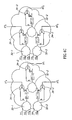
- Fig. 4C shows the unfolding for the exemplary circuit 30' for two cycles 1 and 2.
- Each input signal xj is time-stamped as are the indicator signals pi.
- Fig. 4C has two copies of input signal x1 (x1 1 , x1 2 ) for the two cycles 1 and 2 and there are two copies of indicator signal p3 (p3 1 , p3 2 ).
- clock gater 20 may then build (step 42) a binary decision diagram (BDD) X that represents the unfolded indicator signals P i k ANDed together.
- a binary decision diagram (BDD) is a generally compact representation of a Boolean expression and is commonly used in symbolic model checking, particularly of complicated hardware.
- a BDD is a directed acyclic graph that represents a Boolean expression.
- Fig. 5 shows an exemplary BDD for the expression ((A & B & C)
- Each circle (or node) indicates a variable (A, B, C, D) and the lines indicate the directions to follow when the variable evaluates FALSE (on the left) or TRUE (on the right).
- Leaf nodes 51 represent the value of the Boolean expressions.
- clock gater 20 may utilize the RTL logic of amended circuit 30' to determine the Boolean expressions Q i defining each indicator signal pi. Since Boolean operations may be performed on a BDD, clock gater 20 may AND together all of the Boolean expressions Q i and their multiple copies Q i k to generate the BDD X.
- clock gater 20 may generate a no-change BDD having the value that indicator signals pi generate when flip-flops FF-i do not change values.
- clock gater 20 may determine a kth gating group by eliminating any indicator signal p i that depends on inputs x j k from cycles other than k. To do so, clock gater 20 may first generate (step 52) a temporary copy Y k of no change BDD Y for use in cycle k. Clock gater 20 may then remove (step 54) from temporary no change BDD Y k any indicator signals p i(not_k) which are functions of inputs x j not _k from cycles other than k. The remaining indicator signals pi(remain) form a kth candidate gating group Y k '.
- Clock gater 20 may remove the undesirable signals p i(not_k) and may then perform standard compaction operations on BDD Y k '. Such operations are known in the art and are discussed in the article by R. Bryant entitled “Graph-based algorithms for Boolean function manipulation", IEEE Transactions on Computers, Vol. C-35(8), 1986 .
- the remaining indicator signals p i(remain) that are left in kth candidate gating group Y k ' indicate the flip-flops FF-i that may be gated with the current enable signal and/or its latched form.
- Gating groups which are large compared to the logic required to implement their gating function may be good candidates for clock gating.
- the size of a gating group may be defined by the number of flip-flops or other data latching devices therein.
- clock gater 20 may have a set of candidate gating functions and their gating groups for review.
- Circuit updater 22 may provide these gating functions and their gating groups to the circuit designer who, in turn, may select which ones to implement, after which circuit updater 22 may then add the selected gating functions to the circuit, thereby generating the updated circuit R'.
- Fig. 6A shows a simple circuit with 32 repetitions n of the same element
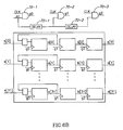
- Fig. 6B shows the clock gated version of the circuit.
- Each element n has an input s(n), a mux 60-n, and three concatenated flip-flops 62A-n, 62B-n and 62C-n.
- the outputs of flip-flop 62A-n, 62B-n and 62C-n are a (n), b(n) and o(n) and the input to mux 60-n is the input s(n), the signal en, and the output a(n) of flip-flop 62An.
- Muxes 60-n are enabled by an enable signal en.
- clock gater 20 may generate the following gating function, shown in Fig. 6B :
- the overhead is three gates 70-1, 70-2 and 70-3 and two delays 72-1 and 72-2. In certain cases, this might be an acceptable overhead. It will be appreciated that, even if there is combinational logic between the simple circuits (so that, for instance, b(0) might be a function of a(0) - a(4)), the above gating will work.
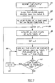
- FIG. 7 illustrates an alternative method, to be performed by clock gater 20, for determining which data latching devices to clock-gate for multi-cycle clock gating.
- clock gater 20 may initially review design R to identify (step 24) the data latching devices therein.
- step 24 the discussion below will use exemplary flip-flops, it being appreciated that all types of data latching devices are included.
- clock gater 20 may traverse (step 80) a netlist of design R to determine which flip-flops depend only on inputs. This is a set G.
- clock gater 20 may review the "input-only" flip-flops G, identified in the previous step, to determine which ones operate according to the same clock-gating function F j .
- Clock gating function F j may just be the enable functions to the input-only flip-flops G.
- clock-gating functions F j may be determined using standard algorithms for fine-grained clock-gating, such as that described in US Patent Application Serial No. 11/295936 "Clock Gating Through Data Independent Logic", filed December 7, 2005, mentioned hereinabove. The result may list the groups H j of data latching devices which may be clock gated together with the jth gating function F j .
- Clock gater 20 may then determine the flip-flops to be gated by each gating function F j . For each gating function F j , as controlled by a loop 84 over j, clock gater 20 may initialize (step 86) the flip-flops in gating group H j as "level 0" flip-flops. Clock gater 20 may then enter a loop 88 over i. In step 90, clock gater 20 may review the flip-flops of the circuit to find those which depend only on level i flip-flops in gating group H j . These flip-flops may be labeled "level i+1" flip-flops and may be added to gating group H j .
- clock gater 20 may check if any new flip-flops were added to gating group H j in step 90. If so, clock gater 20 may increment i, in step 94, and may continue in loop 88 until the result of step 92 is negative.
- clock gater 20 may generate the following gating function:
- each gating group H j may be the number of flip-flops stored therein.
Landscapes
- Engineering & Computer Science (AREA)
- Computer Hardware Design (AREA)
- Physics & Mathematics (AREA)
- Theoretical Computer Science (AREA)
- General Engineering & Computer Science (AREA)
- General Physics & Mathematics (AREA)
- Geometry (AREA)
- Evolutionary Computation (AREA)
- Computing Systems (AREA)
- Mathematical Physics (AREA)
- Design And Manufacture Of Integrated Circuits (AREA)
- Logic Circuits (AREA)
- Synchronisation In Digital Transmission Systems (AREA)
Claims (10)
- Verfahren zum Erzeugen von Multizyklus-Gattersteuerungsgruppen von Datenzwischenspeichereinheiten, wobei das Verfahren Folgendes umfasst:Erzeugen von Anzeigesignalen, die Bedingungen kennzeichnen, unter denen sich die Werte von einer Eingangsschaltkreisanordnung nicht ändern,K-faches Entfalten des Schaltkreises mit den Anzeigesignalen; undErmitteln einer Vielzahl von Kandidaten-Gattersteuerungsfunktionen für die Datenzwischenspeichereinheiten aus zumindest den entfalteten Anzeigesignalen; undwobei dieses Ermitteln Folgendes umfasst:Erstellen eines binären Entscheidungsdiagramms (binary decision diagram BDD) X aus den durch UND-Verknüpfung verbundenen, entfalteten Anzeigesignalen;Erzeugen eines BDD Y aus X bei sich nicht änderndem Wert; undfür jeden Zeitstempel k Entfernen von Variablen eines BDD Yk, deren Eingang nicht aus dem k-ten Zyklus stammt.
- Verfahren nach Anspruch 1, wobei jede der Gattersteuerungsgruppen mit einer einzigen Gattersteuerungsfunktion verknüpft ist und das Verfahren für jede Gattersteuerungsgruppe außerdem umfasst:Ansteuern von Datenzwischenspeichereinheiten der Gattersteuerungsgruppe der 0-ten Ebene mit der Gattersteuerungsfunktion und von Datenzwischenspeichereinheiten der Gattersteuerungsgruppe der i-ten Ebene mit einer i-ten zwischengespeicherten Version der Gattersteuerungsfunktion.
- Verfahren nach einem der vorangehenden Ansprüche, wobei das Erzeugen Folgendes umfasst:Suchen einer Gruppe G von Datenzwischenspeichervorrichtungen des Schaltkreises, die nur von einem Eingangszyklus abhängen,Ermitteln einer Gruppe Hj der Datenzwischenspeichereinheiten der Gruppe G, die eine j-te Gattersteuerungsfunktion Fj gemeinsam haben; undfür jede Gruppe Hj Hinzufügen der Datenzwischenspeichereinheiten des Schaltkreises, die Eingaben von in der Gruppe Hj enthaltenen Datenzwischenspeichereinheiten empfangen.
- Verfahren nach Anspruch 3, wobei das Hinzufügen Folgendes umfasst:für jede ursprüngliche Gruppe Hj Definieren der darin enthaltenen Datenzwischenspeichereinheiten als Datenzwischenspeichereinheiten der Ebene 0; undfür jede i-te Ebene Hinzufügen einer Datenzwischenspeichereinheit des Schaltkreises zu Gruppe Hj als Datenzwischenspeichereinheit der Ebene i+1, wenn die Datenzwischenspeichereinheit nur von einer bereits in Gruppe Hj enthaltenen Datenzwischenspeichereinheit der Ebene i abhängt.
- Taktgesteuerte Multizyklus-Logikschaltung zum Erzeugen von Multizyklus-Gattersteuerungsruppen von Datenzwischenspeichereinheiten, wobei die taktgesteuerte Multizyklus-Logikschaltung Folgendes umfasst:Eine Anzeigesignalerzeugungseinrichtung, um Anzeigesignale zu erzeugen, die Bedingungen anzeigen, unter denen sich die Werte von Datenzwischenspeichereinheiten einer Eingangsschaltkreisanordnung nicht ändern,eine Entfaltungseinrichtung, um den Schaltkreis mit den Anzeigesignalen K-mal zu entfalten; undeine Einrichtung zum Ermitteln von Gattersteuerungsfunktionen, um die Vielzahl von Kandidaten-Gattersteuerungsfunktionen für die Datenzwischenspeichereinheiten aus zumindest den entfalteten Anzeigesignalen zu ermitteln; undwobei die Einrichtung zum Ermitteln von Gattersteuerungsfunktionen Folgendes umfasst:einen Binäres-Entscheidungsdiagramm-Operator, um ein binäres Entscheidungsdiagramm (binary decision diagram BDD) X aus den durch UND-Verknüpfung verbundenen entfalteten Anzeigesignalen zu erstellen, um ein BDD Y aus X bei sich nicht änderndem Wert zu erzeugen, und um für jeden Zeitstempel k Variablen aus dem BDD zu entfernen, deren Eingang nicht aus dem k-ten Zyklus stammt.
- Taktgesteuerte Multizyklus-Logikschaltung nach Anspruch 5, der Folgendes umfasst:Eine Einrichtung zum Durchsuchen des Schaltkreises, um eine Gruppe G von Datenzwischenspeichereinheiten des Schaltkreises zu finden, die nur von einem Eingangszyklus abhängen,eine Einrichtung zum Ermitteln von Gattersteuerungsfunktionen, um eine Gruppe Hj der Datenzwischenspeichereinheiten der Gruppe G zu ermitteln, die eine j-te Gattersteuerungsfunktion Fj gemeinsam nutzen; undeine Einrichtung zum Erzeugen von Gruppen, um für jede Gruppe Hj die Datenzwischenspeichereinheiten des Schaltkreises hinzuzufügen, die eine Eingabe von in der Gruppe Hj enthaltenen Datenzwischenspeichereinheiten empfangen.
- Taktgesteuerte Multizyklus-Logikschaltung nach Anspruch 6, wobei die Einrichtung zum Erzeugen von Gruppen Folgendes umfasst:Eine Einrichtung, mit der eine Ebene 0 festgelegt wird, um für jede ursprüngliche Gruppe Hj die darin enthaltenen Datenzwischenspeichereinheiten als Datenzwischenspeichereinheiten der Ebene 0 festzulegen; undEine Einrichtung, damit eine Ebene 0 nicht festgelegt wird, um für jede i-te Ebene eine Datenzwischenspeichereinheit des Schaltkreises zur Gruppe Hj als Datenzwischenspeichereinheit der Ebene i+1 hinzuzufügen, wenn die Datenzwischenspeichereinheit nur von einer Datenzwischenspeichereinheit der Ebene i abhängt, die bereits in der Gruppe Hj enthalten ist.
- Taktgesteuerte Multizyklus-Logikschaltung nach einem der Ansprüche 5 bis 7, wobei jede der Gattersteuerungsgruppen mit einer einzigen Gattersteuerungsfunktion verknüpft ist und wobei die Einrichtung zum Aktualisieren des Schaltkreises eine Einrichtung zum Einsetzen von Gattersteuerungsfunktionen umfasst, um die Datenzwischenspeichereinheiten anzusteuern, wobei die Einrichtung zum Einsetzen von Gattersteuerungsfunktion für jede Gattersteuerungsgruppe Datenzwischenspeichereinheiten der Gattersteuerungsgruppe der 0-ten Ebene mit der Gattersteuerungsfunktion und Datenzwischenspeichereinheiten der Gattersteuerungsgruppe der i-ten Ebene mit einer i-ten gespeicherten Version der Gattersteuerungsfunktion ansteuert.
- Taktgesteuerte Multizyklus-Logikschaltung nach einem der Ansprüche 5 bis 8 und wobei die Datenzwischenspeichereinheiten Flip-Flops oder Zwischenspeicher (latches) sind.
- Vorrichtung, die Folgendes umfasst:eine Taktgesteuerte Multizyklus-Logikschaltung nach einem der Ansprüche 5 bis 9 zum multizyklischen Erzeugen von Multizyklus-Gattersteuerungsgruppen von Datenzwischenspeichereinheiten einer Schaltkreisanordnung; undeine Einrichtung zum Aktualisieren des Schaltkreises, um die Schaltkreisanordnung mit ausgewählten Multizyklus-Gattersteuerungsgruppen zu aktualisieren.
Applications Claiming Priority (2)
| Application Number | Priority Date | Filing Date | Title |
|---|---|---|---|
| US11/311,756 US7594200B2 (en) | 2005-12-19 | 2005-12-19 | Method for finding multi-cycle clock gating |
| PCT/EP2006/068582 WO2007071506A1 (en) | 2005-12-19 | 2006-11-16 | A method for multi-cycle clock gating |
Publications (2)
| Publication Number | Publication Date |
|---|---|
| EP1964266A1 EP1964266A1 (de) | 2008-09-03 |
| EP1964266B1 true EP1964266B1 (de) | 2009-03-11 |
Family
ID=37880745
Family Applications (1)
| Application Number | Title | Priority Date | Filing Date |
|---|---|---|---|
| EP06819558A Not-in-force EP1964266B1 (de) | 2005-12-19 | 2006-11-16 | Verfahren zum multizyklus-takt-gating |
Country Status (9)
| Country | Link |
|---|---|
| US (1) | US7594200B2 (de) |
| EP (1) | EP1964266B1 (de) |
| JP (1) | JP4988758B2 (de) |
| KR (1) | KR100992025B1 (de) |
| CN (1) | CN101341656B (de) |
| AT (1) | ATE425585T1 (de) |
| DE (1) | DE602006005714D1 (de) |
| TW (1) | TW200745891A (de) |
| WO (1) | WO2007071506A1 (de) |
Families Citing this family (17)
| Publication number | Priority date | Publication date | Assignee | Title |
|---|---|---|---|---|
| JP2008028930A (ja) * | 2006-07-25 | 2008-02-07 | Toshiba Corp | 半導体集積回路及びその設計方法 |
| US7882461B2 (en) | 2007-05-29 | 2011-02-01 | Magma Design Automation, Inc. | Method for optimized automatic clock gating |
| US7458050B1 (en) | 2008-03-21 | 2008-11-25 | International Business Machines Corporation | Methods to cluster boolean functions for clock gating |
| US7884649B1 (en) * | 2009-02-27 | 2011-02-08 | Magma Design Automation, Inc. | Selection of optimal clock gating elements |
| US8132144B2 (en) * | 2009-06-17 | 2012-03-06 | Oracle America, Inc. | Automatic clock-gating insertion and propagation technique |
| US8166444B2 (en) * | 2009-06-23 | 2012-04-24 | International Business Machines Corporations | Clock gating using abstraction refinement |
| JP5368941B2 (ja) * | 2009-11-06 | 2013-12-18 | シャープ株式会社 | 論理回路設計支援方法及び装置 |
| JP5494468B2 (ja) * | 2010-12-27 | 2014-05-14 | 富士通株式会社 | 状態検出装置、状態検出方法および状態検出のためのプログラム |
| KR20140020404A (ko) | 2012-08-08 | 2014-02-19 | 삼성전자주식회사 | 집적 회로의 소비 전력 모델링 방법 및 장치 |
| US8890573B2 (en) * | 2012-09-07 | 2014-11-18 | Nvidia Corporation | Clock gating latch, method of operation thereof and integrated circuit employing the same |
| US8656326B1 (en) * | 2013-02-13 | 2014-02-18 | Atrenta, Inc. | Sequential clock gating using net activity and XOR technique on semiconductor designs including already gated pipeline design |
| US10503856B2 (en) | 2013-12-05 | 2019-12-10 | International Business Machines Corporation | Phase algebra for specifying clocks and modes in hierarchical designs |
| US9268889B2 (en) | 2013-12-05 | 2016-02-23 | International Business Machines Corporation | Verification of asynchronous clock domain crossings |
| US10318695B2 (en) | 2013-12-05 | 2019-06-11 | International Business Machines Corporation | Phase algebra for virtual clock and mode extraction in hierarchical designs |
| US9916407B2 (en) | 2013-12-05 | 2018-03-13 | International Business Machines Corporation | Phase algebra for analysis of hierarchical designs |
| US10761559B2 (en) * | 2016-12-13 | 2020-09-01 | Qualcomm Incorporated | Clock gating enable generation |
| CN116959519B (zh) * | 2023-09-20 | 2023-12-15 | 深圳比特微电子科技有限公司 | 存储设备、包含该存储设备的片上系统和计算装置 |
Family Cites Families (16)
| Publication number | Priority date | Publication date | Assignee | Title |
|---|---|---|---|---|
| JPH03131976A (ja) * | 1989-10-18 | 1991-06-05 | Hitachi Ltd | 論理回路の製造方法 |
| US5980092A (en) * | 1996-11-19 | 1999-11-09 | Unisys Corporation | Method and apparatus for optimizing a gated clock structure using a standard optimization tool |
| US6247134B1 (en) * | 1999-03-31 | 2001-06-12 | Synopsys, Inc. | Method and system for pipe stage gating within an operating pipelined circuit for power savings |
| US6434704B1 (en) * | 1999-08-16 | 2002-08-13 | International Business Machines Corporation | Methods for improving the efficiency of clock gating within low power clock trees |
| US6785832B2 (en) * | 2001-06-22 | 2004-08-31 | International Business Machines Corporation | Process independent source synchronous data capture apparatus and method |
| JP2003330568A (ja) * | 2002-05-09 | 2003-11-21 | Toshiba Corp | 半導体集積回路および回路設計システム |
| GB0210625D0 (en) | 2002-05-09 | 2002-06-19 | Paradigm Design Systems | Control of guard flops |
| JP4083544B2 (ja) * | 2002-11-18 | 2008-04-30 | 富士通株式会社 | マルチサイクルパス解析方法 |
| JP4288066B2 (ja) * | 2002-12-27 | 2009-07-01 | エヌエックスピー ビー ヴィ | 回路装置 |
| GB0301244D0 (en) | 2003-01-20 | 2003-02-19 | Paradigm Design Systems Ltd | Improved clock gating for synchronous circuits |
| GB0301241D0 (en) * | 2003-01-20 | 2003-02-19 | Paradigm Design Systems Ltd | Clocked gating on measured performance |
| US7080334B2 (en) * | 2003-05-09 | 2006-07-18 | Incentia Design Systems Corp. | Automatic clock gating insertion in an IC design |
| US7032192B2 (en) * | 2003-05-22 | 2006-04-18 | Fujitsu Limited | Performing latch mapping of sequential circuits |
| US6844767B2 (en) * | 2003-06-18 | 2005-01-18 | Via-Cyrix, Inc. | Hierarchical clock gating circuit and method |
| US6983437B2 (en) * | 2003-11-05 | 2006-01-03 | Sun Microsystems, Inc. | Timing verification, automated multicycle generation and verification |
| JP2007164590A (ja) * | 2005-12-15 | 2007-06-28 | Fujitsu Ltd | 回路設計装置、回路設計プログラム、及び回路設計方法 |
-
2005
- 2005-12-19 US US11/311,756 patent/US7594200B2/en not_active Expired - Fee Related
-
2006
- 2006-11-16 JP JP2008546321A patent/JP4988758B2/ja not_active Expired - Fee Related
- 2006-11-16 EP EP06819558A patent/EP1964266B1/de not_active Not-in-force
- 2006-11-16 KR KR1020087015495A patent/KR100992025B1/ko not_active Expired - Fee Related
- 2006-11-16 WO PCT/EP2006/068582 patent/WO2007071506A1/en not_active Ceased
- 2006-11-16 CN CN2006800478040A patent/CN101341656B/zh active Active
- 2006-11-16 DE DE602006005714T patent/DE602006005714D1/de active Active
- 2006-11-16 AT AT06819558T patent/ATE425585T1/de not_active IP Right Cessation
- 2006-12-04 TW TW095144997A patent/TW200745891A/zh unknown
Also Published As
| Publication number | Publication date |
|---|---|
| DE602006005714D1 (de) | 2009-04-23 |
| EP1964266A1 (de) | 2008-09-03 |
| KR100992025B1 (ko) | 2010-11-05 |
| US20070157130A1 (en) | 2007-07-05 |
| CN101341656A (zh) | 2009-01-07 |
| JP4988758B2 (ja) | 2012-08-01 |
| US7594200B2 (en) | 2009-09-22 |
| WO2007071506A1 (en) | 2007-06-28 |
| KR20080077231A (ko) | 2008-08-21 |
| JP2009520287A (ja) | 2009-05-21 |
| ATE425585T1 (de) | 2009-03-15 |
| CN101341656B (zh) | 2010-09-22 |
| TW200745891A (en) | 2007-12-16 |
Similar Documents
| Publication | Publication Date | Title |
|---|---|---|
| EP1964266B1 (de) | Verfahren zum multizyklus-takt-gating | |
| Smith et al. | Optimization of NULL convention self-timed circuits | |
| US6301553B1 (en) | Method and apparatus for removing timing hazards in a circuit design | |
| CN115204076B (zh) | 集成电路的逻辑优化方法、装置、电子设备及可读介质 | |
| KR20090009915A (ko) | 동기 회로 설계 표현과 비동기 회로 설계 표현간의 자동 변환을 수행하기 위한 시스템 및 방법 | |
| US20080288901A1 (en) | Formally deriving a minimal clock-gating scheme | |
| Parsan et al. | Gate mapping automation for asynchronous NULL convention logic circuits | |
| US20080201671A1 (en) | Method for generating timing exceptions | |
| US20050268268A1 (en) | Methods and systems for structured ASIC electronic design automation | |
| US7484187B2 (en) | Clock-gating through data independent logic | |
| US6157903A (en) | Method of minimizing macrocell characterization time for state dependent power analysis | |
| Bingham et al. | Self-timed adaptive digit-serial addition | |
| Reese et al. | Introduction to logic synthesis using Verilog HDL | |
| US8245178B2 (en) | Method for multi-cycle clock gating | |
| Khodosevych et al. | Combining relaxation with NCL_X for enhanced optimization of asynchronous Null convention logic circuits | |
| Han et al. | Clocked and asynchronous FIFO characterization and comparison | |
| Gupta et al. | Acyclic modeling of combinational loops | |
| Blair | Verilog: accelerating digital design | |
| Lloyd et al. | Asynchronous microprocessors: From high level model to FPGA implementation | |
| Grout | Electronic circuit and system design using python and VHDL | |
| Zervas et al. | Generalized Low Power Design Flow” | |
| Navabi et al. | Templates for synthesis from VHDL | |
| Kulkarni et al. | Self-Driven Clock Gating Technique for Dynamic Power Reduction of High-Speed Complex Systems | |
| Patentariu et al. | SOME CONSIDERATIIONS ON 8-LEVEL HDL STACK IMPLEMENTATION | |
| Pillai | CAD tool design for NCL and MTNCL asynchronous circuits |
Legal Events
| Date | Code | Title | Description |
|---|---|---|---|
| PUAI | Public reference made under article 153(3) epc to a published international application that has entered the european phase |
Free format text: ORIGINAL CODE: 0009012 |
|
| 17P | Request for examination filed |
Effective date: 20080605 |
|
| AK | Designated contracting states |
Kind code of ref document: A1 Designated state(s): AT BE BG CH CY CZ DE DK EE ES FI FR GB GR HU IE IS IT LI LT LU LV MC NL PL PT RO SE SI SK TR |
|
| RIN1 | Information on inventor provided before grant (corrected) |
Inventor name: FARKASH, MONICAC/O IBM UNITED KINGDOM LIMITED IPL Inventor name: EISNER, CYNTHIA |
|
| GRAP | Despatch of communication of intention to grant a patent |
Free format text: ORIGINAL CODE: EPIDOSNIGR1 |
|
| 17Q | First examination report despatched |
Effective date: 20081006 |
|
| GRAP | Despatch of communication of intention to grant a patent |
Free format text: ORIGINAL CODE: EPIDOSNIGR1 |
|
| DAX | Request for extension of the european patent (deleted) | ||
| GRAS | Grant fee paid |
Free format text: ORIGINAL CODE: EPIDOSNIGR3 |
|
| GRAA | (expected) grant |
Free format text: ORIGINAL CODE: 0009210 |
|
| AK | Designated contracting states |
Kind code of ref document: B1 Designated state(s): AT BE BG CH CY CZ DE DK EE ES FI FR GB GR HU IE IS IT LI LT LU LV MC NL PL PT RO SE SI SK TR |
|
| REG | Reference to a national code |
Ref country code: GB Ref legal event code: FG4D |
|
| REG | Reference to a national code |
Ref country code: CH Ref legal event code: EP |
|
| REG | Reference to a national code |
Ref country code: IE Ref legal event code: FG4D |
|
| REF | Corresponds to: |
Ref document number: 602006005714 Country of ref document: DE Date of ref document: 20090423 Kind code of ref document: P |
|
| PG25 | Lapsed in a contracting state [announced via postgrant information from national office to epo] |
Ref country code: SI Free format text: LAPSE BECAUSE OF FAILURE TO SUBMIT A TRANSLATION OF THE DESCRIPTION OR TO PAY THE FEE WITHIN THE PRESCRIBED TIME-LIMIT Effective date: 20090311 Ref country code: LT Free format text: LAPSE BECAUSE OF FAILURE TO SUBMIT A TRANSLATION OF THE DESCRIPTION OR TO PAY THE FEE WITHIN THE PRESCRIBED TIME-LIMIT Effective date: 20090311 Ref country code: FI Free format text: LAPSE BECAUSE OF FAILURE TO SUBMIT A TRANSLATION OF THE DESCRIPTION OR TO PAY THE FEE WITHIN THE PRESCRIBED TIME-LIMIT Effective date: 20090311 Ref country code: NL Free format text: LAPSE BECAUSE OF FAILURE TO SUBMIT A TRANSLATION OF THE DESCRIPTION OR TO PAY THE FEE WITHIN THE PRESCRIBED TIME-LIMIT Effective date: 20090311 |
|
| NLV1 | Nl: lapsed or annulled due to failure to fulfill the requirements of art. 29p and 29m of the patents act | ||
| PG25 | Lapsed in a contracting state [announced via postgrant information from national office to epo] |
Ref country code: PL Free format text: LAPSE BECAUSE OF FAILURE TO SUBMIT A TRANSLATION OF THE DESCRIPTION OR TO PAY THE FEE WITHIN THE PRESCRIBED TIME-LIMIT Effective date: 20090311 Ref country code: SE Free format text: LAPSE BECAUSE OF FAILURE TO SUBMIT A TRANSLATION OF THE DESCRIPTION OR TO PAY THE FEE WITHIN THE PRESCRIBED TIME-LIMIT Effective date: 20090611 Ref country code: LV Free format text: LAPSE BECAUSE OF FAILURE TO SUBMIT A TRANSLATION OF THE DESCRIPTION OR TO PAY THE FEE WITHIN THE PRESCRIBED TIME-LIMIT Effective date: 20090311 Ref country code: AT Free format text: LAPSE BECAUSE OF FAILURE TO SUBMIT A TRANSLATION OF THE DESCRIPTION OR TO PAY THE FEE WITHIN THE PRESCRIBED TIME-LIMIT Effective date: 20090311 |
|
| PG25 | Lapsed in a contracting state [announced via postgrant information from national office to epo] |
Ref country code: BE Free format text: LAPSE BECAUSE OF FAILURE TO SUBMIT A TRANSLATION OF THE DESCRIPTION OR TO PAY THE FEE WITHIN THE PRESCRIBED TIME-LIMIT Effective date: 20090311 |
|
| PG25 | Lapsed in a contracting state [announced via postgrant information from national office to epo] |
Ref country code: PT Free format text: LAPSE BECAUSE OF FAILURE TO SUBMIT A TRANSLATION OF THE DESCRIPTION OR TO PAY THE FEE WITHIN THE PRESCRIBED TIME-LIMIT Effective date: 20090824 Ref country code: EE Free format text: LAPSE BECAUSE OF FAILURE TO SUBMIT A TRANSLATION OF THE DESCRIPTION OR TO PAY THE FEE WITHIN THE PRESCRIBED TIME-LIMIT Effective date: 20090311 Ref country code: ES Free format text: LAPSE BECAUSE OF FAILURE TO SUBMIT A TRANSLATION OF THE DESCRIPTION OR TO PAY THE FEE WITHIN THE PRESCRIBED TIME-LIMIT Effective date: 20090622 Ref country code: CZ Free format text: LAPSE BECAUSE OF FAILURE TO SUBMIT A TRANSLATION OF THE DESCRIPTION OR TO PAY THE FEE WITHIN THE PRESCRIBED TIME-LIMIT Effective date: 20090311 |
|
| PG25 | Lapsed in a contracting state [announced via postgrant information from national office to epo] |
Ref country code: SK Free format text: LAPSE BECAUSE OF FAILURE TO SUBMIT A TRANSLATION OF THE DESCRIPTION OR TO PAY THE FEE WITHIN THE PRESCRIBED TIME-LIMIT Effective date: 20090311 Ref country code: RO Free format text: LAPSE BECAUSE OF FAILURE TO SUBMIT A TRANSLATION OF THE DESCRIPTION OR TO PAY THE FEE WITHIN THE PRESCRIBED TIME-LIMIT Effective date: 20090311 Ref country code: IS Free format text: LAPSE BECAUSE OF FAILURE TO SUBMIT A TRANSLATION OF THE DESCRIPTION OR TO PAY THE FEE WITHIN THE PRESCRIBED TIME-LIMIT Effective date: 20090711 |
|
| PLBE | No opposition filed within time limit |
Free format text: ORIGINAL CODE: 0009261 |
|
| STAA | Information on the status of an ep patent application or granted ep patent |
Free format text: STATUS: NO OPPOSITION FILED WITHIN TIME LIMIT |
|
| PG25 | Lapsed in a contracting state [announced via postgrant information from national office to epo] |
Ref country code: BG Free format text: LAPSE BECAUSE OF FAILURE TO SUBMIT A TRANSLATION OF THE DESCRIPTION OR TO PAY THE FEE WITHIN THE PRESCRIBED TIME-LIMIT Effective date: 20090611 Ref country code: DK Free format text: LAPSE BECAUSE OF FAILURE TO SUBMIT A TRANSLATION OF THE DESCRIPTION OR TO PAY THE FEE WITHIN THE PRESCRIBED TIME-LIMIT Effective date: 20090311 |
|
| 26N | No opposition filed |
Effective date: 20091214 |
|
| PG25 | Lapsed in a contracting state [announced via postgrant information from national office to epo] |
Ref country code: MC Free format text: LAPSE BECAUSE OF NON-PAYMENT OF DUE FEES Effective date: 20091130 |
|
| REG | Reference to a national code |
Ref country code: GB Ref legal event code: 746 Effective date: 20101006 |
|
| PG25 | Lapsed in a contracting state [announced via postgrant information from national office to epo] |
Ref country code: GR Free format text: LAPSE BECAUSE OF FAILURE TO SUBMIT A TRANSLATION OF THE DESCRIPTION OR TO PAY THE FEE WITHIN THE PRESCRIBED TIME-LIMIT Effective date: 20090612 Ref country code: IE Free format text: LAPSE BECAUSE OF NON-PAYMENT OF DUE FEES Effective date: 20091116 |
|
| PG25 | Lapsed in a contracting state [announced via postgrant information from national office to epo] |
Ref country code: IT Free format text: LAPSE BECAUSE OF FAILURE TO SUBMIT A TRANSLATION OF THE DESCRIPTION OR TO PAY THE FEE WITHIN THE PRESCRIBED TIME-LIMIT Effective date: 20090311 |
|
| PG25 | Lapsed in a contracting state [announced via postgrant information from national office to epo] |
Ref country code: LU Free format text: LAPSE BECAUSE OF NON-PAYMENT OF DUE FEES Effective date: 20091116 |
|
| PG25 | Lapsed in a contracting state [announced via postgrant information from national office to epo] |
Ref country code: HU Free format text: LAPSE BECAUSE OF FAILURE TO SUBMIT A TRANSLATION OF THE DESCRIPTION OR TO PAY THE FEE WITHIN THE PRESCRIBED TIME-LIMIT Effective date: 20090912 |
|
| REG | Reference to a national code |
Ref country code: CH Ref legal event code: PL |
|
| PG25 | Lapsed in a contracting state [announced via postgrant information from national office to epo] |
Ref country code: CH Free format text: LAPSE BECAUSE OF NON-PAYMENT OF DUE FEES Effective date: 20101130 Ref country code: LI Free format text: LAPSE BECAUSE OF NON-PAYMENT OF DUE FEES Effective date: 20101130 |
|
| PG25 | Lapsed in a contracting state [announced via postgrant information from national office to epo] |
Ref country code: TR Free format text: LAPSE BECAUSE OF FAILURE TO SUBMIT A TRANSLATION OF THE DESCRIPTION OR TO PAY THE FEE WITHIN THE PRESCRIBED TIME-LIMIT Effective date: 20090311 |
|
| PG25 | Lapsed in a contracting state [announced via postgrant information from national office to epo] |
Ref country code: CY Free format text: LAPSE BECAUSE OF FAILURE TO SUBMIT A TRANSLATION OF THE DESCRIPTION OR TO PAY THE FEE WITHIN THE PRESCRIBED TIME-LIMIT Effective date: 20090311 |
|
| PGFP | Annual fee paid to national office [announced via postgrant information from national office to epo] |
Ref country code: FR Payment date: 20121206 Year of fee payment: 7 |
|
| REG | Reference to a national code |
Ref country code: FR Ref legal event code: ST Effective date: 20140731 |
|
| PG25 | Lapsed in a contracting state [announced via postgrant information from national office to epo] |
Ref country code: FR Free format text: LAPSE BECAUSE OF NON-PAYMENT OF DUE FEES Effective date: 20131202 |
|
| PGFP | Annual fee paid to national office [announced via postgrant information from national office to epo] |
Ref country code: GB Payment date: 20151111 Year of fee payment: 10 |
|
| REG | Reference to a national code |
Ref country code: DE Ref legal event code: R081 Ref document number: 602006005714 Country of ref document: DE Owner name: GLOBALFOUNDRIES U.S. INC., SANTA CLARA, US Free format text: FORMER OWNER: INTERNATIONAL BUSINESS MACHINES CORPORATION, ARMONK, N.Y., US Ref country code: DE Ref legal event code: R082 Ref document number: 602006005714 Country of ref document: DE Representative=s name: GRUENECKER PATENT- UND RECHTSANWAELTE PARTG MB, DE Ref country code: DE Ref legal event code: R081 Ref document number: 602006005714 Country of ref document: DE Owner name: GLOBALFOUNDRIES U.S. INC., SANTA CLARA, US Free format text: FORMER OWNER: INTERNATIONAL BUSINESS MACHINES CORPORATION, ARMONK, NY, US Ref country code: DE Ref legal event code: R082 Ref document number: 602006005714 Country of ref document: DE Representative=s name: RICHARDT PATENTANWAELTE PARTG MBB, DE Ref country code: DE Ref legal event code: R081 Ref document number: 602006005714 Country of ref document: DE Owner name: GLOBALFOUNDRIES INC., KY Free format text: FORMER OWNER: INTERNATIONAL BUSINESS MACHINES CORPORATION, ARMONK, N.Y., US |
|
| REG | Reference to a national code |
Ref country code: DE Ref legal event code: R081 Ref document number: 602006005714 Country of ref document: DE Owner name: GLOBALFOUNDRIES U.S. INC., SANTA CLARA, US Free format text: FORMER OWNER: GLOBALFOUNDRIES US 2 LLC (N.D.GES.DES STAATES DELAWARE), HOPEWELL JUNCTION, N.Y., US Ref country code: DE Ref legal event code: R082 Ref document number: 602006005714 Country of ref document: DE Representative=s name: GRUENECKER PATENT- UND RECHTSANWAELTE PARTG MB, DE Ref country code: DE Ref legal event code: R082 Ref document number: 602006005714 Country of ref document: DE Representative=s name: RICHARDT PATENTANWAELTE PARTG MBB, DE Ref country code: DE Ref legal event code: R081 Ref document number: 602006005714 Country of ref document: DE Owner name: GLOBALFOUNDRIES INC., KY Free format text: FORMER OWNER: GLOBALFOUNDRIES US 2 LLC (N.D.GES.DES STAATES DELAWARE), HOPEWELL JUNCTION, N.Y., US |
|
| REG | Reference to a national code |
Ref country code: FR Ref legal event code: TP Owner name: GLOBALFOUNDRIES INC., GB Effective date: 20160829 |
|
| GBPC | Gb: european patent ceased through non-payment of renewal fee |
Effective date: 20161116 |
|
| PG25 | Lapsed in a contracting state [announced via postgrant information from national office to epo] |
Ref country code: GB Free format text: LAPSE BECAUSE OF NON-PAYMENT OF DUE FEES Effective date: 20161116 |
|
| REG | Reference to a national code |
Ref country code: DE Ref legal event code: R082 Ref document number: 602006005714 Country of ref document: DE Representative=s name: GRUENECKER PATENT- UND RECHTSANWAELTE PARTG MB, DE Ref country code: DE Ref legal event code: R081 Ref document number: 602006005714 Country of ref document: DE Owner name: GLOBALFOUNDRIES U.S. INC., SANTA CLARA, US Free format text: FORMER OWNER: GLOBALFOUNDRIES INC., GRAND CAYMAN, KY |
|
| PGFP | Annual fee paid to national office [announced via postgrant information from national office to epo] |
Ref country code: DE Payment date: 20231019 Year of fee payment: 18 |
|
| REG | Reference to a national code |
Ref country code: DE Ref legal event code: R119 Ref document number: 602006005714 Country of ref document: DE |
|
| PG25 | Lapsed in a contracting state [announced via postgrant information from national office to epo] |
Ref country code: DE Free format text: LAPSE BECAUSE OF NON-PAYMENT OF DUE FEES Effective date: 20250603 |