EP1964179B1 - Methods of manufacturing reduced-resistance finfets - Google Patents
Methods of manufacturing reduced-resistance finfets Download PDFInfo
- Publication number
- EP1964179B1 EP1964179B1 EP06830385A EP06830385A EP1964179B1 EP 1964179 B1 EP1964179 B1 EP 1964179B1 EP 06830385 A EP06830385 A EP 06830385A EP 06830385 A EP06830385 A EP 06830385A EP 1964179 B1 EP1964179 B1 EP 1964179B1
- Authority
- EP
- European Patent Office
- Prior art keywords
- source
- silicon
- substrate
- region
- finfet
- Prior art date
- Legal status (The legal status is an assumption and is not a legal conclusion. Google has not performed a legal analysis and makes no representation as to the accuracy of the status listed.)
- Active
Links
- 238000000034 method Methods 0.000 title claims abstract description 59
- 238000004519 manufacturing process Methods 0.000 title claims abstract description 32
- 239000000758 substrate Substances 0.000 claims abstract description 92
- 238000009792 diffusion process Methods 0.000 claims abstract description 90
- FVBUAEGBCNSCDD-UHFFFAOYSA-N silicide(4-) Chemical compound [Si-4] FVBUAEGBCNSCDD-UHFFFAOYSA-N 0.000 claims abstract description 63
- 229910021332 silicide Inorganic materials 0.000 claims abstract description 59
- 229910052710 silicon Inorganic materials 0.000 claims abstract description 54
- 239000010703 silicon Substances 0.000 claims abstract description 54
- XUIMIQQOPSSXEZ-UHFFFAOYSA-N Silicon Chemical compound [Si] XUIMIQQOPSSXEZ-UHFFFAOYSA-N 0.000 claims description 55
- 229910021426 porous silicon Inorganic materials 0.000 claims description 55
- 125000006850 spacer group Chemical group 0.000 claims description 35
- 239000002019 doping agent Substances 0.000 claims description 21
- 230000008569 process Effects 0.000 claims description 12
- 229910052751 metal Inorganic materials 0.000 claims description 10
- 239000002184 metal Substances 0.000 claims description 10
- 238000000137 annealing Methods 0.000 claims description 7
- 238000002048 anodisation reaction Methods 0.000 claims description 7
- 238000000151 deposition Methods 0.000 claims 1
- 239000010410 layer Substances 0.000 description 74
- 210000000746 body region Anatomy 0.000 description 23
- 239000000463 material Substances 0.000 description 19
- 238000010586 diagram Methods 0.000 description 16
- 239000007943 implant Substances 0.000 description 16
- 239000004020 conductor Substances 0.000 description 10
- 239000011148 porous material Substances 0.000 description 10
- 238000005229 chemical vapour deposition Methods 0.000 description 9
- 229910021420 polycrystalline silicon Inorganic materials 0.000 description 8
- 229920005591 polysilicon Polymers 0.000 description 8
- 239000012212 insulator Substances 0.000 description 7
- 150000004767 nitrides Chemical class 0.000 description 7
- 238000012545 processing Methods 0.000 description 7
- 238000005530 etching Methods 0.000 description 6
- 239000003989 dielectric material Substances 0.000 description 5
- ZOXJGFHDIHLPTG-UHFFFAOYSA-N Boron Chemical compound [B] ZOXJGFHDIHLPTG-UHFFFAOYSA-N 0.000 description 4
- 229910052796 boron Inorganic materials 0.000 description 4
- 238000002513 implantation Methods 0.000 description 4
- 239000012535 impurity Substances 0.000 description 4
- 229920002120 photoresistant polymer Polymers 0.000 description 4
- 125000004429 atom Chemical group 0.000 description 3
- 230000015572 biosynthetic process Effects 0.000 description 3
- 230000005284 excitation Effects 0.000 description 3
- 230000004907 flux Effects 0.000 description 3
- 238000005468 ion implantation Methods 0.000 description 3
- 150000002500 ions Chemical class 0.000 description 3
- 230000035515 penetration Effects 0.000 description 3
- 239000007787 solid Substances 0.000 description 3
- UFHFLCQGNIYNRP-UHFFFAOYSA-N Hydrogen Chemical compound [H][H] UFHFLCQGNIYNRP-UHFFFAOYSA-N 0.000 description 2
- PXHVJJICTQNCMI-UHFFFAOYSA-N Nickel Chemical compound [Ni] PXHVJJICTQNCMI-UHFFFAOYSA-N 0.000 description 2
- 229910052581 Si3N4 Inorganic materials 0.000 description 2
- 230000004913 activation Effects 0.000 description 2
- 239000005380 borophosphosilicate glass Substances 0.000 description 2
- 239000005388 borosilicate glass Substances 0.000 description 2
- 230000000694 effects Effects 0.000 description 2
- 239000007789 gas Substances 0.000 description 2
- 125000005843 halogen group Chemical group 0.000 description 2
- 229910052739 hydrogen Inorganic materials 0.000 description 2
- 239000001257 hydrogen Substances 0.000 description 2
- 238000007654 immersion Methods 0.000 description 2
- 229910021421 monocrystalline silicon Inorganic materials 0.000 description 2
- 230000000149 penetrating effect Effects 0.000 description 2
- 239000005360 phosphosilicate glass Substances 0.000 description 2
- 239000004065 semiconductor Substances 0.000 description 2
- HQVNEWCFYHHQES-UHFFFAOYSA-N silicon nitride Chemical compound N12[Si]34N5[Si]62N3[Si]51N64 HQVNEWCFYHHQES-UHFFFAOYSA-N 0.000 description 2
- 238000012421 spiking Methods 0.000 description 2
- WFKWXMTUELFFGS-UHFFFAOYSA-N tungsten Chemical compound [W] WFKWXMTUELFFGS-UHFFFAOYSA-N 0.000 description 2
- 229910052721 tungsten Inorganic materials 0.000 description 2
- 239000010937 tungsten Substances 0.000 description 2
- KRHYYFGTRYWZRS-UHFFFAOYSA-M Fluoride anion Chemical compound [F-] KRHYYFGTRYWZRS-UHFFFAOYSA-M 0.000 description 1
- OAICVXFJPJFONN-UHFFFAOYSA-N Phosphorus Chemical compound [P] OAICVXFJPJFONN-UHFFFAOYSA-N 0.000 description 1
- BOTDANWDWHJENH-UHFFFAOYSA-N Tetraethyl orthosilicate Chemical compound CCO[Si](OCC)(OCC)OCC BOTDANWDWHJENH-UHFFFAOYSA-N 0.000 description 1
- RTAQQCXQSZGOHL-UHFFFAOYSA-N Titanium Chemical compound [Ti] RTAQQCXQSZGOHL-UHFFFAOYSA-N 0.000 description 1
- 230000002378 acidificating effect Effects 0.000 description 1
- 230000009471 action Effects 0.000 description 1
- 230000002411 adverse Effects 0.000 description 1
- 229910052787 antimony Inorganic materials 0.000 description 1
- WATWJIUSRGPENY-UHFFFAOYSA-N antimony atom Chemical compound [Sb] WATWJIUSRGPENY-UHFFFAOYSA-N 0.000 description 1
- 229910052785 arsenic Inorganic materials 0.000 description 1
- RQNWIZPPADIBDY-UHFFFAOYSA-N arsenic atom Chemical compound [As] RQNWIZPPADIBDY-UHFFFAOYSA-N 0.000 description 1
- 210000000988 bone and bone Anatomy 0.000 description 1
- 239000000969 carrier Substances 0.000 description 1
- 239000002800 charge carrier Substances 0.000 description 1
- 238000006243 chemical reaction Methods 0.000 description 1
- 239000010941 cobalt Substances 0.000 description 1
- 229910017052 cobalt Inorganic materials 0.000 description 1
- GUTLYIVDDKVIGB-UHFFFAOYSA-N cobalt atom Chemical compound [Co] GUTLYIVDDKVIGB-UHFFFAOYSA-N 0.000 description 1
- 230000001010 compromised effect Effects 0.000 description 1
- 238000007796 conventional method Methods 0.000 description 1
- 238000013461 design Methods 0.000 description 1
- 239000003792 electrolyte Substances 0.000 description 1
- 239000008151 electrolyte solution Substances 0.000 description 1
- 239000011521 glass Substances 0.000 description 1
- 229910052738 indium Inorganic materials 0.000 description 1
- APFVFJFRJDLVQX-UHFFFAOYSA-N indium atom Chemical compound [In] APFVFJFRJDLVQX-UHFFFAOYSA-N 0.000 description 1
- 238000002955 isolation Methods 0.000 description 1
- 230000000116 mitigating effect Effects 0.000 description 1
- 238000012986 modification Methods 0.000 description 1
- 230000004048 modification Effects 0.000 description 1
- 229910052759 nickel Inorganic materials 0.000 description 1
- 229910052698 phosphorus Inorganic materials 0.000 description 1
- 239000011574 phosphorus Substances 0.000 description 1
- 238000005498 polishing Methods 0.000 description 1
- 239000000126 substance Substances 0.000 description 1
- 239000002344 surface layer Substances 0.000 description 1
- 229910052719 titanium Inorganic materials 0.000 description 1
- 239000010936 titanium Substances 0.000 description 1
- 238000009966 trimming Methods 0.000 description 1
Images


Classifications
-
- H—ELECTRICITY
- H01—ELECTRIC ELEMENTS
- H01L—SEMICONDUCTOR DEVICES NOT COVERED BY CLASS H10
- H01L29/00—Semiconductor devices adapted for rectifying, amplifying, oscillating or switching, or capacitors or resistors with at least one potential-jump barrier or surface barrier, e.g. PN junction depletion layer or carrier concentration layer; Details of semiconductor bodies or of electrodes thereof ; Multistep manufacturing processes therefor
- H01L29/40—Electrodes ; Multistep manufacturing processes therefor
- H01L29/41—Electrodes ; Multistep manufacturing processes therefor characterised by their shape, relative sizes or dispositions
- H01L29/417—Electrodes ; Multistep manufacturing processes therefor characterised by their shape, relative sizes or dispositions carrying the current to be rectified, amplified or switched
- H01L29/41725—Source or drain electrodes for field effect devices
- H01L29/41791—Source or drain electrodes for field effect devices for transistors with a horizontal current flow in a vertical sidewall, e.g. FinFET, MuGFET
-
- H—ELECTRICITY
- H01—ELECTRIC ELEMENTS
- H01L—SEMICONDUCTOR DEVICES NOT COVERED BY CLASS H10
- H01L21/00—Processes or apparatus adapted for the manufacture or treatment of semiconductor or solid state devices or of parts thereof
- H01L21/70—Manufacture or treatment of devices consisting of a plurality of solid state components formed in or on a common substrate or of parts thereof; Manufacture of integrated circuit devices or of parts thereof
- H01L21/77—Manufacture or treatment of devices consisting of a plurality of solid state components or integrated circuits formed in, or on, a common substrate
- H01L21/78—Manufacture or treatment of devices consisting of a plurality of solid state components or integrated circuits formed in, or on, a common substrate with subsequent division of the substrate into plural individual devices
- H01L21/82—Manufacture or treatment of devices consisting of a plurality of solid state components or integrated circuits formed in, or on, a common substrate with subsequent division of the substrate into plural individual devices to produce devices, e.g. integrated circuits, each consisting of a plurality of components
- H01L21/822—Manufacture or treatment of devices consisting of a plurality of solid state components or integrated circuits formed in, or on, a common substrate with subsequent division of the substrate into plural individual devices to produce devices, e.g. integrated circuits, each consisting of a plurality of components the substrate being a semiconductor, using silicon technology
- H01L21/8232—Field-effect technology
- H01L21/8234—MIS technology, i.e. integration processes of field effect transistors of the conductor-insulator-semiconductor type
- H01L21/823418—MIS technology, i.e. integration processes of field effect transistors of the conductor-insulator-semiconductor type with a particular manufacturing method of the source or drain structures, e.g. specific source or drain implants or silicided source or drain structures or raised source or drain structures
-
- H—ELECTRICITY
- H01—ELECTRIC ELEMENTS
- H01L—SEMICONDUCTOR DEVICES NOT COVERED BY CLASS H10
- H01L21/00—Processes or apparatus adapted for the manufacture or treatment of semiconductor or solid state devices or of parts thereof
- H01L21/70—Manufacture or treatment of devices consisting of a plurality of solid state components formed in or on a common substrate or of parts thereof; Manufacture of integrated circuit devices or of parts thereof
- H01L21/77—Manufacture or treatment of devices consisting of a plurality of solid state components or integrated circuits formed in, or on, a common substrate
- H01L21/78—Manufacture or treatment of devices consisting of a plurality of solid state components or integrated circuits formed in, or on, a common substrate with subsequent division of the substrate into plural individual devices
- H01L21/82—Manufacture or treatment of devices consisting of a plurality of solid state components or integrated circuits formed in, or on, a common substrate with subsequent division of the substrate into plural individual devices to produce devices, e.g. integrated circuits, each consisting of a plurality of components
- H01L21/822—Manufacture or treatment of devices consisting of a plurality of solid state components or integrated circuits formed in, or on, a common substrate with subsequent division of the substrate into plural individual devices to produce devices, e.g. integrated circuits, each consisting of a plurality of components the substrate being a semiconductor, using silicon technology
- H01L21/8232—Field-effect technology
- H01L21/8234—MIS technology, i.e. integration processes of field effect transistors of the conductor-insulator-semiconductor type
- H01L21/823437—MIS technology, i.e. integration processes of field effect transistors of the conductor-insulator-semiconductor type with a particular manufacturing method of the gate conductors, e.g. particular materials, shapes
-
- H—ELECTRICITY
- H01—ELECTRIC ELEMENTS
- H01L—SEMICONDUCTOR DEVICES NOT COVERED BY CLASS H10
- H01L29/00—Semiconductor devices adapted for rectifying, amplifying, oscillating or switching, or capacitors or resistors with at least one potential-jump barrier or surface barrier, e.g. PN junction depletion layer or carrier concentration layer; Details of semiconductor bodies or of electrodes thereof ; Multistep manufacturing processes therefor
- H01L29/66—Types of semiconductor device ; Multistep manufacturing processes therefor
- H01L29/66007—Multistep manufacturing processes
- H01L29/66075—Multistep manufacturing processes of devices having semiconductor bodies comprising group 14 or group 13/15 materials
- H01L29/66227—Multistep manufacturing processes of devices having semiconductor bodies comprising group 14 or group 13/15 materials the devices being controllable only by the electric current supplied or the electric potential applied, to an electrode which does not carry the current to be rectified, amplified or switched, e.g. three-terminal devices
- H01L29/66409—Unipolar field-effect transistors
- H01L29/66477—Unipolar field-effect transistors with an insulated gate, i.e. MISFET
- H01L29/665—Unipolar field-effect transistors with an insulated gate, i.e. MISFET using self aligned silicidation, i.e. salicide
-
- H—ELECTRICITY
- H01—ELECTRIC ELEMENTS
- H01L—SEMICONDUCTOR DEVICES NOT COVERED BY CLASS H10
- H01L29/00—Semiconductor devices adapted for rectifying, amplifying, oscillating or switching, or capacitors or resistors with at least one potential-jump barrier or surface barrier, e.g. PN junction depletion layer or carrier concentration layer; Details of semiconductor bodies or of electrodes thereof ; Multistep manufacturing processes therefor
- H01L29/66—Types of semiconductor device ; Multistep manufacturing processes therefor
- H01L29/66007—Multistep manufacturing processes
- H01L29/66075—Multistep manufacturing processes of devices having semiconductor bodies comprising group 14 or group 13/15 materials
- H01L29/66227—Multistep manufacturing processes of devices having semiconductor bodies comprising group 14 or group 13/15 materials the devices being controllable only by the electric current supplied or the electric potential applied, to an electrode which does not carry the current to be rectified, amplified or switched, e.g. three-terminal devices
- H01L29/66409—Unipolar field-effect transistors
- H01L29/66477—Unipolar field-effect transistors with an insulated gate, i.e. MISFET
- H01L29/6653—Unipolar field-effect transistors with an insulated gate, i.e. MISFET using the removal of at least part of spacer, e.g. disposable spacer
-
- H—ELECTRICITY
- H01—ELECTRIC ELEMENTS
- H01L—SEMICONDUCTOR DEVICES NOT COVERED BY CLASS H10
- H01L29/00—Semiconductor devices adapted for rectifying, amplifying, oscillating or switching, or capacitors or resistors with at least one potential-jump barrier or surface barrier, e.g. PN junction depletion layer or carrier concentration layer; Details of semiconductor bodies or of electrodes thereof ; Multistep manufacturing processes therefor
- H01L29/66—Types of semiconductor device ; Multistep manufacturing processes therefor
- H01L29/66007—Multistep manufacturing processes
- H01L29/66075—Multistep manufacturing processes of devices having semiconductor bodies comprising group 14 or group 13/15 materials
- H01L29/66227—Multistep manufacturing processes of devices having semiconductor bodies comprising group 14 or group 13/15 materials the devices being controllable only by the electric current supplied or the electric potential applied, to an electrode which does not carry the current to be rectified, amplified or switched, e.g. three-terminal devices
- H01L29/66409—Unipolar field-effect transistors
- H01L29/66477—Unipolar field-effect transistors with an insulated gate, i.e. MISFET
- H01L29/66787—Unipolar field-effect transistors with an insulated gate, i.e. MISFET with a gate at the side of the channel
- H01L29/66795—Unipolar field-effect transistors with an insulated gate, i.e. MISFET with a gate at the side of the channel with a horizontal current flow in a vertical sidewall of a semiconductor body, e.g. FinFET, MuGFET
-
- H—ELECTRICITY
- H01—ELECTRIC ELEMENTS
- H01L—SEMICONDUCTOR DEVICES NOT COVERED BY CLASS H10
- H01L29/00—Semiconductor devices adapted for rectifying, amplifying, oscillating or switching, or capacitors or resistors with at least one potential-jump barrier or surface barrier, e.g. PN junction depletion layer or carrier concentration layer; Details of semiconductor bodies or of electrodes thereof ; Multistep manufacturing processes therefor
- H01L29/66—Types of semiconductor device ; Multistep manufacturing processes therefor
- H01L29/68—Types of semiconductor device ; Multistep manufacturing processes therefor controllable by only the electric current supplied, or only the electric potential applied, to an electrode which does not carry the current to be rectified, amplified or switched
- H01L29/76—Unipolar devices, e.g. field effect transistors
- H01L29/772—Field effect transistors
- H01L29/78—Field effect transistors with field effect produced by an insulated gate
- H01L29/785—Field effect transistors with field effect produced by an insulated gate having a channel with a horizontal current flow in a vertical sidewall of a semiconductor body, e.g. FinFET, MuGFET
-
- H—ELECTRICITY
- H01—ELECTRIC ELEMENTS
- H01L—SEMICONDUCTOR DEVICES NOT COVERED BY CLASS H10
- H01L29/00—Semiconductor devices adapted for rectifying, amplifying, oscillating or switching, or capacitors or resistors with at least one potential-jump barrier or surface barrier, e.g. PN junction depletion layer or carrier concentration layer; Details of semiconductor bodies or of electrodes thereof ; Multistep manufacturing processes therefor
- H01L29/66—Types of semiconductor device ; Multistep manufacturing processes therefor
- H01L29/68—Types of semiconductor device ; Multistep manufacturing processes therefor controllable by only the electric current supplied, or only the electric potential applied, to an electrode which does not carry the current to be rectified, amplified or switched
- H01L29/76—Unipolar devices, e.g. field effect transistors
- H01L29/772—Field effect transistors
- H01L29/78—Field effect transistors with field effect produced by an insulated gate
- H01L29/786—Thin film transistors, i.e. transistors with a channel being at least partly a thin film
- H01L29/78606—Thin film transistors, i.e. transistors with a channel being at least partly a thin film with supplementary region or layer in the thin film or in the insulated bulk substrate supporting it for controlling or increasing the safety of the device
- H01L29/78618—Thin film transistors, i.e. transistors with a channel being at least partly a thin film with supplementary region or layer in the thin film or in the insulated bulk substrate supporting it for controlling or increasing the safety of the device characterised by the drain or the source properties, e.g. the doping structure, the composition, the sectional shape or the contact structure
-
- H—ELECTRICITY
- H01—ELECTRIC ELEMENTS
- H01L—SEMICONDUCTOR DEVICES NOT COVERED BY CLASS H10
- H01L29/00—Semiconductor devices adapted for rectifying, amplifying, oscillating or switching, or capacitors or resistors with at least one potential-jump barrier or surface barrier, e.g. PN junction depletion layer or carrier concentration layer; Details of semiconductor bodies or of electrodes thereof ; Multistep manufacturing processes therefor
- H01L29/66—Types of semiconductor device ; Multistep manufacturing processes therefor
- H01L29/68—Types of semiconductor device ; Multistep manufacturing processes therefor controllable by only the electric current supplied, or only the electric potential applied, to an electrode which does not carry the current to be rectified, amplified or switched
- H01L29/76—Unipolar devices, e.g. field effect transistors
- H01L29/772—Field effect transistors
- H01L29/78—Field effect transistors with field effect produced by an insulated gate
- H01L29/785—Field effect transistors with field effect produced by an insulated gate having a channel with a horizontal current flow in a vertical sidewall of a semiconductor body, e.g. FinFET, MuGFET
- H01L2029/7858—Field effect transistors with field effect produced by an insulated gate having a channel with a horizontal current flow in a vertical sidewall of a semiconductor body, e.g. FinFET, MuGFET having contacts specially adapted to the FinFET geometry, e.g. wrap-around contacts
-
- Y—GENERAL TAGGING OF NEW TECHNOLOGICAL DEVELOPMENTS; GENERAL TAGGING OF CROSS-SECTIONAL TECHNOLOGIES SPANNING OVER SEVERAL SECTIONS OF THE IPC; TECHNICAL SUBJECTS COVERED BY FORMER USPC CROSS-REFERENCE ART COLLECTIONS [XRACs] AND DIGESTS
- Y10—TECHNICAL SUBJECTS COVERED BY FORMER USPC
- Y10S—TECHNICAL SUBJECTS COVERED BY FORMER USPC CROSS-REFERENCE ART COLLECTIONS [XRACs] AND DIGESTS
- Y10S438/00—Semiconductor device manufacturing: process
- Y10S438/96—Porous semiconductor
Abstract
Description
- The present invention relates generally to semiconductor device manufacturing, and more particularly to methods of manufacturing reduced-resistance finFETs.
- A finFET is a transistor that includes a narrow fin (e.g., of silicon) with gate conductors either on two opposing sidewalls of the fin, or on two opposing sidewalls and the top surface of the fin. An overall resistance of the finFET is strongly determined by the area of an interface between a silicide layer and silicon in the source/drain regions of the finFET. Conventional finFETs may include a silicide formed on portions of a top surface of silicon in a source/drain region of the finFETs. However, such finFETs exhibit a high resistance, which is undesirable, because of the small area available at the top surface of the fin. Consequently, improved finFETs and methods of manufacturing the same are desired.
- A method of manufacturing a finFET is provided. The method includes the steps of
claim 1. - Numerous other aspects are provided in accordance with these and other aspects of the invention.
- Other features and aspects of the present invention will become more fully apparent from the following detailed description, the appended claims and the accompanying drawings.
-
-
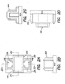
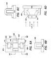
FIGS. 1A-D are block diagrams of respective top, first cross-sectional front, second cross-sectional front and cross-sectional side views of a substrate following a step of a method of manufacturing a finFET in which a body region having source/drain diffusion regions and a gate region are formed in accordance with an embodiment of the present invention. - F
IGS. 2A-D are block diagrams of respective top, first cross-sectional front, second cross-sectional front and cross-sectional side views of the substrate following a step of the method of manufacturing a finFET in which spacers are formed adjacent the body region and gate region in accordance with an embodiment of the present invention. -
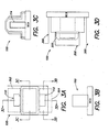
FIGS. 3A-D are block diagrams of respective top, first cross-sectional front, second cross-sectional front and cross-sectional side views of the substrate following a step of the method of manufacturing a finFET in which one or more portions of the spacers are removed from the substrate in accordance with an embodiment of the present invention. -
FIGS. 4A-D are block diagrams of respective top, first cross-sectional front, second cross-sectional front and cross-sectional side views of the substrate following a step of the method of manufacturing a finFET in which porous silicon is formed in the source/drain diffusion regions in accordance with an embodiment of the present invention. -
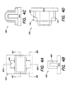
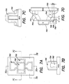
FIGS. 5A-D are block diagrams of respective top, first cross-sectional front, second cross-sectional front and cross-sectional side views of the substrate following a step of the method of manufacturing a finFET in which the substrate undergoes a second implant in accordance with an embodiment of the present invention. -
FIGS. 6A-D are block diagrams of respective top, first cross-sectional front, second cross-sectional front and cross-sectional side views of the substrate following a step of the method of manufacturing a finFET in which the substrate undergoes a third implant in accordance with an embodiment of the present invention. -
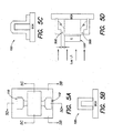
FIGS. 7A-D are block diagrams of respective top, first cross-sectional front, second cross-sectional front and cross-sectional side views of the substrate following a step of the method of manufacturing a finFET in which silicide is formed on the substrate in accordance with an embodiment of the present invention. -
FIGS. 8A-D are block diagrams of respective top, first cross-sectional front, second cross-sectional front and cross-sectional side views of the substrate following a step of the method of manufacturing a finFET in which back-end-of-line (BEOL) processing is performed in accordance with an embodiment of the present invention. -
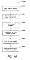
FIG. 9 illustrates a process flow of the method of manufacturing the finFET in accordance with an embodiment of the present invention. -
FIG. 10 illustrates sub-steps of a step in the process flow in which porous silicon is formed in source/drain diffusion regions in accordance with an embodiment of the present invention. - The present invention provides methods of manufacturing an improved fin MOSFET (FinFET). More specifically, the present invention provides a method of manufacturing a finFET with silicide formed on a top surface of and sidewalls of silicon in at least one source/drain diffusion region of the finFET. In this manner, the source/drain diffusion region includes an interior unsilicided region (e.g., silicon) nearly surrounded by silicide. Therefore, an area of an interface of the silicide and silicon in the finFET source/drain diffusion region is increased compared to conventional finFETs. Consequently, a resistance of the finFET manufactured in accordance with an embodiment of the present invention may be reduced compared to conventional finFETs.
- To form the silicide around portions of silicon in the source/drain diffusion region as described above, portions of silicon in the source/drain diffusion region are converted to porous silicon. Thereafter, a layer of metal may be deposited on the substrate. Silicidation is be employed to cause the metal to react with silicon of the substrate such that silicide is formed around portions of silicon in the source/drain diffusion region as described above. In this manner, the present invention provides methods of manufacturing an improved finFET.
-
FIGS. 1A-D are block diagrams of respective top, first cross-sectional front, second cross-sectional front and cross-sectional side views of a substrate following a step of a method of manufacturing a finFET in which a body region having source/drain diffusion regions and a gate region are formed in accordance with an embodiment of the present invention. With reference toFIGS. 1A-D , asubstrate 100 is provided. Thesubstrate 100 may include a silicon-on-insulator (SOI) layer. Alternatively, thesubstrate 100 may include a bulk substrate layer. Although a method of manufacturing a finFET with a reduced source-drain resistance is described below with reference to an SOI substrate, the present invention includes methods of manufacturing a finFET with a reduced source-drain resistance on a bulk substrate. Such methods may employ different isolation techniques. - The
substrate 100 may include a layer of silicon 102 (e.g., single crystal silicon) formed on a layer of oxide (e.g., buried oxide) 104. RIE or another suitable method may be employed to remove portions of thesilicon layer 102 such that abody region 106 may be formed. Thebody region 106 may include at least one source/drain diffusion region and define agate channel region 108. Further, thebody region 106 may include one or more source/drain contact regions 107. For example, thebody region 106 may include a first source/drain diffusion region 110 and a second source/drain diffusion region 112. Chemical vapor deposition (CVD) or another suitable method may be employed to form a layer ofdielectric material 114 and/or another suitable material around thebody region 106. As shown, thebody region 106 may be a "dog bone"-shaped silicon island (although the body region may have a different shape). In this manner, thebody region 106 may provide an increased contact area and/or an area within the source/drain diffusion region portion 115 of thebody region 106 between the first and second source/drain diffusion regions 110-112 may serve as a silicon fin of the finFET being manufactured. The fin may have a height h of about 50 nm to about 500 nm and a width w1 of about 5 nm to about 100 nm (although a larger or smaller and/or different height range may be employed). In this manner, the fin may be design to be narrow enough to enable fully-depleted body operation which may result in volume inversion, high carrier mobility and/or increased control of electric potential in thebody region 106. Consequently, the finFET being manufactured may provide an "on"/"off" current ratio that is superior to a planar MOSFET. - CVD or another suitable method may be employed to deposit a layer of
polysilicon material 116 or another suitable material on thesubstrate 100, and a layer ofnitride 118 or another suitable material thereon. RIE or another suitable method may be employed to remove portions of thepolysilicon material layer 116 andnitride layer 118 such that thepolysilicon material layer 116 andnitride layer 118 are formed on a portion of thebody region 106 between source/drain diffusion regions polysilicon material layer 116 anddielectric layer 114 may serve as a gate 120 (e.g., gate region or stack) of finFET being manufactured. More specifically, thepolysilicon material layer 116 may serve as a gate conductor layer. Further, thenitride layer 118 may serve as a gate capping layer. Consequently, thegate 120 may be formed around multiple (e.g., three) sides of thebody region 106. For example, a three-sided gate 120 may be formed on portions of opposing approximately vertical sidewalls and a portion of a top surface of thebody region 106. Thegate 120 may have alength 1 of about 18 nm to about 130 nm (although a larger or smaller and/or different length range may be employed). Thelength 1 of thegate 120 may determine the length of a channel formed in the finFET. -
FIGS. 1A-8D are not drawn to scale. For example, for illustrative purposes a width w1 of the fin and a width w2 of the gate conductor layer are intentionally enlarged. However, in an actual finFET device both the width w1, w2 of the gate conductor and the fin are significantly narrower than that shown in these drawings. -
FIGS. 2A-D are block diagrams of respective top, first cross-sectional front, second cross-sectional front and cross-sectional side views of the substrate following a step of the method of manufacturing a finFET in which spacers are formed adjacent the body region and gate region in accordance with an embodiment of the present invention. With reference toFIGS. 2A-D , CVD or another suitable method may be employed to form a layer of silicon nitride or another suitable material on thesubstrate 100. RIE or another suitable method may be employed to remove portions of the silicon nitride layer such thatspacers 200 are formed adjacent sidewalls of thebody region 106 and thegate 120. Thespacers 200 may be about 10 nm to about 100 nm wide (although a larger or smaller and/or different width range may be employed). During RIE to form thespacers 200, portions of thedielectric material layer 114 may be removed. For example, portions of thedielectric material layer 114 on a top surface of source/drain diffusion regions body region 106 may be removed. - The
spacers 200 may serve as sacrificial or temporary spacers employed to protect portions of thegate conductor layer 116 during subsequent processing. In this manner, a spacer width may be employed such that subsequently-formed silicide may be prevented from penetrating into a junction of the finFET as described below. Penetration of the silicide into the junction regions of the source/drain diffusion regions may result in severe leakage currents and must be avoided. -
FIGS. 3A-D are block diagrams of respective top, first cross-sectional front, second cross-sectional front and cross-sectional side views of the substrate following a step of the method of manufacturing a finFET in which one or more portions of the spacers are removed from the substrate in accordance with an embodiment of the present invention. With reference toFIGS. 3A-D , a spin-on technique or another suitable method may be employed to deposit a photoresist layer or another suitable material layer on thesubstrate 100. The photoresist layer may be patterned with a mask such that portions of the photoresist layer may be removed during a subsequent process (e.g., developing). In this manner atrim mask 300 may be formed. Although thetrim mask 300 described above comprises photoresist, in some embodiments, the trim mask may comprise a hard mask material.Dotted boxes substrate 100 that may be exposed by thetrim mask 300 during subsequent processing. For example, thetrim mask 300 may be employed duringRIE or another suitable method to remove portions of thespacers 200 and/or thedielectric material layer 114 adjacent source/drain diffusion regions body region 106. In this manner, a larger area of the source/ drain diffusion regions 110-112 (e.g., including sidewalls thereof) may be exposed during subsequent processing, thereby improving contact to the source/drain diffusion regions thereof. -
FIGS. 4A-D are block diagrams of respective top, first cross-sectional front, second cross-sectional front and cross-sectional side views of the substrate following a step of the method of manufacturing a finFET in whichporous silicon 400 is formed in the source/drain diffusion regions FIGS. 4A-D , impurity atoms (e.g., dopant) may be introduced into exposed portions of thesubstrate 100. For example, exposed portions of thesubstrate 100, such as source/drain diffusion regions substrate 100. - An anodization process may be employed to convert the doped (e.g., p+ doped) silicon to porous silicon. For example, contactless anodization such as that described in "A technique to form a porous silicon layer with no backside contact by alternating current electrochemical process," A. El-Bahar, Y. Nemirovsky, Applied Physics Letters, v 77, n 2, may be employed to form porous silicon in an SOI layer, which is electrically insulated from a contacted substrate. During such anodization, an AC voltage excitation may be applied to the
substrate 100, with theinsulated silicon layer 102 being capacitively coupled to thesubstrate 100. A reaction that forms theporous silicon 400 in the source/drain diffusion regions 110-112 may occur while an AC anode, which may be positive relative to the cathode, is excited. A fluoride-containing acidic electrolyte solution or the like may be employed for etching (e.g., anodic etching) during anodization. In this manner, a contactless anodization method (e.g., a method which may not require direct electrical contact with the substrate 100) may be employed to formporous silicon 400 as described above. In some embodiments, an excitation frequency of between about 500 Hz and about 10 kHz, an RMS current density of about_5 mA/cm2 to about 200mA/cm2, and silicon regions having a p+ doping concentration of greater than about 1019/cm3 may be may be employed to form the porous silicon 400 (although a larger or smaller and/or different range may be employed for the excitation frequency, current density and/or doping concentration). In this manner, pores (e.g., canals) having a diameter of about 1 nm to about 100 nm may be formed. A density of such pores ranges from about 109 pores/cm2 to about 1015 pores/cm2. However, a larger or smaller and/or different diameter and/or density range may be employed. Consequently, pores of theporous silicon 400 may occupy about 30% to about 80% of an overall volume of the silicon 400 (although the pores may occupy a larger or smaller and/or different percentage range of the overall volume). - A stripper bath or another suitable method may be employed to remove the
trim mask 300 from thesubstrate 100. Further, thesubstrate 100 may undergo annealing to remove excess dopant from theporous silicon 400. For example, thesubstrate 100 may undergo a hydrogen-ambient bake after theporous silicon 400 is formed such that some or all of the p+ dopant remaining in the source/drain diffusion regions 110-112 may be removed. During the hydrogen-ambient bake, thesubstrate 100 may be subjected to a temperature of about 850 °C to about 1100 °C for about 10 seconds to about 30 minutes (although a larger or smaller and/or different temperature range and/or time period may be employed). -
FIGS. 5A-D are block diagrams of respective top, first cross-sectional front, second cross-sectional front and cross-sectional side views of the substrate following a step of the method of manufacturing a finFET in which the substrate undergoes a second implant in accordance with an embodiment of the present invention. With reference toFIGS. 5A-D , RIE or another suitable method may be employed to remove portions (e.g., remaining portions) of thespacers 200. Additionally, isotropic etching or another suitable method may be employed to remove exposed portions of thenitride layer 118 and/or thedielectric layer 114 from thesubstrate 100. In this manner, portions of thespacers 200 and/or thenitride layer 118 remaining while theporous silicon 400 is formed served to protect the gate 120 (e.g., polysilicon material layer 116'and dielectric layer 114) while forming theporous silicon 400. Further, thespacers 200 served to position an edge (e.g., sidewall) of the porous silicon 400 a predetermined distance d (e.g., based on the width of the spacers 200) from thegate 120. In this manner, a leakage current between such regions may be reduced and/or prevented. For example, a spiking through of a source/drain metal into a gate channel of the finFET may be reduced and/or eliminated. Consequently, the width of thespacer 200 may be employed such that subsequently-formed silicide may be prevented from penetrating into a gate-source/drain junction. - The
substrate 100 may be subjected to angled ion implantations (Ldd I/I), such that lightly-doped source/drain diffusion (LDD) regions are formed within the N-channel and P-channel finFETs. For example, in accordance with standard MOSFET technology, a concentration of about 1 x 1018 cm-3 to about 5 x 1019 cm-3 may be employed for the LDD regions (although a larger or smaller and/or different concentration range may be employed). Standardly practiced LDD dopants such as arsenic, phosphorus or antimony N-type dopant species may be used for the N-channel finFETs, and boron or indium P-type species for the P-channel finFETs. In this manner, thesubstrate 100 may be lightly doped. More specifically, aregion 500 of relatively low doping close to thegate 120 may be formed in the source/drain diffusion regions -
FIGS. 6A-D are block diagrams of respective top, first cross-sectional front, second cross-sectional front and cross-sectional side views of the substrate following a step of the method of manufacturing a finFET in which the substrate undergoes a third implant in accordance with an embodiment of the present invention. With reference toFIGS. 6A-D , CVD or another suitable method followed by RIE or another suitable method may be employed to form spacers 600 (e.g., permanent spacers) on sidewalls of thegate 120 and sidewalls of thebody region 106 including the source/drain diffusion regions spacers 600 may be less than the previously-formedspacers 200. For example, thespacers 600 may be about 5 nm to about 50 nm wide (although a larger or smaller and/or different width range may be employed). - The
substrate 100 may be subjected to implantation, such as a source/drain ion implant (S/D I/I) or the like, such that junctions (e.g., of the source/drain diffusion regions 110, 112) of the finFET being manufactured may be formed. For example, a concentration of about 1 x 109 cm-3 to about 5x1020 cm-3 of dopant may be introduced into the substrate 100 (although a larger or smaller and/or different concentration range and/or dopant type may be employed). In this, manner, thesubstrate 100 may be heavily doped with impurity atoms. For example, an angled source-drain ion implant S/D I/I may be performed through theporous silicon 400 to form a doped (e.g., heavily doped silicon) region underneath theporous silicon 400. Further, a gate conductor work function of the finFET being manufactured may be based on such doping. In this manner, agate 120 has a work function which generally matches (e.g., is approximately equal to) the work function of the adjacent source-drain diffusions. - The second implant (e.g., light doping of the source/
drain diffusion regions 110, 112) and the third implant (e.g., heavy doping of the source/drain diffusion regions 110, 112) are performed afterporous silicon 400 is formed in the source/drain diffusion regions substrate 100 during the second and third implants may penetrate through theporous layer 400 and form a junction. It should be noted thespacers 200 may cause theporous silicon 400 to be formed a predetermined distance (e.g., based on a width of the spacer 200) from a source-drain junction near thegate 120. Such distance may prevent silicide subsequently formed in theporous silicon 400 from encroaching (e.g., laterally) on such junction. - Implantation of impurity atoms through the
porous silicon 400 during the third implant enables formation of heavy source-drain doping much deeper than theporous silicon 400 after thesubstrate 100 undergoes annealing. As described below, theporous silicon 400 is converted to a highly-conductive metallic silicide. Such silicide should not encroach (e.g., penetrate or spike through) the junctions. To reduce and/or eliminate such penetration (e.g., lateral penetration),spacer 200 is wider than thespacer 600, which may be employed to separate the lightly-doped and heavily-doped implants of the source/drain diffusion regions porous silicon 400 upon the source/drain diffusion regions gate 120 so that a series resistance can be significantly reduced. However, closer to the gate 120 (e.g., along the edges of thepolysilicon material layer 116 serving as the gate conductor) only a very shallow surface layer of the source/drain diffusion regions - Thereafter, the
substrate 100 may undergo annealing or another suitable process. For example, following the light and heavy doping of the source/drain diffusion regions 110, 112 (among other regions), thesubstrate 100 may be subjected to a dopant activation anneal, such as a rapid thermal anneal (RTA) or spike anneal at a temperature between about 950 °C and about 1150 °C for about 5 seconds to about 30 seconds (although a larger or smaller and/or different temperature and/or time period range may be employed). Further, a different type of annealing may be employed. -
FIGS. 7A-D are block diagrams of respective top, first cross-sectional front, second cross-sectional front and cross-sectional side views of the substrate following a step of the method of manufacturing a finFET in which silicide is formed on the substrate in accordance with an embodiment of the present invention. With reference toFIGS. 7A-D , CVD or another suitable method may be employed to form a layer of metal, such as tungsten, cobalt, titanium, nickel and/or the like, on thesubstrate 100. - Thereafter, the
substrate 100 undergoes silicidation. Silicidation of different regions of thesubstrate 100 may lower series resistance and enable better current drivability of the finFET. During silicidation, the metal may react with different portions of silicon on thesubstrate 100 such that silicide forms therein. For example, theporous silicon 400 is silicided. More specifically, metal may be soaked into pores of theporous silicon 400. Silicidation may proceed more rapidly through theporous silicon 400 than through remaining portions of silicon in the source/drain diffusion regions substrate 100. Consequently, a time period for silicidation of theporous silicon 400 and/or remaining portions of the finFET may be reduced.
Further, a depth of asilicide layer 700 formed on thesubstrate 100 may be precisely controlled. More specifically, silicon in the entire source/drain diffusion regions drain diffusion regions interface 704 of thesilicide layer 700 andunsilicided silicon region 702 is increased compared to a transistor having silicide formed only on a top surface of source/drain diffusion regions of the transistor and compared to a transistor having silicide formed in the entire source/drain diffusion region of the transistor. A resistance (e.g., a source-drain resistance) of a finFET may be based on (e.g., inversely proportional to) the area of such interface. Consequently, the unsilicided silicon "core" 702 formed by the present invention may reduce a series resistance of the finFET being manufactured. Further, the finFET may employ the unsilicided silicon "core" 702 to avoid reducing an area normal to the direction of the current density crossing the silicide/unsilicided silicon interface in source/drain diffusion regions - Process parameters employed while forming the
porous silicon 400 may determine thicknesses of respective portions of theporous silicon 400. A thickness of the subsequently-formed silicide may be based on the porous silicon layer thickness. Therefore, the present invention may be employed to form a silicide layer 700 (as described above) portions of which may be thinner than a conventional silicide layer. In this manner, the present invention may be employed in finFETs with shallow junctions. - The
silicide layer 700 formed in a source/drain diffusion region first portion 706 having a thickness t1 of about 1 nm to about 5 nm (although a larger or smaller and/or different thickness range may be employed).Such portion 706 may serve as a contact (e.g., a thin contact) to the LDD silicon. Additionally, thesilicide layer 700 formed in the source/drain diffusion region second portion 708 having a thickness t2 of about 5 nm to about 100 nm (although a larger or smaller and/or different thickness range may be employed).Such portion 708 may serve as a contact (e.g., a thicker contact) to a top surface of silicon in the source/drain diffusion region silicide layer 700 formed in the source/drain diffusion region third portion 710 having a width w1 of about 5 nm to about 100 nm (although a larger or smaller and/or different width range may be employed).Such portion 710 may serve as a contact to sidewalls of silicon in the source/drain diffusion region silicide layer 700 may form or define a region of silicon in the interior of the source/drain diffusion region 110, 112 (e.g., the unsilicided silicon "core" 702). Although a specific shape is described above for thesilicide layer 700 in the source/drain diffusion regions silicide layer 700 in the source/drain diffusion regions interface 704 of thesilicide layer 700 and silicon in the source/drain diffusion region - Thereafter, RIE or another suitable method may be employed to remove unreacted metal from the
substrate 100. Such RIE may be selective to silicide. -
FIGS. 8A-D are block diagrams of respective top, first cross-sectional front, second cross-sectional front and cross-sectional side views of the substrate following a step of the method of manufacturing a finFET in which back-end-of-line (BEOL) processing is performed in accordance with an embodiment of the present invention. With reference toFIGS. 8A-D , CVD or another suitable method may be employed to deposit aninsulator layer 800, such as a planarizing glass (e.g., undoped TEOS, phosphosilicate glass (PSG), borosilicate glass (BSG), borophosphosilicate glass (BPSG) and/or the like) on a top surface of thesubstrate 100. Thereafter, theinsulator layer 800 may be planarized. In some embodiments, the insulator may be reflowed to planarize theinsulator layer 800. Alternatively, chemical mechanical polishing (CMP) or another suitable method may be employed to planarize theinsulator layer 800. RIE or another suitable method may be employed to form one or more vias orcontact openings 802 on thesubstrate 100. CVD or another suitable method followed by RIE, CMP or another suitable method may be employed to fillsuch vias 802 with a conductor, such as tungsten or another suitable material, thereby formingstuds 804. Additionally, one or more levels of wiring and/or interlevel dielectric may be formed on thesubstrate 100. In this manner, animproved finFET 806 may be formed. ThefinFET 806 has a reduced source-drain resistance compared to conventional transistors. ThefinFET 806 includes at least one source/drain diffusion region drain diffusion regions drain diffusion region finFET 806 may include asilicide layer 700 having a thin silicide region (e.g., the first portion 706) located in the vicinity of agate channel region 808 of thefinFET 806, a thicker silicide region (e.g., the second portion 708) located in a distance away from thegate channel region 808, sidewall silicide regions (e.g., the third portion 710) which may be coupled to and/or included in outer edges of the source/drain diffusion region unsilicided silicon region 702 in the interior of the source/drain diffusion region -
FIG. 9 illustrates aprocess flow 900 of the method of manufacturing the finFET in accordance with an embodiment of the present invention. With reference toFIG. 9 , during the method of manufacturing thefinFET 806, instep 902, thegate region 120 may be protected (e.g., by the trim mask 300) and the source/drain diffusion regions porous silicon 400 is formed in portions of the source/drain diffusion regions conductor material layer 116, and thegate dielectric 114 is protected from damage due to the etching action of the electrolyte used to form pores in the exposed silicon. Consequently, subsequent doping and/or silicidation of thegate region 120 may be controlled. Therefore, thegate region 120 may not be doped more than desired, thereby avoiding a problem of removing a dopant, such as boron, from grain boundaries of the gate conductor material. Further, a larger portion (depth) than that desired of thegate region 120 may not be silicided, which would adversely affect a work function at an edge of the gate region 120 (e.g., for a short channel device) and threshold voltage of thefinFET 806. - In
step 904, porosity (e.g., porous silicon 400) is formed in selected areas of the source/drain diffusion regions step 904 are described below with reference toFIG. 10 . After theporous silicon 400 is formed, implant and annealing process steps may be employed to form the source/drain diffusion regions finFET 806. For example, instep 906, dopant may be implanted into thesubstrate 100. For example, the LDD I/I and the S/D I/I may be employed to dope thegate region 120 and form junctions in the source/drain diffusion regions step 908, silicidation is employed to form thesilicide layer 700 on the substrate 100 (e.g., on thegate region 120 and on theporous silicon 400 of the source/drain diffusion regions 110, 112). Thesilicide layer 700 is formed inside theporous silicon 400 and may as well be formed at exposed surfaces of single-crystal silicon and polysilicon on thesubstrate 100. Thereafter, step 910 may be performed. Instep 910, BEOL processing may continue. For example, theinsulator layer 800, vias orcontact openings 802,studs 804, interlevel dielectrics, wiring levels and/or the like may be formed such that contact may be made to thefinFET 806. In this manner, the low source-drain resistance finFET 806 may be formed. -
FIG. 10 illustrates sub-steps 1000 of a step in theprocess flow 900 in which porous silicon is formed in source/drain diffusion regions in accordance with an embodiment of the present invention. With reference toFIG. 10 , to performstep 904, instep 1002, dummy spacers such as the sacrificial ortemporary spacers 200 may be formed on thesubstrate 100. Thetemporary spacers 200 may be formed adjacent thegate region 120 andbody region 106 of thesubstrate 100. Instep 1004, portions of thetemporary spacers 200 adjacent source/drain diffusion regions body region 106 may be removed using isotropic etching or the like. Such portions may be exposed during etching by thetrim mask 300. Trimming away portions of thespacers 200 around the outer edges of the source/drain diffusion regions porous silicon 400. Instep 1006, dopant (e.g., p+ dopant such as boron and/or the like) may be introduced into exposed portions of thesubstrate 100. Plasma immersion implantation, ion implantation (e.g., angled), gas phase doping, a solid source doping technique or conventional gaseous source diffusion process may be employed to dope the exposed portions of thesubstrate 100. In this manner, the source/drain diffusion regions porous silicon 400 is formed. - Thereafter, in
step 1008, thesubstrate 100 may undergo anodization such that pores form inside the p+ doped regions of the source/drain diffusion regions step 1010, remaining portions of thetemporary spacers 200 may be stripped from thesubstrate 100. RIE or another suitable method may be employed. Further, instep 1012, thesubstrate 100 may undergo annealing to remove excessive dopant therefrom. For example, thesubstrate 100 may be subjected to a hydrogen bake (e.g., a low temperature bake in a hydrogen ambient) such that excess p+ dopant inserted in thesubstrate 100 duringstep 1006 may be removed (e.g., depleted by the bake). Through use of the present method, afinFET 806 with a unique and robust source-drain contacting scheme may be formed. - Conventional methods and apparatus for semiconductor device manufacturing pose problems. For example, when scaling CMOS technology below the 45nm node, processes associated with the formation of a gate electrode, including the gate stack and dielectric, the channel and the source/drain regions all have to be significantly modified from earlier technology generations. Effective mitigation of short channel effects requires ever shallower junction depths. Additionally, SOI film thickness and finFET fin width also must be reduced for short channel scalability. Unless raised source/drain structures are implemented, a thinner silicide is required to cope with the shallower junctions and thinner materials. Silicidation of'source-drain diffusions is required to lower series resistance for better current drivability. However, consumption of silicon under silicide leads to increased contact resistance due to dopant depletion effects. Increased source-drain doping concentration may be employed to attempt to resolve this problem. However, high doping concentration may not easily be obtained due to limitations of solid solubility and electrical activation. Furthermore, a significant fraction of the source-drain series resistance is due to the interface between the silicide layer and the silicon. This leads to sharply increased series resistance when silicide is formed completely through the source-drain silicon because a channel current is forced to flow through a small cross-sectional area dictated by the thickness of the SOI film or by the width of the FinFET fin.
- Therefore, a portion of the silicon normal to the surface of the source-drain diffusion should remain unsilicided. However, it is a great challenge to reduce contact resistance between a thin silicide layer and shallow source/drain. The problem is further complicated when contacting the source-drain diffusions of conventional finFETs because sidewalls of the source-drain regions of such finFETs are covered by the spacers as a consequence of the gate'processing. Therefore, silicidation of such finFET source-drain diffusions is limited to the horizontally oriented surfaces, and not the sidewalls. This results in greatly compromised source-drain resistance and degraded performance of the conventional device.
- The present methods may provide advantages over conventional finFETs and avoid the disadvantages of conventional finFETs described above. For example, by forming the
sacrificial spacer 200 before forming theporous silicon 400, the subsequently-formedsilicide layer 700 may be prevented from encroaching on metallurgical junctions. In this manner, thefinFET 806 may avoid the high leakage currents of conventional finFETs by maintaining a low-junction leakage current. Further, a gate electrode of thefinFET 806 may be protected while formingporous silicon 400 in the source/drain diffusion region finFET gate 120 has a preferred work-function. - In a conventional finFET, a source and drain region may contribute a high series resistance to the finFET. As the aspect ratio (fin height/width) of the body of such conventional finFET increases, a contact resistance problem increases. More specifically, because the sidewalls of the source/drain diffusion regions of such finFETs are often blocked by spacer material associated with gate formation, doping and silicidation occurs only on portions of a top surface of the source/drain diffusion regions. Further, a contact region on a top surface of the source/drain diffusion area is narrow, resulting in high contact resistance.
- In contrast, by converting at least a portion of silicon in the source/
drain diffusion regions porous silicon 400, subsequently-formed silicide of the present invention may have a larger contact surface area than the planar surface area of the source/drain diffusion region silicide layer 700 may form on four sides (e.g., on three sidewalls and a top surface) of the source/drain diffusion region finFET 806. For the above reasons, compared to conventional transistors, thefinFET 806 has a reduced source-drain series resistance. - Further, a source/drain ion implant is performed on the
substrate 100 after forming theporous silicon 400 so that after drive-in of dopant a junction is always formed beneath the layer ofporous silicon 400. Thereafter, the entire region ofporous silicon 400 may be converted to silicide. Because the silicide forms mainly inside the region ofporous silicon 400, dopant depletion problems are reduced and/or eliminated. - The foregoing description discloses only exemplary embodiments of the invention. Modifications of the above disclosed apparatus and methods which fall within the scope of the claims will be readily apparent to those of ordinary skill in the art. For instance, although the second implant described above is an LDD I/I, alternatively or additionally, the
substrate 100 may be subjected to a halo implants or the like. For example, a concentration of about 5 x 1017 cm-3 to about 5x1018 cm-3 may be employed of dopant polarity opposite of the source-drain doping polarity may be implanted into the substrate 100 (although a larger or smaller and/or different concentration range and/or dopant type may be employed). The halo implant may be employed to adjust a threshold voltage of thefinFET 806 being manufactured.
Claims (6)
- A method of manufacturing a finFET, comprising:providing a substrate (100); andforming at least one source/drain diffusion region (110, 112) of the finFET on the substrate (100);wherein each source/drain diffusion region includes:an interior region of unsilicided silicon (702); andsilicide (700) formed on a top surface and sidewalls of the region of unsilicided silicon (702); characterised in that the step of forming at least one source/drain diffusion region (110, 112) further comprises the steps offorming a region of silicon (106) on the substrate (100);converting one or more portions of the silicon (106) in the region to porous silicon (400), and silicidation of the porous silicon (400) to form the silicide (700) on a top surface and sidewalls of the region of unsilicided silicon (702).
- The method of claim 1 wherein converting one or more portions of the silicon (106) in the region to porous silicon (400) includes employing a contactless anodization process to convert one or more portions of the silicon (106) in the region to porous silicon (400).
- The method of claim 2 wherein converting one or more portions of the silicon (106) in the region to porous silicon (400) further includes removing portions of a previously-implanted dopant from the substrate (100) using annealing.
- The method of claim 2 further comprising employing a spacer (200) to separate the porous silicon (400) from a gate region (120) of the finFET by a predetermined distance.
- The method of claim 1 wherein forming at least one source/drain diffusion region (110, 112) on the substrate (100) further includes:depositing a layer of metal on the substrate (100); andcausing the metal to react with at least the porous silicon (400) such that silicide is formed on a top surface and sidewalls of the region of silicon (106).
- The method of claim 1 further comprising forming a gate (120) having a predetermined work function on the substrate (100).
Applications Claiming Priority (2)
| Application Number | Priority Date | Filing Date | Title |
|---|---|---|---|
| US11/316,244 US7531423B2 (en) | 2005-12-22 | 2005-12-22 | Reduced-resistance finFETs by sidewall silicidation and methods of manufacturing the same |
| PCT/EP2006/069339 WO2007071555A1 (en) | 2005-12-22 | 2006-12-05 | Reduced-resistance finfets and methods of manufacturing the same |
Publications (2)
| Publication Number | Publication Date |
|---|---|
| EP1964179A1 EP1964179A1 (en) | 2008-09-03 |
| EP1964179B1 true EP1964179B1 (en) | 2009-09-02 |
Family
ID=37771049
Family Applications (1)
| Application Number | Title | Priority Date | Filing Date |
|---|---|---|---|
| EP06830385A Active EP1964179B1 (en) | 2005-12-22 | 2006-12-05 | Methods of manufacturing reduced-resistance finfets |
Country Status (8)
| Country | Link |
|---|---|
| US (2) | US7531423B2 (en) |
| EP (1) | EP1964179B1 (en) |
| JP (1) | JP4550146B2 (en) |
| KR (1) | KR100992037B1 (en) |
| CN (1) | CN101317273B (en) |
| AT (1) | ATE441938T1 (en) |
| DE (1) | DE602006008984D1 (en) |
| WO (1) | WO2007071555A1 (en) |
Families Citing this family (40)
| Publication number | Priority date | Publication date | Assignee | Title |
|---|---|---|---|---|
| US7479437B2 (en) * | 2006-04-28 | 2009-01-20 | International Business Machines Corporation | Method to reduce contact resistance on thin silicon-on-insulator device |
| KR100864928B1 (en) * | 2006-12-29 | 2008-10-22 | 동부일렉트로닉스 주식회사 | Method of Forming ?????? Device |
| US20090001426A1 (en) * | 2007-06-29 | 2009-01-01 | Kangguo Cheng | Integrated Fin-Local Interconnect Structure |
| US8063437B2 (en) * | 2007-07-27 | 2011-11-22 | Panasonic Corporation | Semiconductor device and method for producing the same |
| US8004045B2 (en) | 2007-07-27 | 2011-08-23 | Panasonic Corporation | Semiconductor device and method for producing the same |
| US8021939B2 (en) * | 2007-12-12 | 2011-09-20 | International Business Machines Corporation | High-k dielectric and metal gate stack with minimal overlap with isolation region and related methods |
| EP2311072B1 (en) * | 2008-07-06 | 2013-09-04 | Imec | Method for doping semiconductor structures |
| US20110001169A1 (en) * | 2009-07-01 | 2011-01-06 | International Business Machines Corporation | Forming uniform silicide on 3d structures |
| US8653608B2 (en) * | 2009-10-27 | 2014-02-18 | Taiwan Semiconductor Manufacturing Company, Ltd. | FinFET design with reduced current crowding |
| US8278179B2 (en) | 2010-03-09 | 2012-10-02 | Taiwan Semiconductor Manufacturing Co., Ltd. | LDD epitaxy for FinFETs |
| US8431995B2 (en) * | 2010-05-13 | 2013-04-30 | International Business Machines Corporation | Methodology for fabricating isotropically recessed drain regions of CMOS transistors |
| US8716798B2 (en) | 2010-05-13 | 2014-05-06 | International Business Machines Corporation | Methodology for fabricating isotropically recessed source and drain regions of CMOS transistors |
| JP5837307B2 (en) * | 2011-02-07 | 2015-12-24 | 公益財団法人神奈川科学技術アカデミー | Method for producing porous fine particles |
| US8614134B2 (en) * | 2011-03-21 | 2013-12-24 | Globalfoundries Inc. | Shallow source and drain architecture in an active region of a semiconductor device having a pronounced surface topography by tilted implantation |
| US10629900B2 (en) | 2011-05-04 | 2020-04-21 | Corning Incorporated | Porous silicon compositions and devices and methods thereof |
| CN103137478A (en) * | 2011-11-21 | 2013-06-05 | 中芯国际集成电路制造(上海)有限公司 | Manufacturing method and structure of fin field-effect transistor (FinFET) device |
| US8637931B2 (en) | 2011-12-27 | 2014-01-28 | International Business Machines Corporation | finFET with merged fins and vertical silicide |
| KR101894221B1 (en) | 2012-03-21 | 2018-10-04 | 삼성전자주식회사 | Field effect transistor and semiconductor device including the same |
| US8664072B2 (en) | 2012-05-30 | 2014-03-04 | Globalfoundries Inc. | Source and drain architecture in an active region of a P-channel transistor by tilted implantation |
| WO2014009991A1 (en) * | 2012-07-09 | 2014-01-16 | 国立大学法人東北大学 | Mosfet having 3d-structure and manufacturing method for same |
| US8975125B2 (en) * | 2013-03-14 | 2015-03-10 | International Business Machines Corporation | Formation of bulk SiGe fin with dielectric isolation by anodization |
| US8859379B2 (en) | 2013-03-15 | 2014-10-14 | International Business Machines Corporation | Stress enhanced finFET devices |
| US8940602B2 (en) | 2013-04-11 | 2015-01-27 | International Business Machines Corporation | Self-aligned structure for bulk FinFET |
| KR102083493B1 (en) | 2013-08-02 | 2020-03-02 | 삼성전자 주식회사 | Manufacturing method of a semiconductor device |
| US9583590B2 (en) | 2013-09-27 | 2017-02-28 | Samsung Electronics Co., Ltd. | Integrated circuit devices including FinFETs and methods of forming the same |
| US9711645B2 (en) * | 2013-12-26 | 2017-07-18 | International Business Machines Corporation | Method and structure for multigate FinFET device epi-extension junction control by hydrogen treatment |
| US9391173B2 (en) * | 2014-04-22 | 2016-07-12 | International Business Machines Corporation | FinFET device with vertical silicide on recessed source/drain epitaxy regions |
| CN105702725B (en) * | 2014-11-27 | 2018-12-11 | 中国科学院微电子研究所 | Semiconductor devices and its manufacturing method |
| CN105702729B (en) * | 2014-11-27 | 2019-01-15 | 中国科学院微电子研究所 | Semiconductor devices and its manufacturing method |
| US9741811B2 (en) | 2014-12-15 | 2017-08-22 | Samsung Electronics Co., Ltd. | Integrated circuit devices including source/drain extension regions and methods of forming the same |
| US9666716B2 (en) | 2014-12-15 | 2017-05-30 | Sang U. Kim | FinFET transistor |
| CN105789301B (en) * | 2014-12-25 | 2018-09-11 | 中国科学院微电子研究所 | Fin formula field effect transistor, fin structure and its manufacturing method |
| US9837277B2 (en) | 2015-08-12 | 2017-12-05 | International Business Machines Corporation | Forming a contact for a tall fin transistor |
| US9397197B1 (en) | 2015-09-23 | 2016-07-19 | International Business Machines Corporation | Forming wrap-around silicide contact on finFET |
| US9484251B1 (en) * | 2015-10-30 | 2016-11-01 | Lam Research Corporation | Contact integration for reduced interface and series contact resistance |
| CN108290740B (en) | 2015-11-25 | 2022-03-04 | 康宁股份有限公司 | Porous silicon composition and device and method thereof |
| CN107452792A (en) * | 2016-06-01 | 2017-12-08 | 中芯国际集成电路制造(上海)有限公司 | Semiconductor device and its manufacture method |
| US9853127B1 (en) * | 2016-06-22 | 2017-12-26 | International Business Machines Corporation | Silicidation of bottom source/drain sheet using pinch-off sacrificial spacer process |
| CN108155236B (en) * | 2016-12-05 | 2020-08-07 | 上海新昇半导体科技有限公司 | Low contact resistivity FinFET with black phosphorus channel layer and preparation method thereof |
| US10707331B2 (en) * | 2017-04-28 | 2020-07-07 | Taiwan Semiconductor Manufacturing Company, Ltd. | FinFET device with a reduced width |
Family Cites Families (15)
| Publication number | Priority date | Publication date | Assignee | Title |
|---|---|---|---|---|
| US6297135B1 (en) | 1997-01-29 | 2001-10-02 | Ultratech Stepper, Inc. | Method for forming silicide regions on an integrated device |
| JP3209164B2 (en) * | 1997-10-07 | 2001-09-17 | 日本電気株式会社 | Method for manufacturing semiconductor device |
| US6133124A (en) * | 1999-02-05 | 2000-10-17 | Advanced Micro Devices, Inc. | Device improvement by source to drain resistance lowering through undersilicidation |
| US6255214B1 (en) * | 1999-02-24 | 2001-07-03 | Advanced Micro Devices, Inc. | Method of forming junction-leakage free metal silicide in a semiconductor wafer by amorphization of source and drain regions |
| CA2455565C (en) * | 2001-07-25 | 2007-11-06 | Philmac Pty Ltd | Coupling or transition fitting for the connection of metal or plastic pipes |
| US7358121B2 (en) * | 2002-08-23 | 2008-04-15 | Intel Corporation | Tri-gate devices and methods of fabrication |
| US6864519B2 (en) * | 2002-11-26 | 2005-03-08 | Taiwan Semiconductor Manufacturing Co., Ltd. | CMOS SRAM cell configured using multiple-gate transistors |
| US7105894B2 (en) * | 2003-02-27 | 2006-09-12 | Taiwan Semiconductor Manufacturing Co., Ltd. | Contacts to semiconductor fin devices |
| KR100559572B1 (en) * | 2003-09-01 | 2006-03-10 | 동부아남반도체 주식회사 | Method for fabricating semiconductor device having salicide |
| US20050090067A1 (en) * | 2003-10-27 | 2005-04-28 | Dharmesh Jawarani | Silicide formation for a semiconductor device |
| KR100526889B1 (en) * | 2004-02-10 | 2005-11-09 | 삼성전자주식회사 | Fin field effect transistor structure |
| KR20050108916A (en) * | 2004-05-14 | 2005-11-17 | 삼성전자주식회사 | Methods of forming a fin field effect transistor using damascene process |
| JP3964885B2 (en) * | 2004-05-19 | 2007-08-22 | 株式会社東芝 | Semiconductor device and manufacturing method thereof |
| US7015126B2 (en) * | 2004-06-03 | 2006-03-21 | Taiwan Semiconductor Manufacturing Co., Ltd. | Method of forming silicided gate structure |
| JP2006012898A (en) * | 2004-06-22 | 2006-01-12 | Toshiba Corp | Semiconductor device and its manufacturing method |
-
2005
- 2005-12-22 US US11/316,244 patent/US7531423B2/en active Active
-
2006
- 2006-12-05 EP EP06830385A patent/EP1964179B1/en active Active
- 2006-12-05 CN CN2006800440556A patent/CN101317273B/en active Active
- 2006-12-05 AT AT06830385T patent/ATE441938T1/en not_active IP Right Cessation
- 2006-12-05 JP JP2008546349A patent/JP4550146B2/en active Active
- 2006-12-05 DE DE602006008984T patent/DE602006008984D1/en active Active
- 2006-12-05 KR KR1020087014763A patent/KR100992037B1/en not_active IP Right Cessation
- 2006-12-05 WO PCT/EP2006/069339 patent/WO2007071555A1/en active Application Filing
-
2007
- 2007-10-31 US US11/933,392 patent/US20080054349A1/en not_active Abandoned
Also Published As
| Publication number | Publication date |
|---|---|
| US20080054349A1 (en) | 2008-03-06 |
| CN101317273A (en) | 2008-12-03 |
| US7531423B2 (en) | 2009-05-12 |
| US20070148836A1 (en) | 2007-06-28 |
| EP1964179A1 (en) | 2008-09-03 |
| KR20080086458A (en) | 2008-09-25 |
| WO2007071555A1 (en) | 2007-06-28 |
| CN101317273B (en) | 2012-08-22 |
| DE602006008984D1 (en) | 2009-10-15 |
| ATE441938T1 (en) | 2009-09-15 |
| KR100992037B1 (en) | 2010-11-05 |
| JP4550146B2 (en) | 2010-09-22 |
| JP2009521113A (en) | 2009-05-28 |
Similar Documents
| Publication | Publication Date | Title |
|---|---|---|
| EP1964179B1 (en) | Methods of manufacturing reduced-resistance finfets | |
| US10134892B2 (en) | High voltage device with low Rdson | |
| US9570545B2 (en) | High voltage trench transistor | |
| US8822291B2 (en) | High voltage device | |
| US20070032029A1 (en) | Lateral trench power MOSFET with reduced gate-to-drain capacitance | |
| US20080042205A1 (en) | Low-cost high-performance planar back-gate cmos | |
| US8159024B2 (en) | High voltage (>100V) lateral trench power MOSFET with low specific-on-resistance | |
| US10580888B1 (en) | Oxygen inserted Si-layers for reduced contact implant outdiffusion in vertical power devices | |
| US9768295B2 (en) | Semiconductor devices having super-junction trenches with conductive regions and method of making the same | |
| CN108428743B (en) | Metal/polysilicon gate trench power MOSFET and method of forming the same | |
| US20130026565A1 (en) | Low rdson resistance ldmos | |
| US20220037468A1 (en) | MOS Transistor with Folded Channel and Folded Drift Region | |
| US20080169505A1 (en) | Structure of Trench MOSFET and Method for Manufacturing the same | |
| US6849546B1 (en) | Method for improving interlevel dielectric gap filling over semiconductor structures having high aspect ratios | |
| US8912066B2 (en) | Lateral double-diffused high voltage device | |
| US6395606B1 (en) | MOSFET with metal in gate for reduced gate resistance | |
| US9530884B2 (en) | Method of manufacturing a semiconductor device and semiconductor device | |
| KR101801406B1 (en) | Semiconductor device and related fabrication methods | |
| US7119017B2 (en) | Method for improving interlevel dielectric gap filling over semiconductor structures having high aspect ratios | |
| US20130049122A1 (en) | Semiconductor device and method of manufacturing the same | |
| US10749028B2 (en) | Transistor with gate/field plate structure | |
| Zhang et al. | High voltage device with low R dson |
Legal Events
| Date | Code | Title | Description |
|---|---|---|---|
| PUAI | Public reference made under article 153(3) epc to a published international application that has entered the european phase |
Free format text: ORIGINAL CODE: 0009012 |
|
| 17P | Request for examination filed |
Effective date: 20080619 |
|
| AK | Designated contracting states |
Kind code of ref document: A1 Designated state(s): AT BE BG CH CY CZ DE DK EE ES FI FR GB GR HU IE IS IT LI LT LU LV MC NL PL PT RO SE SI SK TR |
|
| RIC1 | Information provided on ipc code assigned before grant |
Ipc: H01L 21/8234 20060101ALI20090327BHEP Ipc: H01L 21/285 20060101ALI20090327BHEP Ipc: H01L 29/45 20060101ALI20090327BHEP Ipc: H01L 29/78 20060101ALI20090327BHEP Ipc: H01L 21/336 20060101AFI20090327BHEP |
|
| RTI1 | Title (correction) |
Free format text: METHODS OF MANUFACTURING REDUCED-RESISTANCE FINFETS |
|
| GRAP | Despatch of communication of intention to grant a patent |
Free format text: ORIGINAL CODE: EPIDOSNIGR1 |
|
| GRAS | Grant fee paid |
Free format text: ORIGINAL CODE: EPIDOSNIGR3 |
|
| GRAA | (expected) grant |
Free format text: ORIGINAL CODE: 0009210 |
|
| AK | Designated contracting states |
Kind code of ref document: B1 Designated state(s): AT BE BG CH CY CZ DE DK EE ES FI FR GB GR HU IE IS IT LI LT LU LV MC NL PL PT RO SE SI SK TR |
|
| REG | Reference to a national code |
Ref country code: CH Ref legal event code: NV Representative=s name: IBM RESEARCH GMBH ZURICH RESEARCH LABORATORY INTEL Ref country code: CH Ref legal event code: EP |
|
| REG | Reference to a national code |
Ref country code: IE Ref legal event code: FG4D |
|
| REF | Corresponds to: |
Ref document number: 602006008984 Country of ref document: DE Date of ref document: 20091015 Kind code of ref document: P |
|
| REG | Reference to a national code |
Ref country code: GB Ref legal event code: 746 Effective date: 20091027 |
|
| PG25 | Lapsed in a contracting state [announced via postgrant information from national office to epo] |
Ref country code: SE Free format text: LAPSE BECAUSE OF FAILURE TO SUBMIT A TRANSLATION OF THE DESCRIPTION OR TO PAY THE FEE WITHIN THE PRESCRIBED TIME-LIMIT Effective date: 20090902 Ref country code: LT Free format text: LAPSE BECAUSE OF FAILURE TO SUBMIT A TRANSLATION OF THE DESCRIPTION OR TO PAY THE FEE WITHIN THE PRESCRIBED TIME-LIMIT Effective date: 20090902 Ref country code: FI Free format text: LAPSE BECAUSE OF FAILURE TO SUBMIT A TRANSLATION OF THE DESCRIPTION OR TO PAY THE FEE WITHIN THE PRESCRIBED TIME-LIMIT Effective date: 20090902 |
|
| NLV1 | Nl: lapsed or annulled due to failure to fulfill the requirements of art. 29p and 29m of the patents act | ||
| LTIE | Lt: invalidation of european patent or patent extension |
Effective date: 20090902 |
|
| PG25 | Lapsed in a contracting state [announced via postgrant information from national office to epo] |
Ref country code: LV Free format text: LAPSE BECAUSE OF FAILURE TO SUBMIT A TRANSLATION OF THE DESCRIPTION OR TO PAY THE FEE WITHIN THE PRESCRIBED TIME-LIMIT Effective date: 20090902 Ref country code: NL Free format text: LAPSE BECAUSE OF FAILURE TO SUBMIT A TRANSLATION OF THE DESCRIPTION OR TO PAY THE FEE WITHIN THE PRESCRIBED TIME-LIMIT Effective date: 20090902 Ref country code: PL Free format text: LAPSE BECAUSE OF FAILURE TO SUBMIT A TRANSLATION OF THE DESCRIPTION OR TO PAY THE FEE WITHIN THE PRESCRIBED TIME-LIMIT Effective date: 20090902 Ref country code: SI Free format text: LAPSE BECAUSE OF FAILURE TO SUBMIT A TRANSLATION OF THE DESCRIPTION OR TO PAY THE FEE WITHIN THE PRESCRIBED TIME-LIMIT Effective date: 20090902 |
|
| PG25 | Lapsed in a contracting state [announced via postgrant information from national office to epo] |
Ref country code: CY Free format text: LAPSE BECAUSE OF FAILURE TO SUBMIT A TRANSLATION OF THE DESCRIPTION OR TO PAY THE FEE WITHIN THE PRESCRIBED TIME-LIMIT Effective date: 20090902 |
|
| PG25 | Lapsed in a contracting state [announced via postgrant information from national office to epo] |
Ref country code: RO Free format text: LAPSE BECAUSE OF FAILURE TO SUBMIT A TRANSLATION OF THE DESCRIPTION OR TO PAY THE FEE WITHIN THE PRESCRIBED TIME-LIMIT Effective date: 20090902 Ref country code: PT Free format text: LAPSE BECAUSE OF FAILURE TO SUBMIT A TRANSLATION OF THE DESCRIPTION OR TO PAY THE FEE WITHIN THE PRESCRIBED TIME-LIMIT Effective date: 20100104 Ref country code: IS Free format text: LAPSE BECAUSE OF FAILURE TO SUBMIT A TRANSLATION OF THE DESCRIPTION OR TO PAY THE FEE WITHIN THE PRESCRIBED TIME-LIMIT Effective date: 20100102 Ref country code: ES Free format text: LAPSE BECAUSE OF FAILURE TO SUBMIT A TRANSLATION OF THE DESCRIPTION OR TO PAY THE FEE WITHIN THE PRESCRIBED TIME-LIMIT Effective date: 20091213 Ref country code: EE Free format text: LAPSE BECAUSE OF FAILURE TO SUBMIT A TRANSLATION OF THE DESCRIPTION OR TO PAY THE FEE WITHIN THE PRESCRIBED TIME-LIMIT Effective date: 20090902 Ref country code: CZ Free format text: LAPSE BECAUSE OF FAILURE TO SUBMIT A TRANSLATION OF THE DESCRIPTION OR TO PAY THE FEE WITHIN THE PRESCRIBED TIME-LIMIT Effective date: 20090902 |
|
| PG25 | Lapsed in a contracting state [announced via postgrant information from national office to epo] |
Ref country code: SK Free format text: LAPSE BECAUSE OF FAILURE TO SUBMIT A TRANSLATION OF THE DESCRIPTION OR TO PAY THE FEE WITHIN THE PRESCRIBED TIME-LIMIT Effective date: 20090902 |
|
| PG25 | Lapsed in a contracting state [announced via postgrant information from national office to epo] |
Ref country code: BE Free format text: LAPSE BECAUSE OF FAILURE TO SUBMIT A TRANSLATION OF THE DESCRIPTION OR TO PAY THE FEE WITHIN THE PRESCRIBED TIME-LIMIT Effective date: 20090902 Ref country code: AT Free format text: LAPSE BECAUSE OF FAILURE TO SUBMIT A TRANSLATION OF THE DESCRIPTION OR TO PAY THE FEE WITHIN THE PRESCRIBED TIME-LIMIT Effective date: 20090902 |
|
| PLBE | No opposition filed within time limit |
Free format text: ORIGINAL CODE: 0009261 |
|
| STAA | Information on the status of an ep patent application or granted ep patent |
Free format text: STATUS: NO OPPOSITION FILED WITHIN TIME LIMIT |
|
| PG25 | Lapsed in a contracting state [announced via postgrant information from national office to epo] |
Ref country code: MC Free format text: LAPSE BECAUSE OF NON-PAYMENT OF DUE FEES Effective date: 20100701 Ref country code: DK Free format text: LAPSE BECAUSE OF FAILURE TO SUBMIT A TRANSLATION OF THE DESCRIPTION OR TO PAY THE FEE WITHIN THE PRESCRIBED TIME-LIMIT Effective date: 20090902 |
|
| 26N | No opposition filed |
Effective date: 20100603 |
|
| PG25 | Lapsed in a contracting state [announced via postgrant information from national office to epo] |
Ref country code: IE Free format text: LAPSE BECAUSE OF NON-PAYMENT OF DUE FEES Effective date: 20091205 Ref country code: GR Free format text: LAPSE BECAUSE OF FAILURE TO SUBMIT A TRANSLATION OF THE DESCRIPTION OR TO PAY THE FEE WITHIN THE PRESCRIBED TIME-LIMIT Effective date: 20091203 |
|
| PG25 | Lapsed in a contracting state [announced via postgrant information from national office to epo] |
Ref country code: BG Free format text: LAPSE BECAUSE OF FAILURE TO SUBMIT A TRANSLATION OF THE DESCRIPTION OR TO PAY THE FEE WITHIN THE PRESCRIBED TIME-LIMIT Effective date: 20091231 Ref country code: IT Free format text: LAPSE BECAUSE OF FAILURE TO SUBMIT A TRANSLATION OF THE DESCRIPTION OR TO PAY THE FEE WITHIN THE PRESCRIBED TIME-LIMIT Effective date: 20090902 |
|
| PG25 | Lapsed in a contracting state [announced via postgrant information from national office to epo] |
Ref country code: LU Free format text: LAPSE BECAUSE OF NON-PAYMENT OF DUE FEES Effective date: 20091205 |
|
| PG25 | Lapsed in a contracting state [announced via postgrant information from national office to epo] |
Ref country code: HU Free format text: LAPSE BECAUSE OF FAILURE TO SUBMIT A TRANSLATION OF THE DESCRIPTION OR TO PAY THE FEE WITHIN THE PRESCRIBED TIME-LIMIT Effective date: 20100303 |
|
| REG | Reference to a national code |
Ref country code: CH Ref legal event code: PL |
|
| PG25 | Lapsed in a contracting state [announced via postgrant information from national office to epo] |
Ref country code: TR Free format text: LAPSE BECAUSE OF FAILURE TO SUBMIT A TRANSLATION OF THE DESCRIPTION OR TO PAY THE FEE WITHIN THE PRESCRIBED TIME-LIMIT Effective date: 20090902 |
|
| PG25 | Lapsed in a contracting state [announced via postgrant information from national office to epo] |
Ref country code: CH Free format text: LAPSE BECAUSE OF NON-PAYMENT OF DUE FEES Effective date: 20101231 Ref country code: LI Free format text: LAPSE BECAUSE OF NON-PAYMENT OF DUE FEES Effective date: 20101231 |
|
| PGFP | Annual fee paid to national office [announced via postgrant information from national office to epo] |
Ref country code: FR Payment date: 20130110 Year of fee payment: 7 |
|
| REG | Reference to a national code |
Ref country code: FR Ref legal event code: ST Effective date: 20140829 |
|
| PG25 | Lapsed in a contracting state [announced via postgrant information from national office to epo] |
Ref country code: FR Free format text: LAPSE BECAUSE OF NON-PAYMENT OF DUE FEES Effective date: 20131231 |
|
| REG | Reference to a national code |
Ref country code: DE Ref legal event code: R082 Ref document number: 602006008984 Country of ref document: DE Representative=s name: KUISMA, SIRPA, FI |
|
| PGFP | Annual fee paid to national office [announced via postgrant information from national office to epo] |
Ref country code: DE Payment date: 20221219 Year of fee payment: 17 |
|
| P01 | Opt-out of the competence of the unified patent court (upc) registered |
Effective date: 20230423 |
|
| PGFP | Annual fee paid to national office [announced via postgrant information from national office to epo] |
Ref country code: GB Payment date: 20231227 Year of fee payment: 18 |