EP1962341A2 - SRAM device integrated with a resistor and fabrication process thereof - Google Patents
SRAM device integrated with a resistor and fabrication process thereof Download PDFInfo
- Publication number
- EP1962341A2 EP1962341A2 EP08101463A EP08101463A EP1962341A2 EP 1962341 A2 EP1962341 A2 EP 1962341A2 EP 08101463 A EP08101463 A EP 08101463A EP 08101463 A EP08101463 A EP 08101463A EP 1962341 A2 EP1962341 A2 EP 1962341A2
- Authority
- EP
- European Patent Office
- Prior art keywords
- region
- polysilicon
- semiconductor substrate
- gate electrode
- plug
- Prior art date
- Legal status (The legal status is an assumption and is not a legal conclusion. Google has not performed a legal analysis and makes no representation as to the accuracy of the status listed.)
- Granted
Links
Images












Classifications
-
- G—PHYSICS
- G11—INFORMATION STORAGE
- G11C—STATIC STORES
- G11C11/00—Digital stores characterised by the use of particular electric or magnetic storage elements; Storage elements therefor
- G11C11/21—Digital stores characterised by the use of particular electric or magnetic storage elements; Storage elements therefor using electric elements
- G11C11/34—Digital stores characterised by the use of particular electric or magnetic storage elements; Storage elements therefor using electric elements using semiconductor devices
- G11C11/40—Digital stores characterised by the use of particular electric or magnetic storage elements; Storage elements therefor using electric elements using semiconductor devices using transistors
- G11C11/41—Digital stores characterised by the use of particular electric or magnetic storage elements; Storage elements therefor using electric elements using semiconductor devices using transistors forming static cells with positive feedback, i.e. cells not needing refreshing or charge regeneration, e.g. bistable multivibrator or Schmitt trigger
- G11C11/412—Digital stores characterised by the use of particular electric or magnetic storage elements; Storage elements therefor using electric elements using semiconductor devices using transistors forming static cells with positive feedback, i.e. cells not needing refreshing or charge regeneration, e.g. bistable multivibrator or Schmitt trigger using field-effect transistors only
-
- H—ELECTRICITY
- H10—SEMICONDUCTOR DEVICES; ELECTRIC SOLID-STATE DEVICES NOT OTHERWISE PROVIDED FOR
- H10B—ELECTRONIC MEMORY DEVICES
- H10B10/00—Static random access memory [SRAM] devices
-
- G—PHYSICS
- G11—INFORMATION STORAGE
- G11C—STATIC STORES
- G11C11/00—Digital stores characterised by the use of particular electric or magnetic storage elements; Storage elements therefor
- G11C11/21—Digital stores characterised by the use of particular electric or magnetic storage elements; Storage elements therefor using electric elements
- G11C11/34—Digital stores characterised by the use of particular electric or magnetic storage elements; Storage elements therefor using electric elements using semiconductor devices
- G11C11/40—Digital stores characterised by the use of particular electric or magnetic storage elements; Storage elements therefor using electric elements using semiconductor devices using transistors
-
- H—ELECTRICITY
- H10—SEMICONDUCTOR DEVICES; ELECTRIC SOLID-STATE DEVICES NOT OTHERWISE PROVIDED FOR
- H10B—ELECTRONIC MEMORY DEVICES
- H10B10/00—Static random access memory [SRAM] devices
- H10B10/12—Static random access memory [SRAM] devices comprising a MOSFET load element
-
- H—ELECTRICITY
- H10—SEMICONDUCTOR DEVICES; ELECTRIC SOLID-STATE DEVICES NOT OTHERWISE PROVIDED FOR
- H10B—ELECTRONIC MEMORY DEVICES
- H10B10/00—Static random access memory [SRAM] devices
- H10B10/15—Static random access memory [SRAM] devices comprising a resistor load element
-
- H—ELECTRICITY
- H10—SEMICONDUCTOR DEVICES; ELECTRIC SOLID-STATE DEVICES NOT OTHERWISE PROVIDED FOR
- H10B—ELECTRONIC MEMORY DEVICES
- H10B10/00—Static random access memory [SRAM] devices
- H10B10/18—Peripheral circuit regions
-
- H—ELECTRICITY
- H10—SEMICONDUCTOR DEVICES; ELECTRIC SOLID-STATE DEVICES NOT OTHERWISE PROVIDED FOR
- H10B—ELECTRONIC MEMORY DEVICES
- H10B99/00—Subject matter not provided for in other groups of this subclass
-
- H—ELECTRICITY
- H10—SEMICONDUCTOR DEVICES; ELECTRIC SOLID-STATE DEVICES NOT OTHERWISE PROVIDED FOR
- H10D—INORGANIC ELECTRIC SEMICONDUCTOR DEVICES
- H10D84/00—Integrated devices formed in or on semiconductor substrates that comprise only semiconducting layers, e.g. on Si wafers or on GaAs-on-Si wafers
- H10D84/01—Manufacture or treatment
- H10D84/0123—Integrating together multiple components covered by H10D12/00 or H10D30/00, e.g. integrating multiple IGBTs
- H10D84/0126—Integrating together multiple components covered by H10D12/00 or H10D30/00, e.g. integrating multiple IGBTs the components including insulated gates, e.g. IGFETs
- H10D84/0165—Integrating together multiple components covered by H10D12/00 or H10D30/00, e.g. integrating multiple IGBTs the components including insulated gates, e.g. IGFETs the components including complementary IGFETs, e.g. CMOS devices
-
- H—ELECTRICITY
- H10—SEMICONDUCTOR DEVICES; ELECTRIC SOLID-STATE DEVICES NOT OTHERWISE PROVIDED FOR
- H10D—INORGANIC ELECTRIC SEMICONDUCTOR DEVICES
- H10D84/00—Integrated devices formed in or on semiconductor substrates that comprise only semiconducting layers, e.g. on Si wafers or on GaAs-on-Si wafers
- H10D84/01—Manufacture or treatment
- H10D84/02—Manufacture or treatment characterised by using material-based technologies
- H10D84/03—Manufacture or treatment characterised by using material-based technologies using Group IV technology, e.g. silicon technology or silicon-carbide [SiC] technology
- H10D84/038—Manufacture or treatment characterised by using material-based technologies using Group IV technology, e.g. silicon technology or silicon-carbide [SiC] technology using silicon technology, e.g. SiGe
-
- H—ELECTRICITY
- H10—SEMICONDUCTOR DEVICES; ELECTRIC SOLID-STATE DEVICES NOT OTHERWISE PROVIDED FOR
- H10D—INORGANIC ELECTRIC SEMICONDUCTOR DEVICES
- H10D89/00—Aspects of integrated devices not covered by groups H10D84/00 - H10D88/00
- H10D89/10—Integrated device layouts
-
- H—ELECTRICITY
- H10—SEMICONDUCTOR DEVICES; ELECTRIC SOLID-STATE DEVICES NOT OTHERWISE PROVIDED FOR
- H10W—GENERIC PACKAGES, INTERCONNECTIONS, CONNECTORS OR OTHER CONSTRUCTIONAL DETAILS OF DEVICES COVERED BY CLASS H10
- H10W20/00—Interconnections in chips, wafers or substrates
- H10W20/01—Manufacture or treatment
- H10W20/031—Manufacture or treatment of conductive parts of the interconnections
- H10W20/0698—Local interconnections
-
- H—ELECTRICITY
- H10—SEMICONDUCTOR DEVICES; ELECTRIC SOLID-STATE DEVICES NOT OTHERWISE PROVIDED FOR
- H10W—GENERIC PACKAGES, INTERCONNECTIONS, CONNECTORS OR OTHER CONSTRUCTIONAL DETAILS OF DEVICES COVERED BY CLASS H10
- H10W20/00—Interconnections in chips, wafers or substrates
- H10W20/01—Manufacture or treatment
- H10W20/071—Manufacture or treatment of dielectric parts thereof
- H10W20/081—Manufacture or treatment of dielectric parts thereof by forming openings in the dielectric parts
- H10W20/089—Manufacture or treatment of dielectric parts thereof by forming openings in the dielectric parts using processes for implementing desired shapes or dispositions of the openings, e.g. double patterning
-
- H—ELECTRICITY
- H10—SEMICONDUCTOR DEVICES; ELECTRIC SOLID-STATE DEVICES NOT OTHERWISE PROVIDED FOR
- H10D—INORGANIC ELECTRIC SEMICONDUCTOR DEVICES
- H10D1/00—Resistors, capacitors or inductors
- H10D1/40—Resistors
- H10D1/47—Resistors having no potential barriers
-
- H—ELECTRICITY
- H10—SEMICONDUCTOR DEVICES; ELECTRIC SOLID-STATE DEVICES NOT OTHERWISE PROVIDED FOR
- H10D—INORGANIC ELECTRIC SEMICONDUCTOR DEVICES
- H10D84/00—Integrated devices formed in or on semiconductor substrates that comprise only semiconducting layers, e.g. on Si wafers or on GaAs-on-Si wafers
- H10D84/80—Integrated devices formed in or on semiconductor substrates that comprise only semiconducting layers, e.g. on Si wafers or on GaAs-on-Si wafers characterised by the integration of at least one component covered by groups H10D12/00 or H10D30/00, e.g. integration of IGFETs
- H10D84/811—Combinations of field-effect devices and one or more diodes, capacitors or resistors
-
- H—ELECTRICITY
- H10—SEMICONDUCTOR DEVICES; ELECTRIC SOLID-STATE DEVICES NOT OTHERWISE PROVIDED FOR
- H10D—INORGANIC ELECTRIC SEMICONDUCTOR DEVICES
- H10D84/00—Integrated devices formed in or on semiconductor substrates that comprise only semiconducting layers, e.g. on Si wafers or on GaAs-on-Si wafers
- H10D84/80—Integrated devices formed in or on semiconductor substrates that comprise only semiconducting layers, e.g. on Si wafers or on GaAs-on-Si wafers characterised by the integration of at least one component covered by groups H10D12/00 or H10D30/00, e.g. integration of IGFETs
- H10D84/811—Combinations of field-effect devices and one or more diodes, capacitors or resistors
- H10D84/817—Combinations of field-effect devices and resistors only
Definitions
- the present invention generally relates to semiconductor devices and more particularly to a semiconductor memory device that includes a static random access memory.
- a static random access memory (referred to hereinafter as SRAM) is a high-speed semiconductor memory device including a transfer transistor selected by a word line and two CMOS inverters forming together a flip-flop connection, wherein each of the CMOS inverters is connected to a corresponding bit line via a corresponding transfer transistor.
- SRAMs are used extensively in high-speed logic circuit devices together with high-speed logic elements such as CMOS circuit.
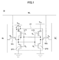
- Figure 1 is an equivalent circuit diagram of a typical SRAM 10.
- the SRAM 10 includes a first CMOS inverter I 1 in which a first load transistor LT 1 and a first driver transistor DT 1 are connected in series, a second CMOS inverter I 2 in which a second load transistor LT 2 and a second driver transistor LD 2 are connected in series.
- the first CMOS inverter I 1 and the second CMOS inverter I 2 form together a flip-flop circuit FF, wherein a node N 1 connecting the first load transistor LT 1 and the first driver transistor DT 1 with each other, is connected to a first bit line BL via a first transfer transistor TF 1 , while the first transfer transistor TF 1 is controlled by a word line WL.
- a node N 2 connecting the second load transistor LT2 and the second driver transistor DT 2 with each other is connected to a first bit line /BL via a second transfer transistor TF 2 controlled by the word line WL.
- a semiconductor memory device includes: a semiconductor substrate; a first CMOS inverter comprising first and second MOS transistors having respective, mutually different channel conductivity types and connected in series at a first node on said semiconductor substrate; a second CMOS inverter comprising third and fourth MOS transistors having respective, mutually different channel conductivity types and connected in series at a second node on said semiconductor substrate, said second CMOS inverter forming, together with said first CMOS inverter, a flip-flop circuit; a first transfer transistor provided on said semiconductor substrate between a first bit line and said first node, said first transfer transistor having a first gate electrode connected to a word line and driven by a selection signal on said word line; a second transfer transistor provided on said semiconductor substrate between a second bit line and said second node, said second transfer transistor having a second gate electrode connected to said word line and driven by a selection signal on said word line; a polysilicon resistance element formed on a device isolation region on said semiconductor substrate, each of
- a method for fabricating a semiconductor memory device said semiconductor memory device including: a first CMOS inverter comprising first and second MOS transistors having respective, mutually opposite channel conductivity types and connected in series at a first node on a semiconductor substrate; a second CMOS inverter comprising third and fourth MOS transistors having respective, mutually opposite channel conductivity types and connected in series at a second node on said semiconductor substrate, said second CMOS inverter forming, together with said first CMOS inverter, a flip-flop circuit; a first transfer transistor provided on said substrate between a first bit line and said first node, said first transfer transistor having a first gate electrode connected to a word line and driven by a selection signal on said word line; a second transfer transistor provided on said substrate between a second bit line and said second node, said second transfer transistor having a second gate electrode connected to said word line and driven by a selection signal on said word line; and a polysilicon resistance element formed on a device isolation region on
- a semiconductor memory device includes: a semiconductor substrate; a first CMOS inverter comprising first and second MOS transistors having respective, mutually opposite channel conductivity types and connected in series at a first node on said semiconductor substrate; a second CMOS inverter comprising third and fourth MOS transistors having respective, mutually opposite channel conductivity types and connected in series at a second node on said semiconductor substrate, said second CMOS inverter forming, together with said first CMOS inverter, a flip-clop circuit; a first transfer transistor provided on said semiconductor substrate between a first bit line and said first node, said first transfer transistor having a first gate electrode connected to a word line and driven by a selection signal on said word line; a second transfer transistor provided on said semiconductor substrate between a second bit line and said second node, said second transfer transistor having a second gate electrode connected to said word line and driven by a selection signal on said word line, said first MOS transistor being formed in a first device region of a band shape formed
- Figure 2A shows an SRAM layout corresponding to the equivalent circuit diagram of Figure 1 according to a related art of the present invention. Further, Figure 2B shows a cross-sectional diagram taken along a line A-A' of Figure 2A .
- n-type well 11N and a p-type well 11P on the surface of the silicon substrate 11 by an ion implantation process, wherein it can be seen that there are formed n-type device regions 11A 1 and 11A 2 in the n-type well 11N by a device isolation region 11I in a symmetric relationship. Further, in the p-type well 11P, there are formed p-type device regions 11B and 11C by the device isolation region 11I.
- load transistors LT 1 and LT 2 of Figure 1 in the form of a p-channel MOS transistor respectively, wherein the load transistor LT 1 has a p-type polysilicon gate electrode G 1 crossing the device region 11A 1 .
- the load transistor LT 2 has a p-type polysilicon gate electrode G 2 crossing the device region 11A 2 .
- a power contact V DD In a part of the n-type device region 11A 1 located at one side of the gate electrode G 1 , there is formed a power contact V DD . Further, there is formed a via-plug V 2 in the n-type device region 11A 1 at the other side of the gate electrode G 1 for connecting the polysilicon gate G 2 to the device region 11A 1 .
- a power contact V DD in a part of the n-type device region 11A 2 located at a one side of the gate electrode G 2 , there is formed a power contact V DD , while it can be seen that there is formed a via-plug V 4 in the n-type device region 11A 2 at the other side of the gate electrode G 2 for connecting the polysilicon gate G 1 to the device region 11A 2 .
- the device isolation region 11I defines the p-type device region 11B and that there is formed an n-channel MOS transistor having an n-type polysilicon gate electrode G 3 in a region of increased width of the p-type device region 11B as the driver transistor DT 1 . Further, there is formed an n-channel MOS transistor having an n-type polysilicon gate electrode G 4 in a part of the p-type device region 11B of narrow width as the transfer transistor TF 1 .
- the device isolation region 11I defines the p-type device region 11C and that there is formed an n-channel MOS transistor having an n-type polysilicon gate electrode G 5 in a region of increased width of the p-type device region 11C as the driver transistor DT 2 . Further, there is formed an n-channel MOS transistor having an n-type polysilicon gate electrode G 6 in a part of the p-type device region 11C of narrow width as the transfer transistor TF 2 .
- a via-contact V 1 in a part of the device region 11B between the gate electrodes G 3 and G 4 , wherein the via-contact V 1 is connected to the via-contact V 2 by way of a local interconnection pattern (not illustrated).
- a via-contact V 3 in a part of the device region 11C between the gate electrodes G 5 and G 6 , wherein the via-contact V 3 is connected to the via-contact V 4 by way of a local interconnection pattern (not illustrated).
- the via-contacts V 1 and V 2 constitute the node N 1 of Figure 1
- the via-contacts V 3 and V 4 constitute the node N 2 .
- a ground contact in a part of the p-type device region 11B at an opposite side of the via-contact V 1 with regard to the gate electrode G 2
- a via-contact V 5 connected to the bit line BL in a part of the p-type device region 11B at the opposite side of the via-contact V 1 with regard to the gate electrode G 4 .
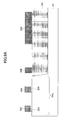
- the horizontal axis represents the gate voltage and the vertical axis represents the drain current, wherein it can be seen that a large drain current is attained with the experiment indicated by the numeral 2, while there is caused a decrease of drain current with the experiment indicated by the numeral 1 for the same gate voltage.
- the experiment designated with the numeral 1 represents the case shown in Figure 4A in which a supply voltage V DD is applied to the source side of the p-channel MOS transistor constituting the load transistor while grounding the drain side.
- the experiment designated with the numeral 2 represents the case shown in Figure 4B in which a supply voltage V DD is applied to the drain side of the same p-channel MOS transistor while grounding the source side.
- the fact that a small drain current is obtained in the experiment of Figure 3 designated by the numeral 1 and that a large drain current is obtained in the experiment designated by the numeral 2 indicates that there exists a resistance R at the source side of the load transistor as shown in Figures 4A and 4B .
- Figure 5A shows a plan view of the SRAM of Figure 2 for the part surrounded in Figure 2 by a broken line
- Figure 5B shows a cross-sectional diagram taken along a line A-A' of Figure 5A
- Figure 5C shows a cross-sectional diagram taken along a line B-B' of Figure 5A
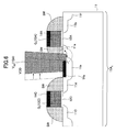
- Figure 6 is a diagram showing the part surrounded by the broken line in Figure 5B with enlarged scale.
- the n-type diffusion region 11A 1 is defined on the silicon substrate 11 by the device isolation region 11I, and the gate electrodes G 1 and G 7 extend across the n-type device region 11A 1 . Further, a power contact V DD is formed between the gate electrodes G 1 and G 7 . Further, the via-contact V 2 is formed in a manner to connect the gate electrode G 2 and the n-channel region 11A 1 .
- the gate electrodes G 1 , G 2 and G 7 are formed respectively in the form of polysilicon patterns 13A, 13B and 13C each doped to n-type, wherein each of the gate electrodes G 1 , G 2 and G 7 carries, on respective sidewall surfaces, sidewall insulation films SW of typically a silicon oxide film.
- the polysilicon patterns 13A and 13C are formed on the n-type device region 11A 1 via gate insulation films 12A and 12C, while the polysilicon pattern 13B is formed on the device isolation insulation film 11I.
- the device region 11A 1 there is formed a p-type source extension diffusion region 11a at one side of the gate electrode pattern 13A and a p-type drain extension diffusion region 11b is formed in the device region 11A 1 at an opposite side of the gate electrode pattern 13A.
- a p-type source extension diffusion region 11c at one side of the gate electrode pattern 13C and a p-type drain extension diffusion region 11d is formed in the device region 11A 1 at an opposite side of the gate electrode pattern 13C.
- a p + -type diffusion region 11e in a part between the gate electrode patterns 13A and 13C so as to be located at the respective outer sides of the sidewall insulation films SW as the source regions of the respective load transistors having the gate electrodes G 1 and G 7 .
- silicide layers 14A - 14C are formed on the respective surfaces of the polysilicon gate electrode patterns 13A - 13C, and silicide layers 14e and 14f are formed on the respective surfaces of the source region 11e and the drain region 11f.
- the polysilicon gate electrode patterns 13A - 13C, including the silicide layers 14A - 14C and the sidewall insulation films SW, are covered with an interlayer insulation film 15 formed on the silicon substrate 11, and a via-plug 15A constituting the via-contact V DD is contacted to the source region 11e via the silicide layer 14e. Further, a via-plug 15B constituting the via-contact V 2 makes a contact with the drain region 11f via the silicide layer 14f.
- the sidewall insulation film SW of the polysilicon gate electrode 13B at the side of the polysilicon gate electrode pattern 13A is removed, and with this, the via-plug 15B performs the function of connecting the polysilicon gate electrode pattern 14B to the drain region 11f electrically.
- the via-plug 15A has a diameter larger than the width of the device region 11A 1 when viewed in the cross-sectional view taken along the line B-B' of Figure 5A .
- the via-plugs 15A and 15B cause electrical contact with the source regions 11e and 11f via the silicide layers 14e and 14f, respectively.
- the source current is injected efficiently from the via-plug 15A into the source region 11e via the silicide layer 11e.
- the via-plug 15A may contact directly with the p-type diffusion region 11a as represented in Figure 5B by a small circle.
- Figure 6 shows the part of Figure 5B in the vicinity of the via-plug 15A with enlarged scale.
- the via-plug 15A has the tip end thereof invading into the p-type diffusion region 11a, and as a result, there is caused a restriction of carrier path from the p + -type source region 11e to the p-type source extension region 11a and further to the channel region right underneath the polysilicon gate electrode pattern 13A.
- the via-plug 15A is generally formed of a metal such as W (tungsten), wherein the surface thereof is covered by a metal such as Ta or Ti or a conductive nitride such as TiN.
- W tungsten
- the depletion layer extending from the surface of the via-plug 15A into the interior of the p - -type source region 11a restricts the carrier path further. It is believed that this is the cause of the source resistance explained with reference to Figure 3 and Figures 4A and 4B .
- Such a problem of misalignment of via-plug may be avoided by using the technology of so-called self-aligned contact that forms the sidewall insulation films SW with a material having resistance against the etching used for formation of the via-hole corresponding to the via-plug 15A.
- the SRAM having the layout of Figure 2
- the present invention provides a semiconductor memory device comprising: a semiconductor substrate; a first CMOS inverter comprising first and second MOS transistors having respective, mutually different channel conductivity types and connected in series at a first node on said semiconductor substrate; a second CMOS inverter comprising third and fourth MOS transistors having respective, mutually different channel conductivity types and connected in series at a second node on said semiconductor substrate, said second CMOS inverter forming, together with said first CMOS inverter, a flip-flop circuit; a first transfer transistor provided on said semiconductor substrate between a first bit line and said first node, said first transfer transistor having a first gate electrode connected to a word line and driven by a selection signal on said word line; a second transfer transistor provided on said semiconductor substrate between a second bit line and said second node, said second transfer transistor having a second gate electrode connected to said word line and driven by a selection signal on said word line; a polysilicon resistance element formed on a device isolation region on said semiconductor substrate
- the present invention provides a method for fabricating a semiconductor memory device, said semiconductor memory device comprising: a first CMOS inverter comprising first and second MOS transistors having respective, mutually opposite channel conductivity types and connected in series at a first node on a semiconductor substrate; a second CMOS inverter comprising third and fourth MOS transistors having respective, mutually opposite channel conductivity types and connected in series at a second node on said semiconductor substrate, said second CMOS inverter forming, together with said first CMOS inverter, a flip-flop circuit; a first transfer transistor provided on said substrate between a first bit line and said first node, said first transfer transistor having a first gate electrode connected to a word line and driven by a selection signal on said word line; a second transfer transistor provided on said substrate between a second bit line and said second node, said second transfer transistor having a second gate electrode connected to said word line and driven by a selection signal on said word line; and a polysilicon resistance element formed on a device isolation region
- the present invention provides a semiconductor memory device comprising: a semiconductor substrate; a first CMOS inverter comprising first and second MOS transistors having respective, mutually opposite channel conductivity types and connected in series at a first node on said semiconductor substrate; a second CMOS inverter comprising third and fourth MOS transistors having respective, mutually opposite channel conductivity types and connected in series at a second node on said semiconductor substrate, said second CMOS inverter forming, together with said first CMOS inverter, a flip-clop circuit; a first transfer transistor provided on said semiconductor substrate between a first bit line and said first node, said first transfer transistor having a first gate electrode connected to a word line and driven by a selection signal on said word line; a second transfer transistor provided on said semiconductor substrate between a second bit line and said second node, said second transfer transistor having a second gate electrode connected to said word line and driven by a selection signal on said word line, said first MOS transistor being formed in a first device region of a band
- the problem of increase of source resistance is avoided even in the case there is caused positional offset of power contact in the load transistor that constitutes the SRAM, and it becomes possible to avoid occurrence of defects.
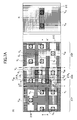
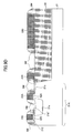
- Figure 7A shows the layout of an SRAM 20 according to a first embodiment. Further, Figure 7B shows a cross-sectional diagram taken along a line A-A' of Figure 7A .
- the SRAM 20 is formed on a silicon substrate 21 and has a construction to form an equivalent circuit diagram identical to that shown in Figure 1 .
- n-type well 21N and a p-type well 21P on the surface of the silicon substrate 21 by an ion implantation process, wherein there are formed n-type device regions 21A 1 and 21A 2 in the n-type well 21N by a device isolation region 21I in point symmetry. Further, in the p-type well 21P, there are formed p-type device regions 21B and 21C by the device isolation region 21I.
- load transistors LT 1 and LT 2 of Figure 1 in the form of a p-channel MOS transistor, respectively, wherein the load transistor LT 1 has a p-type polysilicon gate electrode G1 crossing the device region 21A 1 , while the load transistor LT 2 has a p-type polysilicon gate electrode G 2 traversing the device region 21A 2 .
- a power contact V DD In a part of the n-type device region 11A 1 located at one side of the gate electrode G 1 , there is formed a power contact V DD , while it can be seen that there is formed a via-plug V 2 in the n-type device region 21A 1 at the other side of the gate electrode G 1 for connecting the polysilicon gate G 2 to the device region 21A 1 .
- a power contact V DD in a part of the n-type device region 21A 2 located at a one side of the gate electrode G 2 , there is formed a power contact V DD , while it can be seen that there is formed a via-plug V 4 in the n-type device region 11A 2 at the other side of the gate electrode G 2 for connecting the polysilicon gate G 1 to the device region 21A 2 .
- the device isolation region 21I defines the p-type device region 21B and that there is formed an n-channel MOS transistor having an n-type polysilicon gate electrode G 3 in a region of increased width of the p-type device region 11B as the driver transistor DT 1 . Further, there is formed an n-channel MOS transistor having an n-type polysilicon gate electrode G 4 in a part of the p-type device region 21B of narrow width as the transfer transistor TF 1 .
- the device isolation region 21I defines the p-type device region 21C and that there is formed an n-channel MOS transistor having an n-type polysilicon gate electrode G 5 in a region of increased width of the p-type device region 21C as the driver transistor DT 2 . Further, there is formed an n-channel MOS transistor having an n-type polysilicon gate electrode G 6 in a part of the p-type device region 21C of narrow width as the transfer transistor TF 2 .
- a via-contact V 1 in a part of the device region 21B between the gate electrodes G 3 and G 4 , wherein the via-contact V 1 is connected to the via-contact V 2 by way of a local interconnection pattern (not illustrated).
- a via-contact V 3 in a part of the device region 21C between the gate electrodes G 5 and G 6 , wherein the via-contact V 3 is connected to the via-contact V 4 by way of a local interconnection pattern (not illustrated).
- the via-contacts V 1 and V 2 constitute the node N 1 of Figure 1
- the via-contacts V 3 and V 4 constitute the node N 2 .
- a ground contact in a part of the p-type device region 21B at an opposite side of the via-contact V 2 with regard to the gate electrode G 2
- a via-contact v 5 connected to the bit line BL in a part of the p-type device region 11B at the opposite side of the via-contact V 1 with regard to the gate electrode G 4 .
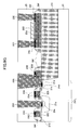
- Figure 8 shows a cross-sectional diagram taken along the line B-B' .
- the gate electrodes G 1 , G 2 and G 7 are formed respectively in the form of polysilicon patterns 23A, 23B and 23C each doped to n-type, wherein each of the gate electrodes G 1 , G 2 and G 7 carries, on respective sidewall surfaces, sidewall insulation films SW of typically a silicon oxide film.
- the polysilicon patterns 23A and 23C are formed on the n-type device region 21A 1 via gate insulation films 22A and 22C, while the polysilicon pattern 23B is formed on the device isolation insulation film 21I.
- a p + -type diffusion region 21a is formed in the device region 21A 1 at one side of the gate electrode pattern 23A as the source region, and there is formed a p-type diffusion region 21b at the other side as the drain extension region.
- a p-type diffusion region 21c is formed in the device region 21A 1 at one side of the gate electrode pattern 23C as the drain extension region, the p + -type diffusion region 21a is formed as a common source region at the other side.
- a drain region 21d of a p + -type diffusion region at the opposite side of the source region 21a with regard to the gate electrode pattern 23A at a location between the sidewall insulation film SW and the device isolation insulation film 21I.
- silicide layers 24A - 24C are formed on the respective surfaces of the polysilicon gate electrode patterns 23A - 23C, and silicide layers 24a and 24d are formed on the respective surfaces of the source region 21a and the drain region 21d.
- an interlayer insulation film 25 so as to cover the polysilicon gate electrode patterns 23A - 23C including the silicide layers 24A - 24C and the sidewall insulation films SW, wherein the interlayer insulation film 25 is formed with a via-plug 25A constituting the via-contact V DD in correspondence to the source region 21a such that the via-plug 25A makes a contact thereto via the silicide layer 24a.
- the interlayer insulation film 25 is formed with a via-plug 25B constituting the via-contact V 2 in correspondence to the drain region 21d such that the via-plug 25B makes a contact thereto via the silicide layer 24d.
- the sidewall insulation film SW of the polysilicon gate electrode 23B at the side of the polysilicon gate electrode pattern 23A is removed, and with this, the via-plug 25B performs the function of connecting the polysilicon gate electrode pattern 23B to the drain region 21d electrically.
- a polysilicon pattern 23D on another part of the same device isolation region 21I on the same silicon substrate 21 as a polysilicon resistance element R, and the interlayer insulation film 25 is formed with via-plugs 25E and 25F so as to make a contact with the polysilicon pattern 23D via respective silicide layers 24e and 24f.
- the polysilicon pattern 23D is formed simultaneously to the polysilicon gate patterns 23A - 23C and is formed with the sidewall insulation films SW similarly. Further, with the illustrated example, it can be seen that there is left a dielectric pattern 25d, which is used for the mask at the time of formation of the silicide layers 24e and 24f, on the polysilicon pattern 23D.
- the polysilicon pattern 23D constituting the resistance element R is formed simultaneously to the polysilicon gate electrode patterns 23A - 23C as a result of patterning of the same polysilicon film, and thus, the polysilicon pattern 23D has the same film thickness, and hence the same height, to each of the polysilicon gate electrode patterns 23A - 23D. Further, the polysilicon pattern 23D is doped by the same impurity element to the same concentration level as in the case the polysilicon gate electrode patterns 23A - 23D.
- the polysilicon patterns 23A - 23D are formed on the silicon substrate 21 as a result of patterning of a polysilicon film (not shown), such that the polysilicon patterns 23A and 23C are formed on the device region 21A 1 respectively via gate insulation films 22A and 22C, and such that the polysilicon pattern 23B and 23D are formed on the device isolation insulation film 21I that defines the device region 21A 1 .
- the polysilicon pattern 23D used to form the resistance element R is carried upon the device isolation insulation film 21I that also carries thereon the polysilicon pattern 23B.
- the device region 21A 1 is covered with a resist pattern R except for the part located between the polysilicon pattern 23A and the polysilicon pattern 23B, and B+ ions are injected into the part of the device region 21A 1 not covered with the resist pattern R by an ion implantation process conducted under an acceleration voltage of 8keV with a dose of 4.0 ⁇ 10 15 cm -2 .
- the p + -type diffusion region 21a is formed in the device region 21A 1 between the polysilicon patterns 23A and 23C.
- the polysilicon patterns 21A - 21C and the polysilicon pattern 23D on the device isolation insulation film 21I are doped with B to p + -type.
- the resist pattern R is removed, and ion implantation of B+ is conducted into the device region 21A 1 while using the polysilicon patterns 23A and 23C as a mask.
- ion implantation of B+ is conducted into the device region 21A 1 while using the polysilicon patterns 23A and 23C as a mask.
- a similar injected region 21b' is formed in a surface part of the source region 21a in overlapping therewith.
- an insulation film (not shown) is deposited on the structure of Figure 9C by a CVD process, followed by an etchback process conducted by an anisotropic etching process that works generally perpendicularly to the substrate surface.
- sidewall insulation films SW are formed on the respective sidewall surfaces of the polysilicon patterns 23A - 23D.
- the device region 21A 1 is introduced with B+ by an ion implantation process while using the polysilicon patterns 21A and 21C as a mask.
- the p + -type drain region 21d is formed between the polysilicon pattern 23A and the device isolation insulation film 21I carrying the polysilicon pattern 23B at the part outside of the sidewall insulation film SW. Further, similar ion implantation of B is conducted also into the interior of the p + -type source region 21a, and there is formed a p+-type ion implantation region 21d' in overlapping with the p + -type source region 21a.
- the ion implantation of B is conducted to the polysilicon patterns 23A - 23D under the same condition.
- a silicide layer is formed on the exposed silicon surface of the structure of Figure 9E by a salicide process, and as a result, there are formed silicide layers 24A - 24C on the polysilicon patterns 23A - 23C respectively. Further, silicide layers 21a and 24d are formed on the source region 21a and the drain region 21d. Further, in the polysilicon pattern 23D constituting the resistance element R, there are formed two silicide formation regions in separation from each other by a dielectric pattern 25d, and the silicide layers 24e and 24f are formed on such silicide formation regions.
- step of Figure 9G there are formed via-holes exposing the silicide layers 24e and 24f of the polysilicon pattern 23D in the interlayer insulation film 25, and the resistance element R of the polysilicon pattern 23D is formed simultaneously by filling the via-holes with the via-plugs 25D and 25E.
- Figure 9G shows the state in which there is no positional offset in the via-plugs 25A and 25B, while even in the case the via-plugs 25A and 25B are displaced in the direction to the polysilicon patterns 23A and 23B as shown in Figure 9H , the via-plug 25A maintains the contact to the high-concentration diffusion region 21a, and there arises no increase of source resistance in the load transistor that uses the polysilicon pattern 23A as the gate electrode. Thus, there arises no problem of change of transistor characteristics explained previously with reference to Figure 3 .
- Figure 10 is a diagram extracting the n-well part including the device regions 11A 1 and 11A 2 from the layout of Figure 2 .
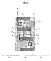
- Figure 11 is a diagram showing the layout of an SRAM according to a second embodiment.
- those parts explained before are designated by the same reference numerals and the description thereof will be omitted.
- the present embodiment does not increase the width of the device regions 11A 1 and 11A 2 in correspondence to he via-contact V DD as in the case of the layout of Figure 10 but displaces the via-contact V DD in one direction.
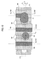
- Figure 12 shows the device region 11A 1 of Figure 11 in a plan view.
- each of the polysilicon pattern 13C that corresponds to the gate electrode G 7 , the polysilicon pattern 13A that corresponds to the gate electrode G 1 and the polysilicon pattern 13B that corresponds to the gate electrode G 2 carries the sidewall insulation films SW thereon and extends across the device region 11A 1 , wherein it can be seen that the via-plug 15A constituting the via-contact V DD is formed between the polysilicon pattern 13A and 13C such that the via-plug 15A is located between a pair of the sidewall insulation films SW.
- the sidewall insulation film SW is removed locally at the side of the polysilicon pattern 13B facing the polysilicon pattern 14A, and the via-plug 15B constituting the via-contact V 2 connects the polysilicon pattern 13B to the device region 11A 1 .
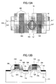
- Figure 13A is a plan view extracting a part of Figure 12 in the vicinity of the via-contact V DD , and hence the contact plug 15A
- Figure 13B is a cross-sectional diagram taken along a line bx1-bx1' shown in Figure 13A
- Figure 13C is a cross-sectional diagram taken along a line bx2-bx2' in Figure 13A
- Figure 13D is a cross-sectional diagram taken along a line by1-by1' in Figure 13A .
- the via-plug 15A has a diameter W 1 larger than the width W 2 of the device region 11A1 (W 1 >W 2 ) as shown in the cross-section of Figure 13D .
- the part of the device regions 11A 1 and 11A 2 in Figures 11 and 12 is covered with a silicide film except for the parts covered by the via-plugs 15A and 15B that the via-contacts V DD and V 2 or by the polysilicon patterns 13A-13C constituting the gate electrodes G 1 , G 2 and G 7 including the sidewall insulation films SW thereof.
- Figure 14 is a diagram showing the layout of an SRAM according to a third embodiment.
- those parts explained before are designated by the same reference numerals and the description thereof will be omitted.
- the present embodiment displaces one of the via-contacts V DD in one direction similarly to the layout of Figure 11 and further expands the width of the device region 11A1 at the part where the via-contact V DD is formed in a direction away from the adjacent p-type well.
- the diameter W 1 of the via-plug 15A is larger than the width W 2 of the device region 11A 1 (W 1 >W 2 ), while it is possible to secure a width of about 30nm for the carrier path circumventing the via-plug 15A by expanding the width of the device region 11A 1 by about 40nm and displacing the central line c 2 of the via-plug 15A by 25nm with regard to the central line c1 of the device region 11A 1 .
- the part of the device regions 11A 1 and 11A 2 in Figure 14 is covered with a silicide film except for the parts covered by the via-plugs 15A and 15B that the via-contacts V DD and V 2 or by the polysilicon patterns 13A-13C constituting the gate electrodes G 1 , G 2 and G 7 including the sidewall insulation films SW thereof.
- the problem of increase of the source resistance associated with displacement of the contact is successfully avoided by securing the circumventing path of carriers around the via-contact V DD .
- sufficient effect is attained when such a circumventing path is provided with the width of 10-30nm.
- the conductivity type of p-type and n-type can be reversed in each of the foregoing embodiments.
- CoSi 2 or NiSi can used for the silicide layer.
Landscapes
- Engineering & Computer Science (AREA)
- Microelectronics & Electronic Packaging (AREA)
- Computer Hardware Design (AREA)
- Semiconductor Memories (AREA)
- Internal Circuitry In Semiconductor Integrated Circuit Devices (AREA)
- Semiconductor Integrated Circuits (AREA)
Abstract
Description
- The present application is based on Japanese priority application No.
2007-042498 filed on February 22, 2007 - The present invention generally relates to semiconductor devices and more particularly to a semiconductor memory device that includes a static random access memory.
- A static random access memory (referred to hereinafter as SRAM) is a high-speed semiconductor memory device including a transfer transistor selected by a word line and two CMOS inverters forming together a flip-flop connection, wherein each of the CMOS inverters is connected to a corresponding bit line via a corresponding transfer transistor. SRAMs are used extensively in high-speed logic circuit devices together with high-speed logic elements such as CMOS circuit.
-
Figure 1 is an equivalent circuit diagram of atypical SRAM 10. - Referring to
Figure 1 , the SRAM 10 includes a first CMOS inverter I1 in which a first load transistor LT1 and a first driver transistor DT1 are connected in series, a second CMOS inverter I2 in which a second load transistor LT2 and a second driver transistor LD2 are connected in series. The first CMOS inverter I1 and the second CMOS inverter I2 form together a flip-flop circuit FF, wherein a node N1 connecting the first load transistor LT1 and the first driver transistor DT1 with each other, is connected to a first bit line BL via a first transfer transistor TF1, while the first transfer transistor TF1 is controlled by a word line WL. Similarly, a node N2 connecting the second load transistor LT2 and the second driver transistor DT2 with each other, is connected to a first bit line /BL via a second transfer transistor TF2 controlled by the word line WL. - In SRAMs of such a construction, current drivability of the load transistors LT1 and LT2 that drive the driver transistors DT1 and DT2 is extremely important for attaining high-speed operation of the SRAM.
-
Patent Reference 1 Japanese Laid-Open Patent Application2006-41035 -
Patent Reference 2 Japanese Laid-Open Patent Application7-131003 - Patent Reference 3 Japanese Laid-Open Patent Application
7-169858 - Patent Reference 4 Japanese Laid-Open Patent Application
2002-329798 - Patent Reference 5 Japanese Laid-Open Patent Application
2002-190534 - According to an aspect of an embodiment, a semiconductor memory device includes: a semiconductor substrate; a first CMOS inverter comprising first and second MOS transistors having respective, mutually different channel conductivity types and connected in series at a first node on said semiconductor substrate; a second CMOS inverter comprising third and fourth MOS transistors having respective, mutually different channel conductivity types and connected in series at a second node on said semiconductor substrate, said second CMOS inverter forming, together with said first CMOS inverter, a flip-flop circuit; a first transfer transistor provided on said semiconductor substrate between a first bit line and said first node, said first transfer transistor having a first gate electrode connected to a word line and driven by a selection signal on said word line; a second transfer transistor provided on said semiconductor substrate between a second bit line and said second node, said second transfer transistor having a second gate electrode connected to said word line and driven by a selection signal on said word line; a polysilicon resistance element formed on a device isolation region on said semiconductor substrate, each of said first and third MOS transistors being formed in a device region of a first conductivity type defined in said semiconductor substrate by said device isolation region, each of said first and third MOS transistors including: a polysilicon gate electrode formed on said semiconductor substrate via a gate insulation film and having gate sidewall insulation films at respective sidewall surfaces thereof; a second conductivity type source region formed in said semiconductor substrate at a first side of said polysilicon gate electrode such that an end part of said second conductivity type source region invades into a part of said semiconductor substrate right underneath said polysilicon gate electrode; a second conductivity type drain extension region formed in a surface part of said semiconductor substrate at a second side opposite to said first side of said polysilicon gate electrode such that an end part of said second conductivity type drain extension region invades into a part of said semiconductor substrate right underneath said polysilicon gate electrode; and a second conductivity type drain region formed in said semiconductor substrate at an outer side of said gate sidewall insulation film of said second side in overlapping with said drain extension region with a depth larger than a depth of said second conductivity type drain extension region, said source region being formed deeper than said drain extension region, said polysilicon gate electrode having a film thickness identical to a film thickness of said polysilicon resistance element, said source region and said polysilicon resistance element being doped with the same dopant element.
- According to another aspect of an embodiment, a method for fabricating a semiconductor memory device, said semiconductor memory device including: a first CMOS inverter comprising first and second MOS transistors having respective, mutually opposite channel conductivity types and connected in series at a first node on a semiconductor substrate; a second CMOS inverter comprising third and fourth MOS transistors having respective, mutually opposite channel conductivity types and connected in series at a second node on said semiconductor substrate, said second CMOS inverter forming, together with said first CMOS inverter, a flip-flop circuit; a first transfer transistor provided on said substrate between a first bit line and said first node, said first transfer transistor having a first gate electrode connected to a word line and driven by a selection signal on said word line; a second transfer transistor provided on said substrate between a second bit line and said second node, said second transfer transistor having a second gate electrode connected to said word line and driven by a selection signal on said word line; and a polysilicon resistance element formed on a device isolation region on said semiconductor substrate, said method includes the steps of: forming a first polysilicon pattern constituting a gate electrode of said first MOS transistor on a device region of a first conductivity type defined on said semiconductor substrate by said device isolation region via a gate insulation film, simultaneously with a second polysilicon pattern constituting said polysilicon resistance element on said device isolation region, as a result of patterning of a polysilicon film; introducing an impurity element of said second conductivity type into said device region at a first side of said first polysilicon pattern and further into said second polysilicon pattern such that there is formed a source region of said second conductivity type at said first side of said first polysilicon pattern in said device region and doping said second polysilicon pattern with said impurity element; introducing an impurity element of said second conductivity type into said device region at said first side and at a second side opposite to said first side of said first polysilicon pattern and further into said second polysilicon pattern such that there is formed a drain extension region in a surface part of said device region at said second side of said first polysilicon pattern with an impurity concentration lower than an impurity concentration of said source region and increasing an impurity concentration of said second polysilicon pattern; forming sidewall insulation films on respective sidewall surfaces of said first and second polysilicon patterns; and introducing an impurity element of said second conductivity type into said device region and further into said second polysilicon pattern while using said first polysilicon pattern and said sidewall insulation films at said first side and said second side of said first polysilicon pattern as a mask such that there are formed drain regions of said second conductivity type at respective outer parts of said sidewall insulation films of said first side and said second side of said first polysilicon pattern and such that an impurity concentration of said second polysilicon pattern is increased.
- According to further another aspect of an embodiment, a semiconductor memory device includes: a semiconductor substrate; a first CMOS inverter comprising first and second MOS transistors having respective, mutually opposite channel conductivity types and connected in series at a first node on said semiconductor substrate; a second CMOS inverter comprising third and fourth MOS transistors having respective, mutually opposite channel conductivity types and connected in series at a second node on said semiconductor substrate, said second CMOS inverter forming, together with said first CMOS inverter, a flip-clop circuit; a first transfer transistor provided on said semiconductor substrate between a first bit line and said first node, said first transfer transistor having a first gate electrode connected to a word line and driven by a selection signal on said word line; a second transfer transistor provided on said semiconductor substrate between a second bit line and said second node, said second transfer transistor having a second gate electrode connected to said word line and driven by a selection signal on said word line, said first MOS transistor being formed in a first device region of a band shape formed on said semiconductor substrate by a device isolation region, said first MOS transistor having a gate electrode of a first polysilicon pattern traversing said first device region, said third MOS transistor being formed in a second device region of a band shape formed on said semiconductor substrate by said device isolation region, said third MOS transistor having a gate electrode of a second polysilicon pattern traversing said second device region, said first polysilicon pattern being connected to a first end part of said second device region by a first via-plug, said second polysilicon pattern being connected to a first end of said first device region by a second via-plug, a third via-plug being in contact with a part of said first device region at a side opposite to a side of said first via-plug with regard to said first polysilicon pattern as a power contact, a fourth via-plug being in contact to a part of said second device region at a side opposite to said second via-plug with regard to said second polysilicon pattern as a power contact, said third via-plug having a diameter larger than a width of said first device region, said fourth via-plug having a diameter larger than a width of said second device region, said third via-plug being offset from a central line of said first device region, said fourth via-plug being offset from a central line of said second device region.
-
-
Figure 1 is a diagram showing an equivalent circuit diagram of SRAM; -
Figures 2A and2B are diagrams explaining the construction of an SRAM according to a related art; -
Figure 3 is a diagram explaining the problems to be solved; -
Figures 4A and 4B are further diagrams explaining the problems to be solved; -
Figures 5A - 5C are further diagrams explaining the problems to be solved; -
Figure 6 is a further diagram explaining the problems to be solved; -
Figures 7A and7B are diagrams explaining the construction of an SRAM according to a first embodiment; -
Figure 8 is a cross-sectional diagram showing the construction of the SRAM ofFigures 7A and7B in detail; -
Figures 9A - 9H are diagrams explaining the fabrication process of an SRAM ofFigure 8 ; -
Figure 10 is a diagram explaining the problems to be solved; -
Figure 11 is a diagram showing the construction of an SRAM according to a second embodiment; -
Figure 12 is a diagram showing the construction of an SRAM according to a second embodiment; -
Figures 13A - 13D are diagrams showing the construction of the SRAM according to the second embodiment; -
Figure 14 is a diagram showing the construction of an SRAM according to a third embodiment; -
Figure 2A shows an SRAM layout corresponding to the equivalent circuit diagram ofFigure 1 according to a related art of the present invention. Further,Figure 2B shows a cross-sectional diagram taken along a line A-A' ofFigure 2A . - Referring to
Figures 2A and2B , there are formed an n-type well 11N and a p-type well 11P on the surface of thesilicon substrate 11 by an ion implantation process, wherein it can be seen that there are formed n-type device regions type well 11N by adevice isolation region 11I in a symmetric relationship. Further, in the p-type well 11P, there are formed p-type device regions device isolation region 11I. - In the
device regions Figure 1 in the form of a p-channel MOS transistor respectively, wherein the load transistor LT1 has a p-type polysilicon gate electrode G1 crossing thedevice region 11A1. Likewise, the load transistor LT2 has a p-type polysilicon gate electrode G2 crossing thedevice region 11A2. - In a part of the n-
type device region 11A1 located at one side of the gate electrode G1, there is formed a power contact VDD. Further, there is formed a via-plug V2 in the n-type device region 11A1 at the other side of the gate electrode G1 for connecting the polysilicon gate G2 to thedevice region 11A1. - Similarly, in a part of the n-
type device region 11A2 located at a one side of the gate electrode G2, there is formed a power contact VDD, while it can be seen that there is formed a via-plug V4 in the n-type device region 11A2 at the other side of the gate electrode G2 for connecting the polysilicon gate G1 to thedevice region 11A2. - Further, in the p-
type well 11P located at the left side of the n-type well 11N, it can be seen that thedevice isolation region 11I defines the p-type device region 11B and that there is formed an n-channel MOS transistor having an n-type polysilicon gate electrode G3 in a region of increased width of the p-type device region 11B as the driver transistor DT1. Further, there is formed an n-channel MOS transistor having an n-type polysilicon gate electrode G4 in a part of the p-type device region 11B of narrow width as the transfer transistor TF1. - Similarly, in the p-
type well 11P located at the right side of the n-type well 11N, it can be seen that thedevice isolation region 11I defines the p-type device region 11C and that there is formed an n-channel MOS transistor having an n-type polysilicon gate electrode G5 in a region of increased width of the p-type device region 11C as the driver transistor DT2. Further, there is formed an n-channel MOS transistor having an n-type polysilicon gate electrode G6 in a part of the p-type device region 11C of narrow width as the transfer transistor TF2. - Further, there is formed a via-contact V1 in a part of the
device region 11B between the gate electrodes G3 and G4, wherein the via-contact V1 is connected to the via-contact V2 by way of a local interconnection pattern (not illustrated). Similarly, there is formed a via-contact V3 in a part of thedevice region 11C between the gate electrodes G5 and G6, wherein the via-contact V3 is connected to the via-contact V4 by way of a local interconnection pattern (not illustrated). Here, the via-contacts V1 and V2 constitute the node N1 ofFigure 1 , while the via-contacts V3 and V4 constitute the node N2. - Further, there is formed a ground contact in a part of the p-
type device region 11B at an opposite side of the via-contact V1 with regard to the gate electrode G2, and there is formed a via-contact V5 connected to the bit line BL in a part of the p-type device region 11B at the opposite side of the via-contact V1 with regard to the gate electrode G4. Similarly, there is formed a ground contact Vss in a part of the p-type device region 11C at an opposite side of the via-contact V3 with regard to the gate electrode G5, and there is formed a via-contact V6 connected to the bit line /BL in a part of the p-type device region 11C at the opposite side of the via-contact V3 with regard to the gate electrode G6. - Further, with the layout of
Figure 2 , there is formed a gate electrode G7 of a different memory cell across the n-type device region 11A1. - Meanwhile, the inventor of the present invention has obtained interesting results shown in
Figure 3 as a result of analysis of the characteristics of the load transistor in a single bit defective part of the SRAM of such a construction. - Referring to
Figure 3 , the horizontal axis represents the gate voltage and the vertical axis represents the drain current, wherein it can be seen that a large drain current is attained with the experiment indicated by thenumeral 2, while there is caused a decrease of drain current with the experiment indicated by thenumeral 1 for the same gate voltage. - Here, the experiment designated with the
numeral 1 represents the case shown inFigure 4A in which a supply voltage VDD is applied to the source side of the p-channel MOS transistor constituting the load transistor while grounding the drain side. On the other hand, the experiment designated with thenumeral 2 represents the case shown inFigure 4B in which a supply voltage VDD is applied to the drain side of the same p-channel MOS transistor while grounding the source side. The fact that a small drain current is obtained in the experiment ofFigure 3 designated by thenumeral 1 and that a large drain current is obtained in the experiment designated by thenumeral 2 indicates that there exists a resistance R at the source side of the load transistor as shown inFigures 4A and 4B . In the case ofFigure 4A , the existence of the resistance R at the source side, to which the supply voltage VDD is applied, induces a decrease of the voltage VGS applied effectively across the source and drain, while this tends to lead to incomplete conduction of the transistor. In the case ofFigure 4B , on the other hand, there exists no such a resistance at the source side and there is caused no voltage drop in the source-gate voltage as a result of the resistance R. - In the equivalent circuit diagram, such a resistance R is thought to be formed in the part circled in the drawing by a broken line.
-
Figure 5A shows a plan view of the SRAM ofFigure 2 for the part surrounded inFigure 2 by a broken line, whileFigure 5B shows a cross-sectional diagram taken along a line A-A' ofFigure 5A . Further,Figure 5C shows a cross-sectional diagram taken along a line B-B' ofFigure 5A . Further,Figure 6 is a diagram showing the part surrounded by the broken line inFigure 5B with enlarged scale. - Referring to
Figure 5A , it can be seen that the n-type diffusion region 11A1 is defined on thesilicon substrate 11 by thedevice isolation region 11I, and the gate electrodes G1 and G7 extend across the n-type device region 11A1. Further, a power contact VDD is formed between the gate electrodes G1 and G7. Further, the via-contact V2 is formed in a manner to connect the gate electrode G2 and the n-channel region 11A1. - As shown in the cross-sectional diagram of
Figure 5B , the gate electrodes G1, G2 and G7 are formed respectively in the form ofpolysilicon patterns - In the cross-sectional diagram of
Figure 5B , thepolysilicon patterns type device region 11A1 viagate insulation films isolation insulation film 11I. - In the
device region 11A1, there is formed a p-type sourceextension diffusion region 11a at one side of thegate electrode pattern 13A and a p-type drainextension diffusion region 11b is formed in thedevice region 11A1 at an opposite side of thegate electrode pattern 13A. Similarly, there is formed a p-type sourceextension diffusion region 11c at one side of thegate electrode pattern 13C and a p-type drainextension diffusion region 11d is formed in thedevice region 11A1 at an opposite side of thegate electrode pattern 13C. - Further, in the n-
type device region 11A1, there is formed a p+-type diffusion region 11e in a part between thegate electrode patterns - Further, in the n-
type device region 11A1, there is formed adrain region 11f of similar p+-type diffusion region at the opposite side of thesource region 11e with regard to thegate electrode pattern 13A so as to be located between the sidewall insulation film SW and the deviceisolation insulation film 11I. - Further, there are formed
silicide layers 14A - 14C on the respective surfaces of the polysilicongate electrode patterns 13A - 13C, andsilicide layers source region 11e and thedrain region 11f. - Further, the polysilicon
gate electrode patterns 13A - 13C, including the silicide layers 14A - 14C and the sidewall insulation films SW, are covered with aninterlayer insulation film 15 formed on thesilicon substrate 11, and a via-plug 15A constituting the via-contact VDD is contacted to thesource region 11e via thesilicide layer 14e. Further, a via-plug 15B constituting the via-contact V2 makes a contact with thedrain region 11f via thesilicide layer 14f. Thereby, it should be noted that the sidewall insulation film SW of the polysilicon gate electrode 13B at the side of the polysilicongate electrode pattern 13A is removed, and with this, the via-plug 15B performs the function of connecting the polysilicongate electrode pattern 14B to thedrain region 11f electrically. - Further, with reference to
Figure 5C , it will be noted that, because of the extreme miniaturization of the SRAM of the present invention, the via-plug 15A has a diameter larger than the width of thedevice region 11A1 when viewed in the cross-sectional view taken along the line B-B' ofFigure 5A . - Now, in the case the via-
plugs 15A and 15B are formed at the respective, predetermined or nominal positions, the via-plugs 15A and 15B cause electrical contact with thesource regions plug 15A into thesource region 11e via thesilicide layer 11e. In the case there is caused a positional offset in the via-plugs 15A and 15B as shown in Figure 15B by the continuous lines, on the other hand, there is a concern that the via-plug 15A may contact directly with the p-type diffusion region 11a as represented inFigure 5B by a small circle. -
Figure 6 shows the part ofFigure 5B in the vicinity of the via-plug 15A with enlarged scale. - Referring to
Figure 6 , it can be seen that the via-plug 15A has the tip end thereof invading into the p-type diffusion region 11a, and as a result, there is caused a restriction of carrier path from the p+-type source region 11e to the p-typesource extension region 11a and further to the channel region right underneath the polysilicongate electrode pattern 13A. The via-plug 15A is generally formed of a metal such as W (tungsten), wherein the surface thereof is covered by a metal such as Ta or Ti or a conductive nitride such as TiN. Thus, the depletion layer extending from the surface of the via-plug 15A into the interior of the p--type source region 11a restricts the carrier path further. It is believed that this is the cause of the source resistance explained with reference toFigure 3 andFigures 4A and 4B . - When such a source resistance appears in one of the load transistors constituting an SRAM at the location shown by the broken line in
Figure 1 , for example, there is caused instability in the operation of the SRAM, while this leads to formation of defective memory cell. - Such a problem of misalignment of via-plug may be avoided by using the technology of so-called self-aligned contact that forms the sidewall insulation films SW with a material having resistance against the etching used for formation of the via-hole corresponding to the via-
plug 15A. In the case of the SRAM having the layout ofFigure 2 , however, there is a need of removing one of the sidewall insulation films of the polysilicon gate electrode G2 as shown inFigure 5B , and thus, it is difficult to construct the sidewall insulation films with a material having etching resistance. - In a first aspect, the present invention provides a semiconductor memory device comprising: a semiconductor substrate; a first CMOS inverter comprising first and second MOS transistors having respective, mutually different channel conductivity types and connected in series at a first node on said semiconductor substrate; a second CMOS inverter comprising third and fourth MOS transistors having respective, mutually different channel conductivity types and connected in series at a second node on said semiconductor substrate, said second CMOS inverter forming, together with said first CMOS inverter, a flip-flop circuit; a first transfer transistor provided on said semiconductor substrate between a first bit line and said first node, said first transfer transistor having a first gate electrode connected to a word line and driven by a selection signal on said word line; a second transfer transistor provided on said semiconductor substrate between a second bit line and said second node, said second transfer transistor having a second gate electrode connected to said word line and driven by a selection signal on said word line; a polysilicon resistance element formed on a device isolation region on said semiconductor substrate, each of said first and third MOS transistors being formed in a device region of a first conductivity type defined in said semiconductor substrate by said device isolation region, each of said first and third MOS transistors comprising: a polysilicon gate electrode formed on said semiconductor substrate via a gate insulation film and carrying gate sidewall insulation films at respective sidewall surfaces thereof; a second conductivity type source region formed in said semiconductor substrate at a first side of said polysilicon gate electrode such that an end part of said second conductivity type source region invades into a part of said semiconductor substrate right underneath said polysilicon gate electrode; a second conductivity type drain extension region formed in a surface part of said semiconductor substrate at a second side opposite to said first side of said polysilicon gate electrode such that an end part of said second conductivity type drain extension region invades into a part of said semiconductor substrate right underneath said polysilicon gate electrode; and a second conductivity type drain region formed in said semiconductor substrate at an outer side of said gate sidewall insulation film of said second side in overlapping with said drain extension region with a depth larger than a depth of said second conductivity type drain extension region, wherein said source region is formed deeper than said drain extension region, said polysilicon gate electrode having a film thickness identical to a film thickness of said polysilicon resistance element, said source region and said polysilicon resistance element being doped with the same dopant element.
- In another aspect, the present invention provides a method for fabricating a semiconductor memory device, said semiconductor memory device comprising: a first CMOS inverter comprising first and second MOS transistors having respective, mutually opposite channel conductivity types and connected in series at a first node on a semiconductor substrate; a second CMOS inverter comprising third and fourth MOS transistors having respective, mutually opposite channel conductivity types and connected in series at a second node on said semiconductor substrate, said second CMOS inverter forming, together with said first CMOS inverter, a flip-flop circuit; a first transfer transistor provided on said substrate between a first bit line and said first node, said first transfer transistor having a first gate electrode connected to a word line and driven by a selection signal on said word line; a second transfer transistor provided on said substrate between a second bit line and said second node, said second transfer transistor having a second gate electrode connected to said word line and driven by a selection signal on said word line; and a polysilicon resistance element formed on a device isolation region on said semiconductor substrate, said method comprising the steps of: forming a first polysilicon pattern constituting a gate electrode of said first MOS transistor on a device region of a first conductivity type defined on said semiconductor substrate by said device isolation region via a gate insulation film, simultaneously with a second polysilicon pattern constituting said polysilicon resistance element on said device isolation region, as a result of patterning of a polysilicon film; introducing an impurity element of said second conductivity type into said device region at a first side of said first polysilicon pattern and further into said second polysilicon pattern such that there is formed a source region of said second conductivity type at said first side of said first polysilicon pattern in said device region and doping said second polysilicon pattern with said impurity element; introducing an impurity element of said second conductivity type into said device region at said first side and at a second side opposite to said first side of said first polysilicon pattern and further into said second polysilicon pattern such that there is formed a drain extension region in a surface part of said device region at said second side of said first polysilicon pattern with an impurity concentration lower than an impurity concentration of said source region and increasing an impurity concentration of said second polysilicon pattern; forming sidewall insulation films on respective sidewall surfaces of said first and second polysilicon patterns; and introducing an impurity element of said second conductivity type into said device region and further into said second polysilicon pattern while using said first polysilicon pattern and said sidewall insulation films at said first side and said second side of said first polysilicon pattern as a mask such that there are formed drain regions of said second conductivity type at respective outer parts of said sidewall insulation films of said first side and said second side of said first polysilicon pattern and such that an impurity concentration of said second polysilicon pattern is increased.
- In a further aspect, the present invention provides a semiconductor memory device comprising: a semiconductor substrate; a first CMOS inverter comprising first and second MOS transistors having respective, mutually opposite channel conductivity types and connected in series at a first node on said semiconductor substrate; a second CMOS inverter comprising third and fourth MOS transistors having respective, mutually opposite channel conductivity types and connected in series at a second node on said semiconductor substrate, said second CMOS inverter forming, together with said first CMOS inverter, a flip-clop circuit; a first transfer transistor provided on said semiconductor substrate between a first bit line and said first node, said first transfer transistor having a first gate electrode connected to a word line and driven by a selection signal on said word line; a second transfer transistor provided on said semiconductor substrate between a second bit line and said second node, said second transfer transistor having a second gate electrode connected to said word line and driven by a selection signal on said word line, said first MOS transistor being formed in a first device region of a band shape formed on said semiconductor substrate by a device isolation region, said first MOS transistor having a gate electrode of a first polysilicon pattern traversing said first device region, said third MOS transistor being formed in a second device region of a band shape formed on said semiconductor substrate by said device isolation region, said third MOS transistor having a gate electrode of a second polysilicon pattern traversing said second device region, said first polysilicon pattern being connected to a first end part of said second device region by a first via-plug, said second polysilicon pattern being connected to a first end of said first device region by a second via-plug, a third via-plug being in contact with a part of said first device region at a side opposite to a side of said first via-plug with regard to said first polysilicon pattern as a power contact, a fourth via-plug being in contact to a part of said second device region at a side opposite to said second via-plug with regard to said second polysilicon pattern as a power contact, said third via-plug having a diameter larger than a width of said first device region, said fourth via-plug having a diameter larger than a width of said second device region, said third via-plug being offset from a central line of said first device region, said fourth via-plug being offset from a central line of said second device region.
- According to the present invention, the problem of increase of source resistance is avoided even in the case there is caused positional offset of power contact in the load transistor that constitutes the SRAM, and it becomes possible to avoid occurrence of defects.
-
Figure 7A shows the layout of anSRAM 20 according to a first embodiment. Further,Figure 7B shows a cross-sectional diagram taken along a line A-A' ofFigure 7A . - Referring to
Figures 7A and7B , theSRAM 20 is formed on asilicon substrate 21 and has a construction to form an equivalent circuit diagram identical to that shown inFigure 1 . - More specifically, there are formed an n-type well 21N and a p-
type well 21P on the surface of thesilicon substrate 21 by an ion implantation process, wherein there are formed n-type device regions device isolation region 21I in point symmetry. Further, in the p-type well 21P, there are formed p-type device regions device isolation region 21I. - In the
device regions Figure 1 in the form of a p-channel MOS transistor, respectively, wherein the load transistor LT1 has a p-type polysilicon gate electrode G1 crossing thedevice region 21A1, while the load transistor LT2 has a p-type polysilicon gate electrode G2 traversing thedevice region 21A2. - In a part of the n-
type device region 11A1 located at one side of the gate electrode G1, there is formed a power contact VDD, while it can be seen that there is formed a via-plug V2 in the n-type device region 21A1 at the other side of the gate electrode G1 for connecting the polysilicon gate G2 to thedevice region 21A1. - Similarly, in a part of the n-
type device region 21A2 located at a one side of the gate electrode G2, there is formed a power contact VDD, while it can be seen that there is formed a via-plug V4 in the n-type device region 11A2 at the other side of the gate electrode G2 for connecting the polysilicon gate G1 to thedevice region 21A2. - Further, in the p-
type well 21P located at the left side of the n-type well 21N, it can be seen that thedevice isolation region 21I defines the p-type device region 21B and that there is formed an n-channel MOS transistor having an n-type polysilicon gate electrode G3 in a region of increased width of the p-type device region 11B as the driver transistor DT1. Further, there is formed an n-channel MOS transistor having an n-type polysilicon gate electrode G4 in a part of the p-type device region 21B of narrow width as the transfer transistor TF1. - Similarly, in the p-
type well 21P located at the right side of the n-type well 21N, it can be seen that thedevice isolation region 21I defines the p-type device region 21C and that there is formed an n-channel MOS transistor having an n-type polysilicon gate electrode G5 in a region of increased width of the p-type device region 21C as the driver transistor DT2. Further, there is formed an n-channel MOS transistor having an n-type polysilicon gate electrode G6 in a part of the p-type device region 21C of narrow width as the transfer transistor TF2. - Further, there is formed a via-contact V1 in a part of the
device region 21B between the gate electrodes G3 and G4, wherein the via-contact V1 is connected to the via-contact V2 by way of a local interconnection pattern (not illustrated). Similarly, there is formed a via-contact V3 in a part of thedevice region 21C between the gate electrodes G5 and G6, wherein the via-contact V3 is connected to the via-contact V4 by way of a local interconnection pattern (not illustrated). Here, the via-contacts V1 and V2 constitute the node N1 ofFigure 1 , while the via-contacts V3 and V4 constitute the node N2. - Further, there is formed a ground contact in a part of the p-
type device region 21B at an opposite side of the via-contact V2 with regard to the gate electrode G2, and there is formed a via-contact v5 connected to the bit line BL in a part of the p-type device region 11B at the opposite side of the via-contact V1 with regard to the gate electrode G4. Similarly, there is formed a ground contact Vss in a part of the p-type device region 21C at an opposite side of the via-contact V3 with regard to the gate electrode G5, and there is formed a via-contact v6 connected to the bit line /BL in a part of the p-type device region 21C at the opposite side of the via-contact V3 with regard to the gate electrode G6. - Further, with the layout of
Figure 7A , there is formed a gate electrode G7 of another memory cell across the n-type device region 21A1, and there is further formed a resistance element R of polysilicon pattern on thedevice isolation structure 21I in a different part of thesame silicon substrate 21. It can be seen that the resistance element R is formed with via-contacts VR1 and VR2. -
Figure 8 shows a cross-sectional diagram taken along the line B-B' . - Referring to
Figure 8 , the gate electrodes G1, G2 and G7 are formed respectively in the form ofpolysilicon patterns - In the cross-sectional diagram of
Figure 8 , thepolysilicon patterns type device region 21A1 viagate insulation films polysilicon pattern 23B is formed on the deviceisolation insulation film 21I. - With the
SRAM 20 of the present embodiment, a p+-type diffusion region 21a is formed in thedevice region 21A1 at one side of thegate electrode pattern 23A as the source region, and there is formed a p-type diffusion region 21b at the other side as the drain extension region. Similarly, there is formed a p-type diffusion region 21c in thedevice region 21A1 at one side of thegate electrode pattern 23C as the drain extension region, the p+-type diffusion region 21a is formed as a common source region at the other side. - Further, in the n-
type device region 21A1, there is formed adrain region 21d of a p+-type diffusion region at the opposite side of thesource region 21a with regard to thegate electrode pattern 23A at a location between the sidewall insulation film SW and the deviceisolation insulation film 21I. - Further, there are formed
silicide layers 24A - 24C on the respective surfaces of the polysilicongate electrode patterns 23A - 23C, andsilicide layers source region 21a and thedrain region 21d. - On the
silicon substrate 21, there is formed aninterlayer insulation film 25 so as to cover the polysilicongate electrode patterns 23A - 23C including the silicide layers 24A - 24C and the sidewall insulation films SW, wherein theinterlayer insulation film 25 is formed with a via-plug 25A constituting the via-contact VDD in correspondence to thesource region 21a such that the via-plug 25A makes a contact thereto via thesilicide layer 24a. Similarly, theinterlayer insulation film 25 is formed with a via-plug 25B constituting the via-contact V2 in correspondence to thedrain region 21d such that the via-plug 25B makes a contact thereto via thesilicide layer 24d. Thereby, it should be noted that the sidewall insulation film SW of thepolysilicon gate electrode 23B at the side of the polysilicongate electrode pattern 23A is removed, and with this, the via-plug 25B performs the function of connecting the polysilicongate electrode pattern 23B to thedrain region 21d electrically. - Further, with the
SRAM 20 ofFigure 8 , there is formed apolysilicon pattern 23D on another part of the samedevice isolation region 21I on thesame silicon substrate 21 as a polysilicon resistance element R, and theinterlayer insulation film 25 is formed with via-plugs polysilicon pattern 23D viarespective silicide layers polysilicon pattern 23D is formed simultaneously to thepolysilicon gate patterns 23A - 23C and is formed with the sidewall insulation films SW similarly. Further, with the illustrated example, it can be seen that there is left adielectric pattern 25d, which is used for the mask at the time of formation of the silicide layers 24e and 24f, on thepolysilicon pattern 23D. - With the present embodiment, the
polysilicon pattern 23D constituting the resistance element R is formed simultaneously to the polysilicongate electrode patterns 23A - 23C as a result of patterning of the same polysilicon film, and thus, thepolysilicon pattern 23D has the same film thickness, and hence the same height, to each of the polysilicongate electrode patterns 23A - 23D. Further, thepolysilicon pattern 23D is doped by the same impurity element to the same concentration level as in the case the polysilicongate electrode patterns 23A - 23D. - Next, the fabrication process of the
SRAM 20 ofFigure 8 will be explained with reference toFigures 9A - 9H . - Referring to
Figure 9A , thepolysilicon patterns 23A - 23D are formed on thesilicon substrate 21 as a result of patterning of a polysilicon film (not shown), such that thepolysilicon patterns device region 21A1 respectively viagate insulation films polysilicon pattern isolation insulation film 21I that defines thedevice region 21A1. In the description hereinafter, thepolysilicon pattern 23D used to form the resistance element R is carried upon the deviceisolation insulation film 21I that also carries thereon thepolysilicon pattern 23B. - Next, in the step of
Figure 9B , thedevice region 21A1 is covered with a resist pattern R except for the part located between thepolysilicon pattern 23A and thepolysilicon pattern 23B, and B+ ions are injected into the part of thedevice region 21A1 not covered with the resist pattern R by an ion implantation process conducted under an acceleration voltage of 8keV with a dose of 4.0×1015cm-2. As a result, the p+-type diffusion region 21a is formed in thedevice region 21A1 between thepolysilicon patterns Figure 9B , thepolysilicon patterns 21A - 21C and thepolysilicon pattern 23D on the deviceisolation insulation film 21I are doped with B to p+-type. - Next, in the step of
Figure 9C , the resist pattern R is removed, and ion implantation of B+ is conducted into thedevice region 21A1 while using thepolysilicon patterns drain extension regions 21b and 21c on thedevice region 21A1 at respective sides of thepolysilicon patterns source region 21a. At the same time, a similar injectedregion 21b' is formed in a surface part of thesource region 21a in overlapping therewith. - Further, in the ion implantation process of
Figure 9C , the same ion implantation of B is conducted to thepolysilicon patterns 23A - 23C under the same condition. - Next, in the step of
Figure 9D , an insulation film (not shown) is deposited on the structure ofFigure 9C by a CVD process, followed by an etchback process conducted by an anisotropic etching process that works generally perpendicularly to the substrate surface. With this, sidewall insulation films SW are formed on the respective sidewall surfaces of thepolysilicon patterns 23A - 23D. Further, in the next step ofFigure 9E , thedevice region 21A1 is introduced with B+ by an ion implantation process while using thepolysilicon patterns type drain region 21d is formed between thepolysilicon pattern 23A and the deviceisolation insulation film 21I carrying thepolysilicon pattern 23B at the part outside of the sidewall insulation film SW. Further, similar ion implantation of B is conducted also into the interior of the p+-type source region 21a, and there is formed a p+-typeion implantation region 21d' in overlapping with the p+-type source region 21a. - Further, in the step of
Figure 9E , the ion implantation of B is conducted to thepolysilicon patterns 23A - 23D under the same condition. - Next, in the step of
Figure 9F , a silicide layer is formed on the exposed silicon surface of the structure ofFigure 9E by a salicide process, and as a result, there are formedsilicide layers 24A - 24C on thepolysilicon patterns 23A - 23C respectively. Further,silicide layers source region 21a and thedrain region 21d. Further, in thepolysilicon pattern 23D constituting the resistance element R, there are formed two silicide formation regions in separation from each other by adielectric pattern 25d, and the silicide layers 24e and 24f are formed on such silicide formation regions. - Further, with the step of
Figure 9G , there are formed via-holes in theinterlayer insulation film 25 so as to expose the silicide layers 24a and 24d, and theSRAM 20 of the equivalent circuit explained with reference toFigure 1 is obtained by filling the via-holes with the via-plugs - Further, with the step of
Figure 9G , there are formed via-holes exposing the silicide layers 24e and 24f of thepolysilicon pattern 23D in theinterlayer insulation film 25, and the resistance element R of thepolysilicon pattern 23D is formed simultaneously by filling the via-holes with the via-plugs - While
Figure 9G shows the state in which there is no positional offset in the via-plugs plugs polysilicon patterns Figure 9H , the via-plug 25A maintains the contact to the high-concentration diffusion region 21a, and there arises no increase of source resistance in the load transistor that uses thepolysilicon pattern 23A as the gate electrode. Thus, there arises no problem of change of transistor characteristics explained previously with reference toFigure 3 . - Further, with the present embodiment, in which the formation of the high-
concentration diffusion region 21a is conducted simultaneously to the formation of the polysilicon resistance element, there arises no problem of increased fabrication process steps or increase of fabrication cost. - Meanwhile, the problem of change of characteristics of the load transistor caused by the positional offset of the via-
plug 15A explained with reference toFigure 5B is caused by the lack of margin of positional alignment, which in turn is caused as a result of excessive miniaturization of the SRAM such that the width of thedevice region 11A1 is now smaller than the diameter of the via-plug as explained with reference toFigure 5C . Thus, one may be tempted to the solution as shown inFigure 10 to expand the width of thedevice region Figure 10 is a diagram extracting the n-well part including thedevice regions Figure 2 . - However, such a construction cannot be used in practice. As shown in
Figure 10 , the n-type device region 11A1 comes too close to the adjacent p-type well with such a construction. In view of the fact that the contact VDD is applied with the supply voltage, there is a substantial risk that the SRAM causes malfunctioning. - On the other hand,
Figure 11 is a diagram showing the layout of an SRAM according to a second embodiment. InFigure 11 , those parts explained before are designated by the same reference numerals and the description thereof will be omitted. - Referring to
Figure 11 , it should be noted that the present embodiment does not increase the width of thedevice regions Figure 10 but displaces the via-contact VDD in one direction. - With such a construction, it is possible to avoid the problem of degradation of the transistor characteristics caused by the increase of source resistance explained before, even in the case the via-contact VDD is displaced and comes closer to the gate electrode G1 or G2 and the carrier flowing from the via-contact VDD to the channel of the load transistor is blocked as represented in
Figure 11 by x, in view of the fact that the carrier can flow along the path not blocked even in such a situation. Further, because sufficient distance is secured between the n-type device region 11A1 and the adjacent p-type well, there arises no problem of degradation of breakdown voltage. InFigure 11 , it should be noted that the exposed parts of thedevice regions -
Figure 12 shows thedevice region 11A1 ofFigure 11 in a plan view. - Referring to
Figure 12 , each of thepolysilicon pattern 13C that corresponds to the gate electrode G7, thepolysilicon pattern 13A that corresponds to the gate electrode G1 and the polysilicon pattern 13B that corresponds to the gate electrode G2 carries the sidewall insulation films SW thereon and extends across thedevice region 11A1, wherein it can be seen that the via-plug 15A constituting the via-contact VDD is formed between thepolysilicon pattern plug 15A is located between a pair of the sidewall insulation films SW. Further, the sidewall insulation film SW is removed locally at the side of the polysilicon pattern 13B facing thepolysilicon pattern 14A, and the via-plug 15B constituting the via-contact V2 connects the polysilicon pattern 13B to thedevice region 11A1. - In
Figure 12 , too, the exposed part of thedevice region 11A1 shown by blank is covered with a silicide film such as CoSi2 or NiSi. -
Figure 13A is a plan view extracting a part ofFigure 12 in the vicinity of the via-contact VDD, and hence the contact plug 15A,Figure 13B is a cross-sectional diagram taken along a line bx1-bx1' shown inFigure 13A ,Figure 13C is a cross-sectional diagram taken along a line bx2-bx2' inFigure 13A , andFigure 13D is a cross-sectional diagram taken along a line by1-by1' inFigure 13A . - Referring to
Figures 13A - 13C , it can be seen in the cross-sectional diagram ofFigure 13C taken along the line bx2-bx2' that there is formed a structure similar to that ofFigure 5B , and thus, there is caused an increase of source resistance for the load transistor that has thepolysilicon gate electrode 13A as a result of restriction of the path of the carriers injected into the channel region as represented inFigure 13C by x. On the other hand, with the cross-section taken along the line bx1-bx1', it can be seen that the via-plug 15A is offset from the plane of the cross-section, and the carriers are injected efficiently into the channel region from thesource region 11e into the channel region right underneath thegate electrode pattern 14C. - In the present embodiment, too, the via-
plug 15A has a diameter W1 larger than the width W2 of the device region 11A1 (W1>W2) as shown in the cross-section ofFigure 13D . For example, the via-plug 15A may have the diameter of about 100nm at the bottom end part thereof while thedevice region 11A1 only has the width of about 70nm. 1 Even in such a case, it is possible to secure a width of about 10nm for the path of the carriers circumventing the via-plug 15A by displacing the via-plug 15A at a central line c2 thereof by 25nm with respect to a central line c1 of thedevice region 11A1 by 25nm (δ=25nm inFigure 12 ). - In the present embodiment, too, the part of the
device regions Figures 11 and12 is covered with a silicide film except for the parts covered by the via-plugs 15A and 15B that the via-contacts VDD and V2 or by thepolysilicon patterns 13A-13C constituting the gate electrodes G1, G2 and G7 including the sidewall insulation films SW thereof. - While the present embodiment has displaced the via-contact VDD to the side of a well boundary WB between the n-
type well 11N and the p-type well 11P as shown inFigure 11 , it is also possible to displace the via-contact VDD in the direction away from the well boundary WB. -
Figure 14 is a diagram showing the layout of an SRAM according to a third embodiment. InFigure 14 , those parts explained before are designated by the same reference numerals and the description thereof will be omitted. - Referring to
Figure 14 , the present embodiment displaces one of the via-contacts VDD in one direction similarly to the layout ofFigure 11 and further expands the width of the device region 11A1 at the part where the via-contact VDD is formed in a direction away from the adjacent p-type well. - With such a construction, it is possible to avoid the problem of degradation of the transistor characteristics caused by the increase of source resistance explained before, even in the case the via-contact VDD is displaced and comes closer to the gate electrode G1 or G2 and the carrier flowing from the via-contact VDD to the channel of the load transistor is blocked as represented in
Figure 11 by x, in view of the fact that the carrier can flow along the path not blocked even in such a situation. Further, because sufficient distance is secured between the n-type device region 11A1 and the adjacent p-type well, there arises no problem of degradation of breakdown voltage. Thereby, there is caused no problem of degradation of breakdown voltage in view of the fact that the width of thedevice region 11A1 is expanded in the direction away from the well boundary WB shown inFigure 14 by a one-dotted line. - In the present embodiment, too, the diameter W1 of the via-
plug 15A is larger than the width W2 of thedevice region 11A1 (W1>W2), while it is possible to secure a width of about 30nm for the carrier path circumventing the via-plug 15A by expanding the width of thedevice region 11A1 by about 40nm and displacing the central line c2 of the via-plug 15A by 25nm with regard to the central line c1 of thedevice region 11A1. - In the present embodiment, too, the part of the
device regions Figure 14 is covered with a silicide film except for the parts covered by the via-plugs 15A and 15B that the via-contacts VDD and V2 or by thepolysilicon patterns 13A-13C constituting the gate electrodes G1, G2 and G7 including the sidewall insulation films SW thereof. - Thus, with the second and third embodiments, the problem of increase of the source resistance associated with displacement of the contact is successfully avoided by securing the circumventing path of carriers around the via-contact VDD. Thereby, it should be noted that sufficient effect is attained when such a circumventing path is provided with the width of 10-30nm.
- The conductivity type of p-type and n-type can be reversed in each of the foregoing embodiments.
- While not specified, CoSi2 or NiSi can used for the silicide layer.
Claims (12)
- A semiconductor memory device comprising:a semiconductor substrate; a first CMOS inverter comprising first and second MOS transistors having respective, mutually different channel conductivity types and connected in series at a first node on said semiconductor substrate;a second CMOS inverter comprising third and fourth MOS transistors having respective, mutually different channel conductivity types and connected in series at a second node on said semiconductor substrate, said second CMOS inverter forming, together with said first CMOS inverter, a flip-flop circuit;a first transfer transistor provided on said semiconductor substrate between a first bit line and said first node, said first transfer transistor having a first gate electrode connected to a word line and driven by a selection signal on said word line;a second transfer transistor provided on said semiconductor substrate between a second bit line and said second node, said second transfer transistor having a second gate electrode connected to said word line and driven by a selection signal on said word line;a polysilicon resistance element formed on a device isolation region on said semiconductor substrate,each of said first and third MOS transistors being formed in a device region of a first conductivity type defined in said semiconductor substrate by said device isolation region,each of said first and third MOS transistors comprising:wherein said source region is formed deeper than said drain extension region, said polysilicon gate electrode having a film thickness identical to a film thickness of said polysilicon resistance element, said source region and said polysilicon resistance element being doped with the same dopant element.a polysilicon gate electrode formed on said semiconductor substrate via a gate insulation film and carrying gate sidewall insulation films at respective sidewall surfaces thereof;a second conductivity type source region formed in said semiconductor substrate at a first side of said polysilicon gate electrode such that an end part of said second conductivity type source region invades into a part of said semiconductor substrate right underneath said polysilicon gate electrode;a second conductivity type drain extension region formed in a surface part of said semiconductor substrate at a second side opposite to said first side of said polysilicon gate electrode such that an end part of said second conductivity type drain extension region invades into a part of said semiconductor substrate right underneath said polysilicon gate electrode; and a second conductivity type drain region formed in said semiconductor substrate at an outer side of said gate sidewall insulation film of said second side in overlapping with said drain extension region with a depth larger than a depth of said second conductivity type drain extension region,
- The semiconductor memory device as claimed in claim 1, wherein said source region has an impurity concentration level higher than an impurity concentration level of said drain extension region.
- The semiconductor memory device as claimed in claim 1 or 2, wherein said source region is formed with a depth larger than any of said drain extension region and said drain region.
- The semiconductor memory device as claimed in any of claims 1-3, wherein there extends a polysilicon pattern constituting a gate electrode of the other of said first and third MOS transistors on said device isolation region in close proximity of said drain region, a first via-plug makes a contact to said source region via a first silicide layer, a second via-plug makes a contact to said drain region via a second silicide layer, third and fourth via-plugs make a contact with first and second regions of said polysilicon resistance element via third and fourth silicide layers, respectively, wherein said second via-plug makes a contact with a top surface of said polysilicon pattern via a fifth silicide layer and further to a sidewall surface of said polysilicon pattern at a side facing said polysilicon gate electrode.
- A method for fabricating a semiconductor memory device, said semiconductor memory device comprising: a first CMOS inverter comprising first and second MOS transistors having respective, mutually opposite channel conductivity types and connected in series at a first node on a semiconductor substrate; a second CMOS inverter comprising third and fourth MOS transistors having respective, mutually opposite channel conductivity types and connected in series at a second node on said semiconductor substrate, said second CMOS inverter forming, together with said first CMOS inverter, a flip-flop circuit; a first transfer transistor provided on said substrate between a first bit line and said first node, said first transfer transistor having a first gate electrode connected to a word line and driven by a selection signal on said word line; a second transfer transistor provided on said substrate between a second bit line and said second node, said second transfer transistor having a second gate electrode connected to said word line and driven by a selection signal on said word line; and a polysilicon resistance element formed on a device isolation region on said semiconductor substrate,
said method comprising the steps of:forming a first polysilicon pattern constituting a gate electrode of said first MOS transistor on a device region of a first conductivity type defined on said semiconductor substrate by said device isolation region via a gate insulation film, simultaneously with a second polysilicon pattern constituting said polysilicon resistance element on said device isolation region, as a result of patterning of a polysilicon film;introducing an impurity element of said second conductivity type into said device region at a first side of said first polysilicon pattern and further into said second polysilicon pattern such that there is formed a source region of said second conductivity type at said first side of said first polysilicon pattern in said device region and doping said second polysilicon pattern with said impurity element;introducing an impurity element of said second conductivity type into said device region at said first side and at a second side opposite to said first side of said first polysilicon pattern and further into said second polysilicon pattern such that there is formed a drain extension region in a surface part of said device region at said second side of said first polysilicon pattern with an impurity concentration lower than an impurity concentration of said source region and increasing an impurity concentration of said second polysilicon pattern;forming sidewall insulation films on respective sidewall surfaces of said first and second polysilicon patterns; and introducing an impurity element of said second conductivity type into said device region and further into said second polysilicon pattern while using said first polysilicon pattern and said sidewall insulation films at said first side and said second side of said first polysilicon pattern as a mask such that there are formed drain regions of said second conductivity type at respective outer parts of said sidewall insulation films of said first side and said second side of said first polysilicon pattern and such that an impurity concentration of said second polysilicon pattern is increased. - The method as claimed in claim 5, wherein said step of forming said source region introduces said impurity element of said second conductivity type into a depth larger than any of said step of forming said drain extension region or said step of forming said drain region.
- The method as claimed in any of claims 5-7, further comprising the steps of: forming first, second, third and fourth silicide layers on said source region, said drain region and said first and second regions of said second polysilicon pattern, and forming first through fourth via-plugs to said source region, said drain region and said first and second parts of said second polysilicon pattern via said first through fourth silicide layers, respectively.
- A semiconductor memory device comprising:a semiconductor substrate; a first CMOS inverter comprising first and second MOS transistors having respective, mutually opposite channel conductivity types and connected in series at a first node on said semiconductor substrate;a second CMOS inverter comprising third and fourth MOS transistors having respective, mutually opposite channel conductivity types and connected in series at a second node on said semiconductor substrate, said second CMOS inverter forming, together with said first CMOS inverter, a flip-clop circuit;a first transfer transistor provided on said semiconductor substrate between a first bit line and said first node, said first transfer transistor having a first gate electrode connected to a word line and driven by a selection signal on said word line;a second transfer transistor provided on said semiconductor substrate between a second bit line and said second node, said second transfer transistor having a second gate electrode connected to said word line and driven by a selection signal on said word line,said first MOS transistor being formed in a first device region of a band shape formed on said semiconductor substrate by a device isolation region, said first MOS transistor having a gate electrode of a first polysilicon pattern traversing said first device region,said third MOS transistor being formed in a second device region of a band shape formed on said semiconductor substrate by said device isolation region, said third MOS transistor having a gate electrode of a second polysilicon pattern traversing said second device region,said first polysilicon pattern being connected to a first end part of said second device region by a first via-plug,said second polysilicon pattern being connected to a first end of said first device region by a second via-plug,a third via-plug being in contact with a part of said first device region at a side opposite to a side of said first via-plug with regard to said first polysilicon pattern as a power contact,a fourth via-plug being in contact to a part of said second device region at a side opposite to said second via-plug with regard to said second polysilicon pattern as a power contact,said third via-plug having a diameter larger than a width of said first device region,said fourth via-plug having a diameter larger than a width of said second device region,said third via-plug being offset from a central line of said first device region,said fourth via-plug being offset from a central line of said second device region.
- The semiconductor memory device as claimed in claim 8, wherein said silicide layer covering a surface of said first device region is exposed at least with a width of 10nm in said first device region at one side of said third via-plug, and wherein said silicide layer covering a surface of said second device region is exposed at least with a width of 10nm in said second device region at one side of said fourth via-plug.
- The semiconductor memory device as claimed in claim 8, wherein, in each of said first and second device regions, said silicide layer is exposed with a width of 10-30nm.
- The semiconductor memory device as claimed in any of claims 8-10, wherein said first and second device regions are formed in said semiconductor substrate inside a first conductivity type well, said semiconductor substrate being formed with first and second wells of a second conductivity type adjacent to said well of said first conductivity type respectively at a side of said first device region and said second device region, said third via-plug being formed with offset from a central line of said first device region in a direction toward said first well of said second conductivity type, said fourth via-plug being formed with offset from said central line of said first device region in a direction toward said second well of said second conductivity type.
- The semiconductor memory device as claimed in claim 11, wherein said first device region of said band form has a first projection in a part where said third via-plug makes a contact in a direction, on a surface of said substrate, away from said first well of said second conductivity type, and wherein said second device region of said band form has a second projection in a part where said fourth via-plug makes a contact in a direction, on said surface of said substrate, away from said second well of said second conductivity type.
Applications Claiming Priority (1)
| Application Number | Priority Date | Filing Date | Title |
|---|---|---|---|
| JP2007042498A JP5109403B2 (en) | 2007-02-22 | 2007-02-22 | Semiconductor memory device and manufacturing method thereof |
Publications (3)
| Publication Number | Publication Date |
|---|---|
| EP1962341A2 true EP1962341A2 (en) | 2008-08-27 |
| EP1962341A3 EP1962341A3 (en) | 2010-10-06 |
| EP1962341B1 EP1962341B1 (en) | 2020-03-25 |
Family
ID=39405089
Family Applications (1)
| Application Number | Title | Priority Date | Filing Date |
|---|---|---|---|
| EP08101463.1A Ceased EP1962341B1 (en) | 2007-02-22 | 2008-02-11 | Method of forming SRAM device integrated with a resistor |
Country Status (6)
| Country | Link |
|---|---|
| US (3) | US8378426B2 (en) |
| EP (1) | EP1962341B1 (en) |
| JP (1) | JP5109403B2 (en) |
| KR (1) | KR100928673B1 (en) |
| CN (1) | CN101252132B (en) |
| TW (2) | TWI434401B (en) |
Cited By (2)
| Publication number | Priority date | Publication date | Assignee | Title |
|---|---|---|---|---|
| CN103636128A (en) * | 2012-06-04 | 2014-03-12 | 松下电器产业株式会社 | Method for driving nonvolatile semiconductor device |
| CN104064555A (en) * | 2012-12-21 | 2014-09-24 | 意法半导体公司 | Precision Polysilicon Resistors |
Families Citing this family (19)
| Publication number | Priority date | Publication date | Assignee | Title |
|---|---|---|---|---|
| US7473623B2 (en) * | 2006-06-30 | 2009-01-06 | Advanced Micro Devices, Inc. | Providing stress uniformity in a semiconductor device |
| KR20100101446A (en) * | 2009-03-09 | 2010-09-17 | 삼성전자주식회사 | Semiconductor device and method of forming the same |
| CN101640187B (en) * | 2009-06-09 | 2014-04-16 | 上海宏力半导体制造有限公司 | Four layer transistor SRAM unit manufacturing method |
| DE102009035409B4 (en) * | 2009-07-31 | 2013-06-06 | Globalfoundries Dresden Module One Llc & Co. Kg | Leakage current control in field effect transistors based on an implantation species introduced locally at the STI edge |
| US8603875B2 (en) * | 2010-10-28 | 2013-12-10 | Texas Instruments Incorporated | CMOS process to improve SRAM yield |
| CN102568564B (en) * | 2012-02-29 | 2014-03-12 | 福州大学 | Combined SET (Single-Electron Transistor)/CMOS (Complementary Metal-Oxide Semiconductor) static storage unit based on NDR (Negative Differential Resistance) property |
| CN103715133B (en) | 2012-09-29 | 2016-01-06 | 中芯国际集成电路制造(上海)有限公司 | Mos transistor and forming method thereof |
| KR20140049356A (en) | 2012-10-17 | 2014-04-25 | 삼성전자주식회사 | Semiconductor device |
| US9373623B2 (en) | 2013-12-20 | 2016-06-21 | Taiwan Semiconductor Manufacturing Company Limited | Multi-layer semiconductor structures for fabricating inverter chains |
| DE102014106825B4 (en) * | 2014-05-14 | 2019-06-27 | Infineon Technologies Ag | Semiconductor device |
| CN106158826B (en) * | 2015-04-16 | 2019-01-22 | 中芯国际集成电路制造(上海)有限公司 | Semiconductor device manufacturing method, semiconductor device and electronic device |
| CN108074930B (en) * | 2016-11-17 | 2020-11-27 | 中芯国际集成电路制造(上海)有限公司 | Memory structure and forming method thereof, memory circuit and working method thereof |
| US10403629B2 (en) | 2017-11-06 | 2019-09-03 | Globalfoundries Inc. | Six-transistor (6T) SRAM cell structure |
| US10096606B1 (en) * | 2017-11-15 | 2018-10-09 | Globalfoundries Inc. | Methods of forming a gate structure-to-source/drain conductive contact on vertical transistor devices and the resulting transistor devices |
| US10236296B1 (en) | 2018-01-03 | 2019-03-19 | Globalfoundries Inc. | Cross-coupled contact structure on IC products and methods of making such contact structures |
| US10381354B2 (en) | 2018-01-03 | 2019-08-13 | Globalfoundaries Inc. | Contact structures and methods of making the contact structures |
| US10580779B2 (en) | 2018-02-23 | 2020-03-03 | Globalfoundries Inc. | Vertical transistor static random access memory cell |
| US11121078B2 (en) * | 2019-09-17 | 2021-09-14 | Taiwan Semiconductor Manufacturing Co., Ltd. | SRAM having irregularly shaped metal lines |
| CN114023702B (en) * | 2022-01-06 | 2022-03-25 | 南京华瑞微集成电路有限公司 | Manufacturing method of intelligent power MOS (Metal oxide semiconductor) transistor for solving resistance nonlinearity |
Citations (6)
| Publication number | Priority date | Publication date | Assignee | Title |
|---|---|---|---|---|
| JPH07131003A (en) | 1993-11-04 | 1995-05-19 | Ricoh Co Ltd | Semiconductor device |
| JPH07169858A (en) | 1993-12-16 | 1995-07-04 | Nec Corp | Semiconductor storage |
| JP2002190534A (en) | 2000-12-20 | 2002-07-05 | Nec Corp | Semiconductor storage device and method of manufacturing the same |
| JP2002329798A (en) | 2001-04-27 | 2002-11-15 | Nec Corp | Semiconductor device |
| JP2006041035A (en) | 2004-07-23 | 2006-02-09 | Fujitsu Ltd | Semiconductor memory device and semiconductor device group |
| JP2007042498A (en) | 2005-08-04 | 2007-02-15 | Aitesu:Kk | Organic EL laser repair method and laser repair apparatus |
Family Cites Families (16)
| Publication number | Priority date | Publication date | Assignee | Title |
|---|---|---|---|---|
| US5126279A (en) * | 1988-12-19 | 1992-06-30 | Micron Technology, Inc. | Single polysilicon cross-coupled resistor, six-transistor SRAM cell design technique |
| US5629546A (en) * | 1995-06-21 | 1997-05-13 | Micron Technology, Inc. | Static memory cell and method of manufacturing a static memory cell |
| US5648286A (en) * | 1996-09-03 | 1997-07-15 | Advanced Micro Devices, Inc. | Method of making asymmetrical transistor with lightly doped drain region, heavily doped source and drain regions, and ultra-heavily doped source region |
| US5763311A (en) * | 1996-11-04 | 1998-06-09 | Advanced Micro Devices, Inc. | High performance asymmetrical MOSFET structure and method of making the same |
| US6008080A (en) * | 1997-11-21 | 1999-12-28 | United Microelectronics Corp. | Method of making a low power SRAM |
| US6051881A (en) * | 1997-12-05 | 2000-04-18 | Advanced Micro Devices | Forming local interconnects in integrated circuits |
| US6631087B2 (en) * | 2000-06-23 | 2003-10-07 | Gennum Corporation | Low voltage single poly deep sub-micron flash eeprom |
| KR100539229B1 (en) * | 2003-01-30 | 2005-12-27 | 삼성전자주식회사 | Semiconductor memory device including a dual port |
| JP2004356614A (en) * | 2003-05-08 | 2004-12-16 | Renesas Technology Corp | Semiconductor storage device |
| JPWO2004112139A1 (en) * | 2003-06-10 | 2006-09-28 | 富士通株式会社 | Semiconductor device and manufacturing method thereof |
| US6992916B2 (en) * | 2003-06-13 | 2006-01-31 | Taiwan Semiconductor Manufacturing Co., Ltd. | SRAM cell design with high resistor CMOS gate structure for soft error rate improvement |
| JP2005072185A (en) * | 2003-08-22 | 2005-03-17 | Fujitsu Ltd | Semiconductor device and manufacturing method thereof |
| KR100526884B1 (en) * | 2003-08-25 | 2005-11-09 | 삼성전자주식회사 | Layout structure of dual port sram and method therefore |
| JP4753534B2 (en) * | 2003-12-26 | 2011-08-24 | ルネサスエレクトロニクス株式会社 | Semiconductor memory device |
| JP4237660B2 (en) * | 2004-03-19 | 2009-03-11 | 株式会社東芝 | Manufacturing method of semiconductor device |
| KR20060058573A (en) * | 2004-11-25 | 2006-05-30 | 한국전자통신연구원 | CMOS image sensor |
-
2007
- 2007-02-22 JP JP2007042498A patent/JP5109403B2/en not_active Expired - Fee Related
-
2008
- 2008-02-11 EP EP08101463.1A patent/EP1962341B1/en not_active Ceased
- 2008-02-11 US US12/068,692 patent/US8378426B2/en not_active Expired - Fee Related
- 2008-02-12 TW TW097104833A patent/TWI434401B/en not_active IP Right Cessation
- 2008-02-12 TW TW102100032A patent/TWI458078B/en not_active IP Right Cessation
- 2008-02-22 CN CN2008100819281A patent/CN101252132B/en not_active Expired - Fee Related
- 2008-02-22 KR KR1020080016108A patent/KR100928673B1/en not_active Expired - Fee Related
-
2012
- 2012-12-26 US US13/726,940 patent/US8652896B2/en not_active Expired - Fee Related
-
2013
- 2013-06-27 US US13/929,200 patent/US8723270B2/en active Active
Patent Citations (6)
| Publication number | Priority date | Publication date | Assignee | Title |
|---|---|---|---|---|
| JPH07131003A (en) | 1993-11-04 | 1995-05-19 | Ricoh Co Ltd | Semiconductor device |
| JPH07169858A (en) | 1993-12-16 | 1995-07-04 | Nec Corp | Semiconductor storage |
| JP2002190534A (en) | 2000-12-20 | 2002-07-05 | Nec Corp | Semiconductor storage device and method of manufacturing the same |
| JP2002329798A (en) | 2001-04-27 | 2002-11-15 | Nec Corp | Semiconductor device |
| JP2006041035A (en) | 2004-07-23 | 2006-02-09 | Fujitsu Ltd | Semiconductor memory device and semiconductor device group |
| JP2007042498A (en) | 2005-08-04 | 2007-02-15 | Aitesu:Kk | Organic EL laser repair method and laser repair apparatus |
Cited By (3)
| Publication number | Priority date | Publication date | Assignee | Title |
|---|---|---|---|---|
| CN103636128A (en) * | 2012-06-04 | 2014-03-12 | 松下电器产业株式会社 | Method for driving nonvolatile semiconductor device |
| CN103636128B (en) * | 2012-06-04 | 2016-12-28 | 松下知识产权经营株式会社 | Method for driving nonvolatile semiconductor device |
| CN104064555A (en) * | 2012-12-21 | 2014-09-24 | 意法半导体公司 | Precision Polysilicon Resistors |
Also Published As
| Publication number | Publication date |
|---|---|
| EP1962341B1 (en) | 2020-03-25 |
| KR100928673B1 (en) | 2009-11-27 |
| EP1962341A3 (en) | 2010-10-06 |
| US20080203493A1 (en) | 2008-08-28 |
| TW201316492A (en) | 2013-04-16 |
| TWI458078B (en) | 2014-10-21 |
| US8652896B2 (en) | 2014-02-18 |
| CN101252132A (en) | 2008-08-27 |
| US8723270B2 (en) | 2014-05-13 |
| CN101252132B (en) | 2011-02-09 |
| TW200836329A (en) | 2008-09-01 |
| US8378426B2 (en) | 2013-02-19 |
| TWI434401B (en) | 2014-04-11 |
| KR20080078590A (en) | 2008-08-27 |
| JP2008205385A (en) | 2008-09-04 |
| US20130114333A1 (en) | 2013-05-09 |
| US20130286720A1 (en) | 2013-10-31 |
| JP5109403B2 (en) | 2012-12-26 |
Similar Documents
| Publication | Publication Date | Title |
|---|---|---|
| EP1962341B1 (en) | Method of forming SRAM device integrated with a resistor | |
| US11127730B2 (en) | Semiconductor devices | |
| US20080179676A1 (en) | Semiconductor memory device | |
| USRE47409E1 (en) | Layout for multiple-fin SRAM cell | |
| US7164175B2 (en) | Semiconductor device with silicon-film fins and method of manufacturing the same | |
| KR19990029183A (en) | Semiconductor device and manufacturing method thereof | |
| CN109786319B (en) | FDSOI semiconductor device with contact enhancement layer and manufacturing method | |
| US8946821B2 (en) | SRAM integrated circuits and methods for their fabrication | |
| US5886388A (en) | Static semiconductor memory device and manufacturing method thereof | |
| KR100240535B1 (en) | Semiconductor Memory and Manufacturing Method | |
| JPH0794595A (en) | Semiconductor device and manufacturing method thereof | |
| US20080029825A1 (en) | Semiconductor device and method of manufacturing the same | |
| JP3064999B2 (en) | Semiconductor device and manufacturing method thereof | |
| US11569218B2 (en) | Semiconductor integrated circuit device | |
| CN117500264A (en) | Semiconductor device | |
| US20030102516A1 (en) | Semiconductor device using junction leak current and its manufacture method | |
| US9941284B2 (en) | Semiconductor device | |
| US6914338B1 (en) | Memory cell having conductive sill | |
| US6333542B2 (en) | Semiconductor device and method of manufacturing the same | |
| US7372105B2 (en) | Semiconductor device with power supply impurity region | |
| JP2006049784A (en) | Semiconductor memory device and manufacturing method thereof | |
| JP2005347296A (en) | Semiconductor device and manufacturing method of semiconductor device | |
| KR19990039677A (en) | Manufacturing method of high load resistor type SRAM cell |
Legal Events
| Date | Code | Title | Description |
|---|---|---|---|
| PUAI | Public reference made under article 153(3) epc to a published international application that has entered the european phase |
Free format text: ORIGINAL CODE: 0009012 |
|
| AK | Designated contracting states |
Kind code of ref document: A2 Designated state(s): AT BE BG CH CY CZ DE DK EE ES FI FR GB GR HR HU IE IS IT LI LT LU LV MC MT NL NO PL PT RO SE SI SK TR |
|
| AX | Request for extension of the european patent |
Extension state: AL BA MK RS |
|
| RAP1 | Party data changed (applicant data changed or rights of an application transferred) |
Owner name: FUJITSU MICROELECTRONICS LIMITED |
|
| RAP1 | Party data changed (applicant data changed or rights of an application transferred) |
Owner name: FUJITSU SEMICONDUCTOR LIMITED |
|
| PUAL | Search report despatched |
Free format text: ORIGINAL CODE: 0009013 |
|
| AK | Designated contracting states |
Kind code of ref document: A3 Designated state(s): AT BE BG CH CY CZ DE DK EE ES FI FR GB GR HR HU IE IS IT LI LT LU LV MC MT NL NO PL PT RO SE SI SK TR |
|
| AX | Request for extension of the european patent |
Extension state: AL BA MK RS |
|
| 17P | Request for examination filed |
Effective date: 20110330 |
|
| AKX | Designation fees paid |
Designated state(s): DE |
|
| 17Q | First examination report despatched |
Effective date: 20141202 |
|
| RAP1 | Party data changed (applicant data changed or rights of an application transferred) |
Owner name: FUJITSU SEMICONDUCTOR LIMITED |
|
| STAA | Information on the status of an ep patent application or granted ep patent |
Free format text: STATUS: EXAMINATION IS IN PROGRESS |
|
| GRAJ | Information related to disapproval of communication of intention to grant by the applicant or resumption of examination proceedings by the epo deleted |
Free format text: ORIGINAL CODE: EPIDOSDIGR1 |
|
| GRAP | Despatch of communication of intention to grant a patent |
Free format text: ORIGINAL CODE: EPIDOSNIGR1 |
|
| GRAP | Despatch of communication of intention to grant a patent |
Free format text: ORIGINAL CODE: EPIDOSNIGR1 |
|
| STAA | Information on the status of an ep patent application or granted ep patent |
Free format text: STATUS: GRANT OF PATENT IS INTENDED |
|
| RIC1 | Information provided on ipc code assigned before grant |
Ipc: H01L 27/105 20060101ALN20190917BHEP Ipc: H01L 49/02 20060101ALI20190917BHEP Ipc: H01L 21/768 20060101ALI20190917BHEP Ipc: H01L 27/06 20060101ALI20190917BHEP Ipc: H01L 21/8244 20060101AFI20190917BHEP Ipc: H01L 27/02 20060101ALI20190917BHEP Ipc: H01L 21/02 20060101ALN20190917BHEP Ipc: H01L 27/11 20060101ALI20190917BHEP |
|
| INTG | Intention to grant announced |
Effective date: 20191015 |
|
| RAP1 | Party data changed (applicant data changed or rights of an application transferred) |
Owner name: FUJITSU SEMICONDUCTOR LIMITED |
|
| RAP1 | Party data changed (applicant data changed or rights of an application transferred) |
Owner name: FUJITSU SEMICONDUCTOR LIMITED |
|
| GRAS | Grant fee paid |
Free format text: ORIGINAL CODE: EPIDOSNIGR3 |
|
| GRAA | (expected) grant |
Free format text: ORIGINAL CODE: 0009210 |
|
| STAA | Information on the status of an ep patent application or granted ep patent |
Free format text: STATUS: THE PATENT HAS BEEN GRANTED |
|
| AK | Designated contracting states |
Kind code of ref document: B1 Designated state(s): DE |
|
| REG | Reference to a national code |
Ref country code: DE Ref legal event code: R096 Ref document number: 602008062374 Country of ref document: DE |
|
| REG | Reference to a national code |
Ref country code: DE Ref legal event code: R082 Ref document number: 602008062374 Country of ref document: DE Representative=s name: HL KEMPNER PATENTANWALT, RECHTSANWALT, SOLICIT, DE Ref country code: DE Ref legal event code: R082 Ref document number: 602008062374 Country of ref document: DE Representative=s name: HASELTINE LAKE KEMPNER LLP, DE Ref country code: DE Ref legal event code: R081 Ref document number: 602008062374 Country of ref document: DE Owner name: FUJITSU SEMICONDUCTOR MEMORY SOLUTION LIMITED,, JP Free format text: FORMER OWNER: FUJITSU SEMICONDUCTOR LIMITED, YOKOHAMA-SHI, KANAGAWA, JP |
|
| REG | Reference to a national code |
Ref country code: DE Ref legal event code: R097 Ref document number: 602008062374 Country of ref document: DE Ref country code: DE Ref legal event code: R082 Ref document number: 602008062374 Country of ref document: DE Representative=s name: HL KEMPNER PATENTANWALT, RECHTSANWALT, SOLICIT, DE Ref country code: DE Ref legal event code: R082 Ref document number: 602008062374 Country of ref document: DE Representative=s name: HL KEMPNER PATENTANWAELTE, SOLICITORS (ENGLAND, DE |
|
| PLBE | No opposition filed within time limit |
Free format text: ORIGINAL CODE: 0009261 |
|
| STAA | Information on the status of an ep patent application or granted ep patent |
Free format text: STATUS: NO OPPOSITION FILED WITHIN TIME LIMIT |
|
| 26N | No opposition filed |
Effective date: 20210112 |
|
| PGFP | Annual fee paid to national office [announced via postgrant information from national office to epo] |
Ref country code: DE Payment date: 20211230 Year of fee payment: 15 |
|
| REG | Reference to a national code |
Ref country code: DE Ref legal event code: R079 Ref document number: 602008062374 Country of ref document: DE Free format text: PREVIOUS MAIN CLASS: H01L0021824400 Ipc: H10B0010000000 |
|
| REG | Reference to a national code |
Ref country code: DE Ref legal event code: R119 Ref document number: 602008062374 Country of ref document: DE |
|
| PG25 | Lapsed in a contracting state [announced via postgrant information from national office to epo] |
Ref country code: DE Free format text: LAPSE BECAUSE OF NON-PAYMENT OF DUE FEES Effective date: 20230901 |