EP1962291A1 - Prevention of unwanted I2C read/write operations - Google Patents
Prevention of unwanted I2C read/write operations Download PDFInfo
- Publication number
- EP1962291A1 EP1962291A1 EP08101745A EP08101745A EP1962291A1 EP 1962291 A1 EP1962291 A1 EP 1962291A1 EP 08101745 A EP08101745 A EP 08101745A EP 08101745 A EP08101745 A EP 08101745A EP 1962291 A1 EP1962291 A1 EP 1962291A1
- Authority
- EP
- European Patent Office
- Prior art keywords
- data line
- line
- voltage
- read
- circuit element
- Prior art date
- Legal status (The legal status is an assumption and is not a legal conclusion. Google has not performed a legal analysis and makes no representation as to the accuracy of the status listed.)
- Granted
Links
Images



Classifications
-
- G—PHYSICS
- G11—INFORMATION STORAGE
- G11C—STATIC STORES
- G11C16/00—Erasable programmable read-only memories
- G11C16/02—Erasable programmable read-only memories electrically programmable
- G11C16/06—Auxiliary circuits, e.g. for writing into memory
- G11C16/22—Safety or protection circuits preventing unauthorised or accidental access to memory cells
- G11C16/225—Preventing erasure, programming or reading when power supply voltages are outside the required ranges
Definitions
- the present invention relates to providing protection for electronic devices, which perform data read or write operations and which are connected to 12C data line (inter-integrated circuit), from unwanted read/write operations.
- the electronic devices connected to 12C line like non-volatile memory devices such as EEPROM (electrically erasable programmable read only memory) have "write protect" pins for preventing unwanted read/ write operations.
- EEPROM electrically erasable programmable read only memory
- some micro controllers have "write protect" pins assigned to this aim, and even some micro controllers have 12C line outputs assigned for write protection where "Logical zero" signal on these protection pins is required for the read/write operations to be performed.
- an exclusive output is provided which is allocated by a microcontroller for the prevention of inadvertent read/write operations.
- any noise and unbalanced voltages which may occur on the 12C data line can cause the micro controller to recognize the device connected to 12C line as "free” and to delete all information within it.
- the imbalances in the non-volatile memory voltage cause micro controller to accept the non-volatile memory as "free” and to delete the information in this non- volatile memory.
- the objective of the present invention is to prevent the unwanted read/write operations within an electronic device connected to 12C, by grounding serial clock line (SCL) connected to said electronic device in case of voltage irregularity.
- SCL serial clock line
- a circuit monitors the voltage of the 12C data line (Vcc) continuously, and in case of an error, the circuit grounds the serial clock line (SCL) of at least one electronic device accordingly.
- the principle of the said invention is illustrated in Figure 1 .
- the voltage of data line is consistently monitored, and in case of a drop at the voltage of data line, serial clock line is grounded, and the monitoring process is carried on as long as there is no drop, and when the voltage of the data line returns to a determined level, the serial clock line is released, but in the event that it does not return, it is kept busy by being grounded.
- the circuit diagram of the present system is illustrated as the example shown in Figure 2 , where the first and second resistors (R1 and R2) determine a threshold voltage for enabling/disabling SCL connected to an electronic device, the third and the fifth resistors (R3 and R5) serve as a current limiter for the first and second transistors (Q1 and Q2), respectively, the value of first and second resistors are pre-determined in the site of manufacturer.
- the system is connected to data line supply voltage (Vcc) through the input 1 and to the serial clock line (SCL) through input 2.
- FIG. 3 The graphic of the time-voltage amplitude of a data line which exchanges information and to which the present invention is connected under the normal operating conditions is illustrated in Figure 3 .
- the circuit elements have been selected as R1: 3900 ohm, R2: 910 ohm, R3: 1000 ohm, R4: 4700 ohm, R5: 1000 ohm, R6:12000 ohm, respectively and the transistors Q1 and Q2 as BC848B.
- the base voltage of the first transistor (Q1) is 0.7 volts under the conditions observed in the graphic of the time-voltage amplitude shown in Figure 3 , and this transistor (Q1) is on. Due to the voltage drop on the resistance (R4) created by the collector current of this transistor (Q1) when the first transistor (Q1) is on, the base voltage of the second transistor (Q2) is low, that is to say, Q2 is off. In such a case, the second transistor has no impact on the serial clock line (SCL).
- the present invention can be used not only with the non-volatile memories such as EEPROM but also other circuit elements connected to the 12C line (e.g. video matrix switch, audio processor).
- the threshold voltage can be changed for the circuit elements by adjusting the first and the second resistor values (R1 and R2) in Figure 2 .
- the threshold value can be either predetermined by the producer before or adjusted by the user.
- R2 is selected as 910 ohm in the circuit used in the graphic shown in Figure 4 .
- the level of the threshold voltage will be decreased, and the present invention will not keep busy the serial data line (SCL) until a certain drop at voltage value as it is shown in the graphic in Figure 5 .
Landscapes
- Engineering & Computer Science (AREA)
- Computer Security & Cryptography (AREA)
- Read Only Memory (AREA)
- Techniques For Improving Reliability Of Storages (AREA)
- Signal Processing For Digital Recording And Reproducing (AREA)
Abstract
Description
- The present invention relates to providing protection for electronic devices, which perform data read or write operations and which are connected to 12C data line (inter-integrated circuit), from unwanted read/write operations.
- In the known I2C line, the electronic devices connected to 12C line like non-volatile memory devices such as EEPROM (electrically erasable programmable read only memory) have "write protect" pins for preventing unwanted read/ write operations. In order to prevent data corruption, some micro controllers have "write protect" pins assigned to this aim, and even some micro controllers have 12C line outputs assigned for write protection where "Logical zero" signal on these protection pins is required for the read/write operations to be performed.
- In many systems, an exclusive output is provided which is allocated by a microcontroller for the prevention of inadvertent read/write operations. During operation period of an electronic device connected to 12C line, any noise and unbalanced voltages which may occur on the 12C data line can cause the micro controller to recognize the device connected to 12C line as "free" and to delete all information within it. In particular, when the system is turned on and turned off, the imbalances in the non-volatile memory voltage cause micro controller to accept the non-volatile memory as "free" and to delete the information in this non- volatile memory.
- Among the solution techniques regarding to this subject, the systems which measure the voltage of the data line connected to data line and which regulate the said imbalance in case of a voltage imbalance are available. In the patent application document no.
US 6198661 is disclosed a system which measures the voltage imbalance occurring in a non-volatile memory. Furthermore; a circuit providing data protection in a volatile memory (RAM (Random Access Memory)) is described in the document no.US 04580039 . - Although there are known solutions related to data validation during read/ write operations as well, these systems fail to find a practical and permanent solution to the unwanted read/ write operations which might occur due to voltage irregularity. Since the power supplies of many circuit elements connected to data line are common, in case of a voltage irregularity, to ground the voltage supply of the non- volatile memory will be useless as it will ground the supplies of other circuit elements as well.
- The objective of the present invention is to prevent the unwanted read/write operations within an electronic device connected to 12C, by grounding serial clock line (SCL) connected to said electronic device in case of voltage irregularity.
- The figures related to the system of the present invention are illustrated in the accompanying drawings, wherein:
-
Fig. 1 is the flow chart showing the principle of operation of the present invention. -
Fig. 2 is the circuit diagram of the electronic implementation of the present invention. -
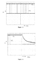
Fig. 3 is the graphical view of the status of the present invention at the normal voltage level. -
Fig. 4 is the graphical view of the reaction of the present invention to voltage irregularity. -
Fig. 5 is the graphical view of the application performed by changing the threshold voltage in the invention. - The descriptions of the abbreviations and references shown in the figures are illustrated in hereunder:
- Vcc: Data line (supply) voltage
- SCL: Serial clock line
- Q1: the first transistor
- Q2: the second transistor
- R1: the first resistor
- R2: the second resistor
- R3: the third resistor
- R4: the fourth resistor
- R5: the fifth resistor
- R6: the sixth resistor
- According to the present invention a circuit monitors the voltage of the 12C data line (Vcc) continuously, and in case of an error, the circuit grounds the serial clock line (SCL) of at least one electronic device accordingly. The principle of the said invention is illustrated in
Figure 1 . The voltage of data line is consistently monitored, and in case of a drop at the voltage of data line, serial clock line is grounded, and the monitoring process is carried on as long as there is no drop, and when the voltage of the data line returns to a determined level, the serial clock line is released, but in the event that it does not return, it is kept busy by being grounded. - The circuit diagram of the present system is illustrated as the example shown in
Figure 2 , where the first and second resistors (R1 and R2) determine a threshold voltage for enabling/disabling SCL connected to an electronic device, the third and the fifth resistors (R3 and R5) serve as a current limiter for the first and second transistors (Q1 and Q2), respectively, the value of first and second resistors are pre-determined in the site of manufacturer. The system is connected to data line supply voltage (Vcc) through theinput 1 and to the serial clock line (SCL) throughinput 2. - The graphic of the time-voltage amplitude of a data line which exchanges information and to which the present invention is connected under the normal operating conditions is illustrated in
Figure 3 . In the exemplary circuit made inFigure 2 for this example, the circuit elements have been selected as R1: 3900 ohm, R2: 910 ohm, R3: 1000 ohm, R4: 4700 ohm, R5: 1000 ohm, R6:12000 ohm, respectively and the transistors Q1 and Q2 as BC848B. - The base voltage of the first transistor (Q1) is 0.7 volts under the conditions observed in the graphic of the time-voltage amplitude shown in
Figure 3 , and this transistor (Q1) is on. Due to the voltage drop on the resistance (R4) created by the collector current of this transistor (Q1) when the first transistor (Q1) is on, the base voltage of the second transistor (Q2) is low, that is to say, Q2 is off. In such a case, the second transistor has no impact on the serial clock line (SCL). - When the data line voltage decreases below a predetermined level under the normal operating conditions, the base voltage of the first transistor (Q1) drops and turns off this transistor (Q1). The off state of the first transistor (Q1) turns on the second transistor (Q2) and grounds the serial clock line (SCL) and keeps it busy. As seen in
Figure 4 , when the system faces a voltage irregularity, it grounds the serial clock line. Since the data read/write operation to an electronic device(circuit element in this condition) is provided by SCL, data read/write is prevented when the serial clock line is grounded, no read/write operation can be performed on the band data line to which the system of the present invention is connected. - When the data line voltage (Vcc) rises to predetermined threshold level back, the first transistor (Q1) is turned on again, the second transistor (Q2) being off, and the serial clock line is resumed (grounding is over).
- The present invention can be used not only with the non-volatile memories such as EEPROM but also other circuit elements connected to the 12C line (e.g. video matrix switch, audio processor). The threshold voltage can be changed for the circuit elements by adjusting the first and the second resistor values (R1 and R2) in
Figure 2 . The threshold value can be either predetermined by the producer before or adjusted by the user. - For instance, R2 is selected as 910 ohm in the circuit used in the graphic shown in
Figure 4 . When the value of R2 is replaced by 1600 ohm, the level of the threshold voltage will be decreased, and the present invention will not keep busy the serial data line (SCL) until a certain drop at voltage value as it is shown in the graphic inFigure 5 .
Claims (13)
- A method for prevention of unwanted read/write operations which occur in circuit elements connected to a data line;
wherein the said method comprises the steps of:• determining a voltage threshold level for supply voltage on said data line• continuously measuring said supply voltage of said data line;• disabling read/write enable line of said circuit element when said data line supply voltage decreases below said threshold level. - A method according to claim 1, characterized in that, it enables said serial clock line of said circuit element when said data line supply voltage exceeds said threshold level.
- A system according to Claim 1, characterized in that said data line is 12C.
- A system according to Claim 1, characterized in that the said threshold level is determined in the site of manufacturer.
- A method according to Claim 1, characterized in that said circuit element connected to the said data line is a non-volatile memory.
- A method according to Claim 5, characterized in that the said non-volatile memory is an EEPROM.
- A method according to Claim 1, characterized in that said read/write enable line is serial clock line.
- A system for the prevention of unwanted read/write operations which might occur at circuit element connected to a data line comprises:• at least two resistors (R1, R2) to determine a threshold voltage level for said data line;• at least one transistor (Q1) for comparison of the predetermined threshold voltage value with the data line voltage (Vcc);• at least one transistor (Q2) which disables read/write operation of said circuit element by grounding serial clock line of said circuit element when said data line voltage level is below said threshold voltage level for said data line.
- A system according to Claim 8, characterized in that the said line providing read/write operations is the serial clock line (SCL).
- A system according to Claim 8, characterized in that the said threshold voltage level for said data line is a fixed value predetermined by producer.
- A system according to Claim 8, characterized in that said circuit element connected to the said data line is a non-volatile memory.
- A system according to Claim 12, characterized in that said non-volatile memory is an EEPROM.
- A system according to Claim 8, characterized in that said data line is an 12C data line.
Applications Claiming Priority (1)
| Application Number | Priority Date | Filing Date | Title |
|---|---|---|---|
| TR2007/01135A TR200701135A2 (en) | 2007-02-23 | 2007-02-23 | Prevention of unwanted I2C read / write operations |
Publications (2)
| Publication Number | Publication Date |
|---|---|
| EP1962291A1 true EP1962291A1 (en) | 2008-08-27 |
| EP1962291B1 EP1962291B1 (en) | 2011-04-13 |
Family
ID=39456580
Family Applications (1)
| Application Number | Title | Priority Date | Filing Date |
|---|---|---|---|
| EP08101745A Not-in-force EP1962291B1 (en) | 2007-02-23 | 2008-02-19 | Prevention of unwanted I2C read/write operations |
Country Status (4)
| Country | Link |
|---|---|
| EP (1) | EP1962291B1 (en) |
| AT (1) | ATE505792T1 (en) |
| DE (1) | DE602008006115D1 (en) |
| TR (1) | TR200701135A2 (en) |
Families Citing this family (1)
| Publication number | Priority date | Publication date | Assignee | Title |
|---|---|---|---|---|
| CN103345896B (en) * | 2013-06-14 | 2015-11-25 | 青岛海信电器股份有限公司 | Gamma correction buffer circuit, display device and anti-interference method |
Citations (3)
| Publication number | Priority date | Publication date | Assignee | Title |
|---|---|---|---|---|
| EP0155113A2 (en) * | 1984-02-28 | 1985-09-18 | Fujitsu Limited | Voltage level detection circuit |
| US4580039A (en) | 1982-01-28 | 1986-04-01 | Kienzle Apparate Gmbh | Circuit arrangement for the protection of data in volatile write-read memories (RAM) |
| US6198661B1 (en) | 1998-11-26 | 2001-03-06 | Hyundai Electronics Industries Co., Ltd. | Sensing circuit for semiconductor device and sensing method using the same |
-
2007
- 2007-02-23 TR TR2007/01135A patent/TR200701135A2/en unknown
-
2008
- 2008-02-19 EP EP08101745A patent/EP1962291B1/en not_active Not-in-force
- 2008-02-19 AT AT08101745T patent/ATE505792T1/en not_active IP Right Cessation
- 2008-02-19 DE DE602008006115T patent/DE602008006115D1/en active Active
Patent Citations (3)
| Publication number | Priority date | Publication date | Assignee | Title |
|---|---|---|---|---|
| US4580039A (en) | 1982-01-28 | 1986-04-01 | Kienzle Apparate Gmbh | Circuit arrangement for the protection of data in volatile write-read memories (RAM) |
| EP0155113A2 (en) * | 1984-02-28 | 1985-09-18 | Fujitsu Limited | Voltage level detection circuit |
| US6198661B1 (en) | 1998-11-26 | 2001-03-06 | Hyundai Electronics Industries Co., Ltd. | Sensing circuit for semiconductor device and sensing method using the same |
Also Published As
| Publication number | Publication date |
|---|---|
| TR200701135A2 (en) | 2008-09-22 |
| DE602008006115D1 (en) | 2011-05-26 |
| EP1962291B1 (en) | 2011-04-13 |
| ATE505792T1 (en) | 2011-04-15 |
Similar Documents
| Publication | Publication Date | Title |
|---|---|---|
| US9523722B2 (en) | Method and apparatus for supply voltage glitch detection in a monolithic integrated circuit device | |
| US8321727B2 (en) | System and method responsive to a rate of change of a performance parameter of a memory | |
| EP1551031B1 (en) | Semiconductor device card | |
| EP2982997B1 (en) | Method and apparatus for supply voltage glitch detection in a monolithic integrated circuit device | |
| US10474214B2 (en) | Data storage device and method for monitoring power storage capability of secondary power of data storage device | |
| WO2006036443A3 (en) | Method and apparatus for protecting an integrated circuit from erroneous operation | |
| US20090144834A1 (en) | Data processing circuit and communication mobile terminal device | |
| US10275017B2 (en) | Power circuit and memory device using the same | |
| CN107393597B (en) | For detecting the overvoltage detection circuit of the overvoltage spike from external power supply | |
| CN113138938A (en) | Memory protection device and method and electronic equipment | |
| EP1962291B1 (en) | Prevention of unwanted I2C read/write operations | |
| CN105629028B (en) | Detect supply voltage surging method and circuit of single-chip integrated device | |
| KR101551817B1 (en) | Memory erase method and apparatus for the same | |
| US5941987A (en) | Reference cell for integrated circuit security | |
| US5831347A (en) | Apparatus for determining if the duration of a power failure exceeded predetermined limits | |
| JP4188563B2 (en) | Method and apparatus for high-speed manufacturing programming and low-voltage in-system writing for programmable logic devices | |
| US10978162B2 (en) | Method and semiconductor device for protecting a semiconductor integrated circuit from reverse engineering | |
| US5586077A (en) | Circuit device and corresponding method for resetting non-volatile and electrically programmable memory devices | |
| US20100127767A1 (en) | Integrated Circuit Device Including Noise Filter | |
| CN110417389B (en) | Power-on reset circuit | |
| US9437237B1 (en) | Method to detect power loss through data storage device spindle speed | |
| US6154067A (en) | Methods of and apparatus for monitoring the termination status of a SCSI bus | |
| JPH11327665A (en) | Power supply voltage monitoring circuit | |
| US20110153961A1 (en) | Storage device with function of voltage abnormal protection and operation method thereof | |
| KR101730638B1 (en) | Method and apparatus for supply voltage glitch detection in a monolithic integrated circuit device |
Legal Events
| Date | Code | Title | Description |
|---|---|---|---|
| PUAI | Public reference made under article 153(3) epc to a published international application that has entered the european phase |
Free format text: ORIGINAL CODE: 0009012 |
|
| 17P | Request for examination filed |
Effective date: 20080314 |
|
| AK | Designated contracting states |
Kind code of ref document: A1 Designated state(s): AT BE BG CH CY CZ DE DK EE ES FI FR GB GR HR HU IE IS IT LI LT LU LV MC MT NL NO PL PT RO SE SI SK TR |
|
| AX | Request for extension of the european patent |
Extension state: AL BA MK RS |
|
| 17Q | First examination report despatched |
Effective date: 20090319 |
|
| AKX | Designation fees paid |
Designated state(s): AT BE BG CH CY CZ DE DK EE ES FI FR GB GR HR HU IE IS IT LI LT LU LV MC MT NL NO PL PT RO SE SI SK TR |
|
| GRAP | Despatch of communication of intention to grant a patent |
Free format text: ORIGINAL CODE: EPIDOSNIGR1 |
|
| GRAS | Grant fee paid |
Free format text: ORIGINAL CODE: EPIDOSNIGR3 |
|
| GRAA | (expected) grant |
Free format text: ORIGINAL CODE: 0009210 |
|
| AK | Designated contracting states |
Kind code of ref document: B1 Designated state(s): AT BE BG CH CY CZ DE DK EE ES FI FR GB GR HR HU IE IS IT LI LT LU LV MC MT NL NO PL PT RO SE SI SK TR |
|
| REG | Reference to a national code |
Ref country code: GB Ref legal event code: FG4D |
|
| REG | Reference to a national code |
Ref country code: CH Ref legal event code: EP |
|
| REG | Reference to a national code |
Ref country code: IE Ref legal event code: FG4D |
|
| REF | Corresponds to: |
Ref document number: 602008006115 Country of ref document: DE Date of ref document: 20110526 Kind code of ref document: P |
|
| REG | Reference to a national code |
Ref country code: DE Ref legal event code: R096 Ref document number: 602008006115 Country of ref document: DE Effective date: 20110526 |
|
| REG | Reference to a national code |
Ref country code: NL Ref legal event code: VDEP Effective date: 20110413 |
|
| LTIE | Lt: invalidation of european patent or patent extension |
Effective date: 20110413 |
|
| PG25 | Lapsed in a contracting state [announced via postgrant information from national office to epo] |
Ref country code: PT Free format text: LAPSE BECAUSE OF FAILURE TO SUBMIT A TRANSLATION OF THE DESCRIPTION OR TO PAY THE FEE WITHIN THE PRESCRIBED TIME-LIMIT Effective date: 20110816 Ref country code: SE Free format text: LAPSE BECAUSE OF FAILURE TO SUBMIT A TRANSLATION OF THE DESCRIPTION OR TO PAY THE FEE WITHIN THE PRESCRIBED TIME-LIMIT Effective date: 20110413 Ref country code: HR Free format text: LAPSE BECAUSE OF FAILURE TO SUBMIT A TRANSLATION OF THE DESCRIPTION OR TO PAY THE FEE WITHIN THE PRESCRIBED TIME-LIMIT Effective date: 20110413 Ref country code: NO Free format text: LAPSE BECAUSE OF FAILURE TO SUBMIT A TRANSLATION OF THE DESCRIPTION OR TO PAY THE FEE WITHIN THE PRESCRIBED TIME-LIMIT Effective date: 20110713 Ref country code: LT Free format text: LAPSE BECAUSE OF FAILURE TO SUBMIT A TRANSLATION OF THE DESCRIPTION OR TO PAY THE FEE WITHIN THE PRESCRIBED TIME-LIMIT Effective date: 20110413 |
|
| PG25 | Lapsed in a contracting state [announced via postgrant information from national office to epo] |
Ref country code: BE Free format text: LAPSE BECAUSE OF FAILURE TO SUBMIT A TRANSLATION OF THE DESCRIPTION OR TO PAY THE FEE WITHIN THE PRESCRIBED TIME-LIMIT Effective date: 20110413 Ref country code: AT Free format text: LAPSE BECAUSE OF FAILURE TO SUBMIT A TRANSLATION OF THE DESCRIPTION OR TO PAY THE FEE WITHIN THE PRESCRIBED TIME-LIMIT Effective date: 20110413 Ref country code: CY Free format text: LAPSE BECAUSE OF FAILURE TO SUBMIT A TRANSLATION OF THE DESCRIPTION OR TO PAY THE FEE WITHIN THE PRESCRIBED TIME-LIMIT Effective date: 20110413 Ref country code: FI Free format text: LAPSE BECAUSE OF FAILURE TO SUBMIT A TRANSLATION OF THE DESCRIPTION OR TO PAY THE FEE WITHIN THE PRESCRIBED TIME-LIMIT Effective date: 20110413 Ref country code: IS Free format text: LAPSE BECAUSE OF FAILURE TO SUBMIT A TRANSLATION OF THE DESCRIPTION OR TO PAY THE FEE WITHIN THE PRESCRIBED TIME-LIMIT Effective date: 20110813 Ref country code: ES Free format text: LAPSE BECAUSE OF FAILURE TO SUBMIT A TRANSLATION OF THE DESCRIPTION OR TO PAY THE FEE WITHIN THE PRESCRIBED TIME-LIMIT Effective date: 20110724 Ref country code: SI Free format text: LAPSE BECAUSE OF FAILURE TO SUBMIT A TRANSLATION OF THE DESCRIPTION OR TO PAY THE FEE WITHIN THE PRESCRIBED TIME-LIMIT Effective date: 20110413 Ref country code: GR Free format text: LAPSE BECAUSE OF FAILURE TO SUBMIT A TRANSLATION OF THE DESCRIPTION OR TO PAY THE FEE WITHIN THE PRESCRIBED TIME-LIMIT Effective date: 20110714 Ref country code: LV Free format text: LAPSE BECAUSE OF FAILURE TO SUBMIT A TRANSLATION OF THE DESCRIPTION OR TO PAY THE FEE WITHIN THE PRESCRIBED TIME-LIMIT Effective date: 20110413 |
|
| PG25 | Lapsed in a contracting state [announced via postgrant information from national office to epo] |
Ref country code: NL Free format text: LAPSE BECAUSE OF FAILURE TO SUBMIT A TRANSLATION OF THE DESCRIPTION OR TO PAY THE FEE WITHIN THE PRESCRIBED TIME-LIMIT Effective date: 20110413 |
|
| PG25 | Lapsed in a contracting state [announced via postgrant information from national office to epo] |
Ref country code: EE Free format text: LAPSE BECAUSE OF FAILURE TO SUBMIT A TRANSLATION OF THE DESCRIPTION OR TO PAY THE FEE WITHIN THE PRESCRIBED TIME-LIMIT Effective date: 20110413 Ref country code: CZ Free format text: LAPSE BECAUSE OF FAILURE TO SUBMIT A TRANSLATION OF THE DESCRIPTION OR TO PAY THE FEE WITHIN THE PRESCRIBED TIME-LIMIT Effective date: 20110413 |
|
| PLBE | No opposition filed within time limit |
Free format text: ORIGINAL CODE: 0009261 |
|
| STAA | Information on the status of an ep patent application or granted ep patent |
Free format text: STATUS: NO OPPOSITION FILED WITHIN TIME LIMIT |
|
| PG25 | Lapsed in a contracting state [announced via postgrant information from national office to epo] |
Ref country code: SK Free format text: LAPSE BECAUSE OF FAILURE TO SUBMIT A TRANSLATION OF THE DESCRIPTION OR TO PAY THE FEE WITHIN THE PRESCRIBED TIME-LIMIT Effective date: 20110413 Ref country code: RO Free format text: LAPSE BECAUSE OF FAILURE TO SUBMIT A TRANSLATION OF THE DESCRIPTION OR TO PAY THE FEE WITHIN THE PRESCRIBED TIME-LIMIT Effective date: 20110413 Ref country code: PL Free format text: LAPSE BECAUSE OF FAILURE TO SUBMIT A TRANSLATION OF THE DESCRIPTION OR TO PAY THE FEE WITHIN THE PRESCRIBED TIME-LIMIT Effective date: 20110413 Ref country code: DK Free format text: LAPSE BECAUSE OF FAILURE TO SUBMIT A TRANSLATION OF THE DESCRIPTION OR TO PAY THE FEE WITHIN THE PRESCRIBED TIME-LIMIT Effective date: 20110413 |
|
| 26N | No opposition filed |
Effective date: 20120116 |
|
| REG | Reference to a national code |
Ref country code: DE Ref legal event code: R097 Ref document number: 602008006115 Country of ref document: DE Effective date: 20120116 |
|
| PG25 | Lapsed in a contracting state [announced via postgrant information from national office to epo] |
Ref country code: MC Free format text: LAPSE BECAUSE OF NON-PAYMENT OF DUE FEES Effective date: 20120229 |
|
| REG | Reference to a national code |
Ref country code: CH Ref legal event code: PL |
|
| PG25 | Lapsed in a contracting state [announced via postgrant information from national office to epo] |
Ref country code: LI Free format text: LAPSE BECAUSE OF NON-PAYMENT OF DUE FEES Effective date: 20120229 Ref country code: CH Free format text: LAPSE BECAUSE OF NON-PAYMENT OF DUE FEES Effective date: 20120229 |
|
| REG | Reference to a national code |
Ref country code: IE Ref legal event code: MM4A |
|
| PG25 | Lapsed in a contracting state [announced via postgrant information from national office to epo] |
Ref country code: IE Free format text: LAPSE BECAUSE OF NON-PAYMENT OF DUE FEES Effective date: 20120219 |
|
| PG25 | Lapsed in a contracting state [announced via postgrant information from national office to epo] |
Ref country code: BG Free format text: LAPSE BECAUSE OF FAILURE TO SUBMIT A TRANSLATION OF THE DESCRIPTION OR TO PAY THE FEE WITHIN THE PRESCRIBED TIME-LIMIT Effective date: 20110713 |
|
| PG25 | Lapsed in a contracting state [announced via postgrant information from national office to epo] |
Ref country code: MT Free format text: LAPSE BECAUSE OF FAILURE TO SUBMIT A TRANSLATION OF THE DESCRIPTION OR TO PAY THE FEE WITHIN THE PRESCRIBED TIME-LIMIT Effective date: 20110413 |
|
| PG25 | Lapsed in a contracting state [announced via postgrant information from national office to epo] |
Ref country code: LU Free format text: LAPSE BECAUSE OF NON-PAYMENT OF DUE FEES Effective date: 20120219 |
|
| PG25 | Lapsed in a contracting state [announced via postgrant information from national office to epo] |
Ref country code: HU Free format text: LAPSE BECAUSE OF FAILURE TO SUBMIT A TRANSLATION OF THE DESCRIPTION OR TO PAY THE FEE WITHIN THE PRESCRIBED TIME-LIMIT Effective date: 20080219 |
|
| REG | Reference to a national code |
Ref country code: FR Ref legal event code: PLFP Year of fee payment: 9 |
|
| REG | Reference to a national code |
Ref country code: FR Ref legal event code: PLFP Year of fee payment: 10 |
|
| REG | Reference to a national code |
Ref country code: FR Ref legal event code: PLFP Year of fee payment: 11 |
|
| PGFP | Annual fee paid to national office [announced via postgrant information from national office to epo] |
Ref country code: IT Payment date: 20210222 Year of fee payment: 14 Ref country code: FR Payment date: 20210224 Year of fee payment: 14 |
|
| PGFP | Annual fee paid to national office [announced via postgrant information from national office to epo] |
Ref country code: GB Payment date: 20210219 Year of fee payment: 14 Ref country code: DE Payment date: 20210217 Year of fee payment: 14 |
|
| PGFP | Annual fee paid to national office [announced via postgrant information from national office to epo] |
Ref country code: TR Payment date: 20220216 Year of fee payment: 15 |
|
| REG | Reference to a national code |
Ref country code: DE Ref legal event code: R119 Ref document number: 602008006115 Country of ref document: DE |
|
| GBPC | Gb: european patent ceased through non-payment of renewal fee |
Effective date: 20220219 |
|
| PG25 | Lapsed in a contracting state [announced via postgrant information from national office to epo] |
Ref country code: FR Free format text: LAPSE BECAUSE OF NON-PAYMENT OF DUE FEES Effective date: 20220228 |
|
| PG25 | Lapsed in a contracting state [announced via postgrant information from national office to epo] |
Ref country code: GB Free format text: LAPSE BECAUSE OF NON-PAYMENT OF DUE FEES Effective date: 20220219 Ref country code: DE Free format text: LAPSE BECAUSE OF NON-PAYMENT OF DUE FEES Effective date: 20220901 |
|
| PG25 | Lapsed in a contracting state [announced via postgrant information from national office to epo] |
Ref country code: IT Free format text: LAPSE BECAUSE OF NON-PAYMENT OF DUE FEES Effective date: 20220219 |
|
| PG25 | Lapsed in a contracting state [announced via postgrant information from national office to epo] |
Ref country code: TR Free format text: LAPSE BECAUSE OF NON-PAYMENT OF DUE FEES Effective date: 20230219 |