EP1551031B1 - Semiconductor device card - Google Patents
Semiconductor device card Download PDFInfo
- Publication number
- EP1551031B1 EP1551031B1 EP04030397.6A EP04030397A EP1551031B1 EP 1551031 B1 EP1551031 B1 EP 1551031B1 EP 04030397 A EP04030397 A EP 04030397A EP 1551031 B1 EP1551031 B1 EP 1551031B1
- Authority
- EP
- European Patent Office
- Prior art keywords
- voltage
- host
- working voltage
- semiconductor device
- working
- Prior art date
- Legal status (The legal status is an assumption and is not a legal conclusion. Google has not performed a legal analysis and makes no representation as to the accuracy of the status listed.)
- Active
Links
- 239000004065 semiconductor Substances 0.000 title claims description 42
- 239000002184 metal Substances 0.000 claims description 16
- 230000005540 biological transmission Effects 0.000 claims description 4
- 230000008878 coupling Effects 0.000 claims description 4
- 238000010168 coupling process Methods 0.000 claims description 4
- 238000005859 coupling reaction Methods 0.000 claims description 4
- 238000007599 discharging Methods 0.000 claims description 3
- 239000003990 capacitor Substances 0.000 claims description 2
- 101100191136 Arabidopsis thaliana PCMP-A2 gene Proteins 0.000 description 12
- 101100048260 Saccharomyces cerevisiae (strain ATCC 204508 / S288c) UBX2 gene Proteins 0.000 description 12
- 101100422768 Saccharomyces cerevisiae (strain ATCC 204508 / S288c) SUL2 gene Proteins 0.000 description 9
- 238000010586 diagram Methods 0.000 description 4
- 238000001514 detection method Methods 0.000 description 3
- 230000008901 benefit Effects 0.000 description 2
- 238000006243 chemical reaction Methods 0.000 description 2
- 230000006870 function Effects 0.000 description 2
- 238000004519 manufacturing process Methods 0.000 description 2
- 230000007246 mechanism Effects 0.000 description 2
- 230000004044 response Effects 0.000 description 2
- 230000003247 decreasing effect Effects 0.000 description 1
- 238000005516 engineering process Methods 0.000 description 1
Images


Classifications
-
- G—PHYSICS
- G06—COMPUTING; CALCULATING OR COUNTING
- G06F—ELECTRIC DIGITAL DATA PROCESSING
- G06F12/00—Accessing, addressing or allocating within memory systems or architectures
-
- G—PHYSICS
- G11—INFORMATION STORAGE
- G11C—STATIC STORES
- G11C5/00—Details of stores covered by group G11C11/00
- G11C5/14—Power supply arrangements, e.g. power down, chip selection or deselection, layout of wirings or power grids, or multiple supply levels
- G11C5/147—Voltage reference generators, voltage or current regulators; Internally lowered supply levels; Compensation for voltage drops
-
- G—PHYSICS
- G11—INFORMATION STORAGE
- G11C—STATIC STORES
- G11C16/00—Erasable programmable read-only memories
- G11C16/02—Erasable programmable read-only memories electrically programmable
- G11C16/06—Auxiliary circuits, e.g. for writing into memory
- G11C16/30—Power supply circuits
Definitions
- the invention relates to a semiconductor device card such as a memory card.
- a semiconductor device card such as a memory card.
- the invention is described herein for a memory card as an ex ample. However, the invention may in general be used for any type of semiconductor device card.
- Fig. 1 shows a memory card 102 of the prior art for transmission of data between a memory device 104 and a host 106.
- the memory card 102 is inserted into the host 106 that provides a host voltage to the memory card 102.
- the host voltage from the host 106 is coupled to a memory controller 108 and the memory device 104. In such a manner, such components 104 and 108 of the memory card 102 derive power from the host 106 for operation.
- the memory device 104 operates properly when the working voltage of the memory device 104 is substantially same as the host voltage from the host 106.
- the host 106 and the memory device 104 both operate with a working voltage of 3.3 Volts.
- the prior art memory card 102 cannot be used with a host providing a different host voltage from the working voltage of the memory device 104.
- the host 106 operates properly with the memory card 102 when the memory device 104 has a substantially same working voltage as the host voltage.
- the memory device 104 operates properly when interfaced to the host 106 providing substantially the same host voltage as the working voltage of the memory device 104.
- U.S. Patent No. 5,828,892 to Mizuta discloses a memory card 11 having a power source voltage control circuit 12 that provides a desired working voltage to an I/O (input/output buffer) 13 and a DRAM (dynamic random access memory) device 14, as illustrated in Fig. 2 .
- the voltage control circuit 12 provides the desired working voltage (such as 3.3 Volts for example) even when the host voltage Vcc is higher (such as 5.0 Volts for example).
- Fig. 3 shows the implementation of the voltage control circuit 12 as disclosed in Mizuta.
- the host voltage is received at an input 28 that is coupled to a first window comparator 21 and a second window comparator 24.
- the first window comparator 21 turns on a first MOSFET 22 if the host voltage is within a first range of values such as 4.5 Volts to 5.5 Volts.
- the second window comparator 24 turns on a second MOSFET 25 if the host voltage is within a second range of values such as 3.0 Volts to 3.6 Volts.
- the first MOSFET 22 that is turned on couples the host voltage to a DC-DC converter 23 that converts the host voltage in the first range of values down to the working voltage of the DRAM 14 (such as 3.3 Volts for example). Such as stepped down working voltage is generated on an output terminal 29.
- the second MOSFET 25 that is turned on simply couples the host voltage in the second range of values to the output terminal 29 as the working voltage of the DRAM 14.
- the voltage control circuit 12 provides the working voltage that is lower than or equal to the host voltage. Consequently, the memory card 12 may be used with different types of hosts providing host voltages that are greater than or equal to the working voltage of the DRAM 14.
- the memory card 11 of Mizuta accommodates different host voltages to operate with different types of hosts. However, the memory card 11 of Mizuta accommodates a predetermined working voltage of the memory device 14 as the DC-DC converter 23 is fixed for conversion to the predetermined working voltage. With advancement of technology, the working voltage of the memory device 14 may be decreased further and further. Thus, the memory device within a memory card may have one of various working voltages. However, the memory card 11 of Mizuta does not accommodate various working voltages of the memory device 14.
- Patent publication US 5,329,491 against which the preamble is based on discloses a flash memory card capable of automatically configuring itself to an externally supplied card power voltage.
- the card comprises a voltage detection circuit to detect the actual value of the external power supply voltage and a card control logic receiving the detection signal of the voltage detection circuit and in response thereof configures a memory array of the card to work with said actual external supply voltage.
- a voltage conversion circuit provides appropriate device power, program, and erase power supply voltages using the input external supply voltage.
- Patent publication US 5,773,901 discloses a card-receiving host capable of working with different types of cards such as high or low voltage cards and high or low current cards to be selectively inserted into a card-receiving slot.
- the host is provided with voltage and current sensing switches operated by a corresponding voltage or current discrimination key provided at the card of corresponding type so as to detect the type of card when it is inserted into the slot.
- the host further comprises means for selectively providing an appropriate operating voltage and/or current to the card in response to the detected card type.
- the invention solves this problem by providing a semiconductor device card having the device features of claim 1.
- Advantageous embodiments of the invention are mentioned in the subclaims, the wording of which is herewith fully incorporated into the description by reference to avoid unnecessary text repetitions.
- the semiconductor device is a memory device for the semiconductor device card that is a memory card.
- the semiconductor device card includes a memory controller having the working voltage generator.
- the memory controller includes a data processing device, a host interface, and a memory interface.
- the data processing device controls data transmission between a host and the memory device.
- the host interface interfaces the data processing device to the host, and the memory interface interfaces the data processing device to the memory device.
- a host voltage is applied to the host interface, the data processing device, and the memory interface.
- the working voltage is applied to the memory interface and the memory device.
- the working voltage generator generates the working voltage from the host voltage.
- the working voltage generator includes a feed-back path for maintaining the working voltage substantially at the desired level.
- the feed-back path includes an output node with the working voltage generated thereon.
- a switch is coupled between the host voltage and the output node.
- a comparator compares the working voltage and the desired level to turn on the switch for charging/discharging the output node when the working voltage is not equal to the desired level.
- a reference voltage generator generates a target voltage having the desired level and being coupled to the comparator.
- the working voltage indicator further includes at least one fuse circuit coupled to the multiplexer, and a respective logical state of each output of the fuse circuit is set to indicate the selected target voltage.
- the working voltage indicator includes a voltage select decoder that asserts one of a voltage up signal, a voltage down signal, and a voltage pass signal from comparing the host voltage and the working voltage.
- a first voltage generator generates the working voltage boosted from the host voltage when the voltage up signal is asserted to indicate that the desired level of the working voltage is greater than the host voltage.
- a second voltage generator generates the working voltage as the host voltage when the voltage pass signal is asserted to indicate that the desired level of the working voltage is substantially equal to the host voltage.
- a third voltage generator generates the working voltage stepped down from the host voltage when the voltage down signal is asserted to indicate that the desired level of the working voltage is less than the host voltage.
- the working voltage indicator includes a variable resistance block coupled to the output node and having a plurality of metal lines with variable coupling for adjusting the working voltage at the output node.
- the working voltage generator generates the working voltage having the desired level that is any of higher than, lower than, or substantially equal to the host voltage.
- the semiconductor device card is easily adaptable to accommodate various working voltages of the semiconductor device.
- the invention is described in the following for a memory card. However, the invention may in general be used for any type of semiconductor device card.
- a semiconductor card 202 of an embodiment of the invention transmits data between a semiconductor device 204 and a host 206.
- the semiconductor device 204 is a non-volatile memory device such as a flash memory device, an EEPROM (electrically erasable programmable read only memory), a PRAM (phase-change random access memory), a MRAM (magnetic random access memory), or a FRAM (ferro-electric random access memory), in one embodiment of the invention.
- the memory card 202 is referred to as a "flash card”.
- flash cards are of many types such as MMC (multi-media card), SD (security device), CF (contact flash), or memory sticks depending on the manufacturer or the application.
- the host 206 that uses the memory card 202 to particular advantage may be common portable devices such as MP3 players, camcorders, digital cameras, PDAs (personal digital assistants), and mobile products.
- the invention may be practiced when the semiconductor card 202 is for any type of semiconductor device 204 and any type of host 206.
- the memory card 202 includes a memory controller 208 with a voltage regulator 210, a host I/F (interface) 212, a data processing device 214, and a memory I/F (interface) 216.
- the host I/F 212 interfaces the memory controller 208 to the host 206
- the memory I/F 216 interfaces the memory controller 208 to the memory device 204.
- the data processing device 214 controls operation of the interfaces 212 and 216 for data transmission between the memory device 204 and the host 206.
- the voltage regulator 210 receives the host voltage from the host 206 and generates a working voltage coupled to the memory device 204 and the memory I/F 216, in an embodiment of the invention.
- the host voltage is coupled to the host I/F 212, the data processing device 214, and the memory I/F 216, in an embodiment of the invention.
- the voltage regulator 210 is a working voltage generator in one embodiment of the invention.
- the voltage regulator 210 includes a reference voltage generator 220 that generates a target voltage coupled to a negative input of a comparator 222.
- the output of the comparator 222 is coupled to the gate of a PMOSFET 224 having a source coupled to the host voltage from the host 206.
- the drain of the PMOSFET 224 is coupled to the positive input of the comparator 222 via a feed-back path 226.
- the drain of the PMOSFET 224 forms an output node 228 having the working voltage generated thereon.
- a decoupling capacitor 230 is coupled between the output node 228 and a low voltage source VSS which is a ground node of the host 206 in one embodiment of the invention.
- the reference voltage generator 220 During operation of the voltage regulator of Fig. 5 , the reference voltage generator 220 generates a target voltage that has the desired level (such as 1.8 Volts for example) of the working voltage to be generated at the output node 228. The level of the working voltage generated at the output node 228 is compared to the target voltage from the reference voltage generator 220.
- the desired level such as 1.8 Volts for example
- the PMOSFET 224 Upon power-up, if the level of the working voltage is less than the target voltage, the PMOSFET 224 is turned on by the negative output of the comparator 222 to charge up the output node 228 for increasing the working voltage. When the working voltage at the output node 228 reaches the target voltage, the positive output of the comparator 222 turns off the PMOSFET 224.
- the feed-back path 226 maintains the working voltage at the output node 228 to be substantially equal to the target voltage from the reference voltage generator 220.
- the working voltage supplied to the memory device 204 has the desired level for any host voltage (such as 3.3 Volts in Fig. 5 for example) greater than the desired level of the working voltage.
- Fig. 6 shows an alternative embodiment of the voltage regulator 210 including a working voltage indicator 240 and a working voltage generator 242.
- the working voltage indicator 240 includes a first reference voltage generator 244 for generating a first target voltage with a first level (2.7 Volts for example).
- the working voltage indicator 240 includes a second reference voltage generator 246 for generating a second target voltage with a second level (1.8 Volts for example).
- the working voltage indicator 240 further includes a multiplexer 248 that inputs the target voltages from the first and second reference voltage generators 244 and 246.
- a select signal SEL is input to the multiplexer that selects one of the target voltages from the first and second reference voltage generators 244 and 246 as a selected target voltage coupled to the negative input of the comparator 222.
- the working voltage generator 242 of Fig. 6 operates similarly with that of Fig. 5 to generate the working voltage at the output node 228 having the desired level of the selected target voltage from the multiplexer 248.
- the working voltage indicator 240 of Fig. 6 allows for flexibility in the working voltage of the memory device 204. With such a working voltage indicator 240, the desired level of the working voltage used by the memory device 204 may vary between the two target voltages from the reference voltage generators 244 and 246.
- FIG. 7 shows another embodiment of the voltage regulator 210 having the working voltage generator 242 similar to that in Fig. 6 .
- a working voltage indicator 250 of Fig. 7 includes first, second, third, and fourth reference voltage generators 252, 254, 256, and 258, respectively.
- Each of the reference voltage generators 252, 254, 256, and 258 generates a respective target voltage, such as 5.0 Volts, 3.3 Volts, 2.7 Volts, and 1.8 Volts, respectively, for example.
- Such target voltages from the reference voltage generators 252, 254, 256, and 258 are input by a multiplexer 260 that selects one of such target voltages as a selected target voltage coupled to the negative input of the comparator 222.
- the multiplexer 260 selects one of the target voltages from the reference voltage generators 252, 254, 256, and 258 depending on the respective logical state of each of two select signals SEL1 and SEL2.
- the working voltage generator 242 of Fig. 7 operates similarly with that of Fig. 6 to generate the working voltage at the output node 228 having the desired level of the selected target voltage from the multiplexer 260.
- the working voltage indicator 250 of Fig. 7 allows for flexibility in the working voltage of the memory device 204.
- the desired level of the working voltage used by the memory device 204 may vary between the four target voltages from the reference voltage generators 252, 254, 256, and 258.
- Fig. 8 illustrates an example mechanism for setting the respective logical state of each of the select signals SEL1 and SEL2 in Fig. 7 .
- the memory card 202 includes a first IC (integrated circuit) package of the memory controller 208 and includes a second IC package of the memory device 204.
- the memory card 202 includes a plurality of contact pads such as a first contact pad 262 coupled to the host voltage VDD and a second contact pad 264 coupled to the host ground VSS.
- a host voltage line 266 coupled to the first contact pad 262 and a host ground line 268 coupled to the second contact pad 264 are formed around the memory controller 208.
- a first pin 272 of the memory controller 208 has the first select signal SEL1 applied thereon and is coupled to one of the host voltage line 266 and the host ground line 268. If the first pin 272 is coupled to the host voltage line 266, the first select signal SEL1 has a logical high state. If the first pin 272 is coupled to the host ground line 268, the first select signal SEL1 has a logical low state.
- a second pin 274 of the memory controller 208 has the second select signal SEL2 applied thereon and is coupled to one of the host voltage line 266 and the host ground line 268. If the second pin 274 is coupled to the host voltage line 266, the second select signal SEL2 has a logical high state. If the second pin 274 is coupled to the host ground line 268, the second select signal SEL2 has a logical low state.
- the first and second pins 272 and 274 are each coupled to one of the lines 266 and 268 such that the multiplexer 260 selects one of the four target voltages from the reference voltage generators 252, 254, 256, and 258 corresponding to the desired level of the working voltage of the memory device 204.
- the first and second pins 272 and 274 are set with a respective logical state as part of the working voltage indicator 250 for indicating the desired level of the working voltage of the memory device 204.
- the working voltage generated on the output node 228 is applied on a third pin 276 of the memory controller 208 that is coupled to a working voltage pin 278 of the memory device 204.
- a ground pin 280 of the memory device 204 is coupled to the host ground line 268 such that the working voltage on the working voltage pin 278 is with respect to the host ground VSS, in one embodiment of the invention.
- just one pin such as the first pin 272 of the memory controller 208 may be used for having the select signal SEL of the multiplexer 248 applied thereon.
- the first pin 272 is coupled to one of the lines 266 and 268 for setting the logical state of the select signal SEL in Fig. 6 .
- Fig. 9 shows another mechanism for setting the respective logical state of each of the select signals SEL1 and SEL2 in Fig. 7 .
- Fig. 9 shows a first fuse circuit 282 and a second fuse circuit 287 coupled to a power-up initialization signal generator 285 coupled between the host voltage VDD and the host ground VSS. Upon power up, the initialization signal generator 285 generates a biasing voltage VCCH with a logical high state.
- the first fuse circuit 282 includes a fuse 284 coupled to a drain of a PMOSFET 286 at a first node 288.
- the PMOSFET 228 has a source coupled to the host voltage VDD and a gate having the VCCH bias applied thereon.
- An NMOSFET 290 has a drain coupled to a second node 292 of the fuse 284, a source coupled to the host ground node VSS, and a gate having the VCCH bias applied thereon.
- the first fuse circuit 282 also includes a latch 294 of a loop of inverters 296 and 298 coupled to the first node 288 of the fuse 284.
- the output of the latch 294 generates the first select signal SEL1.
- the SEL1 signal is a logical low state.
- the SEL1 signal is a logical high state.
- the fuse 284 of the first fuse circuit 282 is cut or left not cut for setting the logical state of the SEL1 signal.
- the second fuse circuit 287 is similar to the first fuse circuit 282 with another fuse within the second fuse circuit 287 that is cut or left not cut for setting the logical state of the SEL2 signal.
- the respective fuse within each of the first and second fuse circuits 282 and 287 is cut or left not cut such that the multiplexer 260 selects one of the four target voltages from the reference voltage generators 252, 254, 256, and 258 corresponding to the desired level of the working voltage of the memory device 204.
- the respective fuse within each of the first and second fuse circuits 282 and 287 is set as part of the working voltage indicator 250 for indicating the desired level of the working voltage of the memory device 204.
- Fig. 10 shows an alternative embodiment of the voltage regulator 210 with a working voltage generated at the output node 228.
- the level of such a working voltage is adjustable with variable coupling of a plurality of metal lines 302, 304, and 306 within a variable resistance block 320.
- Elements having the same reference number in Figs. 5 and 10 refer to elements having similar structure and function.
- a plurality of resistors are coupled from the drain of the PMOSFET 224.
- a first resistor 308 is coupled between the drain of the PMOSFET 224 and a feed-back path node 310.
- a second resistor 310 is coupled between the feed-back path node 310 and a first metal line 302.
- a third resistor 314 is coupled between the first metal line 302 and a second metal line 304.
- a fourth resistor 316 is coupled between the second metal line 304 and a third metal line 306 which is also coupled to the host ground node VSS.
- any of the metal lines 302, 304, and 306 may be coupled together to vary the resistance of the variable resistance block 320. For example, if the first metal line 302 is connected to the third metal line 306, the resistance through the resistance block 320 is zero. If the second metal line 304 is connected to the third metal line 306, the resistance through the resistance block 320 is the resistance of the third resistor 314. If the first metal line 302 is connected to the second metal line 304, the resistance through the resistance block 320 is the resistance of the fourth resistor 316.
- a voltage substantially similar to the reference voltage generated by the reference voltage generator 220 is generated at the feed-back path node 310.
- a variable level of current flows through the resistors 308, 312, 314, and 316.
- the working voltage generated at the output node 228 may be varied.
- the connection of the metal lines 302, 304, and 306 is varied for adjusting the level of the working voltage generated at the output node 228.
- the voltage regulator 210 of Fig. 10 allows for flexibility in the working voltage of the memory device 204.
- Fig. 11 shows an alternative embodiment of the voltage regulator 210 having a working voltage indicator 330 and a working voltage generator 332.
- the working voltage indicator includes a host voltage level detector 334 and a working voltage decoder 336.
- the host voltage level detector 334 indicates the level of the host voltage VDD to the working voltage decoder 336.
- the working voltage decoder 336 inputs first and second select signals SEL1 and SEL2 each having a respective logical state for indicating a desired level of the working voltage of the memory device 204.
- the first and second select signals SEL1 and SEL2 may be generated as described in reference to Figs. 8 or 9 .
- the working voltage decoder 336 compares the level of the host voltage VDD and the desired level of the working voltage of the memory device 204 and asserts one of a voltage up signal, a voltage pass signal, and a voltage down signal.
- the working voltage decoder 336 asserts the voltage up signal if the desired level of the working voltage is greater than the level of the host voltage VDD. Alternatively, the working voltage decoder 336 asserts the voltage pass signal if the desired level of the working voltage is substantially equal to the level of the host voltage VDD. Finally, working voltage decoder 336 asserts the voltage down signal if the desired level of the working voltage is less than the level of the host voltage VDD.
- the working voltage generator includes first, second, and third voltage generators 342, 344, and 346, respectively. One of such voltage generators is activated depending on which of the voltage up signal, the voltage pass signal, or the voltage down signal is asserted from the working voltage decoder 336.
- the first voltage generator 342 i.e., a voltage up circuit
- the second voltage generator 344 i.e., a voltage pass circuit
- the third voltage generator 346 i.e., a voltage down circuit
- the voltage regulator 210 of Fig. 11 allows for the desired level of the working voltage of the memory device 204 to be any of greater than, substantially equal to, or less than the level of the host voltage.
- the invention has been described in reference to the memory device 204 for the memory card 202.
- the invention may be used for generating the working voltage of any other type of semiconductor device on any other type of semiconductor device card.
- any number of elements illustrated and described herein are by way of example only.
- any values of voltages illustrated and described herein are by way of example only.
- a negative host voltage with an NMOSFET may be used for discharging the output node 228 to a negative working voltage in the voltage regulator 210 of Fig. 5 .
Landscapes
- Engineering & Computer Science (AREA)
- Power Engineering (AREA)
- Theoretical Computer Science (AREA)
- Physics & Mathematics (AREA)
- General Engineering & Computer Science (AREA)
- General Physics & Mathematics (AREA)
- Power Sources (AREA)
- Credit Cards Or The Like (AREA)
Description
- The invention relates to a semiconductor device card such as a memory card. The invention is described herein for a memory card as an ex ample. However, the invention may in general be used for any type of semiconductor device card.
-
Fig. 1 shows amemory card 102 of the prior art for transmission of data between amemory device 104 and ahost 106. Thememory card 102 is inserted into thehost 106 that provides a host voltage to thememory card 102. The host voltage from thehost 106 is coupled to amemory controller 108 and thememory device 104. In such a manner,such components memory card 102 derive power from thehost 106 for operation. - In the prior art, the
memory device 104 operates properly when the working voltage of thememory device 104 is substantially same as the host voltage from thehost 106. For example, thehost 106 and thememory device 104 both operate with a working voltage of 3.3 Volts. - Unfortunately, the prior
art memory card 102 cannot be used with a host providing a different host voltage from the working voltage of thememory device 104. Thus, in the prior art, thehost 106 operates properly with thememory card 102 when thememory device 104 has a substantially same working voltage as the host voltage. Conversely, thememory device 104 operates properly when interfaced to thehost 106 providing substantially the same host voltage as the working voltage of thememory device 104. - Recently, memory devices are designed with lower working voltage such as 1.8 Volts for example for minimizing power dissipation. However, such a memory device with reduced working voltage would not operate properly with a host providing a higher host voltage.
-
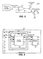
U.S. Patent No. 5,828,892 to Mizuta (hereafter referred to as "Mizuta") discloses amemory card 11 having a power sourcevoltage control circuit 12 that provides a desired working voltage to an I/O (input/output buffer) 13 and a DRAM (dynamic random access memory)device 14, as illustrated inFig. 2 . Thevoltage control circuit 12 provides the desired working voltage (such as 3.3 Volts for example) even when the host voltage Vcc is higher (such as 5.0 Volts for example). -
Fig. 3 shows the implementation of thevoltage control circuit 12 as disclosed in Mizuta. The host voltage is received at aninput 28 that is coupled to afirst window comparator 21 and asecond window comparator 24. Thefirst window comparator 21 turns on afirst MOSFET 22 if the host voltage is within a first range of values such as 4.5 Volts to 5.5 Volts. Thesecond window comparator 24 turns on asecond MOSFET 25 if the host voltage is within a second range of values such as 3.0 Volts to 3.6 Volts. - The
first MOSFET 22 that is turned on couples the host voltage to a DC-DC converter 23 that converts the host voltage in the first range of values down to the working voltage of the DRAM 14 (such as 3.3 Volts for example). Such as stepped down working voltage is generated on anoutput terminal 29. Thesecond MOSFET 25 that is turned on simply couples the host voltage in the second range of values to theoutput terminal 29 as the working voltage of theDRAM 14. - Thus, the
voltage control circuit 12 provides the working voltage that is lower than or equal to the host voltage. Consequently, thememory card 12 may be used with different types of hosts providing host voltages that are greater than or equal to the working voltage of theDRAM 14. - The
memory card 11 of Mizuta accommodates different host voltages to operate with different types of hosts. However, thememory card 11 of Mizuta accommodates a predetermined working voltage of thememory device 14 as the DC-DC converter 23 is fixed for conversion to the predetermined working voltage. With advancement of technology, the working voltage of thememory device 14 may be decreased further and further. Thus, the memory device within a memory card may have one of various working voltages. However, thememory card 11 of Mizuta does not accommodate various working voltages of thememory device 14. -
Patent publication US 5,329,491 against which the preamble is based on, discloses a flash memory card capable of automatically configuring itself to an externally supplied card power voltage. To this end the card comprises a voltage detection circuit to detect the actual value of the external power supply voltage and a card control logic receiving the detection signal of the voltage detection circuit and in response thereof configures a memory array of the card to work with said actual external supply voltage. A voltage conversion circuit provides appropriate device power, program, and erase power supply voltages using the input external supply voltage. - Patent publication
US 5,773,901 discloses a card-receiving host capable of working with different types of cards such as high or low voltage cards and high or low current cards to be selectively inserted into a card-receiving slot. To this end the host is provided with voltage and current sensing switches operated by a corresponding voltage or current discrimination key provided at the card of corresponding type so as to detect the type of card when it is inserted into the slot. The host further comprises means for selectively providing an appropriate operating voltage and/or current to the card in response to the detected card type. - It is the technical problem underlying the invention to provide a semiconductor device card that is easily adaptable for various working voltages.
- The invention solves this problem by providing a semiconductor device card having the device features of
claim 1. Advantageous embodiments of the invention are mentioned in the subclaims, the wording of which is herewith fully incorporated into the description by reference to avoid unnecessary text repetitions. - In an example embodiment of the invention, the semiconductor device is a memory device for the semiconductor device card that is a memory card. In that case, the semiconductor device card includes a memory controller having the working voltage generator.
- The memory controller includes a data processing device, a host interface, and a memory interface. The data processing device controls data transmission between a host and the memory device. The host interface interfaces the data processing device to the host, and the memory interface interfaces the data processing device to the memory device. A host voltage is applied to the host interface, the data processing device, and the memory interface. The working voltage is applied to the memory interface and the memory device.
- In another embodiment of the invention, the working voltage generator generates the working voltage from the host voltage.
- In a further embodiment of the invention, the working voltage generator includes a feed-back path for maintaining the working voltage substantially at the desired level. For example, the feed-back path includes an output node with the working voltage generated thereon. A switch is coupled between the host voltage and the output node. A comparator compares the working voltage and the desired level to turn on the switch for charging/discharging the output node when the working voltage is not equal to the desired level. A reference voltage generator generates a target voltage having the desired level and being coupled to the comparator.
- Alternatively, the working voltage indicator further includes at least one fuse circuit coupled to the multiplexer, and a respective logical state of each output of the fuse circuit is set to indicate the selected target voltage.
- In another embodiment of the invention, the working voltage indicator includes a voltage select decoder that asserts one of a voltage up signal, a voltage down signal, and a voltage pass signal from comparing the host voltage and the working voltage. A first voltage generator generates the working voltage boosted from the host voltage when the voltage up signal is asserted to indicate that the desired level of the working voltage is greater than the host voltage. A second voltage generator generates the working voltage as the host voltage when the voltage pass signal is asserted to indicate that the desired level of the working voltage is substantially equal to the host voltage. A third voltage generator generates the working voltage stepped down from the host voltage when the voltage down signal is asserted to indicate that the desired level of the working voltage is less than the host voltage.
- In another embodiment of the invention, the working voltage indicator includes a variable resistance block coupled to the output node and having a plurality of metal lines with variable coupling for adjusting the working voltage at the output node.
- In this manner, the working voltage generator generates the working voltage having the desired level that is any of higher than, lower than, or substantially equal to the host voltage. Thus, the semiconductor device card is easily adaptable to accommodate various working voltages of the semiconductor device.
- These and other features and advantages of the invention will be better understood by considering the following detailed description of advantageous embodiments of the invention which is presented with the attached drawings. In the drawings:
-
Fig. 1 shows a block diagram of a memory card interfaced to a host, according to the prior art; -
Fig. 2 shows a block diagram of a memory card that accommodates various host voltages, according to the prior art; -
Fig. 3 shows a block diagram of a voltage control circuit ofFig. 2 , according to the prior art; -
Fig. 4 shows a block diagram of a memory card that is adaptable for accommodating various working voltages of a memory device, according to an embodiment of the invention; -
Fig. 5 shows components of a voltage regulator ofFig. 4 , according to an embodiment of the invention; -
Fig. 6 shows an alternative voltage regulator ofFig. 4 with components for accommodating two possible working voltages of the memory device, according to an embodiment of the invention; -
Fig. 7 shows an alternative voltage regulator ofFig. 4 with components for accommodating four possible working voltages of the memory device, according to an embodiment of the invention; -
Fig. 8 illustrates option pins each having a respective logical state set to indicate a desired level of the working voltage inFig. 7 , according to an embodiment of the invention; -
Fig. 9 illustrates fuse circuits each having an output with a respective logical state set to indicate a desired level of the working voltage inFig. 7 , according to another embodiment of the invention; -
Fig. 10 illustrates a voltage regulator ofFig. 4 with a variable resistance block for providing an adjustable working voltage, according to an embodiment of the invention; and -
Fig. 11 illustrates a voltage regulator ofFig. 4 that generates the working voltage that is any of greater than, substantially equal to, or less than the host voltage, according to another embodiment of the invention. - The figures referred to herein are drawn for clarity of illustration and are not necessarily drawn to scale. Elements having the same reference number in
Figs. 1, 2, 3 ,4 ,5 ,6 ,7 ,8 ,9, 10 , and11 refer to elements having similar structure and function. - The invention is described in the following for a memory card. However, the invention may in general be used for any type of semiconductor device card.
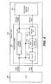
- Referring to
Fig. 4 , asemiconductor card 202 of an embodiment of the invention transmits data between asemiconductor device 204 and ahost 206. Thesemiconductor device 204 is a non-volatile memory device such as a flash memory device, an EEPROM (electrically erasable programmable read only memory), a PRAM (phase-change random access memory), a MRAM (magnetic random access memory), or a FRAM (ferro-electric random access memory), in one embodiment of the invention. - In the case that the
memory device 204 is a flash memory device, thememory card 202 is referred to as a "flash card". Such flash cards are of many types such as MMC (multi-media card), SD (security device), CF (contact flash), or memory sticks depending on the manufacturer or the application. - The
host 206 that uses thememory card 202 to particular advantage may be common portable devices such as MP3 players, camcorders, digital cameras, PDAs (personal digital assistants), and mobile products. However, the invention may be practiced when thesemiconductor card 202 is for any type ofsemiconductor device 204 and any type ofhost 206. - Further referring to
Fig. 4 , thememory card 202 includes amemory controller 208 with avoltage regulator 210, a host I/F (interface) 212, adata processing device 214, and a memory I/F (interface) 216. The host I/F 212 interfaces thememory controller 208 to thehost 206, and the memory I/F 216 interfaces thememory controller 208 to thememory device 204. Thedata processing device 214 controls operation of theinterfaces memory device 204 and thehost 206. - The
voltage regulator 210 receives the host voltage from thehost 206 and generates a working voltage coupled to thememory device 204 and the memory I/F 216, in an embodiment of the invention. The host voltage is coupled to the host I/F 212, thedata processing device 214, and the memory I/F 216, in an embodiment of the invention. - Referring to
Figs. 4 and5 , thevoltage regulator 210 is a working voltage generator in one embodiment of the invention. InFig. 5 , thevoltage regulator 210 includes areference voltage generator 220 that generates a target voltage coupled to a negative input of acomparator 222. The output of thecomparator 222 is coupled to the gate of aPMOSFET 224 having a source coupled to the host voltage from thehost 206. - The drain of the
PMOSFET 224 is coupled to the positive input of thecomparator 222 via a feed-back path 226. The drain of thePMOSFET 224 forms anoutput node 228 having the working voltage generated thereon. Adecoupling capacitor 230 is coupled between theoutput node 228 and a low voltage source VSS which is a ground node of thehost 206 in one embodiment of the invention. - During operation of the voltage regulator of
Fig. 5 , thereference voltage generator 220 generates a target voltage that has the desired level (such as 1.8 Volts for example) of the working voltage to be generated at theoutput node 228. The level of the working voltage generated at theoutput node 228 is compared to the target voltage from thereference voltage generator 220. - Upon power-up, if the level of the working voltage is less than the target voltage, the
PMOSFET 224 is turned on by the negative output of thecomparator 222 to charge up theoutput node 228 for increasing the working voltage. When the working voltage at theoutput node 228 reaches the target voltage, the positive output of thecomparator 222 turns off thePMOSFET 224. - In this manner, the feed-
back path 226 maintains the working voltage at theoutput node 228 to be substantially equal to the target voltage from thereference voltage generator 220. Thus, the working voltage supplied to thememory device 204 has the desired level for any host voltage (such as 3.3 Volts inFig. 5 for example) greater than the desired level of the working voltage. -
Fig. 6 shows an alternative embodiment of thevoltage regulator 210 including a workingvoltage indicator 240 and a workingvoltage generator 242. The workingvoltage indicator 240 includes a firstreference voltage generator 244 for generating a first target voltage with a first level (2.7 Volts for example). The workingvoltage indicator 240 includes a secondreference voltage generator 246 for generating a second target voltage with a second level (1.8 Volts for example). - The working
voltage indicator 240 further includes amultiplexer 248 that inputs the target voltages from the first and secondreference voltage generators reference voltage generators comparator 222. - The working
voltage generator 242 ofFig. 6 operates similarly with that ofFig. 5 to generate the working voltage at theoutput node 228 having the desired level of the selected target voltage from themultiplexer 248. In this manner, the workingvoltage indicator 240 ofFig. 6 allows for flexibility in the working voltage of thememory device 204. With such a workingvoltage indicator 240, the desired level of the working voltage used by thememory device 204 may vary between the two target voltages from thereference voltage generators -
Fig. 7 shows another embodiment of thevoltage regulator 210 having the workingvoltage generator 242 similar to that inFig. 6 . A workingvoltage indicator 250 ofFig. 7 includes first, second, third, and fourth reference voltage generators 252, 254, 256, and 258, respectively. Each of the reference voltage generators 252, 254, 256, and 258 generates a respective target voltage, such as 5.0 Volts, 3.3 Volts, 2.7 Volts, and 1.8 Volts, respectively, for example. - Such target voltages from the reference voltage generators 252, 254, 256, and 258 are input by a
multiplexer 260 that selects one of such target voltages as a selected target voltage coupled to the negative input of thecomparator 222. Themultiplexer 260 selects one of the target voltages from the reference voltage generators 252, 254, 256, and 258 depending on the respective logical state of each of two select signals SEL1 and SEL2. - The working
voltage generator 242 ofFig. 7 operates similarly with that ofFig. 6 to generate the working voltage at theoutput node 228 having the desired level of the selected target voltage from themultiplexer 260. In this manner, the workingvoltage indicator 250 ofFig. 7 allows for flexibility in the working voltage of thememory device 204. With such a workingvoltage indicator 250, the desired level of the working voltage used by thememory device 204 may vary between the four target voltages from the reference voltage generators 252, 254, 256, and 258. -
Fig. 8 illustrates an example mechanism for setting the respective logical state of each of the select signals SEL1 and SEL2 inFig. 7 . Referring toFig. 8 , thememory card 202 includes a first IC (integrated circuit) package of thememory controller 208 and includes a second IC package of thememory device 204. Thememory card 202 includes a plurality of contact pads such as afirst contact pad 262 coupled to the host voltage VDD and asecond contact pad 264 coupled to the host ground VSS. - A
host voltage line 266 coupled to thefirst contact pad 262 and ahost ground line 268 coupled to thesecond contact pad 264 are formed around thememory controller 208. Afirst pin 272 of thememory controller 208 has the first select signal SEL1 applied thereon and is coupled to one of thehost voltage line 266 and thehost ground line 268. If thefirst pin 272 is coupled to thehost voltage line 266, the first select signal SEL1 has a logical high state. If thefirst pin 272 is coupled to thehost ground line 268, the first select signal SEL1 has a logical low state. - Similarly, a second pin 274 of the
memory controller 208 has the second select signal SEL2 applied thereon and is coupled to one of thehost voltage line 266 and thehost ground line 268. If the second pin 274 is coupled to thehost voltage line 266, the second select signal SEL2 has a logical high state. If the second pin 274 is coupled to thehost ground line 268, the second select signal SEL2 has a logical low state. - Referring to
Figs. 7 and8 , during manufacture of thememory card 202, the first andsecond pins 272 and 274 are each coupled to one of thelines multiplexer 260 selects one of the four target voltages from the reference voltage generators 252, 254, 256, and 258 corresponding to the desired level of the working voltage of thememory device 204. In this manner, the first andsecond pins 272 and 274 are set with a respective logical state as part of the workingvoltage indicator 250 for indicating the desired level of the working voltage of thememory device 204. - Further referring to
Fig. 8 , the working voltage generated on theoutput node 228 is applied on athird pin 276 of thememory controller 208 that is coupled to a workingvoltage pin 278 of thememory device 204. Aground pin 280 of thememory device 204 is coupled to thehost ground line 268 such that the working voltage on the workingvoltage pin 278 is with respect to the host ground VSS, in one embodiment of the invention. - Referring to
Figs. 6 and8 , just one pin such as thefirst pin 272 of thememory controller 208 may be used for having the select signal SEL of themultiplexer 248 applied thereon. In that case, thefirst pin 272 is coupled to one of thelines Fig. 6 . -
Fig. 9 shows another mechanism for setting the respective logical state of each of the select signals SEL1 and SEL2 inFig. 7 .Fig. 9 shows afirst fuse circuit 282 and asecond fuse circuit 287 coupled to a power-upinitialization signal generator 285 coupled between the host voltage VDD and the host ground VSS. Upon power up, theinitialization signal generator 285 generates a biasing voltage VCCH with a logical high state. - The
first fuse circuit 282 includes afuse 284 coupled to a drain of aPMOSFET 286 at afirst node 288. ThePMOSFET 228 has a source coupled to the host voltage VDD and a gate having the VCCH bias applied thereon. AnNMOSFET 290 has a drain coupled to asecond node 292 of thefuse 284, a source coupled to the host ground node VSS, and a gate having the VCCH bias applied thereon. - The
first fuse circuit 282 also includes a latch 294 of a loop ofinverters first node 288 of thefuse 284. The output of the latch 294 generates the first select signal SEL1. During operation of thefirst fuse circuit 282, when thefuse 284 is cut to be open-circuited, the SEL1 signal is a logical low state. Alternatively, when thefuse 284 is not cut, the SEL1 signal is a logical high state. - The
fuse 284 of thefirst fuse circuit 282 is cut or left not cut for setting the logical state of the SEL1 signal. Thesecond fuse circuit 287 is similar to thefirst fuse circuit 282 with another fuse within thesecond fuse circuit 287 that is cut or left not cut for setting the logical state of the SEL2 signal. - Referring to
Figs. 7 and9 , during manufacture of thememory card 202, the respective fuse within each of the first andsecond fuse circuits multiplexer 260 selects one of the four target voltages from the reference voltage generators 252, 254, 256, and 258 corresponding to the desired level of the working voltage of thememory device 204. In this manner, the respective fuse within each of the first andsecond fuse circuits voltage indicator 250 for indicating the desired level of the working voltage of thememory device 204. -
Fig. 10 shows an alternative embodiment of thevoltage regulator 210 with a working voltage generated at theoutput node 228. The level of such a working voltage is adjustable with variable coupling of a plurality ofmetal lines variable resistance block 320. Elements having the same reference number inFigs. 5 and10 refer to elements having similar structure and function. - In
Fig. 10 however, a plurality of resistors are coupled from the drain of thePMOSFET 224. Afirst resistor 308 is coupled between the drain of thePMOSFET 224 and a feed-back path node 310. Asecond resistor 310 is coupled between the feed-back path node 310 and afirst metal line 302. Athird resistor 314 is coupled between thefirst metal line 302 and asecond metal line 304. Afourth resistor 316 is coupled between thesecond metal line 304 and athird metal line 306 which is also coupled to the host ground node VSS. - Any of the
metal lines variable resistance block 320. For example, if thefirst metal line 302 is connected to thethird metal line 306, the resistance through theresistance block 320 is zero. If thesecond metal line 304 is connected to thethird metal line 306, the resistance through theresistance block 320 is the resistance of thethird resistor 314. If thefirst metal line 302 is connected to thesecond metal line 304, the resistance through theresistance block 320 is the resistance of thefourth resistor 316. - In any case, a voltage substantially similar to the reference voltage generated by the
reference voltage generator 220 is generated at the feed-back path node 310. By varying the resistance of theresistance block 320, a variable level of current flows through theresistors output node 228 may be varied. In this manner, the connection of themetal lines output node 228. Thus, thevoltage regulator 210 ofFig. 10 allows for flexibility in the working voltage of thememory device 204. -
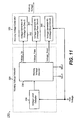
Fig. 11 shows an alternative embodiment of thevoltage regulator 210 having a workingvoltage indicator 330 and a workingvoltage generator 332. The working voltage indicator includes a hostvoltage level detector 334 and a workingvoltage decoder 336. The hostvoltage level detector 334 indicates the level of the host voltage VDD to the workingvoltage decoder 336. - The working
voltage decoder 336 inputs first and second select signals SEL1 and SEL2 each having a respective logical state for indicating a desired level of the working voltage of thememory device 204. The first and second select signals SEL1 and SEL2 may be generated as described in reference toFigs. 8 or9 . The workingvoltage decoder 336 compares the level of the host voltage VDD and the desired level of the working voltage of thememory device 204 and asserts one of a voltage up signal, a voltage pass signal, and a voltage down signal. - The working
voltage decoder 336 asserts the voltage up signal if the desired level of the working voltage is greater than the level of the host voltage VDD. Alternatively, the workingvoltage decoder 336 asserts the voltage pass signal if the desired level of the working voltage is substantially equal to the level of the host voltage VDD. Finally, workingvoltage decoder 336 asserts the voltage down signal if the desired level of the working voltage is less than the level of the host voltage VDD. - The working voltage generator includes first, second, and
third voltage generators voltage decoder 336. - If the voltage up signal is asserted, the first voltage generator 342 (i.e., a voltage up circuit) is activated for generating the working voltage boosted from the host voltage. Alternatively, if the voltage pass signal is asserted, the second voltage generator 344 (i.e., a voltage pass circuit) is activated for generating the working voltage as the host voltage.
- Finally, if the voltage down signal is asserted, the third voltage generator 346 (i.e., a voltage down circuit) is activated for generating the working voltage that is stepped down from the host voltage. In this manner, the
voltage regulator 210 ofFig. 11 allows for the desired level of the working voltage of thememory device 204 to be any of greater than, substantially equal to, or less than the level of the host voltage. - The foregoing is by way of example only and is not intended to be limiting. For example, the invention has been described in reference to the
memory device 204 for thememory card 202. However, the invention may be used for generating the working voltage of any other type of semiconductor device on any other type of semiconductor device card. In addition, any number of elements illustrated and described herein are by way of example only. Furthermore, any values of voltages illustrated and described herein are by way of example only. For example, a negative host voltage with an NMOSFET may be used for discharging theoutput node 228 to a negative working voltage in thevoltage regulator 210 ofFig. 5 . - The invention is limited only as defined in the following claims and equivalents thereof.
Claims (16)
- A semiconductor device card (202) comprising:a semiconductor device (204);a working voltage indicator (240) that is set to indicate a desired level of a working voltage corresponding to the semiconductor device (204) and to output a corresponding target voltage signal; anda working voltage generator (242);characterized in thatthe semiconductor device (204) is configured to operate at said desired level of the working voltage independent of whether a host voltage supplied to the semiconductor device card has a different voltage level;the working voltage generator (242) is coupled to the semiconductor device and receives the target voltage signal from the working voltage indicator an able to generate the working voltage for the semiconductor device having said desired level; andthe working voltage indicator (240) includes a plurality of reference voltage generators (244, 246) for generating respectively different target voltages at least one of which being different from the host voltage supplied to the card, a multiplexer (248) for coupling a selected one of the target voltages having the desired level from one of the reference voltage generators to the working voltage generator, and at least one option pin coupled to the multiplexer, wherein a respective logical state of each option pin (SEL, 272, 274) is set to indicate the desired level of the working voltage.
- The semiconductor device card of claim 1, wherein the working voltage generator includes a feed-back path (226) for maintaining the working voltage substantially at said desired level.
- The semiconductor device card of claim 1 or 2, wherein the working voltage generator includes a decoupling capacitor (230) coupled to an output node at which the working voltage is provided.
- The semiconductor device card of any of claims 1 to 3, wherein the working voltage indicator includes a variable resistance block (320) coupled to an output node at which the working voltage is provided and having a plurality of metal lines (302, 304, 306) with variable coupling for adjusting the working voltage at the output node.
- The semiconductor device card of any of claims 1 to 4, wherein the working voltage generator generates the working voltage from a host voltage.
- The semiconductor device card of any of claims 2 to 5, wherein the feed-back path includes:an output node (228) with the working voltage generated thereon;a switch (224) coupled between a voltage source and the output node; anda comparator (222) for comparing the working voltage and the desired level to turn on the switch for charging/discharging the output node when the working voltage is not equal to the desired level.
- The semiconductor device card of claim 6, wherein the voltage generator further includes a reference voltage generator (220) for generating a target voltage having the desired level and being coupled to the comparator.
- The semiconductor device card of claim 6 or 7, wherein the voltage source is a host providing a host voltage.
- The semiconductor device card of any of claims 1 to 8, wherein the working voltage generator (242) is adapted to generate the working voltage from a host voltage with the desired level being any of higher than, lower than, and substantially equal to the host voltage.
- The semiconductor device card of claim 9, further comprising:a voltage select decoder (336) that asserts one of a voltage up signal, a voltage down signal, and a voltage pass signal from comparing the host voltage and the working voltage;wherein the working voltage generator (332) includes:a first voltage generator (342) for generating the working voltage boosted from the host voltage when the voltage up signal is asserted to indicate that the desired level of the working voltage is greater than the host voltage;a second voltage generator (344) for generating the working voltage as the host voltage when the voltage pass signal is asserted to indicate that the desired level of the working voltage is substantially equal to the host voltage; anda third voltage generator (346) for generating the working voltage stepped down from the host voltage when the voltage down signal is asserted to indicate that the desired level of the working voltage is less than the host voltage.
- The semiconductor device card of any of claims 1 to 10, wherein the working voltage indicator further includes at least one fuse circuit (282, 287) coupled to the multiplexer or voltage select decoder, wherein a respective logical state of each output of the fuse circuit is set to indicate the selected target voltage or desired level of the working voltage.
- The semiconductor device card of any of claims 1 to 11, further comprising a memory controller including the working voltage generator.
- The semiconductor device card of claim 12, wherein the memory controller further includes:a data processing device for controlling data transmission between a host and the memory device;a host interface for interfacing the data processing device to the host; anda memory interface for interfacing the data processing device to the memory device;wherein a host voltage is applied to the host interface, the data processing device, and the memory interface;and wherein the working voltage is applied to the memory interface and the memory device.
- The semiconductor device card of any of claims 1 to 13, wheren the semiconductor device is a memory device for the semiconductor device card that is a memory card.
- The semiconductor device card of claim 14, wherein the memory device is nonvolatile.
- The semiconductor device card of claim 14 or 15, further comprising:a host interface for interfacing the data processing device to the host; anda memory interface for interfacing the data processing device to the memory device;wherein the host voltage is applied to the host interface and the memory interface;and wherein the working voltage is applied to the memory interface.
Priority Applications (1)
| Application Number | Priority Date | Filing Date | Title |
|---|---|---|---|
| EP07013426.7A EP1843162B1 (en) | 2003-12-31 | 2004-12-22 | Semiconductor device card |
Applications Claiming Priority (4)
| Application Number | Priority Date | Filing Date | Title |
|---|---|---|---|
| KR2003101270 | 2003-12-31 | ||
| KR1020030101270A KR100884235B1 (en) | 2003-12-31 | 2003-12-31 | Nonvolatile memory card |
| US10/960,733 US7453741B2 (en) | 2003-12-31 | 2004-10-07 | Semiconductor device card providing multiple working voltages |
| US960733 | 2004-10-07 |
Related Child Applications (2)
| Application Number | Title | Priority Date | Filing Date |
|---|---|---|---|
| EP07013426.7A Division-Into EP1843162B1 (en) | 2003-12-31 | 2004-12-22 | Semiconductor device card |
| EP07013426.7A Division EP1843162B1 (en) | 2003-12-31 | 2004-12-22 | Semiconductor device card |
Publications (3)
| Publication Number | Publication Date |
|---|---|
| EP1551031A2 EP1551031A2 (en) | 2005-07-06 |
| EP1551031A3 EP1551031A3 (en) | 2006-07-19 |
| EP1551031B1 true EP1551031B1 (en) | 2015-09-16 |
Family
ID=34576059
Family Applications (2)
| Application Number | Title | Priority Date | Filing Date |
|---|---|---|---|
| EP07013426.7A Active EP1843162B1 (en) | 2003-12-31 | 2004-12-22 | Semiconductor device card |
| EP04030397.6A Active EP1551031B1 (en) | 2003-12-31 | 2004-12-22 | Semiconductor device card |
Family Applications Before (1)
| Application Number | Title | Priority Date | Filing Date |
|---|---|---|---|
| EP07013426.7A Active EP1843162B1 (en) | 2003-12-31 | 2004-12-22 | Semiconductor device card |
Country Status (5)
| Country | Link |
|---|---|
| US (1) | US7453741B2 (en) |
| EP (2) | EP1843162B1 (en) |
| JP (1) | JP4676752B2 (en) |
| KR (1) | KR100884235B1 (en) |
| CN (1) | CN1637925B (en) |
Families Citing this family (28)
| Publication number | Priority date | Publication date | Assignee | Title |
|---|---|---|---|---|
| US7226857B2 (en) | 2004-07-30 | 2007-06-05 | Micron Technology, Inc. | Front-end processing of nickel plated bond pads |
| US7313019B2 (en) * | 2004-12-21 | 2007-12-25 | Intel Corporation | Step voltage generation |
| US7864615B2 (en) * | 2005-02-25 | 2011-01-04 | Kingston Technology Corporation | Flash memory controller utilizing multiple voltages and a method of use |
| US7355905B2 (en) | 2005-07-01 | 2008-04-08 | P.A. Semi, Inc. | Integrated circuit with separate supply voltage for memory that is different from logic circuit supply voltage |
| TWI319160B (en) * | 2005-07-11 | 2010-01-01 | Via Tech Inc | Memory card capable of supporting various voltage supply and control chip and method of supporting voltage thereof |
| WO2007017926A1 (en) * | 2005-08-08 | 2007-02-15 | Spansion Llc | Semiconductor device and control method thereof |
| TW200709213A (en) * | 2005-08-24 | 2007-03-01 | Siliconmotion Inc | A memory system with two voltage sources |
| WO2007038944A1 (en) * | 2005-09-21 | 2007-04-12 | Freescale Semiconductor, Inc. | An integrated circuit and a method for selecting a voltage in an integrated circuit |
| KR101177555B1 (en) * | 2006-02-01 | 2012-08-27 | 삼성전자주식회사 | Memory Card and DATA driving Method thereof and Memory Card System |
| JP4843472B2 (en) * | 2006-03-13 | 2011-12-21 | 株式会社東芝 | Voltage generation circuit |
| US7656735B2 (en) * | 2006-09-29 | 2010-02-02 | Sandisk Corporation | Dual voltage flash memory methods |
| US7675802B2 (en) * | 2006-09-29 | 2010-03-09 | Sandisk Corporation | Dual voltage flash memory card |
| US20090020608A1 (en) * | 2007-04-05 | 2009-01-22 | Bennett Jon C R | Universal memory socket and card and system for using the same |
| US20080273391A1 (en) * | 2007-05-04 | 2008-11-06 | Microchip Technology Incorporated | Regulator Bypass Start-Up in an Integrated Circuit Device |
| US7764547B2 (en) * | 2007-12-20 | 2010-07-27 | Sandisk Corporation | Regulation of source potential to combat cell source IR drop |
| US7701761B2 (en) * | 2007-12-20 | 2010-04-20 | Sandisk Corporation | Read, verify word line reference voltage to track source level |
| CN101910972B (en) * | 2008-02-29 | 2013-03-20 | 松下电器产业株式会社 | Interface device for host device, interface device for slave device, host device, slave device, communication system and interface voltage switching method |
| JP5106219B2 (en) * | 2008-03-19 | 2012-12-26 | 株式会社東芝 | Memory device, host device, memory system, memory device control method, host device control method, and memory system control method |
| US8289798B2 (en) * | 2010-03-17 | 2012-10-16 | International Business Machines Corporation | Voltage regulator bypass in memory device |
| US9710031B2 (en) * | 2010-12-30 | 2017-07-18 | Silicon Laboratories Inc. | Analog interface for a microprocessor-based device |
| TWI514123B (en) * | 2011-01-04 | 2015-12-21 | Richtek Technology Corp | Circuit and method for power path management |
| KR20130107836A (en) * | 2012-03-23 | 2013-10-02 | 에스케이하이닉스 주식회사 | Multi-chip semiconductor apparatus |
| US8804449B2 (en) | 2012-09-06 | 2014-08-12 | Micron Technology, Inc. | Apparatus and methods to provide power management for memory devices |
| TWI508092B (en) * | 2013-04-25 | 2015-11-11 | Winbond Electronics Corp | Power management devices and methods |
| US9256278B2 (en) | 2013-08-20 | 2016-02-09 | Winbond Electronics Corp. | Devices and methods for multi-core memory |
| KR102107072B1 (en) * | 2013-11-29 | 2020-05-07 | 에스케이하이닉스 주식회사 | System including memory controller which manages power of memory |
| CN105097038B (en) * | 2015-06-23 | 2023-06-27 | 兆易创新科技集团股份有限公司 | Voltage output method and device |
| WO2022073177A1 (en) * | 2020-10-09 | 2022-04-14 | Micron Technology, Inc. | Improved power supply for memory device |
Family Cites Families (26)
| Publication number | Priority date | Publication date | Assignee | Title |
|---|---|---|---|---|
| KR100231393B1 (en) | 1991-04-18 | 1999-11-15 | 나시모토 류조 | Semiconductor integrated circuit |
| JP2785548B2 (en) * | 1991-10-25 | 1998-08-13 | 日本電気株式会社 | Semiconductor memory |
| US5267218A (en) | 1992-03-31 | 1993-11-30 | Intel Corporation | Nonvolatile memory card with a single power supply input |
| JP3477781B2 (en) | 1993-03-23 | 2003-12-10 | セイコーエプソン株式会社 | IC card |
| JP3085824B2 (en) * | 1993-05-20 | 2000-09-11 | 富士写真フイルム株式会社 | Memory controller |
| US5329491A (en) | 1993-06-30 | 1994-07-12 | Intel Corporation | Nonvolatile memory card with automatic power supply configuration |
| JPH08153388A (en) | 1994-11-28 | 1996-06-11 | Mitsubishi Electric Corp | Semiconductor storage |
| US5627416A (en) | 1995-07-21 | 1997-05-06 | Itt Corporation | Multi-voltage IC card host |
| US5596532A (en) | 1995-10-18 | 1997-01-21 | Sandisk Corporation | Flash EEPROM self-adaptive voltage generation circuit operative within a continuous voltage source range |
| CN1202255A (en) * | 1995-11-13 | 1998-12-16 | 勒克萨微型系统股份有限公司 | Automatic voltage detection in multiple voltage applications |
| KR0163896B1 (en) * | 1995-12-20 | 1998-12-15 | 김광호 | Power supply device |
| JPH09231339A (en) | 1996-02-27 | 1997-09-05 | Mitsubishi Electric Corp | Memory card |
| JP3493096B2 (en) * | 1996-06-07 | 2004-02-03 | 株式会社東芝 | Semiconductor integrated circuit, IC card, and IC card system |
| KR19980081575A (en) * | 1997-04-21 | 1998-11-25 | 윤종용 | Smart card with adjustable level of external input voltage |
| US6114878A (en) * | 1998-02-13 | 2000-09-05 | Micron Technology, Inc. | Circuit for contact pad isolation |
| JP2001337757A (en) * | 2000-05-29 | 2001-12-07 | Seiko Epson Corp | Electronic device and card pc used for the device |
| JP4043703B2 (en) * | 2000-09-04 | 2008-02-06 | 株式会社ルネサステクノロジ | Semiconductor device, microcomputer, and flash memory |
| US6434044B1 (en) * | 2001-02-16 | 2002-08-13 | Sandisk Corporation | Method and system for generation and distribution of supply voltages in memory systems |
| JP4156863B2 (en) * | 2002-05-14 | 2008-09-24 | 株式会社ルネサステクノロジ | Semiconductor integrated circuit and IC card |
| JP2004071095A (en) * | 2002-08-08 | 2004-03-04 | Renesas Technology Corp | Semiconductor memory |
| US7212067B2 (en) * | 2003-08-01 | 2007-05-01 | Sandisk Corporation | Voltage regulator with bypass for multi-voltage storage system |
| JP4653960B2 (en) * | 2003-08-07 | 2011-03-16 | ルネサスエレクトロニクス株式会社 | Memory card and nonvolatile memory embedded microcomputer |
| US7064602B2 (en) * | 2004-05-05 | 2006-06-20 | Rambus Inc. | Dynamic gain compensation and calibration |
| US7068019B1 (en) * | 2005-03-23 | 2006-06-27 | Mediatek Inc. | Switchable linear regulator |
| US7173854B2 (en) * | 2005-04-01 | 2007-02-06 | Sandisk Corporation | Non-volatile memory and method with compensation for source line bias errors |
| US7170784B2 (en) * | 2005-04-01 | 2007-01-30 | Sandisk Corporation | Non-volatile memory and method with control gate compensation for source line bias errors |
-
2003
- 2003-12-31 KR KR1020030101270A patent/KR100884235B1/en active IP Right Grant
-
2004
- 2004-10-07 US US10/960,733 patent/US7453741B2/en active Active
- 2004-12-14 JP JP2004361728A patent/JP4676752B2/en active Active
- 2004-12-22 EP EP07013426.7A patent/EP1843162B1/en active Active
- 2004-12-22 EP EP04030397.6A patent/EP1551031B1/en active Active
- 2004-12-31 CN CN2004100817818A patent/CN1637925B/en active Active
Also Published As
| Publication number | Publication date |
|---|---|
| US20050141317A1 (en) | 2005-06-30 |
| KR100884235B1 (en) | 2009-02-17 |
| CN1637925B (en) | 2012-03-21 |
| EP1843162B1 (en) | 2015-12-09 |
| EP1551031A2 (en) | 2005-07-06 |
| EP1843162A1 (en) | 2007-10-10 |
| EP1551031A3 (en) | 2006-07-19 |
| US7453741B2 (en) | 2008-11-18 |
| JP2005196754A (en) | 2005-07-21 |
| JP4676752B2 (en) | 2011-04-27 |
| KR20050069303A (en) | 2005-07-05 |
| CN1637925A (en) | 2005-07-13 |
Similar Documents
| Publication | Publication Date | Title |
|---|---|---|
| EP1551031B1 (en) | Semiconductor device card | |
| US9343176B2 (en) | Low-pin-count non-volatile memory interface with soft programming capability | |
| US8157180B2 (en) | Integrated circuit device with multiple communication modes and operating method thereof | |
| JP4734243B2 (en) | Voltage regulator with bypass for a multi-stage voltage storage system | |
| US7495989B2 (en) | Portable data storage apparatus | |
| US6842384B2 (en) | Nonvolatile semiconductor memory with power-up read mode | |
| KR100395770B1 (en) | Novolatile flash memory device usable as a boot-up memory in a system and method of operating the same | |
| US7564279B2 (en) | Power on reset circuitry in electronic systems | |
| JP2006512887A (en) | High voltage ripple reduction and board protection | |
| KR101443419B1 (en) | Method and circuit for preventing high voltage memory disturb | |
| KR20020039340A (en) | Electric/electronic circuit device | |
| US5706242A (en) | Semiconductor device having a controllable voltage supply | |
| US9323260B2 (en) | Internal voltage generation circuits and semiconductor devices including the same | |
| US7738310B2 (en) | Fuse data acquisition | |
| US6885215B1 (en) | Voltage detector circuit with a programmable threshold point | |
| CN113345494B (en) | Semiconductor device with a semiconductor device having a plurality of semiconductor chips | |
| CN114079448A (en) | Device configured to perform power gating operations | |
| EP1584936B1 (en) | Test terminal negation circuit | |
| KR20090022622A (en) | Rfid device with non-volatile ferroelectric memory | |
| US9947374B2 (en) | Semiconductor devices and semiconductor systems including the same |
Legal Events
| Date | Code | Title | Description |
|---|---|---|---|
| PUAI | Public reference made under article 153(3) epc to a published international application that has entered the european phase |
Free format text: ORIGINAL CODE: 0009012 |
|
| AK | Designated contracting states |
Kind code of ref document: A2 Designated state(s): AT BE BG CH CY CZ DE DK EE ES FI FR GB GR HU IE IS IT LI LT LU MC NL PL PT RO SE SI SK TR |
|
| AX | Request for extension of the european patent |
Extension state: AL BA HR LV MK YU |
|
| RIC1 | Information provided on ipc code assigned before grant |
Ipc: G11C 5/14 20060101AFI20050428BHEP Ipc: G11C 16/30 20060101ALI20060315BHEP |
|
| PUAL | Search report despatched |
Free format text: ORIGINAL CODE: 0009013 |
|
| AK | Designated contracting states |
Kind code of ref document: A3 Designated state(s): AT BE BG CH CY CZ DE DK EE ES FI FR GB GR HU IE IS IT LI LT LU MC NL PL PT RO SE SI SK TR |
|
| AX | Request for extension of the european patent |
Extension state: AL BA HR LV MK YU |
|
| 17P | Request for examination filed |
Effective date: 20060912 |
|
| 17Q | First examination report despatched |
Effective date: 20061016 |
|
| AKX | Designation fees paid |
Designated state(s): DE FR GB |
|
| 17Q | First examination report despatched |
Effective date: 20061016 |
|
| RAP1 | Party data changed (applicant data changed or rights of an application transferred) |
Owner name: SAMSUNG ELECTRONICS CO., LTD. |
|
| GRAP | Despatch of communication of intention to grant a patent |
Free format text: ORIGINAL CODE: EPIDOSNIGR1 |
|
| INTG | Intention to grant announced |
Effective date: 20150324 |
|
| GRAS | Grant fee paid |
Free format text: ORIGINAL CODE: EPIDOSNIGR3 |
|
| GRAA | (expected) grant |
Free format text: ORIGINAL CODE: 0009210 |
|
| AK | Designated contracting states |
Kind code of ref document: B1 Designated state(s): DE FR GB |
|
| REG | Reference to a national code |
Ref country code: GB Ref legal event code: FG4D |
|
| REG | Reference to a national code |
Ref country code: DE Ref legal event code: R096 Ref document number: 602004047902 Country of ref document: DE |
|
| REG | Reference to a national code |
Ref country code: DE Ref legal event code: R097 Ref document number: 602004047902 Country of ref document: DE |
|
| PLBE | No opposition filed within time limit |
Free format text: ORIGINAL CODE: 0009261 |
|
| STAA | Information on the status of an ep patent application or granted ep patent |
Free format text: STATUS: NO OPPOSITION FILED WITHIN TIME LIMIT |
|
| 26N | No opposition filed |
Effective date: 20160617 |
|
| GBPC | Gb: european patent ceased through non-payment of renewal fee |
Effective date: 20151222 |
|
| REG | Reference to a national code |
Ref country code: FR Ref legal event code: ST Effective date: 20160831 |
|
| PG25 | Lapsed in a contracting state [announced via postgrant information from national office to epo] |
Ref country code: GB Free format text: LAPSE BECAUSE OF NON-PAYMENT OF DUE FEES Effective date: 20151222 |
|
| PG25 | Lapsed in a contracting state [announced via postgrant information from national office to epo] |
Ref country code: FR Free format text: LAPSE BECAUSE OF NON-PAYMENT OF DUE FEES Effective date: 20151231 |
|
| P01 | Opt-out of the competence of the unified patent court (upc) registered |
Effective date: 20230520 |
|
| PGFP | Annual fee paid to national office [announced via postgrant information from national office to epo] |
Ref country code: DE Payment date: 20231024 Year of fee payment: 20 |