EP1957992B1 - Diagnostic system for power converter - Google Patents
Diagnostic system for power converter Download PDFInfo
- Publication number
- EP1957992B1 EP1957992B1 EP06839073A EP06839073A EP1957992B1 EP 1957992 B1 EP1957992 B1 EP 1957992B1 EP 06839073 A EP06839073 A EP 06839073A EP 06839073 A EP06839073 A EP 06839073A EP 1957992 B1 EP1957992 B1 EP 1957992B1
- Authority
- EP
- European Patent Office
- Prior art keywords
- dev
- overcurrent
- signals
- amplifier
- power
- Prior art date
- Legal status (The legal status is an assumption and is not a legal conclusion. Google has not performed a legal analysis and makes no representation as to the accuracy of the status listed.)
- Active
Links
- 238000005259 measurement Methods 0.000 claims abstract description 44
- 238000006243 chemical reaction Methods 0.000 claims description 32
- 238000007619 statistical method Methods 0.000 claims description 10
- 230000002238 attenuated effect Effects 0.000 claims description 9
- 230000003321 amplification Effects 0.000 claims description 8
- 238000003199 nucleic acid amplification method Methods 0.000 claims description 8
- 238000004458 analytical method Methods 0.000 abstract description 16
- 238000012360 testing method Methods 0.000 description 60
- 238000001514 detection method Methods 0.000 description 22
- 230000000875 corresponding effect Effects 0.000 description 17
- 238000010586 diagram Methods 0.000 description 13
- 238000000034 method Methods 0.000 description 8
- 230000002950 deficient Effects 0.000 description 7
- 230000007547 defect Effects 0.000 description 5
- 230000006872 improvement Effects 0.000 description 5
- 230000008901 benefit Effects 0.000 description 4
- 238000013461 design Methods 0.000 description 4
- 238000003745 diagnosis Methods 0.000 description 4
- 210000002381 plasma Anatomy 0.000 description 4
- 230000001052 transient effect Effects 0.000 description 4
- 238000001816 cooling Methods 0.000 description 3
- 238000009826 distribution Methods 0.000 description 3
- 238000009434 installation Methods 0.000 description 3
- 230000000670 limiting effect Effects 0.000 description 3
- 239000002184 metal Substances 0.000 description 3
- 230000005236 sound signal Effects 0.000 description 3
- 239000010752 BS 2869 Class D Substances 0.000 description 2
- 230000009471 action Effects 0.000 description 2
- 230000002902 bimodal effect Effects 0.000 description 2
- 238000002405 diagnostic procedure Methods 0.000 description 2
- 230000000694 effects Effects 0.000 description 2
- 238000001914 filtration Methods 0.000 description 2
- 230000001965 increasing effect Effects 0.000 description 2
- 238000009413 insulation Methods 0.000 description 2
- 230000007257 malfunction Effects 0.000 description 2
- 238000004519 manufacturing process Methods 0.000 description 2
- 230000008569 process Effects 0.000 description 2
- 229920006395 saturated elastomer Polymers 0.000 description 2
- 238000012935 Averaging Methods 0.000 description 1
- 238000005299 abrasion Methods 0.000 description 1
- 238000013459 approach Methods 0.000 description 1
- 230000003190 augmentative effect Effects 0.000 description 1
- 238000009529 body temperature measurement Methods 0.000 description 1
- 239000003990 capacitor Substances 0.000 description 1
- 230000002596 correlated effect Effects 0.000 description 1
- 230000006378 damage Effects 0.000 description 1
- 230000003292 diminished effect Effects 0.000 description 1
- 230000005684 electric field Effects 0.000 description 1
- 238000002474 experimental method Methods 0.000 description 1
- 230000036039 immunity Effects 0.000 description 1
- 230000001939 inductive effect Effects 0.000 description 1
- 239000011810 insulating material Substances 0.000 description 1
- 238000011835 investigation Methods 0.000 description 1
- 230000007774 longterm Effects 0.000 description 1
- 238000013507 mapping Methods 0.000 description 1
- 239000000463 material Substances 0.000 description 1
- 238000012544 monitoring process Methods 0.000 description 1
- 230000000737 periodic effect Effects 0.000 description 1
- 238000012545 processing Methods 0.000 description 1
- 230000001681 protective effect Effects 0.000 description 1
- 230000001603 reducing effect Effects 0.000 description 1
- 230000002829 reductive effect Effects 0.000 description 1
- 230000001105 regulatory effect Effects 0.000 description 1
- 230000004044 response Effects 0.000 description 1
- 150000003839 salts Chemical class 0.000 description 1
- 238000005070 sampling Methods 0.000 description 1
- 230000035939 shock Effects 0.000 description 1
- 229910052710 silicon Inorganic materials 0.000 description 1
- 239000010703 silicon Substances 0.000 description 1
- 238000001228 spectrum Methods 0.000 description 1
- 230000003068 static effect Effects 0.000 description 1
- 238000003860 storage Methods 0.000 description 1
- 239000000126 substance Substances 0.000 description 1
- 230000008093 supporting effect Effects 0.000 description 1
- 208000024891 symptom Diseases 0.000 description 1
- 230000026683 transduction Effects 0.000 description 1
- 238000010361 transduction Methods 0.000 description 1
- 230000001960 triggered effect Effects 0.000 description 1
- XLYOFNOQVPJJNP-UHFFFAOYSA-N water Substances O XLYOFNOQVPJJNP-UHFFFAOYSA-N 0.000 description 1
Images


Classifications
-
- G—PHYSICS
- G01—MEASURING; TESTING
- G01R—MEASURING ELECTRIC VARIABLES; MEASURING MAGNETIC VARIABLES
- G01R31/00—Arrangements for testing electric properties; Arrangements for locating electric faults; Arrangements for electrical testing characterised by what is being tested not provided for elsewhere
- G01R31/005—Testing of electric installations on transport means
- G01R31/006—Testing of electric installations on transport means on road vehicles, e.g. automobiles or trucks
- G01R31/007—Testing of electric installations on transport means on road vehicles, e.g. automobiles or trucks using microprocessors or computers
-
- G—PHYSICS
- G01—MEASURING; TESTING
- G01R—MEASURING ELECTRIC VARIABLES; MEASURING MAGNETIC VARIABLES
- G01R19/00—Arrangements for measuring currents or voltages or for indicating presence or sign thereof
- G01R19/25—Arrangements for measuring currents or voltages or for indicating presence or sign thereof using digital measurement techniques
-
- G—PHYSICS
- G01—MEASURING; TESTING
- G01R—MEASURING ELECTRIC VARIABLES; MEASURING MAGNETIC VARIABLES
- G01R31/00—Arrangements for testing electric properties; Arrangements for locating electric faults; Arrangements for electrical testing characterised by what is being tested not provided for elsewhere
- G01R31/50—Testing of electric apparatus, lines, cables or components for short-circuits, continuity, leakage current or incorrect line connections
-
- G—PHYSICS
- G01—MEASURING; TESTING
- G01R—MEASURING ELECTRIC VARIABLES; MEASURING MAGNETIC VARIABLES
- G01R19/00—Arrangements for measuring currents or voltages or for indicating presence or sign thereof
- G01R19/165—Indicating that current or voltage is either above or below a predetermined value or within or outside a predetermined range of values
- G01R19/17—Indicating that current or voltage is either above or below a predetermined value or within or outside a predetermined range of values giving an indication of the number of times this occurs, i.e. multi-channel analysers
-
- G—PHYSICS
- G01—MEASURING; TESTING
- G01R—MEASURING ELECTRIC VARIABLES; MEASURING MAGNETIC VARIABLES
- G01R31/00—Arrangements for testing electric properties; Arrangements for locating electric faults; Arrangements for electrical testing characterised by what is being tested not provided for elsewhere
- G01R31/50—Testing of electric apparatus, lines, cables or components for short-circuits, continuity, leakage current or incorrect line connections
- G01R31/52—Testing for short-circuits, leakage current or ground faults
Landscapes
- Physics & Mathematics (AREA)
- General Physics & Mathematics (AREA)
- Engineering & Computer Science (AREA)
- Computer Hardware Design (AREA)
- Microelectronics & Electronic Packaging (AREA)
- Chemical & Material Sciences (AREA)
- Combustion & Propulsion (AREA)
- Amplifiers (AREA)
- Inverter Devices (AREA)
Abstract
Description
- A portion of the disclosure of this patent document contains material which is subject to copyright protection. The copyright owner has no objection to the facsimile reproduction by anyone of the patent document or the patent disclosure, as it appears in the Patent and Trademark Office patent file or records, but otherwise reserves all copyright rights whatsoever.
- The present invention relates to a diagnostic system for a power converter.
- Audio systems, such as those used in vehicles, may include a variety of system components. Such system components may Include various audio sources, audio signal processors, channel power amplifiers, power supplies, and the like. In vehicle Installations, as well as other Installations, these components are subjected to a variety of conditions that may result in faulty operation of the audio system. Some defects may arise due to faulty installation and/or manufacture of the audio system. For example, non-connected and/or open transducers may occur at the time of manufacture. Other defects may result from longer term exposure to the ambient conditions in which the audio system operates thereby becoming evident only after the audio system has been in operation for a time. Faults resulting from short and open connections as well as defective transducers are not uncommon when the audio system is subject to long term thermal and vibrational stress. For example, channel power amplifiers (or other power converters) may have their outputs shorted to ground, to battery circuits, or to each other.
DE 38 43 507 A discloses a method for measuring clocked currents in an inductive load in a vehicle based on short time current sampling
US 2005/249353 A1 discloses an audio system that allows for the detection of fault conditions by means of a fault detection circuit that monitors an audio output from an audio generation device. In particular, if the audio output is outside an upper or lower predetermined limit a fault condition is detected and a switch will isolate the audio generation circuit.
EP -A- 0 841 570 discloses an automotive audio system wherein connections of speakers are automatically checked and actions of an audio limiting function are monitored to detect shorts. A Ginart et al., in paper entitled "Analysis of the class AD audio amplifier including hysteresis effects", 6 February 299, Applied Power Electronics Conference and Exposition, Fifteenth Annual IEEE New Orleans, pages 1095-1100, describe power amplifiers capable of producing low distortion with high efficiency. The high efficiency is achieved with a combination of an inverter and an analog amplifier, where the inverter provides the power, and the analog amplifier acts as an active filter to correct distortion - Shorts between significantly dissimilar potentials may result in large currents that can activate the protection circuitry of an amplifier. In such situations, any occurrence of an overcurrent event would most likely be the consequence of some form of short on the overloaded output. What is not evident from the overcurrent event signal is the specific nature of the fault. Additional information may be required in order to discern the nature of the fault. Therefore, a need exists to better diagnose the cause of overcurrents or other errors in an audio system.
- A power converter system that includes a diagnostic system according to
claim 1 is presented. The power converter system may control and convert electrical power (such as voltage and current) from one form to another. One example of a power converter system Is an audio amplifier system, such as a switch-mode amplifier. The diagnostic system in the power converter system may collect data indicative of signals in the power converter system and may analyze the data. For example, a data acquisition system in the diagnostic system may measure voltages or currents that are Indicative (such as identical signals or attenuated signals) of inputs, outputs, or signals internal to the power converter system. - In the example of an amplifier system, the data acquisition system may measure the input(s) to the amplifier, the output(s) of the amplifier, the currents In the amplifier system (such as the currents that drive the half bridges of the amplifier), the voltages in the amplifier system (such as the voltages that drive various sections of the amplifier, the voltage of the battery), and sensed temperature in various parts of the amplifier system. The measured inputs may be taken and/or analyzed at predetermined times (such as a user-defined time). The measured inputs may also be taken and/or analyzed at a circuit-defined time.
- For example, the diagnostic system may measure inputs over one cycle, or over multiple cycles, with the number of cycles determined by the user. In particular, the diagnostic system is operated in a burst mode whereby multiple measurements are taken, once during each cycle in the burst mode. The diagnostic system may analyze the multiple measurements, including determining the maximum value, minimum value, and sum for one of the signals in the amplifier system over the multiple cycles in the burst mode. And, the analysis may be used to diagnose one or more potential problems In the amplifier system.
- The diagnostic system may also measure or analyze signals In the power converter circuit based on a predefined operation of the power converter circuit, such as during an overcurrent, an overvoltage, a higher than expected current, and/or a higher than expected voltage in the power converter circuit. For example, during an overcurrent in the amplifier (detected by an overcurrent circuit), the diagnostic system may compare the output voltages of the amplifier with predefined voltages (such as determining whether the output voltage of the amplifier is identical to or within a window of the battery voltage or the ground voltage). The diagnostic system may count the number of times that the output voltage (or another signal in the amplifier) is the identical to or within a window of the predefined voltages. As another example, the diagnostic system may count a number of times of overcurrents or higher than expected currents (such as a number of positive overcurrents, negative overcurrents, and total overcurrents). As still another example, the diagnostic system may count a number of times when an overvoltage occurs or when a voltage is clipped, as detected by an overvoltage circuit. When the number of times reaches a predetermined number (that may be programmed), an interrupt may be sent to a processor. The processor may analyze the number of times, and other data acquired by the diagnostic system, to diagnose one or more potential problems in the power converter system.
- Other systems, methods, features and advantages will be, or will become, apparent to one with skill in the art upon examination of the following figures and detailed description. It is intended that all such additional systems, methods, features and advantages be included within this description, be within the scope of the invention, and be protected by the following claims.
- In particular, the present invention provides:
- A power converter system comprising: a power conversion circuit having a plurality of signals; and a diagnostic system operable in a burst mode to execute multiple measurements indicative of a selected one of the plurality of signals during a burst cycle and operable to analyze the multiple measurements.
- The power conversion circuit may be a pulse width modulated audio amplifier.
- The data acquisition system may comprise: an analog multiplexor receiving signals indicative of the plurality of signals for selective provision at an output of the analog multiplexor; and a digital-to-analog converter disposed to convert a signal corresponding to the output of the analog multiplexor to a digital value.
- The power converter system may also comprise a filter disposed in a signal path between the output of the analog multiplexor and an input of the digital-to-analog converter.
- The data acquisition system may comprise an acquisition control register that is programmable to selecti wich of the plurality of signals are to be selected for measurement.
- The diagnostic system may further comprise an overcurrent detection circuit disposed to detect overcurrent events occurring on at least one of the signals.
- The overcurrent detection circuit may comprise a total overcurrent count register disposed to store a value corresponding to a total number of overcurrent events detected on the at least one of the signals.
- The overcurrent detection circuit may further comprise: a positive overcurrent count register disposed to store a value corresponding to a total number of positive overcurrent events detected on the at least one of the signals; and a negative overcurrent count register disposed to store a value corresponding to a total number of negative overcurrent events detected on the at least one of the signals.
- The overcurrent detection circuit may further comprise an excess overcurrent count signal arranged with respect to the total overcurrent count register to provide an indication of an occurrence of an excess number of overcurrent events.
- The diagnostic system may further comprise an overvoltage detection circuit disposed to detect clipping events occurring on at least one of the signals.
- The overvoltage detection circuit may comprise a total clipping count register disposed to store a value corresponding to a total number of clipping events detected on the at least one of the signals.
- The overvoltage detection circuit may further comprise an excess clipping count signal arranged with respect to the total clipping count register to provide an indication of an occurrence of an excess number of clipping events.
- The diagnostic system may use the analysis of the multiple measurements to diagnose a problem with the power converter.
- The diagnostic system may modify operation of at least a part of the power conversion circuit based on the diagnosis of the problem.
- It is provided: A power converter system comprising: a power conversion circuit having a plurality of signals; and a diagnostic system comprising a data acquisition system adapted to measure a signal indicative of at least one of the plurality of signals, where the diagnostic system is adapted to determine, based on the measurement, wether at least a part of the power conversion circuit is driven greater than a predetermined amount, and adapted to count a number of times when the power conversion circuit is driven greater than the predetermined amount.
- The diagnostic system may further comprise sending a signal when the number of the overcurrent events is greater than a predetermined number. The signal may comprise an interrupt to a processor. The predetermined amount may comprise less than saturatio of the least a part of the power conversion circuit.
- The saturation may comprise a voltage clipping event; and where the diagnostic system may be adapted to count the number of the voltage clipping events in the at least a part of the power conversion circuit.
- The power conversion circuit may be a pulse width modulated audio amplifier.
- The diagnostic system may use the number of times when the power conversion circuit is driven greater than the predetermined amount to diagnose a problem with the power converter.
- It is provided: A power converter system comprising: a power conversion circuit having a plurality of signals; and a diagnostic system comprising a data acquisition system adapted to measure a signal indicative of at least one of the plurality of signals, where the diagnostic system is adapted tostatistically analyze the signal with a predetermined signal when at least a part of the powerconversion circuit is saturated.
- The diagnostic system may comprise window detectors for determining whether the signal indicative of the output signal is within a predetermined battery voltage window and within a predetermined ground voltage window.
- The statistical analysis may comprise counting a number of times when the signal indicative of the output signal is within the predetermined battery voltage window and within the predetermined ground voltage window.
- The diagnostic system may determine whether the output signal is shorted to a battery or shorted to ground. The statistical analysis may comprise counting a number of overcurrent events. The statistical analysis may also comprise counting positive and negative supply overcurrents separately.
- The system may be better understood with reference to the following drawings and description. The components in the figures are not necessarily to scale, emphasis instead being placed upon illustrating the principles of the invention. Moreover, in the figures, like referenced numerals designate corresponding parts throughout the different views.
-
Figure 1 is a schematic block diagram of anamplifier system 100 that may be used in, for example, a vehicle or the like. -
Figure 2 is a schematic block diagram of an exemplary channel amplifier power stage that may be used in connection with the multichannel power amplifier shown inFigure 1 . -
Figure 3 is a schematic block diagram of an exemplary multiplexed data acquisition system that can be used as part of the diagnostics system shown inFigure 1 . -
Figures 4 through 7 show exemplary manners in which to implement the acquisition control register shown inFigure 3 . -
Figure 8 illustrates one exemplary manner in which a status register for a power amplifier channel may be implemented. -
Figure 9 illustrates a pair of exemplary interrupt mask registers that are programmable by the processor shown inFigure 1 . -
Figure 10 illustrates a pair of default interrupt mask registers corresponding to the mask registers shown inFigure 9 . -
Figure 11 is a schematic diagram of an exemplary statistical fault sensor circuit for use with the data acquisition system ofFigure 3 to monitor the full bridge power stage circuit ofFigure 2 . -
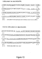
Figure 12 is a schematic block diagram of an exemplary gated window detector for use with the data acquisition system ofFigure 3 to monitor the full bridge power stage circuit ofFigure 2 . -
Figures 13 through 16 illustrate exemplary implementations of registers that may be used to capture overcurrent and overload events for two power amplification channels. -
Figure 17 is a schematic block diagram of an exemplary circuit for detecting overcurrent conditions that occur on a single power amplifier channel. -
Figures 18-21 illustrate various waveforms that may occur in the full-bridge power amplifier channel shown inFigure 2 . -
Figure 21 is a schematic block diagram of an exemplary overvoltage detection circuit that may be used in connection with the data acquisition system ofFigure 3 . -
Figure 1 is a schematic block diagram of anamplifier system 100 that may be used in, for example, a vehicle or the like.System 100 may be constructed as a single or multichannel system. InFigure 1 ,system 100 is shown as a multichannel media system. To this end,system 100 includes a multichannelaudio source 105 that provides multichannel audio to the input of anaudio processor 110. Theaudio processor 110, in turn, provides audio signals for amplification to the input of amultichannel audio amplifier 115. Themultichannel audio amplifier 115 receives power from anamplifier power system 120 that is connected to thepower supply system 125 of the vehicle. Amultichannel speaker system 130 is connected to receive the amplified audio output from themultichannel audio amplifier 115. - The audio amplifier is one example of a power converter. The power converter may control and convert electrical power (such as voltage and current) from one form to another. The following are four example classifications of power conversion: (1) rectification referring to conversion of ac voltage to dc voltage; (2) DC-to-AC conversion; (3) DC-to DC conversion; and (4) AC-to-AC conversion. These four classifications are provided solely for illustration of the applications of a power converter. There may be other classifications of power converters.
- Amplifiers in the audio system may increase the voltage, current, or power of an input signal. One application of an amplifier is in audio equipment. There are several types of classes of amplifiers, such as classes A-D amplifiers. For example, a class D amplifier is a switch mode type of amplifier that may operate in the digital domain. It may employ a pair of transistors that are connected in push-pull and driven to act as a switch, and a series-tuned output filter, which may allow only the fundamental-frequency component of the resultant square wave to reach the load. Moreover, the class D amplifier may generate the equivalent analog output for the speakers in an audio system by using pulse width modulation (PWM) or pulse density modulation (PDM) rather than the traditional digital-to-analog conversion.
- Moreover, it may be difficult to diagnose problems when an amplifier malfunctions. The malfunction may produce a constant error, or may produce an intermittent error (further complicating diagnosis). Class D amplifiers (as well as other some other power converters) may be particularly difficult to diagnose since they operate with a quiescent current. Therefore, it may be especially difficult to diagnose potential problems in a class D amplifier system since currents are normally found even without any output being generated.
- To diagnose potential problems,
system 100 includes adiagnostics system 135 that is adapted to detect and monitor various system signals. For example, various power and modulation signals may be received for analysis by thediagnostics system 135 from themultichannel audio amplifier 115 over one ormore lines 140. Power signals from thevehicle power system 125 may be provided to thediagnostics system 135 over one ormore lines 145. Signals corresponding to the operation of themultichannel speaker system 130 may be provided to thediagnostics system 135 over one ormore lines 150. -
Diagnostics system 135 may include a number of different subsystems adapted to detect and identify various system faults. To this end,diagnostics system 135 may include a multiplexeddata acquisition system 155, one or moreovercurrent detection channels 160; and one or moreovervoltage detection channels 165. Data relating to faults detected bysystem 155 andchannels processor 175. Theprocessor 175 may use the stored information to identify the source of a fault and/or designate action that is to be taken as a result of a fault. For example, the inputs to the diagnostics system may include: the input(s) to the amplifier; the output(s) of the amplifier; the currents in the amplifier system (such as the currents that drive the half bridges of the amplifier); the voltages in the amplifier system (such as the voltages that drive various sections of the amplifier, the voltage of the battery); and sensed temperature in various parts of the amplifier system. Other, or different, inputs may be input to the diagnostic system. - Multichannel
audio amplifier 115 may be constructed in a variety of different manners.Figure 2 is an example of a channelamplifier power stage 200 that may be used in connection withmultichannel power amplifier 115. Thepower stage 200 may be constructed in an integrated circuit format and may be employ a full-bridge switch-mode power stage architecture. The switch-mode power stage 200 may maximize the available load voltage without increasing the peak signal to ground/chassis any more than necessary. EMI may also be reduced by using lower switching potentials as compared to a half-bridge power stage of the same output capabilities. In other examples, however, a half bridge, multiple half and/or full bridges, or any other form of switch mode power stage may be used. -
Figure 2 includes anerror amplifier 202 with an output Verr, and an independent triangle (ramp)generator 204 with an output Tri_out. Theerror amplifier 204 may work in conjunction with a dynamic clamp circuit (not shown), which clamps the error amplifier when the output stage clips. Verr and Tri_out may be sent directly tocomparator 206 which produces differential outputs +PWM(+) and +PWM(-) driving half-bridge 212. Or, Verr and Tri_out may be sent viaintermediate circuitry 218, which may include a -1 gain buffer tocomparator 218, which produces differential outputs -PWM(+) and -PWM(-) driving half-bridge 214. - Any of the currents or voltages in
power stage 200 may be sensed for diagnostic purposes. The current consumption of thepower stage 200 may be sensed and, thus, the power being output by the power stage is correlated to the signals. Specifically, one or both of the differential analog current signals to half-bridges current sensors bridge 212, andcurrent sensors bridge 214. One or both ofcurrent sensors Circuitry 208 may output the greater of the two signals fromcurrent sensors current sensors current sensors Circuitry 210 may output the greater of the two signals fromcurrent sensors current sensors - Further, the PWM signal or signals are available for measurement. For example, one or both of the inputs +PWM(+), +PWM(-) to
half bridge 212 may be sensed, as well as one or both of the inputs - PWM(+), -PWM(-) tohalf bridge 214. Verr, the output oferror amplifier 202 may be sensed and Tri_out, the output oftriangle generator 204 may be sensed. The power supply rail voltages are also available for measurement. The amplified audio channel output is on the +Vout and -Vout terminals. The power stage is powered from +Vcc and -Vcc. -
Figure 3 is a schematic block diagram of an exemplary multiplexeddata acquisition system 155 that can be used as part of thediagnostics system 135 to identify and isolate faults in theamplification system 100.Figures 4 and5 illustrate alternative manners of implementing the write functionality of the acquisition control register 310 shown inFigure 3 , whileFigure 6 illustrates one manner of implementing the read functionality of the various data acquisition system registers 170 of thediagnostics system 135. In other examples, the configuration of thediagnostics system 135 and/or theregisters 170 may be different depending on system design/performance criterion. Thedata acquisition system 155 may be implemented as a CMOS mixed signal integrated circuit. Considerable functionality is possible in CMOS mixed signal ASICs. - The multiplexed
data acquisition system 155 may be employed to digitize scaled versions of various system signals that are to be checked. One or more of the various system signals may be attenuated prior to input to ananalog multiplexer 305. These signals are provided to the input of theanalog multiplexer 305 that is controlled by several output bits of anacquisition control register 310. For example, the output voltage of eachpower amplifier 200 may be monitored using attenuated signals corresponding to signals provided to the speaker leads, +Voutx and -Voutx, where x is the channel number. As shown inFigure 3 , the multiplexer includes input signals for two channels (see +Vout1, - Vout1, +Vout2, -Vout2). Further,Figure 3 illustratesanalog multiplexer 305. However, with additional circuitry,analog multiplexer 305 need not be included. - A scaled or attenuated version of the output stage power supply current may be input to +ISx and -ISx, (such as +IS1 for channel 1) where the currents being monitored are those powering the full bridge output stage. The +ISx and -ISx signals may be derived as single ended versions of the differential +ISx(+) and +ISx(-), and -ISx(+) and -ISx(-), respectively, from the
power stage 200 shown inFigure 2 . - The
analog multiplexer 305 may also input various other signals. For example, various temperature measurements of theaudio amplifier 115 may be input including Tref, which may set a reference for the temperature sensors, Tsensex, which may be used to sense overtemperature using an NTC thermistor. As another example, voltages from theerror amplifier 202, include Verr, may be input to theanalog multiplexer 305. As still another example, +Vcc_trk and -Vcc_trk, representing voltages proportion to the positive and negative supply voltages, respectively, may be input to theanalog multiplexer 305. Finally, Vbat_trk represents a voltage proportional to the battery voltages (such as the voltage from the battery on the vehicle). - The power supply currents of a switch-mode power channel amplifier may contain AC switching signals that correspond to the ripple currents that drive the output demodulation filter. These currents are non-trivial and can comprise 10% or more of the peak current that is allowed at maximum in the stage. Buck-derived output topologies such as class-D half-bridges and full-bridges also have discontinuous power supply current waveforms, making the spectrum of the supply currents very broad. If the unfiltered current waveforms were digitized by the analog-to-digital converter without some form of lowpass filtering, the resulting data output values could span the dynamic range of the fast switching currents of the power supplies. Therefore, a low-
pass filter 315 may be included at the output of themultiplexer 305 to allow filtering of these inputs. The filter may be designed to pass audio frequencies, but to attenuate switching frequencies. - The
data acquisition system 155 may include sample and hold functionality in an analog-to-digital converter 320. Analog-to-digital converter 320 may be constructed as a 10 bit capacitor ladder successive approximation analog to digital converter. Such a 10 bit digital converter has 1024 states or 3 digits of full-scale referenced resolution. - The
data acquisition system 155 may perform an analysis, including a statistical analysis based on the one or more signals input toanalog multiplexer 305. The statistical analysis, discussed in more detail below, may be used to diagnose potential problems in theaudio amplifier 115. Further, the statistical analysis may be performed over a period of one or more cycles or conversions. In this manner, thedata acquisition system 155 may perform the statistical analysis of a large number of data conversions without external processor intervention. - The number of cycles over which to perform the statistical analysis may be variable. For example, burst counter 325 may determine the number of cycles over which to perform the statistical analysis. The
burst counter 325 may have a counter length of 22 bits that facilitates automatic execution of between 1 and 4,194,303 conversions. During the time that these conversions are made, an analysis of the one or more inputs to theanalog multiplexer 305 may be performed. The analysis may be reflected in one or more output registers, which may be used to record the state of one of the signal that is being monitored (such as one of the inputs to the analog multiplexer 305). As shown inFigure 3 , the analysis may include amaximum register 330, which may record the maximum value reached for one of the inputs during the burst cycle. Or, the analysis may include aminimum register 335, which may record the minimum value reached by the monitored signal during the burst cycle. Further, the analysis may include an integrated sum of the monitored signal during the burst to cycle, provided atsum register 340. This integrated sum value may be used by theprocessor 175 to determine the average value for the monitored signal over the burst cycle period. The output of theregisters Figure 7 .Figure 3 illustrates some examples of the analysis on the input signals that may be performed. Other analysis, such as the analysis discussed inFigures 16 and21 , may be performed in addition to (or instead of) the maximum value, minimum value, and sum during a burst period. - To initiate data conversion,
data acquisition register 310 may be written with a non-zero burst count. The input and filter mode may be selected in the same register write operation. The burst count value may be selected to allow a measurement having a burst duration that coincides with the periodicity or record length of some predetermined signal that is being measured, such as a signal that is synthesized by a digital signal processor (DSP) or the like. Or, the burst duration may be determined based on the time analog-to-digital converter 320 takes to covert a signal. Thus, the clock cycle of analog-to-digital converter 320 may be the same as the burst duration. The average value of the signal may have its greatest significance when periodic signals are used and the measuring experiments are designed for the burst to extend over an integer number of signal repetitions. - In
Figure 6 , one or more registers may record the largest number, such as a 10 bit number, that has been seen since the burst measurement began (max), and another (min) records the smallest. These registers are configured to receive the values provided fromregisters Figure 3 . At the start of the burst conversion, themax register 330 and its corresponding counterpart inregister 170 may be set to the smallest value in the number system (in this case zero) and theminimum register 335 and its corresponding counterpart inregister 170 may be set to the largest value in the number system. The resulting max and min of a signal may frequently be a useful statistic and may be gathered automatically insystem 155 by digitally comparing each conversion output with the previously held value. Theregisters register 170, may be updated when a new maximum or minimum is encountered during the burst cycle. - In
Figure 6 , the third register (sum) receives its value fromregisters 340 and corresponds to the accumulated sum of the data that has been digitized since the burst measurement began. If this 32 bit register is read by an external processor that initiated the burst conversion and the 32 bit number is divided by the burst count, the resulting statistic is the average value of the signal being digitized. Since division is an iterative operation, the division may be done byprocessor 175 rather than adding further hardware to thedata acquisition system 155. - In one example, the sum register is read after executing a take a burst of 64 conversions. The value in the sum register at that point is a 16 bit value that corresponds to a 16 bit data conversion. The noise reducing effects of averaging may be evident in the result with a 4x signal-to-noise (S/N) improvement (sqrt(N)). The S/N improvement will occur if the signal being digitized is time varying and/or the measurement contains a least significant bit (LSB) of noise by nature.
- The data acquisition system is very flexible in that traditional single-valued data conversion may still be done if the burst count is set to one. The cost in silicon to implement the added functionality of max, min and sum is very low since modern CMOS processes have small feature size devices used for digital logic.
- The exemplary input data multiplexer shown in
Figure 3 accommodates two power amplification channels that share asingle data converter 320. As discussed above, in addition to supply currents and output voltages being available for digitization, the output of the main feedback loop error amplifiers (Verr) and channel temperature sensor outputs (Tsense) are provided to the input ofmultiplexer 305. The temperature inputs are augmented with an external temperature reference (Tref) that has a voltage level corresponding to the level at which the temperature sensor inputs would be considered to be at their high temperature limit. An autonomous internal system of comparators may use these signals to direct amplifier thermal shutdowns and/or provide warnings and overtemperature status/interrupt signals to the external processor. - Power-Up Diagnostics
- The
system 135 may run an off-line diagnostic upon power-up. A more focused form of testing may be appropriate should a fault be sensed during on-line operation, and a processor interrupt created from the fault. One purpose of the power-up diagnostic may be to discover non-intermittent failures such as short-circuit and open-circuit conditions and to test the functionality of theamplifier system 100 including its power supply. - In one example, there are N channel pairs of PWM amplifiers (2*N channels or 2*N-1 when MaxCh is odd) each pair having an I2C port with a corresponding status register. One manner of implementing the status register is shown at of
Figure 8 . As shown, each channel may have a status bit for overtemperature, temperature warning, overcurrent, high current, clipping, high output voltage, excess overcurrent events and excess clipping events. Excess events may be derived from counting events and/or when a predetermined count is exceeded, a status bit may be set. Clearing the associated counter could be required to clear the status bit. The act of reading the counter may clear the counter. Single event status bits may be cleared by reading the status register unless the condition persists, such as in the case of a thermal condition. -
Figure 9 illustrates a pair of exemplary interruptmask registers processor 175 whileFigure 10 illustrates a pair of corresponding default interruptmask registers programmable registers Figure 9 facilitate program control of the types of events that are to be serviced on a channel-by-channel basis. If need be, the interruptmasks system 100 might be directed to all of the possible causes for an interrupt, whereas testing during normal use might be directed to overtemperature, temperature warning, excess overcurrent events and excess clipping events. If no programmed events are designated, the default register ofFigure 10 may be used. - An example routine that describes a power-up test sequence as could first be done at the factory and perhaps done every time the vehicle is started is included as Appendix A. The thoroughness of the routine is optional in that it can be simplified by doing only certain portions. For example, testing during normal operation may be limited to the initial portions and not loudspeaker testing, which could be reserved for factory and service center testing.
- Pursuant to the test shown in Appendix A, the vehicle battery voltage can be measured by using the Vbat_trk input to the
multiplexer 305. If this voltage is too high, it may not be safe to enable thepower supply 120. If the battery voltage is too low, further discharge of the battery by theamplifier system 100 may be undesirable and enablement of thepower supply 120 may be inhibited. If the battery voltage is within tolerance, thepower supply 120 may be enabled and further diagnostic tests may be continued. - Testing of the initial temperatures Tsense1 and Tsense2 and the temperature reference Tref may then be executed. If they are found to be within a predetermined range, the power up sequence may be continued. A faulty temperature reference Tref may imply a dysfunctional temperature protection system, which is a serious defect. In such instances, the power-up sequence could be aborted.
- The +/-Vcc_trk signals may be used internally in the IC to control the amplitude of PWM modulators. By also making them available to the
data acquisition system 155, it is possible to monitor the power supply voltages used by the output stages of the channel amplifiers to determine if they are within tolerances. This is a basic diagnostic for the power supply which is often regulated and has specific voltage expectations. This test of two measurements could be done before any amplifier channel is enabled. Should thepower supply 120 be out of tolerance, further diagnostic testing could end by disabling thepower supply 120. - Some power supplies allow energy saving modes of operation wherein the power supply voltages can be programmed. All voltage modes could be exercised and compared to acceptable tolerances if a more thorough power supply diagnostic were desired.
- The next set of observations can be made with all amplifier channels disabled and the +/-Vout signals of all channels being measured. If there were twelve channels, then 24 measurements could be made. When the computer interface to the system supports the simultaneous addressing of multiple measuring ICs, they could be gang programmed to make the measurements. An example of such a bus capability appears in the general call address of the I2C bus. In the case of two channeled data acquisition systems being used to test a 12 channel amplifier, then all Vout signals may be measured using only four measurement commands each followed by six fast register reads of the sum registers.
- A channel could require that there be a wait after disabling and before measurement to allow the output filters of the channels to charge their output filters to the rest state. If the output were shorted, that would occur very rapidly. Alternatively, a five time constant wait could be about 75mS.
- If there were a hard fault between the battery and an amplifier output, the same amplifier output could tend to measure similarly to the battery. Channels that are seen to be faulted to battery should not be subsequently enabled. Hard faults to ground could appear at amplifier +/-Vout signals as ground would measure. Since the attenuators for all Vout signals are referenced to a midpoint voltage Vr that may be sourced within the IC, that is the voltage expected when a channel is disabled, not ground. Outputs normally may float up to Vr when not enabled. Outputs may operate near ground when enabled and no input signal is present and may not; at such occasions, be distinguishable from a short. Channels with a fault to ground may be enabled for the purpose of doing a more extensive service diagnostic that would benefit from knowing the fault resistance.
- Internal faults in an amplifier channel amplifier may tend to produce Vout signals that are equivalent to the +/- Vcc_trk signals. This is due to the fact that the most common internal amplifier failures involve faults to a power supply. Under these conditions the channel should not be enabled. It may be possible to continue the testing of and operation of all other channels that were not found faulted. Further testing of faulted channels may have diagnostic purpose depending on the nature of the fault. Faults to Vcc would not necessarily be such an occasion.
- Once the basic integrity of the system has been observed with the
amplifier channels 115 disabled, it is possible to advance to testing with theamplifier channels 115 enabled one by one. Comparing Verr signals to +/-Vout signals is one manner of testing the basic DC functionality of a channel. If any of the three signals has an unexpected DC offset, the channel may be defective. The average value of the supply currents could have a tolerance which could be observed at this time. - If only one channel is enabled at a time it is possible to test for hard faults between channels. The Vout signals of the enabled channel could be expected to go to ground while all others could remain at Vr. Any Vout line of a disabled amplifier that goes to ground may be identified as having a hard short to one of the two now driven Vout signals. Channels that are seen to be faulted together should not be subsequently enabled except for the cause of doing a service diagnostic that would benefit from an analysis of the cross-connecting resistance. In practice, faults between channels are most likely when they share segments of a wiring harness or are adjacent in a connector. Gang programming during channel-to-channel fault tests would be possible if associated pairs were enabled in separate groups.
- Once the channels are observed to be properly functioning with no faults to any external or internal circuits speaker tests may be performed. Speaker shorts and opens may be tested with the introduction of input signals (from a DSP) to fully enabled amplifier channels. With a two channel data acquisition system (as shown in
Figure 3 ), only two test periods would be needed for a 12 channel amplifier as groups of six could be done in unison assuming the amplifier power supply permits the demand. Channels having multi-way crossovers could need to be given as many tests as there are transducer frequency bands. - Each speaker has an expected range of impedance for any given frequency of stimulus and thus has an expected current draw from the power stage for any given stimulus. The low pass filtered supply currents may be measured to minimize the inclusion of switching frequency content. Multi-way channels that have passive crossovers may be tested by using signals that are in-band for each loudspeaker, and be as much out-of-band as possible for the other speakers.
- The multi-way case is the testing of tweeters where the test can be done with, for example, 21KHz bursts. A burst of a few cycles, for example <500uS, may be all that is needed for each test group. Even when the tweeter is open, the mid-range can draw some current, but less than would be expected if the tweeter were present. The ability to resolve the tweeter's current within the total channel current is important to this test. Use of a 10 bit conversion of the +/-IS signals could suffice. The
maximum register 330 could be all that is needed in the observation using a simple high/low pass/fail criterion. If the current is to high, there may be a fault somewhere in the system, either lead-to-lead or within the transducer. If the current is too low, the transducer may be open or defective. - Transducers that are directly connected can be tested with a low-frequency stimulus that is below audibility or far below acoustic transduction limits for the transducer. A signal such as a synchronization pulse may be used to minimize unintended bandwidth and excess power while still allowing a large peak signal thereby providing a good S/N ratio with respect to the current information.
- A subsonic pulse that could last for a predetermined time, such as only 200mS, may be used to facilitate testing of the 12 channel example. In this manner, the low-frequency response may be tested' in <300mS using the gang programming of six two-channel ICs included in the
system 100. One reason testing may be accomplished in less than twice the stimulus test time is that it is not necessary to wait for the full extent of one test group to finish before the next group is started. This is because the peak current draw would be expected at ~100mS into each test and the two tests could overlap with data acquisition finishing at approximately 110mS into each signal. More extensive diagnostics can be done for a number of cases that have been identified as defects in off-line diagnostics. - It may be desirable for an audio amplifier such as used in a vehicle to be able to perform fault diagnostics in real-time with a minimum of special tests and diagnostic software usage. No signals other than those of normal usage, music and speech, may be used as the test stimuli. Complicating the matter is that the faults that are common are often intermittent in nature due to the high vibration present in the vehicle environment. Faults that are non-intermittent are usually much simpler to diagnose.
- Insulating materials are at risk in vehicle environments due to extremes of temperature, chemical assaults and abrasion driven by shock and vibration. The output leads of a multichannel audio amplifier are at risk of four primary types of fault:
- 1. Short to ground/chassis
- 2. Short to battery potential
- 3. Short across the speaker leads
- 4. Short to another channel's speaker leads
- Short to ground is the most likely due to the prevalence of the vehicles chassis. Sharp edges on sheet metal and pinches are a frequent cause of insulation failure which is also aggravated by vibration. Shorts to battery can occur within the wiring harness when wire to wire insulation fails or connectors become damaged. Not all battery circuits are continuously powered, i.e. turn signals, door locks, window motors, etc. Shorts across the speaker leads can happen anywhere along their path but within the loudspeaker is a very likely location due to proximity and possible high temperature operation of voice coils. The short to another channel's speaker leads is the least likely fault and is most likely to happen in or near the amplifier. As the wiring harness fans out from the amplifier such encounters are less likely.
- Each fault may be constructed of multiple impedances in series which can become the effective load to an amplifier channel. Every one of the primary types includes the speaker lead impedance, a fault-point connection and a return path impedance. The fault-point connection portion of the total impedance may be very erratic and less than ideal as a short. Contact areas may be small and arcs may be initiated within the contact area. When arcs occur, the connecting plasma may become unstable and the vapor pressure of ionized metal may attempt to extinguish (blow out) the connection. The high temperature of the plasma may alter the surface texture of the adjacent metal, which then alters the electric field structure that triggers temporarily disconnecting plasmas to rejoin. Any energy lost to the resistance of the plasma may act to heat it further. Inductance in the surrounding circuit can enable transients of voltage that can re-fire the circuit making disconnection less likely. An arc is a random process even when it is sourced by a highly resonant structure.
- The impedance of a speaker lead is the best understood part of the circuit but may not be a low inductance resistance. The self inductance of the speaker lead is an active part of the circuit.
- The return impedance may vary greatly with the type of fault incurred. Faults to chassis are most likely to have a low impedance return path. Faults to another lead in a harness may be of similar character to the speaker lead portion. Battery circuits may contain unusual transient loads and even signal sources.
- In many instances, power channel amplifiers can be powered from voltages greater than the battery potential of the vehicle power supply. Such amplifiers also may not employ ground as one of the output stage supply potentials, instead using a negative supply (-Vcc) similar in voltage magnitude to the positive supply (+Vcc).
- When a power channel amplifier is a source with potentials greater than either ground or battery potential, fault currents may flow in both directions from the power channel amplifier. Therefore, the impedances within the fault circuit can give rise to both steady-state and transient potentials that, on the power channel amplifier end, differ significantly from ground or battery in either polarity or difference.
- Significant faults may result in currents large enough that protective circuitry within the amplifier will be forced to operate to prevent amplifier destruction. One means available to the amplifier to understand the nature of the fault that it senses is to examine the output voltage at the time of overload. If the voltage of the amplifier outputs are examined at the moments of current overload for any given channel, there can be increased probability that the amplifier potential is within a range of voltage above or below the potential of ground or battery. The bimodal distribution of overload voltages could peak near (+/-lpk*E[Rckt]) about ground or battery where lpk is the limiting value of amplifier current and E[Rckt] is the statistically expected value of the fault circuit resistance. The L*dl/dt portion of the signal may spread the distribution of the fault voltage as the erratic nature of any arc results in a lively random dl/dt term.
- When using a switch-mode amplifier, the demodulation filter is resonant and may introduce large transients of voltage when intermittent shorts are encountered. The transients may resonate at the dominant mode frequency of the filter. Voltages of 3 times the magnitude of Vcc are sometimes seen during intermittent faults. The dynamic nature of the voltage at the time of the current overload may prevent a highly accurate determination of the type of a fault based upon a single observation. Accurate fault detection may, however, be performed statistically.
- When using a compact set of tests and measuring hardware, one method is to capture the statistics of the events, such as counting the number of overload events that occur when the output voltage of the suspect output is within a window of potential that spans the aforementioned bimodal distribution of voltages about ground and battery potential.
- One method may include using gated window detectors that observe the output voltages and comparing them to a window of voltages that represent ground or battery. These window detectors may be gated by current overload events from the same channel of either polarity of supply. The output of the window detectors may be counted using a counter that increments with each event. Sixteen bits or more of a roll-over-inhibited binary counter can be used. The fact that such comparators are not active until an overload is already sensed, minimizes any risk that these detectors will create noise that disturbs proper signal processing, or creates EMI.
- A full-bridge channel such as the one shown in
Figure 2 may have four gated window detectors, two on each output signal voltage. Of these two, one could be making comparison to a range of voltages about ground and the other to a range of voltages about battery potential. A two channel IC supporting such a paradigm may contain eight window detectors each with its own counter. Each channel may also include counters that count current overloads in each Vcc. - To diagnose a fault,
processor 175 may first observe the overcurrent status of thestatus register 800 for the channel. Once theprocessor 175 determines that an overload is reported in a channel(s), a command may be given by theprocessor 175 to freeze the counting activity in all related counters for the channel(s) under investigation. All counters may be read before clearing the freeze bit. If the counts are not significant/too small, the diagnosis may be deferred until more counts have been gathered. - If more than one channel is reporting overloads, one explanation is that they are intermittently shorted together. Since any voltage is possible in this scenario it is not too useful to note what the counts from battery and ground counters were. (fault type 4) If the number of counts in an output windowing ground significantly exceeds the number of counts windowing battery, then output may be being shorted to ground (or vice versa) (
fault types 1 or 2). If the number of overloads is large and neither windowing detector has an appropriate bias, then a shorted speaker may be likely (fault type 3). - To accommodate the range of impedances found in a variety of vehicle models, it may be necessary to adjust the window dimensions on a per channel basis for both battery and ground. The wiring resistances and return impedances may be different for each channel. The addition of accessories on battery circuits could also bias the proper window to lower voltages for maximized detection of faults to the battery. Since it is unlikely that the two outputs of a given channel are different in a given vehicle model, both output voltages could test by using the same windows. Alternatively, the windows could be specific for each output signal of a full-bridge output stage.
- Some improvement in information may be possible if the windows are split into positive and negative halves with positive current overloads enabling window detectors using positive window halves, and negative current overloads having their own window detectors utilizing the negative window halves. One reason that this doubling of hardware may give some improvement in accuracy stems from the positive real nature of the impedances. Doubling the quantity of window detectors again to include positive overcurrents enabling the window detectors from negative window halves and vice versa may be used to improve diagnosis of channel-to-channel shorts. It is unlikely that any such improvement is advantageous as channel-to-channel shorts tend to be obvious from the fact that two channels are both encountering overload.
-
Figure 11 is a schematic diagram of one example of a statisticalfault sensor circuit 1100 that may be used for a windowing system that may be used in connection with a single detection channel. As shown,circuit 1100 employs a plurality ofgated window detectors 1105. Ground potential can be measured as the equivalent voltage is not synonymous with actual ground voltage. Since the external attenuator formed from resistors R1 and R2 is design specific, the Vgnd attenuator may not be internal to the IC. - As shown in
Figure 11 , thewindow detectors 1105 may be triggered by an overcurrent signal (OC). The overcurrent signal (OC) may be generated as shown inFigure 16 . In this manner, at the time an overcurrent occurs, various signals may be analyzed, such as counting the number of times certain events occur. For example, the 16 bit counters for +Voutx_Vbat or -Voutx_Vbat may count the number of times that one of the output voltages +Voutx and -Voutx is the same as Vbat. Similarly, the 16 bit counters for +Voutx_Vgnd or -Voutx_Vgnd may count the number of times that one of the output voltages +Voutx and -Voutx is the same as Vgnd. This may be used to analyze whether one of the output channels is shorted to Vbat or Vgnd. Similarly, other voltages may be compared to Vbat or Vgnd (or other voltages) and may be subject to similar counts when an overcurrent (OC) occurs. -
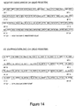
Figure 12 is a schematic diagram of one example of agated window detector 1105 that may be used in the statisticalfault sensor circuit 1100. In this example, the signal range of the output voltage ports to thewindow detector 1105 may be within the bounds of Vdd and ground. The window potentials may be bounded by nature since the attenuator ratios can be substantially identical for all attenuators. Vbat may have a transient component that results in clamping on the gate protection networks. As long as there are no errors other than saturation in this input, the transient component may be of no serious concern. In general, the operating range of thedetector 1105 may be between the window potentials, well within the bounds of Vdd and ground. - The window half voltages produced across the resistors R1 and R2 shown in
Figure 11 may be approximately 20% of Vdd, such as 1V at full scale. The three bit digital-to-analog converters (DACs) that may linearly program this voltage may step from 1 to 8 units of current by gating three current sources that are symmetrically mirrored to form both upper and lower halves of the window. A fourth current source may provide one unit (LSB) of ungated current. - Intermittent faults can be diagnosed on the first level by using data that has been accumulated by counting overcurrent and overload events.
Figures 13 through 16 illustrate exemplary implementations of registers that may be used to capture overcurrent and overload events for two channels. Since the output stage may provide current information that is power supply specific, it is possible to count the overload events associated with each supply. -
Figure 17 is a schematic block diagram of anexemplary circuit 1700 for detecting overcurrent conditions that occur on a single power amplifier channel.Circuit 1700 may be used to implement theovercurrent detection channels 160 shown inFigure 1 . The output registers ofcircuit 1700 may be provided to registers arranged in a manner shown inFigures 13 through 16 , which may be part of thesystem register storage 170 shown inFigure 1 . - As shown in
Figure 17 , the current signal outputs of the full-bridge power stage +IS(+), +IS(-) and -IS(+), -IS(-) (shown inFigure 2 ) may be received bydifferential receivers comparators Figure 17 , +IS, -IS are compared with V11 and V12. V11 may represent a voltage at which an overload condition may occur. V12 may represent a voltage less than V11, but than may represent a voltage higher than expected for the normal operation ofaudio amplifier 115. If either +IS, -IS voltage level exceeds voltage VI1, the signal limit goes to an active state and the corresponding power amplifier channel may be inhibited from further operation. In one example, Ilimit is the OR of the overcurrent signals produced from both supplies. Any assertion of the Ilimit signal to an active state may set a latch, such as S/R flip-flop 1735, which represent the overcurrent signal (OC) and may be used to initiate an interrupt to theprocessor 175 if so desired. In addition, other comparisons may be performed that analyze higher than normal current (but not an overcurrent) in the circuit. For example, as described above, V12 may less than the value of V11, such as 80% of the value of V11. If either +IS, -IS voltage level exceeds voltage V12, a latch, such as S/R flip-flop 1760, may be set indicating a high current status. The high current status may be used as an interrupt toprocessor 175, indicating a potential problem in theaudio amplifier 115. - The number of Ilimit events (including both negative and positive overcurrents) may be counted using an
overcurrent counter 1740. The number of Ilimit events for negative overcurrents may be counted using anovercurrent counter 1750, and the number of Ilimit events for positive overcurrents may be counted using anovercurrent counter 1755. - The
overcurrent counter 1740 may be tapped at point Qt. If the Qt count is ever reached, it may set a status latch, such as S/R flip-flop 1745, to indicate that an excessive number of overcurrent events have occurred. To this end, the setting oflatch 1745 may be used to initiate an interrupt to indicate the occurrence of an excess number of overcurrent events to theprocessor 175. The value for Qt may be programmed or fixed. By setting the value for Qt to count a significant number of overcurrent events, it is possible to minimize the tendency to report systems as defective that have only encountered a single static glitch or a minor number of non-recurring errors. The reporting of false positives may be a major cause of annoyance to vehicle owners and may create needless service costs. When a fault is genuine, the rate of counting may be very high, often at the switching frequency of the output stage. This further improves the discrimination between actual faults and glitches in the system. - The system shown in
Figure 17 employs 32 bit counters and the switching frequency of the input signals may be about 250KHz. When the counter saturates, it may cease further counting rather than allowing a roll-over error. With multiple overcurrent counters, such as positivesupply overcurrent counter 1755, negativesupply overcurrent counter 1750, and thetotal overcurrent counter 1740, as illustrated in the register configuration ofFigures 13-16 , it is possible to improve the accuracy of fault detection and to identify the source of the faults. - When a fault develops between a speaker lead and the vehicle chassis or ground, large magnitude signals may encounter overcurrent limiting whenever the voltage across the fault divided by the fault resistance reaches the current limit value. If the fault resistance is large, then the overcurrent events will be rare. Likewise if the signal level is low, the overcurrent events will be rare. Whenever the signals are large enough to produce overcurrent events, the positive and negative events can occur in time alternation which results in the
overcurrent counter 1740 being equal in count to the sum of the positive andnegative overcurrent counters negative counters overcurrent counter number 1740 will be in each of the polaritysensitive counters - On the other hand, assume that a fault develops between a speaker lead and the battery. In this situation, it is more likely to have overcurrent events in the negative supply as compared to the positive supply. This is because the battery voltage adds to the difference potential between the speaker lead and the supply potential of the negative switch, whereas it diminishes the potential between the speaker lead and the supply potential of the positive switch. The
main overcurrent counter 1740 is still likely to accumulate these counts in time alternation making the most probable value for that counter exactly equal to the sum of the positive andnegative overcurrent counters - If a fault develops between speaker leads it is possible to have overcurrent simultaneously in both polarities of overcurrent. The more sensitive of the two limit currents will tend to dominate the individual polarity sensitive counters, but the lack of strict time alternation between counts can now result in the OR-ed count of
register 1740 being less than the sum of the positive andnegative overcurrent counters - Channel-to-channel speaker lead faults may be readily identified as there may be overcurrent events recorded in the counters of more than one channel. Since overcurrent should be rare by design, to have multiple channels with overcurrent events can mean primarily one thing, i.e. the channels are inadvertently joined with one another. In this case, overcurrent events tend to be in time alternation and positive overcurrent events are as likely as negative overcurrent events.
- In one example system, an I2C bus interface may read the overcurrent counters and poll the status register(s) that contain the status bits described in connection with
Figure 17 . The act of reading the counters or the status register(s) may act to automatically clear the interrogated counter or status register. Any of the status bits can be mapped to one of two interrupt pins as programmed by interrupt mapping registers. - Power supply currents to class-AB amplifiers at large output currents are simple rectified versions of the load current and can be easily monitored for magnitudes of load current. As long as the current being compared is well above the quiescent bias current levels of the class-AB aspects of the design, monitoring load current using supply currents is straight-forward.
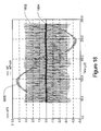
- Switch-mode power stages circulate substantial currents in inductances that are used at the input to the output filter. These inductances receive the PWM switching waveforms of the power stage and create continuous currents that within the inductors ripple about the output load current with waveforms that are triangular in form. These same currents are switched between the power supply rails creating supply currents that are discontinuous. An example of the supply current to a full-bridge that is switching at 250KHz with interleaved modulation at 5KHz is shown in the waveforms of
Figures 18 - 21 .Figure 19 is an exploded view of the waveforms shown inFigure 18 to provide better view of the currents. In like mannerFigure 21 is an exploded view of the waveforms shown inFigure 20 . - In
Figure 18 , the >3Apkcurrent waveform 1802 is very large compared to the 20KHz low-passfiltered supply current 1804. The actual load current is just over 1Apk, but because the class-D power stage functions as a power converter, the actual peak load induced supply current is attenuated by the ratio of the output voltage divided by the supply voltage which in this case is 4.3/52. - The filtered output voltage is the
sinusoidal waveform 1806. The waveform shows some small amount of distortion since this power converter is operating.open loop in this test. The ripple on the sine wave is the part of the large 52Vpk switching waveform that is not fully filtered in the output. As shown inFigure 18 , near zero, the ripple is very small as this is an interleaved full-bridge converter. InFigures 18 and19 , the waveform is modulating with a 0.1 modulation index, i.e. 20dB below maximum level. InFigures 20 and21 , the waveform is operating with a 0.9 modulation index, i.e. 0.9dB below maximum level. - The output voltage is now 41Vpk resulting in a supply current attenuation factor of 41/52 and a clearly visible current signal when low-pass filtered by the 20KHz low-pass filter. Were it not for the 20KHz filter, the
current waveform 1802 would be much more difficult to observe. A 41Vpk corresponds to 210W average power into a 4 Ohm load which is what is shown in this case. Exactly one cycle of 5KHz is shown. The ripple on the peaks of theoutput voltage waveform 1806 is diminished from what is seen at 26V levels. This is the function of an interleave of two converter which has nulls in the output ripple at zero signal and peak signal. The power supply current waveforms of a switch-mode converter are filtered to allow judgments about load current. The output signal should be of substantial level so as to create substantial supply currents. This differs from the class-AB case. As such, a data acquisition system that provides data about load current from such signals may include a low-pass filter that has substantial attenuation at the switching frequency. The statistical diagnostics approach taken to counting overcurrent events can also be extended to counting all overload events which now adds the dimension of overvoltage (clipping) detection to the diagnostics hardware. -
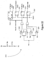
Figure 22 is a schematic diagram of one example of anovervoltage detection circuit 2200 including its corresponding registers.Circuit 2200 may be used to implement theovervoltage detection channels 165 shown inFigure 1 . Incircuit 2200,window comparators window comparators triangle generator 204 for amplitude control. Vtp and Vtn track the power supply voltages to the power output stage of the power amplifier channel. This method results in constant stage gain by using feed-forward control of the modulation. Any time that the error signal Verr goes beyond these limits, the modulator of the power amplifier channel is saturated and is in overload. This results in the setting of a status bit using, for example, S/R flip-flop 2215. - Actual overloads are counted in a
clipping counter 2220. Any overload of major duration may be captured in this counter. Clipping conditions will result in errors within the amplifier feedback loop and can result in counting. The counting rate ofcounter 2220 may be well below the switching rate of the power amplifier channel since the error amplifier does not generally sense every switching event as an individual error. Rather, errors may extend over whole switching cycles. As such, theclipping counter 2220 may give another statistical perspective to the fault problem. Theclipping counter 2220 may count the number of audio frequency clipping events rather than the number of switching cycles that were' involved. When theclipping counter 2220 counts to a tap point Qt on the clipping counter, a status bit may be set using, for example, S/R flip-flop 2225. Tap point Qt of clippingcounter 2220 need not be equal in value to the tap point Qt on theovercurrent counter 1740 ofovercurrent detection circuit 1700. Since theclipping counter 2220 tends to count more slowly, it would not be useful if the two tap points were the same. In like manner to theexcess count register 1740 of theovercurrent detection circuit 1700, theexcess clipping counter 2225 may be used to interrupt theprocessor 175. - Having a high number of clip events in a properly programmed system should rarely occur. The output of the
audio processor 110 should be maintained to keep the peak signal voltage beneath the available supply voltage unless the user is pushing thesystem 100 for all it can do at high level. Since theprocessor 175 is programmed to know the intended operating level and also may be in control of the amplifier power supply potentials, it can interpret whether the value counted by theclipping counter 2220 is proper for the operating conditions. Having a large number of clipping events with no apparent cause may be a symptom of a defective power amplifier channel. The implication is that the loop feedback is no longer in control of the power amplifier channel and the channel may need to be taken out of service with an unknown defect. - A second set of
window comparator R flip flop 2240. Additionally, signals that exceed the predefined window of Vtp and Vtn may be used to set the clipping status register 2215. The signal from the highvoltage status latch 2240 is not an overload condition identifier. Rather, the inference of the use of this feature is that the level of the error signal Verr is larger than normally expected. - An interrupt system may be used while the
system 100 is in use to detect faults as they appear. In one example, there may be N channel pairs of PWM amplifiers (2*N channels or 2*N-1 when MaxCh is odd) each pair having an I2C port with a status register. Each channel may have a status bit for overtemperature, temperature warning, overcurrent, high current, clipping, high output voltage, excess overcurrent events and excess clipping events. Excess events may be derived from counting events and when a predetermined count is exceeded, a status bit may be set. Clearing the associated counter could be required to clear the status bit. The act of reading the counter may clear the counter. Single event status bits may be cleared by reading the status register unless the condition persists, i.e. thermal. - An internal interrupt mask register may be used to associate each of the status bit with interrupt generation. (See
Figures 9 and10 ). This allows program control of what types of events are serviced on a channel-by-channel basis. If need be, the interrupt mask can be redefined dynamically. For example, the factory testing of thesystem 100 might be set to detect all of the possible causes for an interrupt whereas subsequent normal use, such as field use of thesystem 100, may be programmed to simply detect overtemperature, temperature warning, excess overcurrent events, and excess clipping events. An exemplary interrupt event service routine is shown in Appendix B. Further refinement in identifying the nature of intermittent faults is possible by using information derived from cross-correlating overcurrent events, clipping events, and instantaneous output voltage measurements. - While various embodiments of the invention have been described, it will be apparent to those of ordinary skill in the art that many more embodiments and implementations are possible within the scope of the invention. Accordingly, the invention is not to be restricted except in light of the attached claims.
-
 Begin Power-Up Diagnostic;
 ; Make sure we are starting with nothing on
 Disable power supply to amplifier
 Place all channels in standby (gang program w general call addr GCA)
 Initialize all interrupt masks to disable interrupts GCA
 Mute audio signals at DSP
 ;Test that supplies are safe
 Measure Vbat_trk & compare to legal limits
 If Vbat in tolerance
 ;Use max voltage for test purposes
 Enable power supply to amplifier at max voltage
 Wait for supply to come up (Tps=??)
 Measure +Vcc_trk & compare to legal limits
 If +Vcc_trk is out of tolerance
 ;power supply is defective, go no further
 Log error
 Report error to operator?
 Return
 End
 Measure -Vcc_trk & compare to legal limits
 If -Vcc_trk is out of tolerance
 ; power supply is defective, go no further
 Log error
 Report error to operator?
 Return
 End
 Else
 ; battery voltage wrong, go no further
 Log error
 Report error to operator?
 Return
 End
 Wait (∼75mS-Tps) for output filters to settle
 DoWhile waiting
 ; Verify temp reporting system and Data Acquisition System sanity
 ; gather burst of 64 measurements for accuracy's sake & use LP filt
 Send measure Tref(LP64) command to all acquisition registers GCA
 Wait for measurement to complete (∼600uS at 125K meas/sec)
 For Dev = 1 to N
 Read Tref value from Dev sum register
 If Tref_val is out of tolerance
 ; bad temp reference or DAS
 Log error
 Flag Ch1 of unit Dev to remain in standby
 Flag Ch2 of unit Dev to remain in standby
 Report error to operator?
 End
 End
 ; gather burst of 64 measurements for accuracy's sake
 Send measure Tsense1 (LP64) command to all acquisition registers GCA
 Wait for measurement to complete (∼600uS at 125K meas/sec)
 For Dev = 1 to N
 Read Tsense1 value from Dev sum register
 If Tsense1_val is too hot (small)
 ; could happen but not too often
 Log error
 Increase cooling?
 If more than TBD occurrences
 Report error to operator?
 End
 Flag channel(s) associated with Tsense1 to remain in standby
 Else
 Check to see if channel(s) were in standby for being too hot
 If yes and too hot was only reason
 Clear standby flags of channel(s) associated w Tsense1
 End
 End
 End
 Send measure Tsense2(LP64) command to all acquisition registers GCA
 Wait for measurement to complete (∼600uS at 125K meas/sec)
 For Dev = 1 to N
 Read Tsense2 value from Dev sum register
 If Tsense2_val is too hot (small)
 ; could happen but not too often
 Log error
 Increase cooling?
 If more than TBD occurrences
 Report error to operator?
 End
 Flag channel(s) associated with Tsense2 to remain in standby
 Else
 Check to see if channel(s) were in standby for being too hot
 If yes and too hot was only reason
 Clear standby flags of channel(s) associated w Tsense2
 End
 End
 End
 ; Sanity test on error amplifiers
 ; Look to see that all Verr signals are clamped near zero signal
 Send measure Verr1 (LP64) command to all acquisition registers GCA
 Wait for measurement to complete (∼600uS at 125K meas/sec)
 For Dev = 1 to N
 Read Verr1 value from Dev sum register
 If Verr1_val is out of tolerance
 Log error
 Flag Ch1 of unit Dev to remain in standby
 Report error to operator?
 End
 End
 Send measure Verr2(LP64) command to all acquisition registers GCA
 Wait for measurement to complete (∼600uS at 125K meas/sec)
 For Dev = 1 to N
 Read Verr2 value from Dev sum register
 If Verr2_val is out of tolerance
 Log error
 Flag Ch2 of unit Dev to remain in standby
 Report error to operator?
 End
 End
 ; Clear all counters by reading them.. should be zero but be sure
 For Dev = 1 to N
 ; Could be one block read
 Read Ch1 Overcurrent event counter of unit Dev
 Read Ch1 +Overcurrent event counter of unit Dev
 Read Ch1 -Overcurrent event counter of unit Dev
 Read Ch1 Overload event counter of unit Dev
 Read Ch2 Overcurrent event counter of unit Dev
 Read Ch2 +Overcurrent event counter of unit Dev
 Read Ch2 -Overcurrent event counter of unit Dev
 Read Ch2 Overload event counter of unit Dev
 ; Clear all status bits
 Read status register of unit Dev
 End
 End DoWhile
 ; measure all Vouts to check for stuck-at faults
 Send measure +Vout1 (64) command to all acquisition registers GCA
 Wait for measurement to complete (∼550uS at 125K meas/sec)
 For Dev = 1 to N
 Read +Vout1 value from sum register of unit Dev
 ; Proper voltage is mid-point of IC voltage
 ; Test for hostile stuck at supply faults
 If +Vout1_val approx Vbat_trk, +Vcc_trk or -Vcc_trk
 Log error
 Flag Ch1 of unit Dev to remain in standby
 Report error to operator?
 ; Check for short to ground
 Elself +Vout1_val approx Vgrnd
 Log error
 Flag Ch1 of unit Dev to remain in standby
 Report error to operator?
 ; Check for some strange voltage/leakage in output stage
 Elself +Vout1_val not approx Vr
 Log error
 Flag Ch1 of unit Dev to remain in standby
 Report error to operator?
 End
 End
 ; Should be a repeat of test of +Vout1 as should be equal
 Send measure -Vout1 (64) command to all acquisition registers GCA
 Wait for measurement to complete (∼550uS at 125K meas/sec)
 For Dev = 1 to N
 Read -Vout1 value from sum register of unit Dev
 ; Proper voltage is mid-point of IC voltage
 ; Test for hostile stuck at supply faults
 If -Vout1_val approx Vbat_trk, +Vcc_trk or -Vcc_trk
 Log error
 Flag Ch1 of unit Dev to remain in standby
 Report error to operator?
 ; Check for short to ground
 Elself -Vout1_val approx Vgrnd
 Log error
 Flag Ch1 of unit Dev to remain in standby
 Report error to operator?
 ; Check for some strange voltage/leakage in output stage
 Elself -Vout1_val not approx Vr
 Log error
 Flag Ch1 of unit Dev to remain in standby
 Report error to operator?
 End
 End
 Send measure +Vout2(64) command to all acquisition registers GCA
 Wait for measurement to complete (~550uS at 125K meas/sec)
 For Dev = 1 to N
 If ((Dev = N) AND (MaxCh is odd)) Break
 Read +Vout2 value from sum register of unit Dev
 ; Proper voltage is mid-point of IC voltage
 ; Test for hostile stuck at supply faults
 If +Vout2_val approx Vbat_trk, +Vcc_trk or -Vcc_trk
 Log error
 Flag Ch2 of unit Dev to remain in standby
 Report error to operator?
 ; Check for short to ground
 Elsetlf +Vout2_val approx Vgrnd
 Log error
 Flag Ch2 of unit Dev to remain in standby
 Report error to operator?
 ; Check for some strange voltage/leakage in output stage
 Elself +Vout2_val not approx Vr
 Log error
 Flag Ch2 of unit Dev to remain in standby
 Report error to operator?
 End
 End
 ; Should be a repeat of test of +Vout1 as should be equal
 Send measure -Vout2(64) command to all acquisition registers GCA
 Wait for measurement to complete (~550uS at 125K meas/sec)
 For Dev = 1 to N
 If ((Dev = N) AND (MaxCh is odd)) Break
 Read -Vout2 value from sum register of unit Dev
 ; Proper voltage is mid-point of IC voltage
 ; Test for hostile stuck at supply faults
 If -Vout2_val approx Vbat_trk, +Vcc_trk or -Vcc_trk
 Log error
 Flag Ch2 of unit Dev to remain in standby
 Report error to operator?
 ; Check for short to ground
 Elself -Vout2_val approx Vgrnd
 Log error
 Flag Ch2 of unit Dev to remain in standby
 Report error to operator?
 ; Check for some strange voltage/leakage in output stage
 Elself -Vout2_val not approx Vr
 Log error
 Flag Ch2 of unit Dev to remain in standby
 Report error to operator?
 End
 End
 ; Enable the amplifiers one channel at a time and check for errors
 Initialize interrupt masks for interrupt on single overcurrent GCA
 For Dev = 1 to N
 If Ch1 of unit Dev is eligible to run
 Enable Ch1 of unit Dev
 Wait 50uS
 ; Use LP filter to eliminate switching noise
 Measure Verr1 (LP64) of unit Dev
 Wait for measurement to complete (~600uS at 125K meas/sec)
 ; Is error amp fully in control
 If Verr1_val is out of tolerance of Vr
 Log error
 Flag Ch1 of unit Dev to remain in standby
 Disable Ch1 of unit Dev (standby)
 Report error to operator?
 End
 Measure +Vout1(LP64) of unit Dev
 Wait for measurement to complete (~600uS at 125K meas/sec)
 ; Vouts go to - Vgnd when running
 If +Vout1_val is out of tolerance of Vgnd
 Log error
 Flag Ch1 of unit Dev to remain in standby
 Disable Ch1 of unit Dev (standby)
 Report error to operator?
 End
 Send measure -Vout1(LP64) command to acquisition registers GCA
 Wait for measurement to complete (~600uS at 125K meas/sec)
 ; Check tor DC on speaKer
 If +Vout1_val- -Vout1_val not -zero
 Log error
 Flag Ch1 of unit Dev to remain in standby
 Disable Ch1 of unit Dev (standby)
 Report error to operator?
 End
 ; Check for short to other channels if any
 For Dev2 = Dev+1 to N
 ; data has been gathered already for other Ch1s
 Read -Vout1 of unit Dev2
 If -Vout1_val2 -= -Vout1_val
 Log error
 Flag Ch1 of unit Dev to remain in standby
 Flag Ch1 of unit Dev2 to remain in standby
 Report error to operator?
 End
 End
 If ((Dev = N) AND (MaxCh is odd)) Break
 ; Look for faults to Ch2s
 Send measure -Vout2(LP64) command to acquisition registers GCA
 Wait for measurement to complete (∼600uS at 125K meas/sec)
 Read -Vout2 of unit Dev
 If -Vout2_val -= -Vout1_val
 Log error
 Flag Ch1 of unit Dev to remain in standby
 Flag Ch2 of unit Dev to remain in standby
 Report error to operator?
 End
 ; proceed to other Ch2s
 For Dev2 = Dev+1 to N
 If ((Dev2 = N) AND (MaxCh is odd)) Break
 Read -Vout2 of unit Dev2
 If -Vout2_val2 ∼= -Vout2_val
 Log error
 Flag Ch1 of unit Dev to remain in standby
 Flag Ch2 of unit Dev2 to remain in standby
 Report error to operator
 End
 End
 End
 If Ch2 of unit Dev is eligible to run
 Enable Ch2 of unit Dev
 Wait 50uS
 ; Use LP filter to eliminate switching noise
 Measure Verr2(LP64) of unit Dev
 Wait for measurement to complete (~600uS at 125K meas/sec)
 ; Is error amp fully in control
 If Verr2_val is out of tolerance of Vr
 Log error
 Flag Ch2 of unit Dev to remain in standby
 Disable Ch2 of unit Dev (standby)
 Report error to operator?
 End
 Measure +Vout2(LP64) of unit Dev
 Wait for measurement to complete (~600uS at 125K meas/sec)
 ; Vouts go to - Vgnd when running
 If +Vout2_val is out of tolerance of Vgnd
 Log error
 Flag Ch2 of unit Dev to remain in standby
 Disable Ch2 of unit Dev (standby)
 Report error to operator?
 End
 Send measure -Vout2(LP64) command to acquisition registers GCA
 Wait for measurement to complete (~600uS at 125K meas/sec)
 ; Check for DC on speaker
 If +Vout2_val - -Vout2_val not -zero
 Log error
 Flag Ch2 of unit Dev to remain in standby
 Disable Ch2 of unit Dev (standby)
 Report error to operator?
 End
 ; Check for short to other channels if any
 For Dev2 = Dev+1 to N'
 ; data has been gathered already for other Ch2s
 Read -Vout2 of unit Dev2
 If -Vout2_val2 -= -Vout2_val
 Log error
 Flag Ch2 of unit Dev to remain in standby
 Flag Ch2 of unit Dev2 to remain in standby
 Report error to operator?
 End
 End
 ; Look for faults to remaining Ch1s
 Send measure -Vout1 (LP64) command to acquisition registers GCA
 Wait for measurement to complete (~600uS at 125K meas/sec)
 For Dev2 = Dev+1 to N
 Read -Vout1 of unit Dev2
 If-Vout1_val2 ∼= -Vout1_val
 Log error
 Flag Ch2 of unit Dev to remain in standby
 Flag Ch1 of unit Dev2 to remain in standby
 Report error to operator?
 End
 End
 End
 End
 ; Active speaker tests follow if desired
 ; Do all LF tests first
 For Chx = 1 to 2
 For Dev = 1 to N
 If ((Dev = N) AND (MaxCh is odd) AND (Chx = 2)) Break
 If channel Chx of unit Dev has LF and enabled
 Program DSP channel for LF sinc pulse in Chx of unit Dev
 Else
 Program DSP for muted output in Chx of unit Dev
 End
 End
 Start DSP signals in all Chx channels
 ; Length of burst is sufficient to cover peak of LF signals
 Send measure +IsChx(LPburst) command to acquisition registers GCA
 ; Signals can continue after burst measurement is done
 Wait for burst to complete
 For Dev = 1 to N
 If ((Dev = N) AND (MaxCh is odd) AND (Chx = 2)) Break
 If channel Chx of unit Dev is LF and enabled
 Read Max register of Chx unit Dev
 If +IsChx_max is out of tolerance for Chx of unit Dev
 Log error
 Flag Chx of unit Dev to remain in standby
 Disable Chx of unit Dev (standby)
 Program DSP for muted output in Chx of unit Dev
 Report error to operator?
 End
 End
 End
 End
 ; Do all HF tests next
 For Chx = 1 to 2
 For Dev = 1 to N
 If ((Dev = N) AND (MaxCh is odd) AND (Chx = 2)) Break
 If channel Chx of unit Dev has HF and enabled
 Program DSP channel for 21 KHz toneburst in Chx of unit Dev
 Else
 Program DSP for muted output in Chx of unit Dev
 End
 End
 Start DSP signals in all Chx channels
 ; Length of burst is sufficient to cover toneburst (∼500uS?)
 Send measure +IsChx(LPburst) command to acquisition registers GCA
 Wait for burst to complete
 For Dev = 1 to N
 If ((Dev = N) AND (MaxCh is odd) AND (Chx = 2)) Break
 If channel Chx of unit Dev has HF and enabled
 Read Max register of Chx unit Dev
 If +IsChx_max is out of tolerance for Chx of unit Dev
 Log error
 Flag Chx of unit Dev to remain in standby
 Disable Chx of unit Dev (standby)
 Program DSP for muted output in Chx of unit Dev
 Report error to operator?
 End
 End
 End
 End
 ; Last but not least
 ; Scan status registers for errors as none are expected
 For Dev = 1 to N
 Status[Dev] = Read of unit Dev status register
 If Ch1 mask of Status[Dev] is non-zero
 Log error
 Flag Ch1 of unit Dev to remain in standby
 Disable Ch1 of unit Dev (standby)
 Report error to operator?
 End
 If ((Dev = N) AND (MaxCh is odd)) Break
 If Ch2 mask of Status[Dev] is non-zero
 Log error
 Flag Ch2 of unit Dev to remain in standby
 Disable Ch2 of unit Dev (standby)
 Report error to operator?
 End
 End
 ; All healthy channels are now running and the rest are in standby
 If system was to be operating
 Initialize interrupt mask for normal operation GCA
 Set Power Supply voltage to correct voltage per level setting
 Ramp up selected audio source
 Enjoy!
 Else
 Place all channels in standby GCA
 Shutdown main power supply to save energy
 End
 End Power-Up Diagnostic
 Begin Interrupt Service
 ; Poll all amplifier status registers for source of interrupt
 For Dev = 1 to N
 Status[Dev] = Read of status register of unit Dev
 End
 ; Determine nature of interrupt
 ; Look first for overtemperature
 For Dev = 1 to N
 Mask Status[Dev] for overtemperature in either Ch
 If mask result true (any bit set)
 Log event
 Report error to operator?
 ; We would have had temperature warnings and hot channel is
 ; shutdown locally already
 Shutdown system?
 Do all possible to cool and recover system
 ; Prevent shower of interrupts from OT
 Temporarily disable overtemperature interrupts for Dev
 Clear status register of unit Dev
 Return
 End
 End
 ; Look second for temperature warnings
 For Dev = 1 to N
 Mask Status[Dev] for temperature warning in both Ch
 If mask result true
 Log event
 Increase cooling/fan speed?
 Ramp down level control if set high
 Reduce power supply voltage consistent with level setting
 Inform DSP to bound RMS of signal(s)
 Temporarily disable temperature warning interrupts for Dev
 Clear status register of unit Dev
 Return
 End
 End
 ; Look thirdly for excess clipping
 For Dev = 1 to N
 Mask Status[Dev] for excess clipping in Ch1
 If mask result true
 ClipCnt = Read of Ch1 unit Dev clipping counter
 Log event
 ; Having this event occur multiple times = bad Ch1
 If more than TBD occurrences
 Force Ch1 of Dev into standby & flag
 Report error to operator?
 Return
 End
 Request lower signal level(s) from DSP based on ClipCnt
 Return
 End
 If ((Dev = N) AND (MaxCh is odd)) Break
 Mask Status[Dev] for excess clipping in Ch2
 If mask result true
 ClipCnt = Read of Ch2 unit Dev clipping counter
 Log event
 ; Having this event occur multiple times = bad Ch2
 If more than TBD occurrences
 Force Ch2 unit Dev into standby & flag
 Report error to operator ?
 Return
 End
 Request lower signal level(s) from DSP based on ClipCnt
 Return
 End
 End
 ; Last but not least, off-line look for faults sensed by overcurrent
 Place all channels in standby (gang program w general call addr)
 Wait -75mS for output filters to settle
 DoWhile waiting
 ; Get best values for references
 Measure Vbat_trk, +Vcc_trk and -Vcc_trk (value for Vgrnd is known)
 ; Check for single or multiple channel faults
 ChCount = 0
 For Dev = 1 to N
 Clear status register of unit Dev
 Mask Status[Dev] for overcurrent in Ch1 (not excess events)
 If mask result true
 ChCount = ChCount + 1
 End
 If ((Dev = N) AND (MaxCh is odd)) Break
 Mask Status[Dev] for overcurrent in Ch2
 If mask result true
 ChCount = ChCount + 1
 End
 End
 EndDoWhile
 Case ChCount
 ChCount = 0
 ; We shouldn't be here.. strange interrupt
 Log strange error?
 Re-enable all eligible channels
 Return
 ChCount = 1
 ; Single channel fault.. determine what kind
 For Dev = 1 to N
 Mask Status[Dev] for overcurrent in Ch1
 If mask result true
 ; Clear counters and fetch stats
 TotOvids = Read Ch1 unit Dev overcurrent counter
 PosOvlds = Read Ch1 unit Dev +Is overcurrent counter
 NegOvlds = Read Ch1 unit Dev -Is overcurrent counter
 ; With hi-Z outputs -Vout1 should read the same
 Measure +Vout1 of unit Dev
 ; Test for hostile stuck at supply faults
 If value approx Vbat_trk, +Vcc_trk or -Vcc_trk
 Log error
 Flag Ch1 unit Dev to remain in standby
 Report error to operator?
 ; Test for ground faults
 Elself value approx Vgrnd
 Log error
 If more than TBD occurrences
 Flag Ch1 unit Dev to remain in standby
 Report error to operator?
 End
 ; Test for speaker faults or intermittents
 Elself value approx Vr
 Log error
 If more than TBD occurrences
 Flag Ch1 unit Dev to remain in standby
 Report error to operator?
 End
 ; Gain statistical information from overcurrent counters
 ; Check for possible intermittent to battery
 If NegOvids > 4*PosOvids
 Log error
 If more than TBD occurrences
 Flag Ch1 unit Dev to remain in standby
 Report error to operator?
 End
 End
 ; Check for possible intermittent to ground
 ; TotOvids will tend to be exactly PosOvids + NegOvids
 If ((1.0625 * TotOvids) > (PosOvids + NegOvids))
 Log error
 If more than TBD occurrences
 Flag Ch1 unit Dev to remain in standby
 Report error to operator?
 End
 End
 Do active test of Ch1 unit Dev speaker(s) using DSP
 If test failed
 Log error
 Flag Ch1 unit Dev to remain in standby
 Report error to operator?
 End
 Else
 ; Strange voltage.. we don't know what we're tied to??
 Log error
 If more than TBD occurrences
 Flag Ch1 unit Dev to remain in standby
 Report error to operator?
 End
 End
 End
 If ((Dev = N) AND (MaxCh is odd)) Break
 Mask Status[Dev] for overcurrent in Ch2
 If mask result true
 ; Clear counters and fetch stats
 TotOvids = Read Ch2 unit Dev overcurrent counter
 PosOvids = Read Ch2 unit Dev +Is overcurrent counter
 NegOvids = Read Ch2 unit Dev -Is overcurrent counter
 ; With hi-Z outputs -Vout2 should read the same
 Measure +Vout2 of unit Dev
 ; Test for hostile stuck at supply faults
 If value approx Vbat_trk, +Vcc_trk or -Vcc_trk
 Log error
 Flag Ch2 unit Dev to remain in standby
 Report error to operator?
 ; Test for ground faults
 Elself value approx Vgrnd
 Log error
 If more than TBD occurrences
 Flag Ch2 unit Dev to remain in standby
 Report error to operator?
 End
 ; Test for speaker faults or intermittents
 Elself value approx Vr
 Log error
 If more than TBD occurrences
 Flag Ch2 unit Dev to remain in standby
 Report error to operator?
 "End"
 ; Gain statistical information from overcurrent counters
 ; Check for possible intermittent to battery
 If NegOvids > 4*PosOvids
 Log error
 If more than TBD occurrences
 Flag Ch2 unit Dev to remain in standby
 Report error to operator?
 End
 End
 ; Check for possible intermittent to ground
 ; TotOvids will tend to be exactly PosOvids + NegOvids
 If ((1.0625 * TotOvids) > (PosOvids + NegOvids))
 Log error
 If more than TBD occurrences
 Flag Ch2 unit Dev to remain in standby
 Report error to operator?
 End
 End
 Do active test of Ch2 unit Dev speaker(s) using DSP
 If test failed
 Log error
 Flag Ch2 unit Dev to remain in standby
 Report error to operator?
 End
 End
 Else
 ; Strange voltage.. we don't know what we're tied to??
 Log error
 If more than TBD occurrences
 Flag Ch2 unit Dev to remain in standby
 Report error to operator?
 End
 End
 End
 Re-enable all eligible channels
 Return
 End
 ChCount = 2
 ; Find the channel pair that are/were tied together
 For Dev = 1 to N
 Mask Status[Dev] for overcurrent in Ch1
 If mask result true
 Unit1 = Dev
 Chan1 = 1
 TotOvids = Read Ch1 Unit1 overcurrent counter
 PosOvids = Read Ch1 Unit1 +is overcurrent counter
 NegOvids = Read Ch1 Unit1 -Is overcurrent counter
 Break
 End
 Mask Status[Dev] for overcurrent in Ch2
 If mask result true
 Unit1 = Dev
 Chan1= 2
 TotOvids = Read Chan1 Unit1 overcurrent counter
 PosOvids = Read Chan1 Unit1 +Is overcurrent counter
 NegOvids = Read Chan1 Unit1 -Is overcurrent counter
 Break
 End
 End
 For Dev = (Unit1 + Chan1 - 1) to N
 If Dev = Unit1
 Mask Status[Dev] tor overcurrent in Ch2
 If mask result true
 Unit2 = Dev
 Chan2 = 2
 TotOvids = Read Chan2 Unit2 overcurrent counter
 PosOvids = Read Chan2 Unit2 +Is overcurrent counter
 NegOvids = Read Chan2 Unit2 -Is overcurrent counter
 Break
 End
 End
 Mask Status[Dev] for overcurrent in Ch1
 If mask result true
 Unit2 = Dev
 Chan2 = 1
 TotOvids = Read Chan2 Unit2 overcurrent counter
 PosOvids = Read Chan2 Unit2 +Is overcurrent counter
 NegOvids = Read Chan2 Unit2 -Is overcurrent counter
 Break
 End
 If ((Dev = N) AND (MaxCh is odd)) Break
 Mask Status[Dev] for overcurrent in Ch2
 If mask result true
 Unit2 = Dev
 Chan2 = 2
 TotOvids = Read Chan2 Unit2 overcurrent counter
 PosOvids = Read Chan2 Unit2 +Is overcurrent counter
 NegOvids = Read Chan2 Unit2 -Is overcurrent counter
 Break
 End
 End
 Log error
 If more than TBD occurrences for this ch pair
 Report error to operator?
 Flag Chan1 Unit1 to remain in standby
 Flag Chan2 Unit2 to remain in standby
 End
 Re-enable all eligible channels
 Return
 ChCount > 2
 ; Unit has been in a wreck or is under salt water!
 Shutdown System ASAP
 Don't bother reporting.. operator is in big trouble
 Return (do whatever you can for the rest of the system)
 EndCase
 End Interrupt Service
Claims (9)
- An power converter system (100) comprising a power amplification system (120) and further comprising:a power conversion circuit comprising a power amplification channel and having a plurality of signals; anda diagnostic system (135) operable in a burst mode to execute multiple measurements indicative of a selected one of the plurality of signals during a burst cycle and operable to analyze the multiple measurements.
- The power converter system (100) of claim 1, where the diagnostic system (135) comprises a data acquisition system (155) adapted to measure a signal indicative of at least one of the plurality of signals.
- The power converter system (100) of claim 2, where the diagnostic system (135) is adapted to measure an attenuated signal of at least one of the plurality of signals.
- The power converter system (100) of claim 1, where the power conversion circuit comprises multiple audio amplification channels; and where the diagnostic system (135) comprises a data acquisition system multiplexed to signals for at least two of the audio amplification channels.
- The power converter system (100) of claim 1, where the diagnostic system (135) statistically analyzes the multiple measurements indicative of the selected signal.
- The power converter system (100) of claim 1, where the diagnostic system (135) analyzes the multiple measurements to determine a maximum value, a minimum value or an average of the selected signal during the burst cycle.
- The power converter system (100) of claim 1, where a duration of the burst cycle is configurable.
- The power converter system (100) of claim 1, where the power conversion circuit comprises a pulse width modulated audio amplifier (115).
- The power converter system (100) of claim 8, where the statistical analysis is based on a comparison of a signal indicative of an output signal of the audio amplifier with a voltage indicative of battery voltage of the audio amplifier (115) and a voltage indicative of ground voltage of the audio amplifier (115).
Applications Claiming Priority (2)
| Application Number | Priority Date | Filing Date | Title |
|---|---|---|---|
| US74276205P | 2005-12-06 | 2005-12-06 | |
| PCT/US2006/046498 WO2007067590A2 (en) | 2005-12-06 | 2006-12-05 | Diagnostic system for power converter |
Publications (2)
| Publication Number | Publication Date |
|---|---|
| EP1957992A2 EP1957992A2 (en) | 2008-08-20 |
| EP1957992B1 true EP1957992B1 (en) | 2011-05-25 |
Family
ID=38038946
Family Applications (1)
| Application Number | Title | Priority Date | Filing Date |
|---|---|---|---|
| EP06839073A Active EP1957992B1 (en) | 2005-12-06 | 2006-12-05 | Diagnostic system for power converter |
Country Status (4)
| Country | Link |
|---|---|
| US (1) | US7521936B2 (en) |
| EP (1) | EP1957992B1 (en) |
| AT (1) | ATE511098T1 (en) |
| WO (1) | WO2007067590A2 (en) |
Cited By (1)
| Publication number | Priority date | Publication date | Assignee | Title |
|---|---|---|---|---|
| CN104808037A (en) * | 2015-04-01 | 2015-07-29 | 华南理工大学 | Photovoltaic inverter leakage current detecting device and method |
Families Citing this family (19)
| Publication number | Priority date | Publication date | Assignee | Title |
|---|---|---|---|---|
| US20080132283A1 (en) * | 2006-11-30 | 2008-06-05 | Motorola, Inc. | Mobile station that provides feedback indicative of whether it is being properly held |
| JP5058623B2 (en) * | 2007-02-16 | 2012-10-24 | キヤノン株式会社 | Speaker device, speaker driving device, and control method thereof |
| US8086355B1 (en) * | 2007-02-28 | 2011-12-27 | Global Embedded Technologies, Inc. | Method, a system, a computer-readable medium, and a power controlling apparatus for applying and distributing power |
| FR2916049B1 (en) * | 2007-05-11 | 2009-07-03 | Commissariat Energie Atomique | METHOD FOR DIAGNOSING DEFECTIVE ELEMENTS IN AN AUTONOMOUS SYSTEM POWERED BY AN INTERMITTENT POWER SOURCE |
| EP2048896B1 (en) | 2007-10-12 | 2011-12-21 | STMicroelectronics Srl | Method and circuit for testing an audio high-frequency loudspeaker being part of a loudspeaker system |
| US8489289B2 (en) * | 2008-02-19 | 2013-07-16 | Conti Temic Microelectronic Gmbh | Converter for signals between a safety device and a safety control device for a vehicle |
| US8164433B2 (en) * | 2009-04-17 | 2012-04-24 | Ac Propulsion, Inc. | Detecting faults in a wiring harness |
| US8497734B2 (en) | 2010-06-14 | 2013-07-30 | Harman International Industries, Incorporated | High efficiency audio amplifier system |
| US8482346B2 (en) | 2010-06-14 | 2013-07-09 | Harman International Industries, Incorporated | High efficiency balanced output amplifier system |
| US9347835B2 (en) * | 2011-08-17 | 2016-05-24 | Cirrus Logic, Inc. | Systems and methods for peak junction temperature sensing and thermal safe operating area protection |
| US9100760B2 (en) | 2012-05-04 | 2015-08-04 | Harman International Industries, Inc. | Audio channel fault detection system |
| EP2871095B1 (en) | 2012-07-04 | 2019-09-04 | Panasonic Intellectual Property Management Co., Ltd. | Proximity alarm device, proximity alarm system, mobile device, and method for diagnosing failure of proximity alarm system |
| JP6484814B2 (en) * | 2013-09-20 | 2019-03-20 | パナソニックIpマネジメント株式会社 | Acoustic device, acoustic system, mobile device, and fault diagnosis method for acoustic system |
| US10007632B2 (en) * | 2014-01-22 | 2018-06-26 | Lenovo Enterprise Solutions (Singapore) Pte. Ltd. | Computing device interface connectors for peripheral component interconnect compliant devices and other devices |
| WO2018035035A1 (en) * | 2016-08-13 | 2018-02-22 | Borleske Andrew J | Systems, devices, and methods for a wide dynamic range current measurement with consumption event analysis |
| US20200264229A1 (en) * | 2019-02-15 | 2020-08-20 | Qualcomm Incorporated | Soc imminent failure prediction using aging sensors |
| US10877087B1 (en) | 2019-11-21 | 2020-12-29 | Nxp B.V. | Load diagnostics for audio amplifiers |
| US20210302478A1 (en) * | 2020-03-27 | 2021-09-30 | Lam Research Corporation | Rf signal parameter measurement in an integrated circuit fabrication chamber |
| CN112822610A (en) * | 2021-01-14 | 2021-05-18 | 四川湖山电器股份有限公司 | DSP-based stereo power amplifier no-signal automatic muting method and system |
Family Cites Families (36)
| Publication number | Priority date | Publication date | Assignee | Title |
|---|---|---|---|---|
| US3989908A (en) | 1975-06-26 | 1976-11-02 | General Signal Corporation | Speaker supervision in a public address system |
| US4061891A (en) | 1977-02-16 | 1977-12-06 | Pommer Wayne A | Test instrument for determining apparent power consumption and ground faults in various portions of a distributed-load, constant voltage audio distribution system |
| CH625932B (en) | 1979-05-31 | Ebauches Electroniques Sa | INTEGRATED CIRCUIT SUITABLE TO REACT TO THE PRESENCE AND NATURE OF AN EXTERNAL RECEIVER CIRCUIT. | |
| US4574266A (en) | 1983-06-13 | 1986-03-04 | Motorola, Inc. | Electrical load monitoring system and method |
| US4884033A (en) | 1986-10-14 | 1989-11-28 | Mcconchie Sr Noel P | Diagnostic test apparatus for electrical system of automotive vehicle |
| JP2542618Y2 (en) | 1988-08-30 | 1997-07-30 | アルプス電気株式会社 | In-vehicle load condition detection drive |
| IT1223822B (en) | 1988-09-14 | 1990-09-29 | Marelli Autronica | ELECTRIC CIRCUIT PARTICULARLY ELECTRONIC POWER CIRCUIT FOR VEHICLE INJECTION SYSTEMS WITH FUNCTION FOR DIAGNOSTIC DETECTION OF THE FAILURE AND RELATED PROCEDURE |
| US5108335A (en) | 1988-09-15 | 1992-04-28 | Amerimax Incorporated | Sound processing system and vehicle harness |
| DE3843507A1 (en) * | 1988-12-23 | 1990-06-28 | Daimler Benz Ag | Method for measuring a pulsed current in an inductive load and device for carrying out the method |
| US4978926A (en) | 1989-12-21 | 1990-12-18 | Ford Motor Company | Audio limiter using voltage multiplexed feedback |
| DE4012109C2 (en) | 1990-04-14 | 1999-06-10 | Bosch Gmbh Robert | Device for monitoring the function of an electrical / electronic switching device, its connected consumer, a control and its connecting line |
| DE4118718A1 (en) | 1991-06-07 | 1992-12-10 | Bosch Gmbh Robert | TEST CIRCUIT FOR A SENSOR |
| IT1250830B (en) | 1991-07-31 | 1995-04-21 | St Microelectronics Srl | FAULT DETECTION DEVICE IN PILOT CIRCUITS. |
| DE59201675D1 (en) | 1992-08-07 | 1995-04-20 | Siemens Ag | Circuit arrangement for controlling a load and for detecting a line break. |
| US5450624A (en) * | 1993-01-07 | 1995-09-12 | Ford Motor Company | Method and apparatus for diagnosing amp to speaker connections |
| US5467240A (en) | 1993-09-30 | 1995-11-14 | Caterpillar Inc. | Driver circuit with diagnostics and over voltage protection |
| US5361305A (en) | 1993-11-12 | 1994-11-01 | Delco Electronics Corporation | Automated system and method for automotive audio test |
| EP0810444A1 (en) | 1996-05-31 | 1997-12-03 | STMicroelectronics S.r.l. | Diagnosys circuit for possible faults during the driving phase of an electric load by a bridge stage |
| EP0829730B1 (en) | 1996-09-17 | 2001-02-21 | STMicroelectronics S.r.l. | A circuit for diagnosing the state of an electric load |
| US5815584A (en) * | 1996-11-08 | 1998-09-29 | Ford Motor Company | Automatic detection of shorted loudspeakers in automotive audio systems |
| DE19721366A1 (en) | 1997-05-22 | 1998-11-26 | Bosch Gmbh Robert | Circuit for testing serial circuit comprising switch and load |
| DE19723079C1 (en) | 1997-06-02 | 1998-11-19 | Bosch Gmbh Robert | Fault diagnosis device for automobile |
| US5940518A (en) | 1997-10-06 | 1999-08-17 | Delco Electronics Corporation | Method and apparatus for indicating speaker faults |
| US6141608A (en) | 1997-10-28 | 2000-10-31 | Snap-On Tools Company | System for dynamic diagnosis of apparatus operating conditions |
| WO1999026330A2 (en) * | 1997-11-17 | 1999-05-27 | Lifestyle Technologies | Universal power supply |
| US5920452A (en) | 1998-06-01 | 1999-07-06 | Harris Corporation | Circuit and method for protecting from overcurrent conditions and detecting an open electrical load |
| DE19923688A1 (en) | 1999-05-22 | 2000-11-23 | Bosch Gmbh Robert | Method and device for recognizing errors with measurable variables in a vehicle runs a program at intervals while reading in variables and comparing value with an upper and lower limit as a signal range check |
| CN100490286C (en) * | 2000-01-03 | 2009-05-20 | 哈曼国际工业有限公司 | Method for regulating power converter output signal, power converter and its amplifier |
| EP1118865A1 (en) | 2000-01-20 | 2001-07-25 | STMicroelectronics S.r.l. | Circuit and method for detecting load impedance |
| US6577737B1 (en) * | 2000-02-17 | 2003-06-10 | Visteon Global Technologies, Inc. | Method of detecting a DC offset in an automotive audio system |
| US7043027B2 (en) | 2000-10-02 | 2006-05-09 | Harman International Industries, Inc. | System for detecting failures in a loudspeaker assembly |
| DE60332314D1 (en) | 2003-04-02 | 2010-06-10 | Semiconductor Components Ind | Method and device for detecting an electrical short circuit and an open load |
| KR100550360B1 (en) * | 2003-10-20 | 2006-02-08 | 한국전기연구원 | Apparatus for diagnosing status of electric power converter |
| US7015760B2 (en) * | 2003-10-22 | 2006-03-21 | Motorola, Inc. | Amplifier control based on load impedance and methods |
| US20050249353A1 (en) * | 2004-05-05 | 2005-11-10 | Visteon Global Technologies, Inc. | System and method for detecting fault conditions on audio output channels |
| US7054769B2 (en) * | 2004-06-03 | 2006-05-30 | Eaton Corporation | Statistical method and apparatus for monitoring parameters in an electric power distribution system |
-
2006
- 2006-12-05 WO PCT/US2006/046498 patent/WO2007067590A2/en active Application Filing
- 2006-12-05 US US11/634,597 patent/US7521936B2/en active Active
- 2006-12-05 EP EP06839073A patent/EP1957992B1/en active Active
- 2006-12-05 AT AT06839073T patent/ATE511098T1/en not_active IP Right Cessation
Cited By (1)
| Publication number | Priority date | Publication date | Assignee | Title |
|---|---|---|---|---|
| CN104808037A (en) * | 2015-04-01 | 2015-07-29 | 华南理工大学 | Photovoltaic inverter leakage current detecting device and method |
Also Published As
| Publication number | Publication date |
|---|---|
| EP1957992A2 (en) | 2008-08-20 |
| WO2007067590A3 (en) | 2007-08-23 |
| ATE511098T1 (en) | 2011-06-15 |
| WO2007067590A2 (en) | 2007-06-14 |
| US20070153780A1 (en) | 2007-07-05 |
| US7521936B2 (en) | 2009-04-21 |
Similar Documents
| Publication | Publication Date | Title |
|---|---|---|
| EP1957992B1 (en) | Diagnostic system for power converter | |
| US9121913B2 (en) | System for detecting a failure associated with an inverter or associated machine | |
| US10531211B2 (en) | Circuit and method for detecting the load status of an audio amplifier | |
| US20090287430A1 (en) | System and Method for Detecting Leak Current | |
| EP2048896B1 (en) | Method and circuit for testing an audio high-frequency loudspeaker being part of a loudspeaker system | |
| WO2006055492A1 (en) | Re-configurable amplifier protection apparatus and method | |
| CN110118899B (en) | Method and apparatus for detecting fault conditions and channel imbalances in a differential signal chain | |
| US9119005B2 (en) | Connection diagnostics for parallel speakers | |
| US5734261A (en) | Input protection circuit which includes optocoupler protection during over-voltage conditions | |
| CN115656638A (en) | Circuit and method for acquiring positive and negative signals in MLCC (multi-layer capacitor) capacitance test | |
| JP2507711Y2 (en) | Speaker line monitoring circuit | |
| KR101992293B1 (en) | Digital Amplifier Device with real-time detection and Automatic Switching Broadcasting System using it | |
| KR102418288B1 (en) | Fault recording device for monitoring power quality | |
| JP3236064U (en) | Power management circuit and system | |
| KR20050037714A (en) | Method for supervising and diagnosing status of electric power converter and apparatus thereof | |
| JP2008064522A (en) | Leak detection device | |
| CN218765695U (en) | Temperature detection circuit for controller power switch device | |
| CN216816883U (en) | Switchgear internal defect detection device based on signal analysis | |
| CN217717991U (en) | Arc detection device, arc detection system and arc detection circuit | |
| CN112417994B (en) | Vibration and sound detection signal filtering method and system using regularization factor | |
| CN214011485U (en) | Differential voltage probe convenient to self-checking | |
| CN217739378U (en) | Grid connection detection circuit | |
| US20050249353A1 (en) | System and method for detecting fault conditions on audio output channels | |
| CN113702734A (en) | Method for judging parallel load fault and constant-voltage power amplifier system | |
| JP2020119100A (en) | Electronic apparatus |
Legal Events
| Date | Code | Title | Description |
|---|---|---|---|
| PUAI | Public reference made under article 153(3) epc to a published international application that has entered the european phase |
Free format text: ORIGINAL CODE: 0009012 |
|
| 17P | Request for examination filed |
Effective date: 20080514 |
|
| AK | Designated contracting states |
Kind code of ref document: A2 Designated state(s): AT BE BG CH CY CZ DE DK EE ES FI FR GB GR HU IE IS IT LI LT LU LV MC NL PL PT RO SE SI SK TR |
|
| 17Q | First examination report despatched |
Effective date: 20090623 |
|
| GRAP | Despatch of communication of intention to grant a patent |
Free format text: ORIGINAL CODE: EPIDOSNIGR1 |
|
| DAX | Request for extension of the european patent (deleted) | ||
| GRAS | Grant fee paid |
Free format text: ORIGINAL CODE: EPIDOSNIGR3 |
|
| GRAA | (expected) grant |
Free format text: ORIGINAL CODE: 0009210 |
|
| AK | Designated contracting states |
Kind code of ref document: B1 Designated state(s): AT BE BG CH CY CZ DE DK EE ES FI FR GB GR HU IE IS IT LI LT LU LV MC NL PL PT RO SE SI SK TR |
|
| REG | Reference to a national code |
Ref country code: GB Ref legal event code: FG4D |
|
| REG | Reference to a national code |
Ref country code: CH Ref legal event code: EP |
|
| REG | Reference to a national code |
Ref country code: IE Ref legal event code: FG4D |
|
| REG | Reference to a national code |
Ref country code: DE Ref legal event code: R096 Ref document number: 602006022226 Country of ref document: DE Effective date: 20110707 |
|
| REG | Reference to a national code |
Ref country code: NL Ref legal event code: VDEP Effective date: 20110525 |
|
| PG25 | Lapsed in a contracting state [announced via postgrant information from national office to epo] |
Ref country code: PT Free format text: LAPSE BECAUSE OF FAILURE TO SUBMIT A TRANSLATION OF THE DESCRIPTION OR TO PAY THE FEE WITHIN THE PRESCRIBED TIME-LIMIT Effective date: 20110926 Ref country code: LT Free format text: LAPSE BECAUSE OF FAILURE TO SUBMIT A TRANSLATION OF THE DESCRIPTION OR TO PAY THE FEE WITHIN THE PRESCRIBED TIME-LIMIT Effective date: 20110525 Ref country code: SE Free format text: LAPSE BECAUSE OF FAILURE TO SUBMIT A TRANSLATION OF THE DESCRIPTION OR TO PAY THE FEE WITHIN THE PRESCRIBED TIME-LIMIT Effective date: 20110525 |
|
| PG25 | Lapsed in a contracting state [announced via postgrant information from national office to epo] |
Ref country code: CY Free format text: LAPSE BECAUSE OF FAILURE TO SUBMIT A TRANSLATION OF THE DESCRIPTION OR TO PAY THE FEE WITHIN THE PRESCRIBED TIME-LIMIT Effective date: 20110525 Ref country code: GR Free format text: LAPSE BECAUSE OF FAILURE TO SUBMIT A TRANSLATION OF THE DESCRIPTION OR TO PAY THE FEE WITHIN THE PRESCRIBED TIME-LIMIT Effective date: 20110826 Ref country code: IS Free format text: LAPSE BECAUSE OF FAILURE TO SUBMIT A TRANSLATION OF THE DESCRIPTION OR TO PAY THE FEE WITHIN THE PRESCRIBED TIME-LIMIT Effective date: 20110925 Ref country code: AT Free format text: LAPSE BECAUSE OF FAILURE TO SUBMIT A TRANSLATION OF THE DESCRIPTION OR TO PAY THE FEE WITHIN THE PRESCRIBED TIME-LIMIT Effective date: 20110525 Ref country code: SI Free format text: LAPSE BECAUSE OF FAILURE TO SUBMIT A TRANSLATION OF THE DESCRIPTION OR TO PAY THE FEE WITHIN THE PRESCRIBED TIME-LIMIT Effective date: 20110525 Ref country code: LV Free format text: LAPSE BECAUSE OF FAILURE TO SUBMIT A TRANSLATION OF THE DESCRIPTION OR TO PAY THE FEE WITHIN THE PRESCRIBED TIME-LIMIT Effective date: 20110525 Ref country code: BE Free format text: LAPSE BECAUSE OF FAILURE TO SUBMIT A TRANSLATION OF THE DESCRIPTION OR TO PAY THE FEE WITHIN THE PRESCRIBED TIME-LIMIT Effective date: 20110525 Ref country code: FI Free format text: LAPSE BECAUSE OF FAILURE TO SUBMIT A TRANSLATION OF THE DESCRIPTION OR TO PAY THE FEE WITHIN THE PRESCRIBED TIME-LIMIT Effective date: 20110525 Ref country code: ES Free format text: LAPSE BECAUSE OF FAILURE TO SUBMIT A TRANSLATION OF THE DESCRIPTION OR TO PAY THE FEE WITHIN THE PRESCRIBED TIME-LIMIT Effective date: 20110905 |
|
| PG25 | Lapsed in a contracting state [announced via postgrant information from national office to epo] |
Ref country code: NL Free format text: LAPSE BECAUSE OF FAILURE TO SUBMIT A TRANSLATION OF THE DESCRIPTION OR TO PAY THE FEE WITHIN THE PRESCRIBED TIME-LIMIT Effective date: 20110525 |
|
| PG25 | Lapsed in a contracting state [announced via postgrant information from national office to epo] |
Ref country code: EE Free format text: LAPSE BECAUSE OF FAILURE TO SUBMIT A TRANSLATION OF THE DESCRIPTION OR TO PAY THE FEE WITHIN THE PRESCRIBED TIME-LIMIT Effective date: 20110525 Ref country code: CZ Free format text: LAPSE BECAUSE OF FAILURE TO SUBMIT A TRANSLATION OF THE DESCRIPTION OR TO PAY THE FEE WITHIN THE PRESCRIBED TIME-LIMIT Effective date: 20110525 |
|
| PG25 | Lapsed in a contracting state [announced via postgrant information from national office to epo] |
Ref country code: SK Free format text: LAPSE BECAUSE OF FAILURE TO SUBMIT A TRANSLATION OF THE DESCRIPTION OR TO PAY THE FEE WITHIN THE PRESCRIBED TIME-LIMIT Effective date: 20110525 Ref country code: PL Free format text: LAPSE BECAUSE OF FAILURE TO SUBMIT A TRANSLATION OF THE DESCRIPTION OR TO PAY THE FEE WITHIN THE PRESCRIBED TIME-LIMIT Effective date: 20110525 Ref country code: RO Free format text: LAPSE BECAUSE OF FAILURE TO SUBMIT A TRANSLATION OF THE DESCRIPTION OR TO PAY THE FEE WITHIN THE PRESCRIBED TIME-LIMIT Effective date: 20110525 Ref country code: DK Free format text: LAPSE BECAUSE OF FAILURE TO SUBMIT A TRANSLATION OF THE DESCRIPTION OR TO PAY THE FEE WITHIN THE PRESCRIBED TIME-LIMIT Effective date: 20110525 |
|
| PLBE | No opposition filed within time limit |
Free format text: ORIGINAL CODE: 0009261 |
|
| STAA | Information on the status of an ep patent application or granted ep patent |
Free format text: STATUS: NO OPPOSITION FILED WITHIN TIME LIMIT |
|
| 26N | No opposition filed |
Effective date: 20120228 |
|
| REG | Reference to a national code |
Ref country code: DE Ref legal event code: R097 Ref document number: 602006022226 Country of ref document: DE Effective date: 20120228 |
|
| PG25 | Lapsed in a contracting state [announced via postgrant information from national office to epo] |
Ref country code: MC Free format text: LAPSE BECAUSE OF NON-PAYMENT OF DUE FEES Effective date: 20111231 |
|
| REG | Reference to a national code |
Ref country code: CH Ref legal event code: PL |
|
| REG | Reference to a national code |
Ref country code: IE Ref legal event code: MM4A |
|
| PG25 | Lapsed in a contracting state [announced via postgrant information from national office to epo] |
Ref country code: CH Free format text: LAPSE BECAUSE OF NON-PAYMENT OF DUE FEES Effective date: 20111231 Ref country code: IE Free format text: LAPSE BECAUSE OF NON-PAYMENT OF DUE FEES Effective date: 20111205 Ref country code: LI Free format text: LAPSE BECAUSE OF NON-PAYMENT OF DUE FEES Effective date: 20111231 |
|
| PG25 | Lapsed in a contracting state [announced via postgrant information from national office to epo] |
Ref country code: LU Free format text: LAPSE BECAUSE OF NON-PAYMENT OF DUE FEES Effective date: 20111205 |
|
| PG25 | Lapsed in a contracting state [announced via postgrant information from national office to epo] |
Ref country code: BG Free format text: LAPSE BECAUSE OF FAILURE TO SUBMIT A TRANSLATION OF THE DESCRIPTION OR TO PAY THE FEE WITHIN THE PRESCRIBED TIME-LIMIT Effective date: 20110825 |
|
| PG25 | Lapsed in a contracting state [announced via postgrant information from national office to epo] |
Ref country code: TR Free format text: LAPSE BECAUSE OF FAILURE TO SUBMIT A TRANSLATION OF THE DESCRIPTION OR TO PAY THE FEE WITHIN THE PRESCRIBED TIME-LIMIT Effective date: 20110525 |
|
| PG25 | Lapsed in a contracting state [announced via postgrant information from national office to epo] |
Ref country code: HU Free format text: LAPSE BECAUSE OF FAILURE TO SUBMIT A TRANSLATION OF THE DESCRIPTION OR TO PAY THE FEE WITHIN THE PRESCRIBED TIME-LIMIT Effective date: 20110525 |
|
| PGFP | Annual fee paid to national office [announced via postgrant information from national office to epo] |
Ref country code: FR Payment date: 20131217 Year of fee payment: 8 |
|
| REG | Reference to a national code |
Ref country code: FR Ref legal event code: ST Effective date: 20150831 |
|
| PG25 | Lapsed in a contracting state [announced via postgrant information from national office to epo] |
Ref country code: FR Free format text: LAPSE BECAUSE OF NON-PAYMENT OF DUE FEES Effective date: 20141231 |
|
| PG25 | Lapsed in a contracting state [announced via postgrant information from national office to epo] |
Ref country code: IT Free format text: LAPSE BECAUSE OF NON-PAYMENT OF DUE FEES Effective date: 20151205 |
|
| PG25 | Lapsed in a contracting state [announced via postgrant information from national office to epo] |
Ref country code: IT Free format text: LAPSE BECAUSE OF NON-PAYMENT OF DUE FEES Effective date: 20151205 |
|
| PGRI | Patent reinstated in contracting state [announced from national office to epo] |
Ref country code: IT Effective date: 20170710 |
|
| REG | Reference to a national code |
Ref country code: DE Ref legal event code: R082 Ref document number: 602006022226 Country of ref document: DE Representative=s name: MAUCHER JENKINS PATENTANWAELTE & RECHTSANWAELT, DE |
|
| PGFP | Annual fee paid to national office [announced via postgrant information from national office to epo] |
Ref country code: IT Payment date: 20211117 Year of fee payment: 16 |
|
| P01 | Opt-out of the competence of the unified patent court (upc) registered |
Effective date: 20230527 |
|
| PGFP | Annual fee paid to national office [announced via postgrant information from national office to epo] |
Ref country code: GB Payment date: 20231124 Year of fee payment: 18 |
|
| PGFP | Annual fee paid to national office [announced via postgrant information from national office to epo] |
Ref country code: DE Payment date: 20231121 Year of fee payment: 18 |