EP1949764B1 - Circuit arrangement and method of driving a circuit arrangement - Google Patents
Circuit arrangement and method of driving a circuit arrangement Download PDFInfo
- Publication number
- EP1949764B1 EP1949764B1 EP06821274A EP06821274A EP1949764B1 EP 1949764 B1 EP1949764 B1 EP 1949764B1 EP 06821274 A EP06821274 A EP 06821274A EP 06821274 A EP06821274 A EP 06821274A EP 1949764 B1 EP1949764 B1 EP 1949764B1
- Authority
- EP
- European Patent Office
- Prior art keywords
- current
- control
- control signal
- electrical
- electrical device
- Prior art date
- Legal status (The legal status is an assumption and is not a legal conclusion. Google has not performed a legal analysis and makes no representation as to the accuracy of the status listed.)
- Not-in-force
Links
- 238000000034 method Methods 0.000 title claims abstract description 19
- 238000011144 upstream manufacturing Methods 0.000 claims abstract description 19
- 239000004065 semiconductor Substances 0.000 claims description 59
- 230000001419 dependent effect Effects 0.000 claims description 5
- 230000000694 effects Effects 0.000 description 6
- 230000006978 adaptation Effects 0.000 description 2
- 238000010586 diagram Methods 0.000 description 2
- 239000003990 capacitor Substances 0.000 description 1
- 239000003086 colorant Substances 0.000 description 1
- 238000009877 rendering Methods 0.000 description 1
Images
Classifications
-
- H—ELECTRICITY
- H05—ELECTRIC TECHNIQUES NOT OTHERWISE PROVIDED FOR
- H05B—ELECTRIC HEATING; ELECTRIC LIGHT SOURCES NOT OTHERWISE PROVIDED FOR; CIRCUIT ARRANGEMENTS FOR ELECTRIC LIGHT SOURCES, IN GENERAL
- H05B45/00—Circuit arrangements for operating light-emitting diodes [LED]
- H05B45/20—Controlling the colour of the light
- H05B45/24—Controlling the colour of the light using electrical feedback from LEDs or from LED modules
-
- H—ELECTRICITY
- H05—ELECTRIC TECHNIQUES NOT OTHERWISE PROVIDED FOR
- H05B—ELECTRIC HEATING; ELECTRIC LIGHT SOURCES NOT OTHERWISE PROVIDED FOR; CIRCUIT ARRANGEMENTS FOR ELECTRIC LIGHT SOURCES, IN GENERAL
- H05B45/00—Circuit arrangements for operating light-emitting diodes [LED]
- H05B45/20—Controlling the colour of the light
-
- H—ELECTRICITY
- H05—ELECTRIC TECHNIQUES NOT OTHERWISE PROVIDED FOR
- H05B—ELECTRIC HEATING; ELECTRIC LIGHT SOURCES NOT OTHERWISE PROVIDED FOR; CIRCUIT ARRANGEMENTS FOR ELECTRIC LIGHT SOURCES, IN GENERAL
- H05B45/00—Circuit arrangements for operating light-emitting diodes [LED]
- H05B45/30—Driver circuits
- H05B45/37—Converter circuits
-
- H—ELECTRICITY
- H05—ELECTRIC TECHNIQUES NOT OTHERWISE PROVIDED FOR
- H05B—ELECTRIC HEATING; ELECTRIC LIGHT SOURCES NOT OTHERWISE PROVIDED FOR; CIRCUIT ARRANGEMENTS FOR ELECTRIC LIGHT SOURCES, IN GENERAL
- H05B45/00—Circuit arrangements for operating light-emitting diodes [LED]
- H05B45/40—Details of LED load circuits
- H05B45/44—Details of LED load circuits with an active control inside an LED matrix
- H05B45/48—Details of LED load circuits with an active control inside an LED matrix having LEDs organised in strings and incorporating parallel shunting devices
Definitions
- the present invention relates to a circuit assembly, comprising a connection for an electrical current source for providing a constant electrical current to the circuit assembly, at least one first electrical device and at least one second electrical device, connected in series therewith, at least one semiconductor switch for controlling said first electrical device, and comprising at least a gate, a source and a drain, and connected in parallel with said first electrical device by means of the drain and the source, and a control unit arranged for providing a first control signal to the semiconductor switch and a second control signal to said second electrical device, wherein said second electrical device is present downstream of said first electrical device and said semiconductor switch, in the direction of a current flow when the circuit arrangement is in use.
- US 6,153,980 discloses a LED array having an active shunt switch arrangement, wherein a plurality of LEDs connected in series each have an active shunt, such as a power MOSFET, connected there across. Digital logic is connected to each shunt switch, and serves to sequentially activate the active shunts.
- Series connections of electrical devices are useful, in that the electrical current that passes through each device is the same. Since the performance of many types of electrical device depends on the current, this series connection is a useful feature to set the electrical working conditions for the devices.
- the semiconductor switch is connected in parallel with the electrical device or devices with its source and its drain, while its gate is not so connected.
- the switch needs a certain voltage difference between its gate and source in order to be in a closed or open state, to hence determine whether to shunt the electrical device or not.
- the voltage at the source of a particular semiconductor switch depends on the state of the electrical devices upstream of that particular semiconductor switch, and especially of other semiconductor switches upstream of that particular semiconductor switch.
- the above mentioned voltage difference is not well-defined, which is a disadvantage. For example, it may occur that both the semiconductor switch is partially conductive, which means there is an undesirable energy loss in the switch, and an unwanted situation.
- the first control signal comprises a control current signal to the gate and to the electrical component, wherein the first control current signal is substantially added to the electrical current, providing an increased current through said second electrical device, wherein the control unit is arranged to adapt the second control signal in dependence of the first control signal, to correct the influence of the added first control current on the second electrical device.
- the effect of the extra current in the series connected electrical devices downstream is known, since this only depends on the properties of the electrical component and the current signal, which are known.
- the control unit it is possible for the control unit to predict the effect of the current signals upstream on the current downstream.
- the control signals for switches downstream are adapted in dependence of that knowledge, such as with a look-up table. Other methods will be described below.
- the power source comprises a current source, providing a substantially constant current.
- each type of semiconductor switch is allowed in the present invention, such as a bipolar transistor.
- the invention is very advantageous for a circuit arrangement, wherein the semiconductor switch comprises an insulated gate transistor switch.
- the insulated gate transistor switch comprises a JFET or a MOSFET.
- the effects and advantages may become apparent, in that the rise-time of these switches depends on the current between gate and source, since first a capacitance of the gate-source must be charged (or discharged) in order for the transistor to be able to switch from a non-conductive to a conductive state (or vice versa). When the current applied is very low, this may take a relatively long time, which is undesirable.
- the invention allows a good control over this period of time, by being able to adapt the circuit design towards a desired switch behavior, as will be explained below.
- the current signal is of course divided between the electrical component across which a voltage is produced, and the gate of the semiconductor switch.
- the gate (leak) current is so much lower than the current through the electrical component, that the gate current may be ignored for all practical purposes.
- the gate current may be ignored for all practical purposes.
- it will often be required to include the gate current.
- a correction for the contribution of the gate current to the total control current may be made. This will be further elucidated in the description of preferred embodiments.
- the at least one electrical component is meant to be a separate component, not an inherent non-physically separate “component”, such as stray capacitance.
- the electrical component comprises a resistor.
- This is an extremely simple, small and cheap feature that still performs its duty, in that it develops a voltage across it when a (control) current flows through it.
- the voltage is very well controllable, as compared to other passive components, such as capacitors and inductances, although their use is not excluded.
- the resistor has a resistance of between 0.5 and 500 k ⁇ , preferably between 1 and 100 k ⁇ . With such values of the resistance, it can easily be ensured that the switch opens/closes sufficiently fast, in other words that the rise-time is sufficiently short for a reliable operation.
- the second electrical device comprises an additional insulated gate semiconductor switch, for controlling said second electrical device, and comprising at least a gate, a source and a drain, and connected in parallel with said second electrical device by means of the drain and the source.
- This arrangement has an advantage that the second electrical device may be controlled by the same control unit, and in the same way, as the first electrical device. Note that other ways of control, as well as other control units are possible as well. Note furthermore that a plurality of separate control units for controlling various electrical devices is deemed to be comprised in the expression "control unit" as used in this document.
- the first and/or second electrical device comprises a LED.
- LEDs are often used in large numbers, and furthermore are often used in a series connection, as they have a performance, viz . light output, that is rather dependent on current through the LED. Hence a critical control of the output of the LED is desirable, and can be obtained with the arrangement according to the invention.
- the first and/or second control signal comprises a pulse width modulated (PWM) current signal having a duty cycle.
- PWM pulse width modulated
- a pulse width modulation signal is a control signal that comprises pulses emitted in a regular fashion, with a predetermined frequency, and having a controllable width that determines the strength of the pulse. It may be normally HIGH or normally LOW.
- This type of control signal is used e.g. to be able to dim lamps and yet always have the same ON current, which is desirable in that the properties of the electrical device need to be known only in two situations, instead of a continuous range of (current) conditions. E.g., always having the same ON current ensures that the gate-source voltage difference is independent of other, upstream control currents. The switches will thus always switch equally fast, etc. Similar considerations hold for the circuit arrangement as a whole.
- the duty cycle of the second control signal is dependent of the first control signal.
- a momentary value of the first control signal (for very fast adaptation of the second control signal) or an average value or duty cycle of the first control signal (for less fast adaptation of the second control signal) is used to adapt the duty cycle of the second control signal.
- the duty cycle is used to express the percentage of the time that the signal value is not the standard value. For example, in the case of a normally LOW signal, if the frequency is 100 Hz, and hence the pulse time is 10 ms, and the signal is HIGH during 2 ms each pulse, the duty cycle is 0.2, or 20%. This may e.g.
- the way in which other, upstream control signals are used to adapt a particular control signal is not limited.
- a computer or similar circuitry can be provided, that is able to process the other, upstream control signals in order to determine an appropriate control signal.
- knowledge of the total circuit arrangement may be used in the form of a look-up table, that states what control signal should be provided to a particular switch/device, knowing all upstream control signals.
- a current sensor device arranged to provide a current reading for the particular device, on the basis of which the control unit may determine the appropriate control signal. For example, in each of the above cases, a PWM signal for the particular switch/device may be adapted.
- the circuit arrangement of the invention comprises a plurality of first and second electrical devices, that are connected in series, and a plurality of semiconductor switches that are each connected in parallel with one or more of the plurality of first and second electrical devices, wherein the control unit is arranged to provide each of the semiconductor switches with a respective control signal, and wherein the control unit is furthermore arranged to adapt the respective control signal of each particular semiconductor switch in dependence of all of the respective control signals for all of the semiconductor switches upstream said particular semiconductor switch.
- the advantages of the invention are used in a more complex setting, in which for higher numbers of devices, in particular 10 or more, or even 50 or more, first and/or second devices, such as LEDs, are controlled by a number of transistors. It is repeated here that a particular advantage is that it is possible to define a suitable voltage difference between the gate and source of a particular semiconductor switch.
- first and/or second semiconductor switches need not correspond to the number of first and/or second electrical devices, since in each case one or more first and/or second electrical devices may be controlled by a single first or second semiconductor switch. It is also possible to consider this situation as one in which an electrical device comprises a plurality of subdevices.
- the circuit arrangement comprises a first, second and third electrical device, connected in series, and each having connected in parallel thereto a respective semiconductor switch that is able to receive a respective control signal from a control unit, wherein the control signal for a particular semiconductor switch is dependent of the respective control signals for all semiconductor switches upstream of said particular semiconductor switch.
- the first, second and third electrical devices each comprise LEDs of a different color.
- the first devices are red LEDs
- the second devices are green LEDs
- the third devices are blue LEDs.
- the circuit arrangement further comprises a fourth LED, with a color that differs from the colors of the first, second and third LEDs.
- the well known RGB system having a red, a green and a blue LED.
- a fourth color is added, such as the RGBA system, in which an amber colored LED is added, for better color rendering.
- the additional sets also comprise semiconductor switches connected in accordance with the present invention.
- the present invention also. relates to a method of driving a circuit arrangement with at least one first electrical device and at least one second electrical device, connected in series therewith, by means of a semiconductor switch for controlling said first electrical device, and comprising at least a gate, a source and a drain, and connected in parallel with said first electrical device by means of the drain and the source, wherein said second electrical device is present downstream of said first electrical device and said semiconductor switch, in the direction of a constant current flow when the circuit arrangement is in use, the method comprising providing a first control signal between the gate and the source, that switches the semiconductor switch, in order to control the first electrical device, the first control signal comprising a first control current signal, wherein the first control current signal is substantially added to the electrical current, providing an increased current through said second electrical device; providing a second control signal to control the second electrical device, wherein the second control signal is determined in dependence of the first control signal, to correct the influence of the added first control current on the second electrical device.
- providing the first control signal comprises providing a resistive element between the gate and the source and providing a current signal through the resistive element, and wherein the second control signal is determined in dependence of the value of the current signal.
- a resistive element allows a simple, and cheap way of providing a well-defined voltage with an also well-defined current.
- the rise-time of the semiconductor switch may be sufficiently short. Suitable values are between about 500 ⁇ and 500 k ⁇ , in particular between about 1 and 100 k ⁇ .
- a plurality of first and second electrical devices is provided, that are connected in series, as well as a plurality of semiconductor switches, that are each connected in parallel with one or more of the plurality of first and second electrical devices, and that each receive a respective control signal, wherein the respective control signal of each particular semiconductor switch is determined in dependence of all of the respective control signals for all of the semiconductor switches upstream said particular semiconductor switch.
- the method of the invention is performed in a more complex situation, and provides all advantages of an individually adapted and corrected control signal for all devices that may be influenced by control signals upstream.
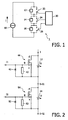
- Figure 1 diagrammatically shows a circuit arrangement according to the present invention.
- 10 denotes a current source for a current I in the direction of the arrow.
- Three electrical devices 12, 14, 16 are indicated as well as three switches 22, 24, 26, and a control unit 30.
- the current source 10 has been included in the circuit arrangement 1, but it is also possible to provide only a connection to an external current source.
- the current source is not particularly limited, but may be selected in accordance with the current and power requirements of the electrical devices used.
- the devices 12, 14, 16 are denoted only very generally, and their number may also be 2, as well as 4, 5, and upwards.
- every electrical device 12, 14, 16 has its own switch 22, 24, 26, respectively, connected in parallel with only one electrical device. Note that it is possible to provide additional electrical devices in series and/or in parallel to the three devices shown here.
- the switches 22, 24, 26 may also control each control more than one electrical device.
- the presently shown embodiment comprises for example three differently colored LEDs, for an RGB system.
- the control unit 30 is shown to control each switch 22, 24, 26, although it is possible to provide a control unit having several control sub-units that each control one or more of the plurality of switches 22, 24, 26.
- the control unit 30 will often be a computer or similar control circuitry.
- the invention relates to the effects that controlling the switches 22, 24 has on the control of downstream switches 24, 26, and correction of the latter control.
- FIG. 2 schematically shows a detail of a particular embodiment of the circuit arrangement of the present invention.
- 12 and 14 are a first and a second LED, respectively.
- a first and a second MOSFET switch have been indicated with 44 and 54, respectively.
- Each switch has a gate g, a drain d and a source s as indicated.
- a main current I, a first control current I 1 and a second control current I 2 are injected as indicated by the respective arrows.
- a current source (not indicated in the figure) injects a current I into the series connected LEDs.
- LED 12 is ON, which implies that there is a zero control current I 1 .
- I+I 1 1
- the second LED 14 receives the same current.
- the control current I 1 is added to the current I , and hence I+I 1 ⁇ I. This increased current is sent through the second LED 14.
- the control signal for the first LED in other words an upstream electrical device, influences every downstream LED (or electrical device).
- this may be corrected as follow.
- the control current I 1 is 0.02 I, and suppose furthermore that the intensity of the LED 12 and 14 depends linearly on current.
- the second LED 14 will now emit 2% more light. This may be corrected by switching off the second LED 14 during 2/102 x 100% ⁇ 2% of the time.
- a corresponding PWM control signal may be supplied to the second LED 14 in the form of a PWM second control current I 2 .
- This second control current I 2 may be supplied to the second switch 54 in a similar fashion as the first control current I 1 .
- the nett result is that the first LED 12 is switched off, while the second LED 14 emits with the same intensity as before.
- other devices downstream the second LED 14 may be controlled in a similar fashion in order to correct influences by the injected control currents I 1 , I 2 , et cetera.
- the "extra" control current is branched off from the main current I that re-enters the current source, by the provision of an electrical connection (not shown) back to the control unit. Via this connection, that closes a control circuit, the control current will flow.
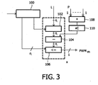
- FIG. 3 shows a flow diagram of a method according to the invention.
- a counter is indicated by 100, a width register 102, a subtractor by 104, a comparator by 106, an adder by 108 and a multiplicator by 110.
- counter 100 cyclically counts from 0 to 2 n -1, with n the number of bits used, i.e. the resolution.
- a desired pulse width is entered into the width register 102, via a clock controlled load-on-carry signal, i.e. the arrow from counter 100 to width register 102.
- This pulse width may also have a width of n bits, and its value may be based on the desired intensity of the LED.
- the comparator 106 would determine whether or not the counter 100 value was at least equal to the desired pulse width, in order to generate the HIGH value at the desired counter value. In other words, parts 104 and, of course 108 and 110, would not be present.
- this method is corrected.
- all pulse width modulation signals of upstream switches i.e. PWMO through PWM(m-1) are used.
- their values are added by adder 108, after which the added value is multiplied with a correction value c in multiplicator 110. The value thus obtained is subtracted form the width register value.
- the correction value c depends for example on a ratio of the average respective control current, such as I 1 in Fig. 2 , to the main current, such as the LED current I in Fig. 2 . This is based on the assumption that the LED intensity is linearly dependent of current. Of course, if other devices are used, a different dependency may prevail, and a different correction factor c, or even a different correction scheme may be utilized. As long as the dependency is known, however, this may be embodied in circuitry or a programmed computer, in order for the control current to be optimally corrected. In the case of e.g. a bipolar transistor, this factor c may include a correction due to the circumstance that only part of the control current passes through the resistive element, while another part passes through the transistor, as a gate current.
Landscapes
- Led Devices (AREA)
- Electronic Switches (AREA)
- Communication Control (AREA)
- Selective Calling Equipment (AREA)
- Control Of Indicators Other Than Cathode Ray Tubes (AREA)
- Power Conversion In General (AREA)
Abstract
Description
- The present invention relates to a circuit assembly, comprising a connection for an electrical current source for providing a constant electrical current to the circuit assembly, at least one first electrical device and at least one second electrical device, connected in series therewith, at least one semiconductor switch for controlling said first electrical device, and comprising at least a gate, a source and a drain, and connected in parallel with said first electrical device by means of the drain and the source, and a control unit arranged for providing a first control signal to the semiconductor switch and a second control signal to said second electrical device, wherein said second electrical device is present downstream of said first electrical device and said semiconductor switch, in the direction of a current flow when the circuit arrangement is in use.
- A series connection of transistor controlled electrical devices is well-known. For example,
US 6,153,980 discloses a LED array having an active shunt switch arrangement, wherein a plurality of LEDs connected in series each have an active shunt, such as a power MOSFET, connected there across. Digital logic is connected to each shunt switch, and serves to sequentially activate the active shunts. - Series connections of electrical devices are useful, in that the electrical current that passes through each device is the same. Since the performance of many types of electrical device depends on the current, this series connection is a useful feature to set the electrical working conditions for the devices.
- When using an active semiconductor switches in a series connected circuit arrangement of electrical devices, the following problem arises. The semiconductor switch is connected in parallel with the electrical device or devices with its source and its drain, while its gate is not so connected. The switch needs a certain voltage difference between its gate and source in order to be in a closed or open state, to hence determine whether to shunt the electrical device or not. However, the voltage at the source of a particular semiconductor switch depends on the state of the electrical devices upstream of that particular semiconductor switch, and especially of other semiconductor switches upstream of that particular semiconductor switch. Hence, by simply relying on providing a particular voltage at the gate, the above mentioned voltage difference is not well-defined, which is a disadvantage. For example, it may occur that both the semiconductor switch is partially conductive, which means there is an undesirable energy loss in the switch, and an unwanted situation.
- It is an object of the present invention to provide a circuit arrangement of the kind mentioned in the preamble, that is able to provide improved control over the performance of the semiconductor switch controlled electrical device(s).
- Said object is achieved according to the invention with a circuit arrangement of the type mentioned above, wherein at least one electrical component is provided between the gate and the source, across which electrical component a voltage difference develops when a current is sent through the component, wherein furthermore the first control signal comprises a control current signal to the gate and to the electrical component, wherein the first control current signal is substantially added to the electrical current, providing an increased current through said second electrical device, wherein the control unit is arranged to adapt the second control signal in dependence of the first control signal, to correct the influence of the added first control current on the second electrical device.
- Ordinarily, ways of providing a well-defined voltage difference that rely on providing a current across an electrical component interfere with the above mentioned advantage of an equal current for each electrical device in the series connection, because that current necessarily adds to the current through the parallel connection of electrical device and source-drain connection of the semiconductor switch. According to the invention, use is made of a local, floating voltage that creates a well-defined voltage difference across the semiconductor switch, while the effect of the current signal through the electrical component and into the series connection of electrical devices is corrected by having the control unit adapt the control signals for each semiconductor switch downstream of the switch under consideration. Note that this floating voltage is particularly useful in series connections of large numbers of devices, since otherwise it becomes increasingly difficult to supply a well-defined source voltage for the transistor, because the absolute voltages will change in dependence of control signals upstream.
- Note that simply providing an "absolute" voltage at the source or drain of the switch is not reliable, also because in cases where many electrical devices are connected in series, such as is often the case for e.g. multi-LED applications, the absolute value of said voltage will amount to the number of LEDs times the LED voltage, which may become several hundred volts. This cannot be tolerated for many semiconductor switches, e.g. due to specifications or safety regulations.
- According to the present invention, the effect of the extra current in the series connected electrical devices downstream is known, since this only depends on the properties of the electrical component and the current signal, which are known. Hence, it is possible for the control unit to predict the effect of the current signals upstream on the current downstream. The control signals for switches downstream are adapted in dependence of that knowledge, such as with a look-up table. Other methods will be described below.
- Although it suffices when a connection to a power source is provided, it may be even more advantageous to provide and include a power source. Preferably, the power source comprises a current source, providing a substantially constant current.
- In principle, each type of semiconductor switch is allowed in the present invention, such as a bipolar transistor. However, the invention is very advantageous for a circuit arrangement, wherein the semiconductor switch comprises an insulated gate transistor switch. In particular, the insulated gate transistor switch comprises a JFET or a MOSFET. In these cases, the effects and advantages may become apparent, in that the rise-time of these switches depends on the current between gate and source, since first a capacitance of the gate-source must be charged (or discharged) in order for the transistor to be able to switch from a non-conductive to a conductive state (or vice versa). When the current applied is very low, this may take a relatively long time, which is undesirable. The invention allows a good control over this period of time, by being able to adapt the circuit design towards a desired switch behavior, as will be explained below. It is remarked here that the current signal is of course divided between the electrical component across which a voltage is produced, and the gate of the semiconductor switch. However, in almost all cases, the gate (leak) current is so much lower than the current through the electrical component, that the gate current may be ignored for all practical purposes. However, for example in the case of a bipolar transistor, it will often be required to include the gate current. Depending on the transistor characteristics, a correction for the contribution of the gate current to the total control current may be made. This will be further elucidated in the description of preferred embodiments.
- Note that the at least one electrical component is meant to be a separate component, not an inherent non-physically separate "component", such as stray capacitance.
- In a special embodiment, the electrical component comprises a resistor. This is an extremely simple, small and cheap feature that still performs its duty, in that it develops a voltage across it when a (control) current flows through it. The voltage is very well controllable, as compared to other passive components, such as capacitors and inductances, although their use is not excluded.
- In particular, the resistor has a resistance of between 0.5 and 500 kΩ, preferably between 1 and 100 kΩ. With such values of the resistance, it can easily be ensured that the switch opens/closes sufficiently fast, in other words that the rise-time is sufficiently short for a reliable operation.
- In a special embodiment, the second electrical device comprises an additional insulated gate semiconductor switch, for controlling said second electrical device, and comprising at least a gate, a source and a drain, and connected in parallel with said second electrical device by means of the drain and the source. This arrangement has an advantage that the second electrical device may be controlled by the same control unit, and in the same way, as the first electrical device. Note that other ways of control, as well as other control units are possible as well. Note furthermore that a plurality of separate control units for controlling various electrical devices is deemed to be comprised in the expression "control unit" as used in this document.
- In a special embodiment, the first and/or second electrical device comprises a LED. LEDs are often used in large numbers, and furthermore are often used in a series connection, as they have a performance, viz. light output, that is rather dependent on current through the LED. Hence a critical control of the output of the LED is desirable, and can be obtained with the arrangement according to the invention.
- In a particular embodiment, the first and/or second control signal comprises a pulse width modulated (PWM) current signal having a duty cycle. As is known in the art, a pulse width modulation signal is a control signal that comprises pulses emitted in a regular fashion, with a predetermined frequency, and having a controllable width that determines the strength of the pulse. It may be normally HIGH or normally LOW. This type of control signal is used e.g. to be able to dim lamps and yet always have the same ON current, which is desirable in that the properties of the electrical device need to be known only in two situations, instead of a continuous range of (current) conditions. E.g., always having the same ON current ensures that the gate-source voltage difference is independent of other, upstream control currents. The switches will thus always switch equally fast, etc. Similar considerations hold for the circuit arrangement as a whole.
- In a special embodiment, the duty cycle of the second control signal is dependent of the first control signal. This is an elaboration of the invention, wherein for example a momentary value of the first control signal (for very fast adaptation of the second control signal) or an average value or duty cycle of the first control signal (for less fast adaptation of the second control signal) is used to adapt the duty cycle of the second control signal. In pulse width modulation, the duty cycle is used to express the percentage of the time that the signal value is not the standard value. For example, in the case of a normally LOW signal, if the frequency is 100 Hz, and hence the pulse time is 10 ms, and the signal is HIGH during 2 ms each pulse, the duty cycle is 0.2, or 20%. This may e.g. be used if it is desired to drive a LED at 20% of its nominal intensity value. Now suppose that one other LED upstream of this LED under consideration is switched to a different intensity value, then that corresponds to a different control signal of that other upstream LED. This in turn means that a different control current is sent into the series connection, and hence the total current as seen by the LED under consideration changes. Hence, a correction of the control signal to the LED under consideration has to be adapted, and the control current has to be made either higher or lower (at least on average), or similarly the duty cycle for the LED under consideration has to be adapted.
- The way in which other, upstream control signals are used to adapt a particular control signal is not limited. Often, a computer or similar circuitry can be provided, that is able to process the other, upstream control signals in order to determine an appropriate control signal. Thereto, knowledge of the total circuit arrangement may be used in the form of a look-up table, that states what control signal should be provided to a particular switch/device, knowing all upstream control signals. Alternatively, it is possible to use a current sensor device arranged to provide a current reading for the particular device, on the basis of which the control unit may determine the appropriate control signal. For example, in each of the above cases, a PWM signal for the particular switch/device may be adapted.
- In a particular embodiment, the circuit arrangement of the invention comprises a plurality of first and second electrical devices, that are connected in series, and a plurality of semiconductor switches that are each connected in parallel with one or more of the plurality of first and second electrical devices, wherein the control unit is arranged to provide each of the semiconductor switches with a respective control signal, and wherein the control unit is furthermore arranged to adapt the respective control signal of each particular semiconductor switch in dependence of all of the respective control signals for all of the semiconductor switches upstream said particular semiconductor switch. In this embodiment, the advantages of the invention are used in a more complex setting, in which for higher numbers of devices, in particular 10 or more, or even 50 or more, first and/or second devices, such as LEDs, are controlled by a number of transistors. It is repeated here that a particular advantage is that it is possible to define a suitable voltage difference between the gate and source of a particular semiconductor switch.
- Note that the number of first and/or second semiconductor switches need not correspond to the number of first and/or second electrical devices, since in each case one or more first and/or second electrical devices may be controlled by a single first or second semiconductor switch. It is also possible to consider this situation as one in which an electrical device comprises a plurality of subdevices.
- In a particular embodiment, the circuit arrangement comprises a first, second and third electrical device, connected in series, and each having connected in parallel thereto a respective semiconductor switch that is able to receive a respective control signal from a control unit, wherein the control signal for a particular semiconductor switch is dependent of the respective control signals for all semiconductor switches upstream of said particular semiconductor switch. Preferably, the first, second and third electrical devices each comprise LEDs of a different color. For example, the first devices are red LEDs, the second devices are green LEDs, and the third devices are blue LEDs. Even more preferably, the circuit arrangement further comprises a fourth LED, with a color that differs from the colors of the first, second and third LEDs. These embodiments are very advantageous for offering good color and intensity control of a LED arrangement. For example, the well known RGB system is used, having a red, a green and a blue LED. Alternatively, a fourth color is added, such as the RGBA system, in which an amber colored LED is added, for better color rendering. Note that it is also possible to add one or more additional sets of first through third, or even fourth, electrical devices, connected in series and/or parallel with the first set of first through third or fourth electrical devices. Advantageously, the additional sets also comprise semiconductor switches connected in accordance with the present invention.
- The present invention also. relates to a method of driving a circuit arrangement with at least one first electrical device and at least one second electrical device, connected in series therewith, by means of a semiconductor switch for controlling said first electrical device, and comprising at least a gate, a source and a drain, and connected in parallel with said first electrical device by means of the drain and the source, wherein said second electrical device is present downstream of said first electrical device and said semiconductor switch, in the direction of a constant current flow when the circuit arrangement is in use, the method comprising providing a first control signal between the gate and the source, that switches the semiconductor switch, in order to control the first electrical device, the first control signal comprising a first control current signal, wherein the first control current signal is substantially added to the electrical current, providing an increased current through said second electrical device; providing a second control signal to control the second electrical device, wherein the second control signal is determined in dependence of the first control signal, to correct the influence of the added first control current on the second electrical device. The advantages of this method over prior art methods correspond to the advantages of the circuit arrangement of the present invention. A discussion thereof has been given hereinabove. In particular, the method may be applied to the circuit arrangement of the present invention.
- In a particular embodiment, providing the first control signal comprises providing a resistive element between the gate and the source and providing a current signal through the resistive element, and wherein the second control signal is determined in dependence of the value of the current signal. Such a resistive element allows a simple, and cheap way of providing a well-defined voltage with an also well-defined current. By appropriately selecting a resistance value, the rise-time of the semiconductor switch may be sufficiently short. Suitable values are between about 500 Ω and 500 kΩ, in particular between about 1 and 100 kΩ.
- In a special method, a plurality of first and second electrical devices is provided, that are connected in series, as well as a plurality of semiconductor switches, that are each connected in parallel with one or more of the plurality of first and second electrical devices, and that each receive a respective control signal, wherein the respective control signal of each particular semiconductor switch is determined in dependence of all of the respective control signals for all of the semiconductor switches upstream said particular semiconductor switch. In this embodiment, the method of the invention is performed in a more complex situation, and provides all advantages of an individually adapted and corrected control signal for all devices that may be influenced by control signals upstream.
- These and other objects, features and advantages of the present invention may become more readily apparent from the following detailed description of non-limiting and exemplary embodiments, taken in conjunction with the drawing, in which:
-
Figure 1 diagrammatically shows a circuit arrangement according to the present invention. -
Figure 2 schematically shows a detail of a particular embodiment of the circuit arrangement of the present invention. -
Figure 3 shows a flow diagram of a method according to the invention. -
Figure 1 diagrammatically shows a circuit arrangement according to the present invention. - Herein, 10 denotes a current source for a current I in the direction of the arrow. Three
electrical devices switches control unit 30. As shown here, thecurrent source 10 has been included in thecircuit arrangement 1, but it is also possible to provide only a connection to an external current source. The current source is not particularly limited, but may be selected in accordance with the current and power requirements of the electrical devices used. - The
devices electrical device own switch switches - The
control unit 30 is shown to control eachswitch switches control unit 30 will often be a computer or similar control circuitry. - The invention relates to the effects that controlling the
switches downstream switches -
Figure 2 schematically shows a detail of a particular embodiment of the circuit arrangement of the present invention. Herein, 12 and 14 are a first and a second LED, respectively. A first and a second MOSFET switch have been indicated with 44 and 54, respectively. Each switch has a gate g, a drain d and a source s as indicated. - Two Zener-diodes and two resistors have been indicated with 40, 50 and 42, 52, respectively.
- Furthermore, a main current I, a first control current I1 and a second control current I2 are injected as indicated by the respective arrows.
- Suppose a current source (not indicated in the figure) injects a current I into the series connected LEDs. Suppose furthermore that
LED 12 is ON, which implies that there is a zero control current I1. Hence, I+I1 =1, and thesecond LED 14 receives the same current. - Suppose now that it is desired to switch off
LED 12. This may be achieved by injecting a control current I1 into thefirst switch 44. Injecting the control current I1 produces a voltage acrossresistor 42, which likewise produces a voltage between the gate g and the source s. Thereupon, after the rise-time of theswitch 44, theswitch 44 will start to conduct and shunt theLED 12. - The nett result is that the current I will not go through the LED, but go through the
switch 44, at least substantially. However, the control current I1 is added to the current I , and hence I+I1≈I. This increased current is sent through thesecond LED 14. This is a clear example that the control signal for the first LED, in other words an upstream electrical device, influences every downstream LED (or electrical device). However, according the invention, this may be corrected as follow. Suppose, for ease of calculation, that the control current I1 is 0.02 I, and suppose furthermore that the intensity of theLED second LED 14 will now emit 2% more light. This may be corrected by switching off thesecond LED 14 during 2/102 x 100% ≈ 2% of the time. A corresponding PWM control signal may be supplied to thesecond LED 14 in the form of a PWM second control current I2.This second control current I2 may be supplied to thesecond switch 54 in a similar fashion as the first control current I1. - In all, the nett result is that the
first LED 12 is switched off, while thesecond LED 14 emits with the same intensity as before. Of course, it is similarly possible to control eachLED second LED 14 may be controlled in a similar fashion in order to correct influences by the injected control currents I1, I2, et cetera. It is furthermore noted that the "extra" control current is branched off from the main current I that re-enters the current source, by the provision of an electrical connection (not shown) back to the control unit. Via this connection, that closes a control circuit, the control current will flow. -
Figure 3 shows a flow diagram of a method according to the invention. Herein, a counter is indicated by 100, awidth register 102, a subtractor by 104, a comparator by 106, an adder by 108 and a multiplicator by 110. - Briefly, counter 100 cyclically counts from 0 to 2n-1, with n the number of bits used, i.e. the resolution. For the switch m that is to be controlled by the pulse width modulated signal PWMm, a desired pulse width is entered into the
width register 102, via a clock controlled load-on-carry signal, i.e. the arrow fromcounter 100 towidth register 102. This pulse width may also have a width of n bits, and its value may be based on the desired intensity of the LED. In a non-corrected system, thecomparator 106 would determine whether or not thecounter 100 value was at least equal to the desired pulse width, in order to generate the HIGH value at the desired counter value. In other words,parts 104 and, ofcourse - According to the invention, this method is corrected. In this case, all pulse width modulation signals of upstream switches, i.e. PWMO through PWM(m-1), are used. In order to incorporate their effect on the PWMm, their values are added by
adder 108, after which the added value is multiplied with a correction value c inmultiplicator 110. The value thus obtained is subtracted form the width register value. - The correction value c depends for example on a ratio of the average respective control current, such as I1 in
Fig. 2 , to the main current, such as the LED current I inFig. 2 . This is based on the assumption that the LED intensity is linearly dependent of current. Of course, if other devices are used, a different dependency may prevail, and a different correction factor c, or even a different correction scheme may be utilized. As long as the dependency is known, however, this may be embodied in circuitry or a programmed computer, in order for the control current to be optimally corrected. In the case of e.g. a bipolar transistor, this factor c may include a correction due to the circumstance that only part of the control current passes through the resistive element, while another part passes through the transistor, as a gate current.
Claims (15)
- A circuit assembly (1), comprising- a connection for a current source (10) for providing a constant electrical current (I) to the circuit assembly,- at least one first electrical device (12, 14) and at least one second electrical device (14, 16), connected in series therewith, as circuit assembly- at least one semiconductor switch (22, 24) for controlling said first electrical device (12, 14), and comprising at least a gate (g), a source (s) and a drain (d), and connected in parallel with said first electrical device (12, 14) by means of the drain (d) and the source (s),- a control unit (30) arranged for providing a first control signal to the semiconductor switch (22, 24) and a second control signal to said second electrical device (14, 16),wherein said second electrical device (14, 16) is present downstream of said first electrical device (12, 14) and said semiconductor switch (22, 24), in the direction of a current flow when the circuit arrangement is in use,
wherein at least one electrical component (40, 42, 50, 52) is provided between the gate (g) and the source (d), across which electrical component a voltage difference develops when a current (I, I1, I2) is sent through the component,
wherein furthermore the first control signal comprises a first control current signal (I1) to the gate (g) and to the electrical component (40, 42, 50, 52),
wherein the first control current signal (I1) is substantially added to the electrical current (I), providing an increased current (I+I1) through said second electrical device (14, 16),
wherein the control unit (30) adapts the second control signal in dependence of the first control signal, to correct the influence of the added first control current (I1) on the second electrical device (14, 16). - The circuit arrangement of claim 1, wherein the semiconductor switch (22, 24, 26) comprises an insulated gate transistor switch.
- The circuit arrangement of claim 2, wherein the insulated gate transistor (22, 24, 26; 44, 54) switch comprises a JFET or a MOSFET.
- The circuit arrangement of any preceding claim, wherein the electrical component comprises a resistor (42, 44).
- The circuit arrangement of claim 4, wherein the resistance has a value of between 0.5 and 500 kΩ, preferably between 1 and 100 kΩ.
- The circuit arrangement of any preceding claim, wherein the second electrical device (14, 16) comprises an additional insulated gate semiconductor switch (54), for controlling said second electrical device (14), and comprising at least a gate (g), a source (s) and a drain (d), and connected in parallel with said second electrical (14) device by means of the drain (d) and the source (s).
- The circuit arrangement of any preceding claim, wherein the first and/or second electrical device comprises a LED (12, 14).
- The circuit arrangement of any preceding claim, wherein the first and/or second control signal comprises a pulse width modulated current signal having a duty cycle.
- The circuit arrangement of claim 8, wherein the duty cycle of the second control signal is dependent of the first control signal.
- The circuit arrangement of any preceding claim, comprising a plurality of first and second electrical devices (12, 14, 16), that are connected in series, and a plurality of semiconductor switches (22, 24, 26) that are each connected in parallel with one or more of the plurality of first and second electrical devices (12, 14, 16),
wherein the control unit (30) is arranged to provide each of the semiconductor switches with a respective control signal, each control signal comprising a control current signal that is added to the electrical current (I), and
wherein the control unit (30) is furthermore arranged to adapt the respective control signal of each particular semiconductor switch (24, 26) in dependence of all of the respective control signals for all of the semiconductor switches (22, 24) upstream said particular semiconductor switch (24, 26), to correct the influences of the added control current signals. - The circuit arrangement of any preceding claim, wherein the circuit arrangement comprises a first, second and third electrical device (12, 14, 16), connected in series, and each having connected in parallel thereto a first, second and third semiconductor switch (22, 24, 26) that is able to receive a respective first, second and third control signal from a control unit (30),
wherein the first control signal comprises a first control current signal (I1), wherein the first control current signal (I1) is substantially added to the electrical current (I), providing an increased current (I+I1),
wherein the second control signal comprises a second control current signal (I2), wherein the second control current signal (I2) is substantially added to the electrical current (I), providing an increased current (I+I2),
wherein the control unit (30) is arranged to adapt the second control signal in dependence of the first control signal, to correct the influence of the added first control current (I1), and wherein the control unit (30) is arranged to adapt the third control signal in dependence of the second control signal, to correct the influence of the added second control current (I2). - Method of driving a circuit arrangement (1) with at least one first electrical device (12) and at least one second electrical device (14, 16) connected in series therewith, by means of a semiconductor switch (22; 44) for controlling said first electrical device (12), the semiconductor switch comprising at least a gate (g), a source (s) and a drain (d), and connected in parallel with said first electrical device (12) by means of the drain and the source, wherein said second electrical device (14, 16) is present downstream of said first electrical device (12) and said semiconductor switch (22; 44), in the direction of a constant current flow of an electrical current (I) when the circuit arrangement is in use,
the method comprising- providing a first control signal between the gate (g) and the source (s), that switches the semiconductor switch (22; 44), in order to control the first electrical device (12), the first control signal comprising a first control current signal (I1), wherein the first control current signal (I1) is substantially added to the electrical current (I), providing an increased current (I+I1) through said second electrical device (14, 16);- providing a second control signal to control the second electrical device (14, 16),wherein the second control signal is determined in dependence of the first control signal, to correct the influence of the added first control current (I1) on the second electrical device (14, 16). - The method of claim 12, wherein the circuit arrangement is the circuit arrangement (1) of any of claims 1-10.
- The method of claim 12 or 13, wherein providing the first control signal (I1) comprises providing a resistive element (42, 52) between the gate (g) and the source (s) and providing a current signal through the resistive element (42, 52),
and wherein the second control signal (I2) is determined in dependence of the value of the current signal (I1). - The method of any of claims 12-14, wherein a plurality of first and second electrical devices is provided, that are connected in series, as well as a plurality of semiconductor switches, that are each connected in parallel with one or more of the plurality of first and second electrical devices, and that each receive a respective control signal, each control signal comprising a control current signal that is added to the electrical current (I), wherein the respective control signal of each particular semiconductor switch (14, 16) is determined in dependence of all of the respective control signals for all of the semiconductor switches (12) upstream said particular semiconductor switch (14, 16), to correct the influences of the added control current signals.
Priority Applications (1)
| Application Number | Priority Date | Filing Date | Title |
|---|---|---|---|
| EP06821274A EP1949764B1 (en) | 2005-11-08 | 2006-11-01 | Circuit arrangement and method of driving a circuit arrangement |
Applications Claiming Priority (3)
| Application Number | Priority Date | Filing Date | Title |
|---|---|---|---|
| EP05110481 | 2005-11-08 | ||
| PCT/IB2006/054038 WO2007054856A2 (en) | 2005-11-08 | 2006-11-01 | Circuit arrangement and method of driving a circuit arrangement |
| EP06821274A EP1949764B1 (en) | 2005-11-08 | 2006-11-01 | Circuit arrangement and method of driving a circuit arrangement |
Publications (2)
| Publication Number | Publication Date |
|---|---|
| EP1949764A2 EP1949764A2 (en) | 2008-07-30 |
| EP1949764B1 true EP1949764B1 (en) | 2011-04-06 |
Family
ID=38023646
Family Applications (1)
| Application Number | Title | Priority Date | Filing Date |
|---|---|---|---|
| EP06821274A Not-in-force EP1949764B1 (en) | 2005-11-08 | 2006-11-01 | Circuit arrangement and method of driving a circuit arrangement |
Country Status (10)
| Country | Link |
|---|---|
| US (1) | US7834678B2 (en) |
| EP (1) | EP1949764B1 (en) |
| JP (1) | JP4975038B2 (en) |
| KR (1) | KR20080075163A (en) |
| CN (1) | CN101305642B (en) |
| AT (1) | ATE505056T1 (en) |
| DE (1) | DE602006021218D1 (en) |
| ES (1) | ES2364082T3 (en) |
| TW (1) | TW200733794A (en) |
| WO (1) | WO2007054856A2 (en) |
Families Citing this family (16)
| Publication number | Priority date | Publication date | Assignee | Title |
|---|---|---|---|---|
| US8791645B2 (en) | 2006-02-10 | 2014-07-29 | Honeywell International Inc. | Systems and methods for controlling light sources |
| US8188679B2 (en) | 2007-07-23 | 2012-05-29 | Nxp B.V. | Self-powered LED bypass-switch configuration |
| ES2457444T3 (en) * | 2008-05-20 | 2014-04-25 | Eldolab Holding B.V. | Controller to control a set of LEDs, a lighting application and a procedure to control a set of LEDs |
| WO2010079635A1 (en) * | 2009-01-09 | 2010-07-15 | シャープ株式会社 | Light-emitting diode driving circuit and sheet-like illuminating device having same |
| CN102006699B (en) * | 2009-09-02 | 2013-04-17 | 海洋王照明科技股份有限公司 | Police photo-taking light circuit |
| TWI422278B (en) * | 2010-05-25 | 2014-01-01 | Optromax Electronics Co Ltd | Illuminating apparatus and light source control circuit thereof |
| US9871404B2 (en) * | 2011-12-12 | 2018-01-16 | Cree, Inc. | Emergency lighting devices with LED strings |
| US10117295B2 (en) | 2013-01-24 | 2018-10-30 | Cree, Inc. | LED lighting apparatus for use with AC-output lighting ballasts |
| DE102012201415A1 (en) * | 2012-02-01 | 2013-08-01 | Osram Gmbh | Circuit arrangement, light unit for a vehicle and method for driving semiconductor light elements |
| US8415887B1 (en) * | 2012-10-20 | 2013-04-09 | Jlj, Inc. | Transistor bypass shunts for LED light strings |
| DE102012223816B3 (en) * | 2012-12-19 | 2014-06-12 | Continental Automotive Gmbh | Device for driving a field effect transistor |
| US10026574B2 (en) | 2013-03-18 | 2018-07-17 | Infineon Technologies Ag | Multi-load drive circuit |
| US9265102B2 (en) * | 2014-03-07 | 2016-02-16 | Iml International | Light-emitting diode lighting device with adjustable color rendering indexes |
| TWI513367B (en) * | 2014-07-15 | 2015-12-11 | Groups Tech Co Ltd | Electronic control gears for led light engine and application thereof |
| CN103926441B (en) * | 2014-04-25 | 2017-03-22 | 湖南银河电气有限公司 | Novel voltage divider |
| CN110149110B (en) * | 2018-02-11 | 2020-08-25 | 陶顺祝 | Drive circuit of electronic switch series structure |
Family Cites Families (18)
| Publication number | Priority date | Publication date | Assignee | Title |
|---|---|---|---|---|
| US4743897A (en) * | 1985-10-09 | 1988-05-10 | Mitel Corp. | LED driver circuit |
| JPH01104754U (en) * | 1988-01-06 | 1989-07-14 | ||
| JP2991893B2 (en) | 1993-05-31 | 1999-12-20 | 富士通株式会社 | Driving circuit for light emitting element and optical amplification repeater using the same |
| EP0845815A3 (en) * | 1996-11-28 | 1999-03-03 | Matsushita Electric Industrial Co., Ltd. | Semiconductor device, method of designing the same and semiconductor integrated circuit device |
| US6153980A (en) * | 1999-11-04 | 2000-11-28 | Philips Electronics North America Corporation | LED array having an active shunt arrangement |
| DE10018760A1 (en) | 2000-04-15 | 2001-10-18 | Volkswagen Ag | Circuit for monitoring light emitting diode function has associated light sensitive component subjected to light from light emitting diodes and influencing current through light emitting diode |
| US7202613B2 (en) * | 2001-05-30 | 2007-04-10 | Color Kinetics Incorporated | Controlled lighting methods and apparatus |
| DE10103611B4 (en) | 2001-01-26 | 2013-12-19 | Insta Elektro Gmbh | Circuit arrangement for operating a plurality of bulbs |
| JP2002246886A (en) * | 2001-02-13 | 2002-08-30 | Auto Network Gijutsu Kenkyusho:Kk | Semiconductor circuit component |
| US20020175826A1 (en) * | 2001-04-05 | 2002-11-28 | Hutchison Michael C. | Traffic signal having electronically reconfigurable LED array |
| JP3666423B2 (en) * | 2001-07-06 | 2005-06-29 | 日本電気株式会社 | Driving circuit |
| US20040090403A1 (en) * | 2002-11-08 | 2004-05-13 | Dynascan Technology Corp. | Light-emitting diode display apparatus with low electromagnetic display |
| US7015825B2 (en) * | 2003-04-14 | 2006-03-21 | Carpenter Decorating Co., Inc. | Decorative lighting system and decorative illumination device |
| US20050062481A1 (en) * | 2003-09-19 | 2005-03-24 | Thomas Vaughn | Wayside LED signal for railroad and transit applications |
| DE10358447B3 (en) * | 2003-12-13 | 2005-05-25 | Insta Elektro Gmbh | Illumination device has series LEDs, each with parallel-connected electronic unit with low impedance switch element, diode, threshold switch, capacitor whose voltage supplies threshold switch and is fed to threshold switch as its input |
| JP4720100B2 (en) * | 2004-04-20 | 2011-07-13 | ソニー株式会社 | LED driving device, backlight light source device, and color liquid crystal display device |
| JP4241487B2 (en) * | 2004-04-20 | 2009-03-18 | ソニー株式会社 | LED driving device, backlight light source device, and color liquid crystal display device |
| US7633463B2 (en) * | 2004-04-30 | 2009-12-15 | Analog Devices, Inc. | Method and IC driver for series connected R, G, B LEDs |
-
2006
- 2006-11-01 EP EP06821274A patent/EP1949764B1/en not_active Not-in-force
- 2006-11-01 WO PCT/IB2006/054038 patent/WO2007054856A2/en active Application Filing
- 2006-11-01 KR KR1020087013723A patent/KR20080075163A/en not_active Application Discontinuation
- 2006-11-01 AT AT06821274T patent/ATE505056T1/en not_active IP Right Cessation
- 2006-11-01 US US12/092,750 patent/US7834678B2/en not_active Expired - Fee Related
- 2006-11-01 CN CN200680041794XA patent/CN101305642B/en not_active Expired - Fee Related
- 2006-11-01 ES ES06821274T patent/ES2364082T3/en active Active
- 2006-11-01 DE DE602006021218T patent/DE602006021218D1/en active Active
- 2006-11-01 JP JP2008538478A patent/JP4975038B2/en not_active Expired - Fee Related
- 2006-11-03 TW TW095140909A patent/TW200733794A/en unknown
Also Published As
| Publication number | Publication date |
|---|---|
| WO2007054856A2 (en) | 2007-05-18 |
| CN101305642A (en) | 2008-11-12 |
| US20080265981A1 (en) | 2008-10-30 |
| JP4975038B2 (en) | 2012-07-11 |
| JP2009515405A (en) | 2009-04-09 |
| DE602006021218D1 (en) | 2011-05-19 |
| CN101305642B (en) | 2010-11-17 |
| EP1949764A2 (en) | 2008-07-30 |
| WO2007054856A3 (en) | 2007-10-11 |
| US7834678B2 (en) | 2010-11-16 |
| ATE505056T1 (en) | 2011-04-15 |
| KR20080075163A (en) | 2008-08-14 |
| ES2364082T3 (en) | 2011-08-24 |
| TW200733794A (en) | 2007-09-01 |
Similar Documents
| Publication | Publication Date | Title |
|---|---|---|
| EP1949764B1 (en) | Circuit arrangement and method of driving a circuit arrangement | |
| KR101315078B1 (en) | Led lighting device | |
| US7741788B2 (en) | Light emitting apparatus with current limiting | |
| US7088059B2 (en) | Modulated control circuit and method for current-limited dimming and color mixing of display and illumination systems | |
| US8111014B2 (en) | Drive circuit for driving a load with constant current | |
| JP4776596B2 (en) | Lighting control device for vehicle lamp | |
| US7746300B2 (en) | Circuit and methodology for supplying pulsed current to a load, such as a light emitting diode | |
| US20100079074A1 (en) | Light Emitting Driver Circuit with Bypass and Method | |
| CN104798306B (en) | Device for controlling a field effect transistor | |
| EP2437134B1 (en) | Low electromagnetic emission driver | |
| KR20190005927A (en) | Automotive lighting | |
| KR101400475B1 (en) | LED driving circuit comprising delay time circuit to a current source | |
| US10015857B2 (en) | Method and apparatus for reducing flickering of emitted light | |
| JP6011011B2 (en) | Lighting device, lighting device, and dimming method | |
| US20140247033A1 (en) | Low EMI Driver Circuit | |
| US11343891B2 (en) | LED system for vehicle lighting having high efficiency and high reliability | |
| US20180177013A1 (en) | Illuminating device for vehicles | |
| US11291094B2 (en) | LED driving circuit | |
| US8084961B2 (en) | Backlight module control system and control method thereof | |
| EP3448125B1 (en) | Lighting system, and related lighting module | |
| WO2010037015A1 (en) | Light emitting driver circuit with compensation and method | |
| KR101473797B1 (en) | LED drive circuit connected directly to the AC power for the LED is turned on in the same way. | |
| WO2017099593A1 (en) | Control circuit for an led fixture |
Legal Events
| Date | Code | Title | Description |
|---|---|---|---|
| PUAI | Public reference made under article 153(3) epc to a published international application that has entered the european phase |
Free format text: ORIGINAL CODE: 0009012 |
|
| 17P | Request for examination filed |
Effective date: 20080609 |
|
| AK | Designated contracting states |
Kind code of ref document: A2 Designated state(s): AT BE BG CH CY CZ DE DK EE ES FI FR GB GR HU IE IS IT LI LT LU LV MC NL PL PT RO SE SI SK TR |
|
| 17Q | First examination report despatched |
Effective date: 20090205 |
|
| GRAP | Despatch of communication of intention to grant a patent |
Free format text: ORIGINAL CODE: EPIDOSNIGR1 |
|
| GRAS | Grant fee paid |
Free format text: ORIGINAL CODE: EPIDOSNIGR3 |
|
| GRAA | (expected) grant |
Free format text: ORIGINAL CODE: 0009210 |
|
| AK | Designated contracting states |
Kind code of ref document: B1 Designated state(s): AT BE BG CH CY CZ DE DK EE ES FI FR GB GR HU IE IS IT LI LT LU LV MC NL PL PT RO SE SI SK TR |
|
| REG | Reference to a national code |
Ref country code: GB Ref legal event code: FG4D |
|
| REG | Reference to a national code |
Ref country code: CH Ref legal event code: EP |
|
| REG | Reference to a national code |
Ref country code: IE Ref legal event code: FG4D |
|
| REF | Corresponds to: |
Ref document number: 602006021218 Country of ref document: DE Date of ref document: 20110519 Kind code of ref document: P |
|
| REG | Reference to a national code |
Ref country code: DE Ref legal event code: R096 Ref document number: 602006021218 Country of ref document: DE Effective date: 20110519 |
|
| REG | Reference to a national code |
Ref country code: NL Ref legal event code: VDEP Effective date: 20110406 |
|
| REG | Reference to a national code |
Ref country code: ES Ref legal event code: FG2A Ref document number: 2364082 Country of ref document: ES Kind code of ref document: T3 Effective date: 20110824 |
|
| PG25 | Lapsed in a contracting state [announced via postgrant information from national office to epo] |
Ref country code: SI Free format text: LAPSE BECAUSE OF FAILURE TO SUBMIT A TRANSLATION OF THE DESCRIPTION OR TO PAY THE FEE WITHIN THE PRESCRIBED TIME-LIMIT Effective date: 20110406 |
|
| LTIE | Lt: invalidation of european patent or patent extension |
Effective date: 20110406 |
|
| PG25 | Lapsed in a contracting state [announced via postgrant information from national office to epo] |
Ref country code: LT Free format text: LAPSE BECAUSE OF FAILURE TO SUBMIT A TRANSLATION OF THE DESCRIPTION OR TO PAY THE FEE WITHIN THE PRESCRIBED TIME-LIMIT Effective date: 20110406 Ref country code: PT Free format text: LAPSE BECAUSE OF FAILURE TO SUBMIT A TRANSLATION OF THE DESCRIPTION OR TO PAY THE FEE WITHIN THE PRESCRIBED TIME-LIMIT Effective date: 20110808 Ref country code: SE Free format text: LAPSE BECAUSE OF FAILURE TO SUBMIT A TRANSLATION OF THE DESCRIPTION OR TO PAY THE FEE WITHIN THE PRESCRIBED TIME-LIMIT Effective date: 20110406 |
|
| PG25 | Lapsed in a contracting state [announced via postgrant information from national office to epo] |
Ref country code: CY Free format text: LAPSE BECAUSE OF FAILURE TO SUBMIT A TRANSLATION OF THE DESCRIPTION OR TO PAY THE FEE WITHIN THE PRESCRIBED TIME-LIMIT Effective date: 20110406 Ref country code: AT Free format text: LAPSE BECAUSE OF FAILURE TO SUBMIT A TRANSLATION OF THE DESCRIPTION OR TO PAY THE FEE WITHIN THE PRESCRIBED TIME-LIMIT Effective date: 20110406 Ref country code: LV Free format text: LAPSE BECAUSE OF FAILURE TO SUBMIT A TRANSLATION OF THE DESCRIPTION OR TO PAY THE FEE WITHIN THE PRESCRIBED TIME-LIMIT Effective date: 20110406 Ref country code: IS Free format text: LAPSE BECAUSE OF FAILURE TO SUBMIT A TRANSLATION OF THE DESCRIPTION OR TO PAY THE FEE WITHIN THE PRESCRIBED TIME-LIMIT Effective date: 20110806 Ref country code: FI Free format text: LAPSE BECAUSE OF FAILURE TO SUBMIT A TRANSLATION OF THE DESCRIPTION OR TO PAY THE FEE WITHIN THE PRESCRIBED TIME-LIMIT Effective date: 20110406 Ref country code: BE Free format text: LAPSE BECAUSE OF FAILURE TO SUBMIT A TRANSLATION OF THE DESCRIPTION OR TO PAY THE FEE WITHIN THE PRESCRIBED TIME-LIMIT Effective date: 20110406 Ref country code: GR Free format text: LAPSE BECAUSE OF FAILURE TO SUBMIT A TRANSLATION OF THE DESCRIPTION OR TO PAY THE FEE WITHIN THE PRESCRIBED TIME-LIMIT Effective date: 20110707 |
|
| PG25 | Lapsed in a contracting state [announced via postgrant information from national office to epo] |
Ref country code: NL Free format text: LAPSE BECAUSE OF FAILURE TO SUBMIT A TRANSLATION OF THE DESCRIPTION OR TO PAY THE FEE WITHIN THE PRESCRIBED TIME-LIMIT Effective date: 20110406 |
|
| PG25 | Lapsed in a contracting state [announced via postgrant information from national office to epo] |
Ref country code: CZ Free format text: LAPSE BECAUSE OF FAILURE TO SUBMIT A TRANSLATION OF THE DESCRIPTION OR TO PAY THE FEE WITHIN THE PRESCRIBED TIME-LIMIT Effective date: 20110406 Ref country code: EE Free format text: LAPSE BECAUSE OF FAILURE TO SUBMIT A TRANSLATION OF THE DESCRIPTION OR TO PAY THE FEE WITHIN THE PRESCRIBED TIME-LIMIT Effective date: 20110406 |
|
| PLBE | No opposition filed within time limit |
Free format text: ORIGINAL CODE: 0009261 |
|
| STAA | Information on the status of an ep patent application or granted ep patent |
Free format text: STATUS: NO OPPOSITION FILED WITHIN TIME LIMIT |
|
| PG25 | Lapsed in a contracting state [announced via postgrant information from national office to epo] |
Ref country code: PL Free format text: LAPSE BECAUSE OF FAILURE TO SUBMIT A TRANSLATION OF THE DESCRIPTION OR TO PAY THE FEE WITHIN THE PRESCRIBED TIME-LIMIT Effective date: 20110406 Ref country code: RO Free format text: LAPSE BECAUSE OF FAILURE TO SUBMIT A TRANSLATION OF THE DESCRIPTION OR TO PAY THE FEE WITHIN THE PRESCRIBED TIME-LIMIT Effective date: 20110406 Ref country code: SK Free format text: LAPSE BECAUSE OF FAILURE TO SUBMIT A TRANSLATION OF THE DESCRIPTION OR TO PAY THE FEE WITHIN THE PRESCRIBED TIME-LIMIT Effective date: 20110406 Ref country code: DK Free format text: LAPSE BECAUSE OF FAILURE TO SUBMIT A TRANSLATION OF THE DESCRIPTION OR TO PAY THE FEE WITHIN THE PRESCRIBED TIME-LIMIT Effective date: 20110406 |
|
| 26N | No opposition filed |
Effective date: 20120110 |
|
| REG | Reference to a national code |
Ref country code: DE Ref legal event code: R097 Ref document number: 602006021218 Country of ref document: DE Effective date: 20120110 |
|
| PG25 | Lapsed in a contracting state [announced via postgrant information from national office to epo] |
Ref country code: MC Free format text: LAPSE BECAUSE OF NON-PAYMENT OF DUE FEES Effective date: 20111130 |
|
| REG | Reference to a national code |
Ref country code: CH Ref legal event code: PL |
|
| PG25 | Lapsed in a contracting state [announced via postgrant information from national office to epo] |
Ref country code: CH Free format text: LAPSE BECAUSE OF NON-PAYMENT OF DUE FEES Effective date: 20111130 Ref country code: LI Free format text: LAPSE BECAUSE OF NON-PAYMENT OF DUE FEES Effective date: 20111130 |
|
| REG | Reference to a national code |
Ref country code: IE Ref legal event code: MM4A |
|
| PG25 | Lapsed in a contracting state [announced via postgrant information from national office to epo] |
Ref country code: IE Free format text: LAPSE BECAUSE OF NON-PAYMENT OF DUE FEES Effective date: 20111101 |
|
| PGFP | Annual fee paid to national office [announced via postgrant information from national office to epo] |
Ref country code: IT Payment date: 20121122 Year of fee payment: 7 Ref country code: ES Payment date: 20121221 Year of fee payment: 7 |
|
| PG25 | Lapsed in a contracting state [announced via postgrant information from national office to epo] |
Ref country code: LU Free format text: LAPSE BECAUSE OF NON-PAYMENT OF DUE FEES Effective date: 20111101 |
|
| PG25 | Lapsed in a contracting state [announced via postgrant information from national office to epo] |
Ref country code: BG Free format text: LAPSE BECAUSE OF FAILURE TO SUBMIT A TRANSLATION OF THE DESCRIPTION OR TO PAY THE FEE WITHIN THE PRESCRIBED TIME-LIMIT Effective date: 20110706 |
|
| PG25 | Lapsed in a contracting state [announced via postgrant information from national office to epo] |
Ref country code: TR Free format text: LAPSE BECAUSE OF FAILURE TO SUBMIT A TRANSLATION OF THE DESCRIPTION OR TO PAY THE FEE WITHIN THE PRESCRIBED TIME-LIMIT Effective date: 20110406 |
|
| PG25 | Lapsed in a contracting state [announced via postgrant information from national office to epo] |
Ref country code: HU Free format text: LAPSE BECAUSE OF FAILURE TO SUBMIT A TRANSLATION OF THE DESCRIPTION OR TO PAY THE FEE WITHIN THE PRESCRIBED TIME-LIMIT Effective date: 20110406 |
|
| REG | Reference to a national code |
Ref country code: DE Ref legal event code: R082 Ref document number: 602006021218 Country of ref document: DE Representative=s name: MEISSNER, BOLTE & PARTNER GBR, DE |
|
| REG | Reference to a national code |
Ref country code: DE Ref legal event code: R082 Ref document number: 602006021218 Country of ref document: DE Representative=s name: MEISSNER BOLTE PATENTANWAELTE RECHTSANWAELTE P, DE Effective date: 20140328 Ref country code: DE Ref legal event code: R081 Ref document number: 602006021218 Country of ref document: DE Owner name: PHILIPS LIGHTING HOLDING B.V., NL Free format text: FORMER OWNER: KONINKLIJKE PHILIPS ELECTRONICS N.V., EINDHOVEN, NL Effective date: 20140328 Ref country code: DE Ref legal event code: R082 Ref document number: 602006021218 Country of ref document: DE Representative=s name: MEISSNER, BOLTE & PARTNER GBR, DE Effective date: 20140328 Ref country code: DE Ref legal event code: R081 Ref document number: 602006021218 Country of ref document: DE Owner name: KONINKLIJKE PHILIPS N.V., NL Free format text: FORMER OWNER: KONINKLIJKE PHILIPS ELECTRONICS N.V., EINDHOVEN, NL Effective date: 20140328 |
|
| PG25 | Lapsed in a contracting state [announced via postgrant information from national office to epo] |
Ref country code: IT Free format text: LAPSE BECAUSE OF NON-PAYMENT OF DUE FEES Effective date: 20131101 |
|
| REG | Reference to a national code |
Ref country code: FR Ref legal event code: CA Effective date: 20141126 Ref country code: FR Ref legal event code: CD Owner name: KONINKLIJKE PHILIPS ELECTRONICS N.V., NL Effective date: 20141126 |
|
| REG | Reference to a national code |
Ref country code: ES Ref legal event code: FD2A Effective date: 20150708 |
|
| PG25 | Lapsed in a contracting state [announced via postgrant information from national office to epo] |
Ref country code: ES Free format text: LAPSE BECAUSE OF NON-PAYMENT OF DUE FEES Effective date: 20131102 |
|
| REG | Reference to a national code |
Ref country code: FR Ref legal event code: PLFP Year of fee payment: 10 |
|
| REG | Reference to a national code |
Ref country code: GB Ref legal event code: 732E Free format text: REGISTERED BETWEEN 20161006 AND 20161012 |
|
| REG | Reference to a national code |
Ref country code: FR Ref legal event code: PLFP Year of fee payment: 11 |
|
| PGFP | Annual fee paid to national office [announced via postgrant information from national office to epo] |
Ref country code: GB Payment date: 20161130 Year of fee payment: 11 Ref country code: FR Payment date: 20161129 Year of fee payment: 11 |
|
| REG | Reference to a national code |
Ref country code: DE Ref legal event code: R082 Ref document number: 602006021218 Country of ref document: DE Representative=s name: MEISSNER BOLTE PATENTANWAELTE RECHTSANWAELTE P, DE Ref country code: DE Ref legal event code: R081 Ref document number: 602006021218 Country of ref document: DE Owner name: PHILIPS LIGHTING HOLDING B.V., NL Free format text: FORMER OWNER: KONINKLIJKE PHILIPS N.V., EINDHOVEN, NL |
|
| PGFP | Annual fee paid to national office [announced via postgrant information from national office to epo] |
Ref country code: DE Payment date: 20170131 Year of fee payment: 11 |
|
| REG | Reference to a national code |
Ref country code: DE Ref legal event code: R119 Ref document number: 602006021218 Country of ref document: DE |
|
| GBPC | Gb: european patent ceased through non-payment of renewal fee |
Effective date: 20171101 |
|
| REG | Reference to a national code |
Ref country code: FR Ref legal event code: ST Effective date: 20180731 |
|
| PG25 | Lapsed in a contracting state [announced via postgrant information from national office to epo] |
Ref country code: DE Free format text: LAPSE BECAUSE OF NON-PAYMENT OF DUE FEES Effective date: 20180602 Ref country code: FR Free format text: LAPSE BECAUSE OF NON-PAYMENT OF DUE FEES Effective date: 20171130 |
|
| PG25 | Lapsed in a contracting state [announced via postgrant information from national office to epo] |
Ref country code: GB Free format text: LAPSE BECAUSE OF NON-PAYMENT OF DUE FEES Effective date: 20171101 |