EP1947764A1 - Acoustic surface wave element and acoustic surface wave device - Google Patents
Acoustic surface wave element and acoustic surface wave device Download PDFInfo
- Publication number
- EP1947764A1 EP1947764A1 EP06810328A EP06810328A EP1947764A1 EP 1947764 A1 EP1947764 A1 EP 1947764A1 EP 06810328 A EP06810328 A EP 06810328A EP 06810328 A EP06810328 A EP 06810328A EP 1947764 A1 EP1947764 A1 EP 1947764A1
- Authority
- EP
- European Patent Office
- Prior art keywords
- conductor layer
- electrode
- piezoelectric substrate
- acoustic wave
- layer
- Prior art date
- Legal status (The legal status is an assumption and is not a legal conclusion. Google has not performed a legal analysis and makes no representation as to the accuracy of the status listed.)
- Granted
Links
Images




Classifications
-
- H—ELECTRICITY
- H03—ELECTRONIC CIRCUITRY
- H03H—IMPEDANCE NETWORKS, e.g. RESONANT CIRCUITS; RESONATORS
- H03H9/00—Networks comprising electromechanical or electro-acoustic elements; Electromechanical resonators
- H03H9/02—Details
- H03H9/02535—Details of surface acoustic wave devices
- H03H9/02818—Means for compensation or elimination of undesirable effects
- H03H9/02834—Means for compensation or elimination of undesirable effects of temperature influence
-
- H—ELECTRICITY
- H03—ELECTRONIC CIRCUITRY
- H03H—IMPEDANCE NETWORKS, e.g. RESONANT CIRCUITS; RESONATORS
- H03H9/00—Networks comprising electromechanical or electro-acoustic elements; Electromechanical resonators
- H03H9/02—Details
- H03H9/125—Driving means, e.g. electrodes, coils
- H03H9/145—Driving means, e.g. electrodes, coils for networks using surface acoustic waves
- H03H9/14538—Formation
- H03H9/14541—Multilayer finger or busbar electrode
Definitions
- the present invention relates to a surface acoustic wave element having an IDT electrode formed on a piezoelectric substrate, and a surface acoustic wave device carrying the same.
- IDT inter digital transducer
- the IDT electrode can mutually convert an electrical signal and a surface acoustic wave.
- the surface acoustic wave element can confine energy by arranging reflector electrodes at positions between which the IDT electrode is sandwiched and multiple-reflecting the surface acoustic wave excited by the IDT electrode using the reflector electrodes on both sides thereof.
- a surface acoustic wave device carrying a surface acoustic wave element having a high performance and capable of reducing size and weight has been used in recent years although a dielectric filter was conventionally used in principle.
- the input power level of the surface acoustic wave device has widened from a 10 mW level for an inter-stage filter in the mobile terminal device to 1 to 3 W levels required for the duplexer in the mobile terminal device with the spread of an application range of the surface acoustic wave device.
- the requirement of the input power level has increased with the rise in a working frequency band.
- the operating frequency of the surface acoustic wave element has increased from several hundred megahertz to several gigahertzes.
- the line width of the IDT electrode included in the surface acoustic wave element has decreased with the increase in the operating frequency in inverse proportion to the frequency.
- the line width of the IDT electrode is approximately 1 ⁇ m in an 800 MHz band, while being approximately 0.5 ⁇ m in a 1.9 GHz band. Therefore, an electrode finger formed in a comb shape in the IDT electrode requires fine processing with the increase in a frequency band.
- the line width of the IDT electrode reduces, and the input power level of the surface acoustic wave element included in the duplexer increases, as described above, so that the power-resistant life of the surface acoustic wave element in the GHz band decreases by two or more figures than the surface acoustic wave device in the 800 MHz band.
- the surface acoustic wave element including the IDT electrode further requires durability against application of high power as applications are diversified. Therefore, an IDT electrode having an electrode finger whose durability is increased by laminating different materials has been developed in place of a conventional IDT electrode having an electrode finger formed of a single layer of a metal material such as Al or an Al alloy.
- an intermediate layer 112 formed of a material such as Ti (titanium) is arranged between an Al electrode layer 113 and a piezoelectric substrate 110, and is covered with a protective film (metal film) 114 for the purpose of restraining the occurrence of stress migrations in the IDT electrode 111, as shown in Fig. 13 in the present application.
- Japanese Unexamined Patent Publication No. 2001-168671 discloses a structure of an IDT electrode formed by laminating a first metal layer and a second metal layer.
- a cross section of the IDT electrode is in such a trapezoidal shape that its lower surface closer to a piezoelectric substrate is wider than its upper surface.
- Japanese Unexamined Patent Publication No. 3-217109 discloses a structure of a reflector electrode formed of a single metal layer and having a trapezoidal cross section.
- WO2003/058813A1 discloses a structure of an IDT electrode formed by laminating a first metal layer having a trapezoidal cross section and a second metal layer having a rectangular cross section.
- Japanese Unexamined Patent Publication No. 2001-168671 discloses the IDT electrode composed of two types of electrode layers formed of different materials and having a trapezoidal cross section, a shear stress is likely to arise on a boundary surface between the two types of electrode layers because the electrode layers differ in coefficients of thermal expansion.
- Japanese Unexamined Patent Publication No. 3-217109 discloses only the structure of the reflector electrode having a trapezoidal cross section.
- An object of the present invention is to provide a surface acoustic wave element whose durability can be enhanced by comprising an IDT electrode serving as an electrode finger having a plurality of conductor layers laminated therein while being capable of restraining the fracture and the stripping, for example., of the conductor layers and a surface acoustic wave device carrying the same.
- an electrode finger is formed by laminating a plurality of conductor layers including a first conductor layer and a second conductor layer formed of a material different from a material forming the first conductor layer.
- the first conductor layer has a trapezoidal shape that widens nearer to a piezoelectric substrate in cross section through a plane perpendicular to the longitudinal direction of the electrode finger
- the second conductor layer has a trapezoidal shape that widens nearer to the piezoelectric substrate in a cross section through a plane perpendicular to the longitudinal direction of the electrode finger.
- An angle formed between a side surface of the first conductor layer and a main surface of the piezoelectric substrate differs from an angle formed between a side surface of the second conductor layer and the main surface of the piezoelectric substrate.
- the electrode finger has the two conductor layers laminated therein and is formed by the first conductor layer (intermediate layer) formed on the main surface of the piezoelectric substrate and the second conductor layer (electrode layer) formed on the first conductor layer.
- first conductor layer intermediate layer
- second conductor layer electrode layer
- Each of the fist conductor layer and the second conductor layer included in the electrode finger is so formed that the cross section through the plane perpendicular to the longitudinal direction of the electrode finger widens nearer to the main surface of the piezoelectric substrate. That is, each of the first conductor layer and the second conductor layer has a trapezoidal shape.
- each of the conductor layers can have trapezoidal shapes having different angles of inclination, the fracture and the stripping, for example, of the protective film can be further restrained even if the materials forming the conductor layers differ in properties (e.g., coefficients of thermal expansion). This allows to restrain the fracture and the stripping of the protective film satisfactorily while forming the electrode finger by the plurality of conductor layers, thereby allowing to enhance the durability of the surface acoustic wave element.
- properties e.g., coefficients of thermal expansion
- the present invention is also satisfactorily applicable to an electrode finger having three or more conductor layers laminated therein.
- the angle formed between the side surface of the first conductor layer and the main surface of the piezoelectric substrate is formed larger than the angle formed between the side surface of the second conductor layer and the main surface of the piezoelectric substrate.
- the coefficient of thermal expansion of the first conductor layer is lower than the coefficient of thermal expansion of the second conductor layer, so that a width of thermal expansion occurring in the first conductor layer is smaller than the width of thermal expansion occurring in the second conductor layer.
- the "width of thermal expansion” herein represents a width of extension in a direction substantially perpendicular to the side surface of each of the conductor layers.
- the angle with the side surface of the first conductor layer is formed larger than the angle with the side surface of the second conductor layer, so that a shear stress due to a difference in the width of thermal expansion between the conductor layers forming the electrode finger can be relaxed.
- the angle formed between the side surface of the first conductor layer and the main surface of the piezoelectric substrate can be formed smaller than the angle formed between the side surface of the second conductor layer and the main surface of the piezoelectric substrate. This allows to restrain the fracture and the stripping, for example, of the protective film covering the surface of the electrode finger satisfactorily while forming the electrode finger by the plurality of conductor layers, thereby allowing to enhance the durability of the surface acoustic wave element.
- the first conductor layer is formed in contact with the main surface of the piezoelectric substrate, the second conductor layer is formed on the first conductor layer, and the width of the cross section opposed to the second conductor layer of the first conductor layer is formed larger than the width of the cross section opposed to the first conductor layer of the second conductor layer.
- a joint surface of the second conductor layer is formed smaller than a joint surface of the first conductor layer, so that the protective film can be laminated in an area (a step) from the side surface of the first conductor layer to the side surface of the second conductor layer on the first conductor layer. Accordingly, the extension due to the thermal expansion in the second conductor layer is restrained by the protective film on the first conductor layer. Therefore, a shear stress created in the boundary between the first conductor layer and the second conductor layer can be further restrained.
- the electrode finger in the IDT electrode may be covered with a protective film. This can prevent each of the conductor layers forming the electrode finger from being stripped.
- the protective film is formed of a material having a lower coefficient of thermal expansion than one having the largest coefficient of thermal expansion among the conductor layers forming the electrode finger. Accordingly, the protective film can restrain the extensions due to the thermal expansion in the first conductor layer and the second conductor layer.
- the protective film may be formed only on the IDT electrode, and may contain at least one of Ti, Cr, Nb, Pd, Cu, and Ni as a material.
- a surface acoustic wave device is so adapted that the above-mentioned surface acoustic wave element is mounted on a mounting substrate, and has an IDT electrode having high reliability, as described above. Thus, a longer life can be expected for the surface acoustic wave device.
- the shear stress created in the electrode finger in the IDT electrode can be relaxed. This allows to improve the temperature characteristics of the surface acoustic wave element. Further, the production of a hillock and a void due to stress migrations can be restrained. Therefore, it is less likely to destroy the IDT electrode against high input power, thereby allowing to improve the durability of the surface acoustic wave element.
- Fig. 1 is a plan view of a ladder-type surface acoustic wave element according to an embodiment of the present invention.
- Fig. 2 is a cross-sectional view taken along a line A - A in a case where the surface acoustic wave element is mounted on a mounting substrate.
- a surface acoustic wave element 1 has a piezoelectric substrate 10, and an IDT electrode 11 formed on a main surface 10a of the piezoelectric substrate 10.
- the main surface 10a of the piezoelectric substrate 10 refers to a surface on which the IDT electrode 11 is formed in the plate-shaped piezoelectric substrate 10.
- the surface acoustic wave element 1 comprises reflector electrodes (hereinafter also referred to as reflectors) 19 having a slit shape at positions between which the IDT electrode 11 is sandwiched in the direction of signal propagation of the IDT electrode 11 (in a top-and-bottom direction on a paper surface).
- the reflector 19 can multi-reflect a surface acoustic wave excited in the IDT electrode 11 and can configure energy of the generated surface acoustic wave.
- an annular electrode 16 is formed at a position enclosing the IDT electrode 11 and the reflector 19 on the main surface 10a of the piezoelectric substrate 10.
- a wiring electrode pad 18 connected to the IDT electrode 11 through a pull-out electrode 17 is formed on the surface acoustic wave element 1.
- the surface acoustic wave element 1 is placed and fixed on the mounting substrate 90 made of resin using a so-called face-down system with the main surface 10a having the IDT electrode 11 formed thereon opposed to an upper surface of the mounting substrate 90.
- the annular electrode 16 is joined to an annular conductor opposed thereto on the mounting substrate 90 through a jointing material such as solder to join the wiring electrode pad 18 to a wiring conductor opposed thereto on the mounting substrate 90 as shown in Fig. 2 that is a cross-sectional view.
- the joint surfaces are joined to each other by subjecting the jointing material to reflow melting.
- the reflow melting forms an annular electrode portion 91 having the annular electrode 16 and the annular conductor jointed to each other, and a wiring electrode portion 92 having the wiring electrode pad 18 and the wiring conductor joined to each other.
- the surface acoustic wave element 1 is placed and fixed on the mounting substrate 90 and is flip-chip mounted thereon, thereby manufacturing a surface acoustic wave device S configured by electrically and mechanically connecting the surface acoustic wave element 1 to the mounting substrate 90.
- the piezoelectric substrate 10 is formed of a material having piezoelectric properties such as a 38.7° Y-cut X-propagation LiTaO 3 single crystal, a 64° Y-cut X-propagation LiNbO 3 single crystal, a 45° X-cut Z-propagation LiB 4 O 7 single crystal, or the like. This allows to increase the electromechanical coupling coefficient and to decrease the group delay time temperature coefficient of the piezoelectric substrate 10, respectively.
- the thickness of the piezoelectric substrate 10 is preferably 0.15 to 0.5 mm. In a case where the thickness is less than 0.15 mm, the piezoelectric substrate 10 is brittle and is damaged easily. In contrast, in a case where the thickness is 0.5 mm, the material cost is increased.
- the IDT electrode 11 formed on the main surface 10a of the piezoelectric substrate 10 has a pair of electrode fingers 11a formed in such a comb shape that they are interdigitated with each other, as shown in Fig. 1 .
- the number of electrode fingers 11a on each side is preferably 50 to 200.
- the width of each of the electrode fingers 11a is 0.1 to 10 ⁇ m.
- a clearance (pitch) between the adjacent electrode fingers 11a is 0.1 to 10 ⁇ m.
- a length (cross width) in which the opposed electrode fingers 11a are interdigitated with each other is 10 to 300 ⁇ m.
- the IDT electrode 11 has a height (thickness) of 0.1 to 0.6 ⁇ m in order to satisfactorily obtain prescribed characteristics as a surface acoustic wave resonator and a surface acoustic wave filter.
- the IDT electrode 11 is formed by an electrode layer composed of an Al alloy like Al-Cu or the like and a Ti intermediate layer, as described later, using a thin film deposition method such as a sputtering method, evaporation method, or a CVD (Chemical Vapor Deposition) method.
- a thin film deposition method such as a sputtering method, evaporation method, or a CVD (Chemical Vapor Deposition) method.
- a metal added to Al as the above-mentioned Al alloy is Cu.
- metals such as Ti, Ta, W, Mo, and Mg may be used together with or in place of Cu.
- the IDT electrode 11 has a predetermined shape by patterning using a photolithographic method.
- the above-mentioned materials forming the IDT electrode 11 are also applicable to the reflector 19 having such a slit shape that a plurality of electrode fingers are arranged parallel to one another.
- the ladder-type surface acoustic wave filter is illustrated as the surface acoustic wave element 1 in Fig. 1
- the surface acoustic wave element 1 may be composed of a DMS-type surface acoustic wave resonator filter shown in Fig. 12 .
- the DMS-type surface acoustic wave resonator filter shown in Fig. 12 has a piezoelectric substrate 10' and IDT electrodes 11' formed on a main surface 10a' of the piezoelectric substrate 10', similarly to the ladder-type surface acoustic wave element 1 shown in Fig. 1 .
- the IDT electrodes 11' are coupled to each other through a pull-out wire 17'.
- the surface acoustic wave element 1' comprises reflectors 19' at positions between which the IDT electrodes 11' are sandwiched in the direction of signal propagation in the IDT electrodes 11' (in a left-and-right direction on a paper surface).
- an annular electrode 16' is formed at a position enclosing the IDT electrodes 11' and the reflectors 19' of the main surface 10a' of the piezoelectric substrate 10'.
- wiring electrode pads 18' each connected to the IDT electrodes 11' through the pull-out wires 17' are formed in the surface acoustic wave element 1'.
- Fig. 3 is a cross-sectional view of a principal part taken along a line B - B shown in Fig. 1 of the IDT electrode 11 included in the surface acoustic wave element 1.
- Fig. 4 is an enlarged sectional view of one electrode finger 11a in the IDT electrode 11.
- the surface acoustic wave element 1 has an electrode finger 11a having a plurality of conductor layers laminated therein provided on the main surface 10a of the piezoelectric substrate 10 as the IDT electrode 11.
- the electrode finger 11a is covered with a protective film 14.
- the electrode finger 11a has two conductor layers, i.e., a first conductor layer (hereinafter also referred to as an intermediate layer) 12 formed on the main surface 10a of the piezoelectric substrate 10 and a second conductor layer (hereinafter referred to as an electrode layer) 13 formed on the intermediate layer 12 laminated therein, as shown in Fig. 3 .
- a first conductor layer hereinafter also referred to as an intermediate layer
- an electrode layer hereinafter referred to as an electrode layer 13 formed on the intermediate layer 12 laminated therein, as shown in Fig. 3 .
- Each of the intermediate layer 12 and the electrode layer 13 is so formed that its cross section through a plane perpendicular to the longitudinal direction of the electrode finger 11a widens nearer to the main surface 10a of the piezoelectric substrate 10, as shown in Fig. 3 . That is, each of the intermediate layer 12 and the electrode layer 13 has a trapezoidal shape in the cross section.
- the protective film 14 can be formed in a sufficient thickness on a side surface of the electrode finger 11a, so that the fracture and the stripping of the protective film 14 can be restrained.
- the electrode layer 13 can be formed of a metal material having a metal such as Ti, Ta, W, Mo, or Mg, described above, added thereto together with or in place of Cu as a material to be contained in Al serving as a main component.
- the electrode layer 13 and the intermediate layer 12 serving as two conductor layers included in the electrode finger 11a are formed such that an angle ⁇ 1 (e.g., 65°) formed between a side surface of the intermediate layer 12 and the main surface 10a of the piezoelectric substrate 10 is larger than an angle ⁇ 1 (e.g., 58°) formed between a side surface of the electrode layer 13 and the main surface 10a of the piezoelectric substrate 10 ( ⁇ 1 > ⁇ 1 ), as shown in Fig. 4 .
- This allows to disperse a stress created in each of the conductor layers in the electrode finger 11a (the details will be described later).
- the angle with the side surface of each of the conductor layers in the electrode finger 11a can be adjusted by etching, as described below. That is, the conductor layers in the electrode finger 11a are laminated, and the shape of each conductor layer is patterned using a photolithographic technique, and a dry etching method thereafter.
- etching conditions such as gas flow rate, pressure, applied power, and time are adjusted to control a side etching amount (an etching amount on the side surface of each of the conductor layers) utilizing a difference in etching rates between Ti and an Al alloy.
- the protective film 14 is provided so as to protect the electrode finger 11a. After the IDT electrode 11 is formed, the protective film 14 is formed by forming a predetermined material on the IDT electrode 11 using a CVD method.
- the protective film 14 can be also formed using a method such as a sputtering method or an evaporation method in addition to the CVD method.
- the protective film 14 can use a conductor protective film formed of a material having conductive properties, a semiconductor film formed of a material having semiconductor properties, or an insulation protective film formed of a material having insulation properties.
- the conductor protective film is formed of Ti, it can be mainly composed of any of metal materials such as Cr, Nb, Pd, Cu, and Ni other than Ti.
- the conductor protective film 14 is formed only on the electrode finger 11a in the IDT electrode 11.
- the insulation protective film is formed of a material having insulation properties such as silicon dioxide or silicon nitride.
- the semiconductor film is formed of a material having semiconductor properties such as polycrystalline silicon.
- the insulation protective film and the semiconductor film may be formed only on the electrode finger 11a. Alternatively, they can be also formed on the main surface 10a of the piezoelectric substrate 10 in addition to the electrode finger 11a.
- a stress due to thermal expansion of the conductor layer is created outward in a direction substantially perpendicular to the side surface of the conductor layer.
- an extension occurs by a width A 1 of thermal expansion in the vicinity of the side surface of the intermediate layer 12, and an extension occurs by a width B 1 of thermal expansion in the vicinity of the side surface of the electrode layer 13.
- the width of thermal expansion represents a width of extension in the direction substantially perpendicular to the side surface of each of the conductor layers, and is defined by the volume of the conductor layer, the width thereof in a plane direction, the coefficient of thermal expansion p thereof, and so on.
- the coefficient of thermal expansion ⁇ 12 of the intermediate layer 12 is lower than the coefficient of thermal expansion ⁇ 13 of the electrode layer 13, so that the width A 1 of thermal expansion is smaller than the width B 1 of thermal expansion (A 1 ⁇ B 1 ).
- the extension occurring in the direction along the main surface 10a of the piezoelectric substrate 10 by the width A 1 of thermal expansion is A 1 sin ⁇ 1 in the intermediate layer 12
- the extension occurring in the direction along the main surface 10a of the piezoelectric substrate 10 by the width B 1 of thermal expansion is B 1 sin ⁇ 1 in the electrode layer 13.
- the angle ⁇ 1 with the side surface of the intermediate layer 12 is formed larger than the angle ⁇ 1 with the side surface of the electrode layer 13 (sin ⁇ 1 > sin ⁇ 1 ), so that a difference between the respective extensions (A 1 sin ⁇ 1 and B 1 sin ⁇ 1 ) occurring in the direction along the main surface 10a of the piezoelectric substrate 10 in the conductor layers can be reduced, as compared with that in a case where the respective angles with the side surfaces of the conductor layers are the same.
- the angle formed with the side surface of each of the conductor layers can be adjusted depending on the coefficient of thermal expansion of the conductor layer, so that a shear stress created on a boundary surface between the intermediate layer 12 and the electrode layer 13 can be relaxed. As a result, the fracture and the stripping of the protective film 14 can be restrained.
- the angle ⁇ 1 formed with the side surface of the intermediate layer 12 has an angle not exceeding 80°. If this angle takes a value in a range not exceeding 80°, the protective film 14 can have a sufficient thickness up to a portion close to the main surface 10a of the piezoelectric substrate 10 of the side surface of the electrode finger 11a even when it is formed using a film deposition method by which few evaporated species enter a masked area, for example, evaporation, and thus has good adhesive properties to the intermediate layer 12 and the electrode layer 13.
- a difference between the angles ( ⁇ 1 - ⁇ 1 ) formed with the side surfaces of the intermediate layer 12 and the electrode layer 13 is preferably in a range of 10° to 20° and more preferably 15°.
- the protective film 14 has good adhesive properties to the intermediate layer 12 and the electrode layer 13.
- a surface acoustic wave element according to another embodiment of the present invention will be described.
- Surface acoustic wave elements 2, 3, and 4 (including piezoelectric substrates 20, 30, and 40; their main surfaces 20a, 30a, and 40a; and IDT electrodes 21, 31, and 41) in the following description shall respectively have the same configurations as the surface acoustic wave element 1 (including the piezoelectric substrate 10, its main surface 10a, and the IDT electrode 11) shown in Fig. 1 , and the surface acoustic wave element 1' (including the piezoelectric substrate 10', its main surface 10a', and the IDT electrode 11') shown in Fig. 12 in portions that are not particularly referred to.
- Fig. 5 is a cross-sectional view of a principal part taken along the line B - B shown in Fig. 1 of the IDT electrode 21 included in the surface acoustic wave element 2 according to another embodiment.
- Fig. 6 is an enlarged sectional view of one electrode finger 21a in the IDT electrode 21.
- the surface acoustic wave element 2 has an electrode finger 21a having a plurality of conductor layers laminated therein provided on a main surface 20a of a piezoelectric substrate 20 as the IDT electrode 21.
- the electrode finger 21a is covered with a protective film 24.
- the electrode finger 21a has two conductor layers, i.e., an intermediate layer 22 serving as a first conductor layer formed on the main surface 20a of the piezoelectric substrate 20 and an electrode layer 23 serving as a second conductor layer formed on the intermediate layer 22 laminated therein, as shown in Fig. 5 .
- Each of the intermediate layer 22 and the electrode layer 23 included in the electrode finger 21a is so formed that its cross section through a plane perpendicular to the longitudinal direction of the electrode finger 21a widens nearer to the main surface 20a of the piezoelectric substrate 20, as shown in Fig. 5 . That is, each of the intermediate layer 22 and the electrode layer 23 has a trapezoidal shape in the cross section.
- the two conductor layers forming the electrode finger 21a are formed such that an angle ⁇ 2 (e.g., 60°) formed between a side surface of the intermediate layer 22 and the main surface 20a of the piezoelectric substrate 20 is smaller than an angle ⁇ 2 (e.g., 75°) formed between a side surface of the electrode layer 23 and the main surface 20a of the piezoelectric substrate 20 ( ⁇ 2 ⁇ ⁇ 2 ), as shown in Fig. 6 .
- an angle ⁇ 2 e.g. 60°
- ⁇ 2 e.g., 75°
- the protective film 24 is provided so as to protect the electrode finger 21a. After the IDT electrode 21 is formed, the protective film 24 is formed by forming a predetermined material on the IDT electrode 21 using a CVD method, similarly to the protective film 14.
- An extension occurs by a width A 2 of thermal expansion in the vicinity of the side surface of the intermediate layer 22, and an extension occurs by a width B 2 of thermal expansion in the vicinity of the side surface of the electrode layer 23.
- the coefficient of thermal expansion ⁇ 22 of the intermediate layer 22 is higher than the coefficient of thermal expansion ⁇ 23 of the electrode layer 23, so that the width A 2 of thermal expansion is larger than the width B 1 of thermal expansion (A 2 > B 2 ).
- the extension occurring in the direction along the main surface 20a of the piezoelectric substrate 20 by the width A 2 of thermal expansion is A 2 sin ⁇ 2 in the intermediate layer 22
- the extension occurring in the direction along the main surface 20a of the piezoelectric substrate 20 by the width B 2 of thermal expansion is B 2 sin ⁇ 2 in the electrode layer 23.
- the angle ⁇ 2 with the side surface of the intermediate layer 22 is smaller than the angle ⁇ 2 with the side surface of the electrode layer 23 (sin ⁇ 2 ⁇ sin ⁇ 2 ), so that a difference between the respective extensions (A 2 sin ⁇ 2 and B 2 sin ⁇ 2 ) occurring in the direction along the main surface 20a of the piezoelectric substrate 20 in the conductor layers can be reduced, as compared with that in a case where the respective angles with the side surfaces of the conductor layers are the same.
- the angle formed with the side surface of each of the conductor layers can be adjusted depending on the coefficient of thermal expansion of the conductor layer, so that a shear stress created on a boundary surface between the intermediate layer 22 and the electrode layer 23 can be relaxed.
- the protective film 24 can be prevented from being fractured and stripped.
- the angle ⁇ 2 formed with the side surface of the intermediate layer 22 is an angle in a range of 45° to 80°.
- the angle is more preferably in a range of 60° to 80°.
- the electrode pattern of a high-frequency filter is made finer, so that a small difference of mass on the electrode finger 21a becomes important.
- the mass difference means a difference in mass between electrodes based on the shape of an electrode thin film on the piezoelectric substrate 20.
- the shape of the IDT electrode 21, i.e., the mass of the electrode finger 21a forming the IDT electrode 21 affects the excitation of a surface acoustic wave. This is referred to as a "mass effect", and affects the frequency characteristics of the surface acoustic wave. A center frequency in the characteristics may be shifted from a desired value due to the mass (the shape, and particularly the line width and the film thickness) of the electrode thin film.
- the angle ⁇ 2 formed with the side surface of the intermediate layer 22 is an angle exceeding 45°, the above-mentioned mass effect can be reduced, and the design value of the frequency characteristics hardly greatly differs from the actually measured value thereof, so that a stable yield can be obtained.
- a difference between the angles ( ⁇ 2 - ⁇ 2 ) formed with the side surfaces of the intermediate layer 22 and the electrode layer 23 is preferably in a range of 10° to 20°, and more preferably 15°.
- the protective film 24 has good adhesive properties to the intermediate layer 22 and the electrode layer 23.
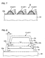
- Fig. 7 is a cross-sectional view of a principal part taken along the line B - B shown in Fig. 1 of the IDT electrode 31 included in the surface acoustic wave element 3 according to still another embodiment.
- Fig. 8 is an enlarged sectional view of one electrode finger 31a in the IDT electrode 31.
- the surface acoustic wave element 3 has an electrode finger 31a having a plurality of conductor layers laminated therein provided on a main surface 30a of a piezoelectric substrate 30 as the IDT electrode 31.
- the electrode finger 31a is covered with a protective film 34.
- the electrode finger 31a has two conductor layers, i.e., an intermediate layer 32 formed on the main surface 30a of the piezoelectric substrate 30 and an electrode layer 33 formed on the intermediate layer 32 laminated therein, as shown in Fig. 7 .
- Each of the intermediate layer 32 and the electrode layer 33 included in the electrode finger 31a is so formed that its cross section through a plane perpendicular to the longitudinal direction of the electrode finger 31a widens nearer to the main surface 30a of the piezoelectric substrate 30, as shown in Fig. 7 . That is, each of the intermediate layer 32 and the electrode layer 33 has a trapezoidal shape in the cross section.
- a lower surface of the electrode layer 33 in the electrode finger 31a, i.e., a joint surface 32a to the intermediate layer 32 does not extend out the joint surface 32a of the intermediate layer 32 but is included in the joint surface 32a of the intermediate layer 32.
- the width L 1 in a cross section of the joint surface 32a on which the intermediate layer 32 is opposed to the electrode layer 33 is formed larger than the width L 2 of a cross section of the joint surface 33a on which the electrode layer 33 is opposed to the intermediate layer 32, as shown in Fig. 8 .
- the electrode finger 31a has steps 32b on left and right having an L-shaped longitudinal cross-section and having a width R 3 as areas where the protective film 34 can be directly formed on the joint surface 32a of the intermediate layer 32 between a side surface of the intermediate layer 32 and a side surface of the electrode layer 33.
- the protective film 34 is directly formed on the joint surface 32a of the intermediate layer 32.
- the width L 1 in the cross section of the joint surface on which the intermediate layer is opposed to the electrode layer can be made larger than the width L 2 in the cross section of the joint surface on which the electrode layer is opposed to the intermediate layer by extending an etching time period longer to over-etch when the electrode finger is etched, for example.
- the two conductor layers forming the electrode finger 31a are formed such that an angle ⁇ 3 (e.g., 65°) formed between the side surface of the intermediate layer 32 and the main surface 30a of the piezoelectric substrate 30 is larger than an angle ⁇ 3 (e.g., 58°) formed between the side surface of the electrode layer 33 and the main surface 30a of the piezoelectric substrate 30 ( ⁇ 3 > ⁇ 3 ), as shown in Fig. 8 .
- ⁇ 3 e.g., 65°
- ⁇ 3 e.g., 58°
- the protective film 34 is formed of a material having a lower coefficient of thermal expansion than the largest coefficient of thermal expansion ( ⁇ 33 in this case) out of the respective coefficients of thermal expansion ⁇ 32 and ⁇ 33 of the conductor layers (the intermediate layer 32 and the electrode layer 33) forming the IDT electrode 31. This causes an extension due to thermal expansion of the electrode layer 33 is restrained by the protective film 34 on the step 32b. Accordingly, the shear stress created in the boundary between the intermediate layer 32 and the electrode layer 33 can be further restrained. Further, the adhesive properties of the protective film 34 can be improved.
- Fig. 9 is a cross-sectional view of a principal part taken along the line B - B shown in Fig. 1 of the IDT electrode 41 according to a further embodiment.
- Fig. 10 is an enlarged sectional view of one electrode finger 41a in the IDT electrode 41.
- the surface acoustic wave element 4 has an electrode finger 41a having a plurality of conductor layers laminated therein provided on a main surface 40a of a piezoelectric substrate 40 as the IDT electrode 41.
- the electrode finger 41a is covered with a protective film 44.
- the electrode finger 41a has a total of four conductor layers, i.e., an intermediate layer 42 formed on the main surface 40a of the piezoelectric substrate 40 and electrode layer 43 formed thereon that comprise two conductor layers, and another intermediate layer 42 and another electrode layer 43 that comprise two conductor layers, are laminated alternately, as shown in Fig. 9 .
- Each of the intermediate layer 42 and the electrode layer 43 included in the electrode finger 41a is so formed that its cross section through a plane perpendicular to the longitudinal direction of the electrode finger 41a widens nearer to the main surface 40a of the piezoelectric substrate 40. That is, each of the intermediate layer 42 and the electrode layer 43 has a trapezoidal shape.
- the width in a cross section of a joint surface 42a on which the intermediate layer 42 is opposed to the electrode layer 43 in the electrode finger 41a is formed larger than the width in a cross section of a joint surface 43a on which the electrode layer 43 is opposed to the intermediate layer 42, as shown in Fig. 10 . Therefore, the electrode finger 41a has steps 42b on left and right having an L-shaped longitudinal cross-section and having a width R 4 as areas where the protective film 44 can be directly formed on the joint surface 42a of the intermediate layer 42 between a side surface of the intermediate layer 42 and a side surface of the electrode layer 43.
- the width in the cross section of the joint surface on which the intermediate layer is opposed to the electrode layer can be made larger than the width in the cross section of the joint surface on which the electrode layer is opposed to the intermediate layer by extending an etching time period longer to over-etch when the electrode finger is etched, for example.
- the plurality of conductor layers forming the electrode finger 41a are formed such that an angle ⁇ 4 (e.g., 74°) formed between the side surface of the intermediate layer 42 and the main surface 40a of the piezoelectric substrate 40 is larger than an angle ⁇ 4 (e.g., 60°) formed between the side surface of the electrode layer 43 and the main surface 40a of the piezoelectric substrate 40 ( ⁇ 4 > ⁇ 4 ), as shown in Fig. 10 .
- an angle ⁇ 4 e.g., 74°
- ⁇ 4 e.g. 60°
- the protective film 44 is formed of a material having a lower coefficient of thermal expansion than the largest coefficient of thermal expansion ( ⁇ 43 in this case) out of the respective coefficients of thermal expansion ⁇ 42 and ⁇ 43 of the conductor layers 42 and 43 forming the IDT electrode 41.
- the angle ⁇ 4 with the side surface of the intermediate layer 42 is formed larger than the angle ⁇ 4 with the side surface of the electrode layer 43, as described above, a difference in a shear stress created in the electrode finger 41a between the conductor layers can be reduced, as compared with that in a case where the respective angles with the side surfaces of the conductor layers are the same.
- the width in the cross section of the joint surface 43a of the electrode layer 43 is formed smaller than the width in the cross section of the joint surface 42a of the intermediate layer 42, so that the protective film 44 laminated on the step 42b can restrain an extension due to thermal expansion of the electrode layer 43. This allows to relax a shear stress created in the boundary between the intermediate layer 42 and the electrode layer 43. As a result, the protective film 44 can be prevented from being fractured and stripped.
- the protective film 44 is directly formed on the joint surface 42a of the intermediate layer 42. Therefore, the extension of the electrode layer 43 having the larger coefficient of thermal expansion ⁇ 43 than that of the intermediate layer 42 in a direction toward the main surface 40a of the piezoelectric substrate 40 can be restrained.
- the electrode finger 41a is formed by three or more conductor layers, so that the durability of the electrode finger 41a can be further improved.
- an insulation protective film 14b can be further formed on an upper surface of a conductor protective film of an electrode finger 11a, or an insulation protective film 14b can be formed in place of the conductor protective film, as shown in Fig. 11 .
- This allows to enhance adhesive properties between the electrode finger 11a and a piezoelectric substrate 10 while protecting the IDT electrode 11.
- the insulation protective film 14b may be also formed on a main surface of the piezoelectric substrate 10. It goes without saying that insulation protective films are also formed on the IDT electrodes 21, 31, and 41 in the surface acoustic wave elements 2, 3, and 4, respectively.
- a surface acoustic wave element 1 shown in Figs. 3 and 4 was manufactured.
- a substrate formed of a LiTaO 3 single crystal as a material having piezoelectric properties was used as a piezoelectric substrate 10.
- Ti was deposited as an intermediate layer 12 on the piezoelectric substrate 10 using a sputtering method, and an Al-Cu (Cu: 1 % by weight) alloy having Cu contained in Al was deposited as an electrode layer 13 on the intermediate layer 12.
- the film thicknesses of Ti and an Al-Cu alloy were respectively 18 nm and 402 nm.
- An IDT electrode 11 and a reflector 19 were formed by patterning their shapes using a photolithographic technique, followed by a dry etching method.
- the etching conditions such as gas flow rate, pressure, applied power, and time were adjusted to control a side etching amount depending on a difference in etching rates between Ti and an Al-Cu alloy to adjust angles of inclination ⁇ 1 and ⁇ 1 .
- an RIE apparatus used was an ICP (Inductive Coupled Plasma)-RIE apparatus, the etching conditions were a BCl 3 gas flow rate of 20 sccm, a Cl 2 gas flow rate of 20 sccm, a N 2 gas flow rate of 10 sccm, a pressure of 1.0 Pa, a bias power of 60 W, and an etching time period required for processing of approximately 60 seconds.
- ICP Inductive Coupled Plasma
- an angle ⁇ 1 with the side surface of the intermediate layer 12 was 65° and an angle ⁇ 1 with the side surface of the electrode layer 13 was 58° when the main surface 10a of the piezoelectric substrate 10 was used as a reference.
- a metal layer (Ti) serving as a protective film 14 was then formed by a sputtering method using a mask used at the time of the dry etching.
- a surface acoustic wave element 2 shown in Figs. 5 and 6 was manufactured.
- a substrate formed of a LiTaO 3 single crystal as a material having piezoelectric properties was used as a piezoelectric substrate 20.
- Al-Cu (Cu: 1% by weight) alloy was first deposited as an intermediate layer 22 on the piezoelectric substrate 20 using a sputtering method, and Ti was deposited as an electrode layer 23 on the intermediate layer 22.
- the film thicknesses of Al-Cu and an Al-Cu alloy were 402 nm and 18 nm, respectively.
- An IDT electrode 21 and a reflector (not shown) were formed by patterning their shapes using a photolithographic technique, followed by a dry etching method. At this time, an etching selection ratio of the intermediate layer 22 and the electrode layer 23 was adjusted. Further, an angle formed between a side surface of each of conductor layers included in an electrode finger 21a and a main surface 20a of the piezoelectric substrate 20 was adjusted to be a designed angle using the dry etching method.
- the etching conditions were a BCl 3 gas flow rate of 20 sccm, a Cl 2 gas flow rate of 20 sccm, a N 2 gas flow rate of 20 sccm, a pressure of 1.0 Pa, a bias power of 60 W, and an etching time period required for processing of approximately 60 seconds.
- an angle ⁇ 2 with the side surface of the intermediate layer 22 was 60° and an angle ⁇ 2 with the side surface of the electrode layer 23 was 75° when the main surface 20a of the piezoelectric substrate 20 was used as a reference.
- a protective film 24 was formed of SiO 2 using a sputtering method. An unnecessary portion of the protective film 34 was trimmed by the dry etching method.
- a surface acoustic wave element 3 shown in Figs. 7 and 8 was manufactured.
- a substrate formed of an LiTaO 3 single crystal as a material having piezoelectric properties was used as a piezoelectric substrate 30.
- Ti was then deposited as an intermediate layer 32 on the piezoelectric substrate 30 using a sputtering method, and an Al-Cu (Cu: 1% by weight) alloy was deposited as an electrode layer 33 on the intermediate layer 32.
- the film thicknesses of Ti and an Al-Cu alloy were 18 nm and 402 nm, respectively.
- An IDT electrode 31 and a reflector were formed by patterning their respective shapes using a photolithographic technique, followed by a dry etching method.
- Cl 2 , BCl 3 and N 2 were used as reaction gas, and etching conditions such as gas flow rate, pressure, and applied power were adjusted to adjust an etching selection ratio of the intermediate layer 32 and the electrode layer 33.
- etching conditions such as gas flow rate, pressure, and applied power were adjusted to adjust an etching selection ratio of the intermediate layer 32 and the electrode layer 33.
- an angle formed between a side surface of each of conductor layers included in an electrode finger 31a and a main surface 30a of the piezoelectric substrate 30 was adjusted to be a designed angle using the dry etching method.
- the etching conditions were a BCl 3 gas flow rate of 20 sccm, a Cl 2 gas flow rate of 20 sccm, a N 2 gas flow rate of 10 sccm, a pressure of 1.0 Pa, a bias power of 60 W, and an etching time period required for processing of approximately 70 seconds.
- an angle ⁇ 3 with the side surface of the intermediate layer 32 was 65° and an angle ⁇ 3 with the side surface of the electrode layer 33 was 58° when the main surface 30a of the piezoelectric substrate 30 was used as a reference.
- the width in a cross section of a joint surface 33a of the electrode layer 33 was smaller by 8 nm on each of the left and right sides than the width in a cross section of a joint surface 32a of the intermediate layer 32 (see R 3 in Fig. 8 ) by overetching.
- the intermediate layer 32 and the electrode layer 33 were formed, followed by patterning using photolithography, and a protective film 34 was formed of SiO 2 using sputtering. An unnecessary portion of the protective film 34 was trimmed by the dry etching method.
- a surface acoustic wave element 4 shown in Figs. 9 and 10 was manufactured.
- a substrate formed of a LiTaO 3 single crystal as a material having piezoelectric properties was used as a piezoelectric substrate 40.
- Ti serving as an intermediate layer 42 was first deposited on the piezoelectric substrate 40 using a sputtering method, and an Al-Cu (Cu: 1% by weight) alloy serving as an electrode layer 43 was deposited on the intermediate layer 42.
- an Al-Cu (Cu: 1% by weight) alloy serving as an electrode layer 43 was deposited on the intermediate layer 42.
- two intermediate layers 42 and two electrode layers 43, or four layers are alternately laminated on a main surface 40a of the piezoelectric substrate 40.
- the film thicknesses of Ti and an Al-Cu alloy were 6 nm and 130 nm per layer, respectively.
- An IDT electrode 41 and a reflector were formed by patterning their shapes using a photolithographic technique, followed by a dry etching method.
- Cl 2 , BCl 3 and N 2 were used as reaction gas, and etching conditions such as gas flow rate, pressure, and applied power were adjusted to adjust an etching selection ratio of the intermediate layer 42 and the electrode layer 43.
- etching conditions such as gas flow rate, pressure, and applied power were adjusted to adjust an etching selection ratio of the intermediate layer 42 and the electrode layer 43.
- an angle formed between a side surface of each of conductor layers included in an electrode finger 41a and a main surface 40a of the piezoelectric substrate 40 was adjusted to be a designed angle using the dry etching method.
- the etching conditions were a BCl 3 gas flow rate of 20 sccm, a Cl 2 gas flow rate of 20 sccm, a N 2 gas flow rate of 10 sccm, a pressure of 1.0 Pa, a bias power of 60 W, and an etching time period required for processing of approximately 60 seconds.
- an angle ⁇ 4 with the side surface of the intermediate layer 42 was 74° and an angle ⁇ 4 with the side surface of the electrode layer 43 was 60° when the main surface 40a of the piezoelectric substrate 40 was used as a reference.
- the width in a cross section of a joint surface 42a of the intermediate layer 42 was larger by 16 nm on each of the left and right sides than the width in a cross section of a joint surface 43a of the electrode layer 43 (see R 4 in Fig. 10 ).
- the intermediate layer 42 and the electrode layer 43 were formed, followed by patterning using photolithography, and a protective film 44 was formed of SiO 2 using sputtering. After the protective film 44 was formed, an IDT electrode 41 was formed by the dry etching method.
Landscapes
- Physics & Mathematics (AREA)
- Acoustics & Sound (AREA)
- Surface Acoustic Wave Elements And Circuit Networks Thereof (AREA)
Abstract
Description
- The present invention relates to a surface acoustic wave element having an IDT electrode formed on a piezoelectric substrate, and a surface acoustic wave device carrying the same.
- Surface acoustic wave elements in which inter digital transducer (hereinafter merely referred to as IDT) electrodes are formed on piezoelectric substrates have been conventionally known. The IDT electrode can mutually convert an electrical signal and a surface acoustic wave. In addition to the IDT electrode, the surface acoustic wave element can confine energy by arranging reflector electrodes at positions between which the IDT electrode is sandwiched and multiple-reflecting the surface acoustic wave excited by the IDT electrode using the reflector electrodes on both sides thereof.
- In a duplexer used for a mobile terminal device such as a portable telephone, a surface acoustic wave device carrying a surface acoustic wave element having a high performance and capable of reducing size and weight has been used in recent years although a dielectric filter was conventionally used in principle. The input power level of the surface acoustic wave device has widened from a 10 mW level for an inter-stage filter in the mobile terminal device to 1 to 3 W levels required for the duplexer in the mobile terminal device with the spread of an application range of the surface acoustic wave device. In the surface acoustic wave device used in the duplexer for the mobile terminal device, therefore, the requirement of the input power level has increased with the rise in a working frequency band.
- On the other hand, in recent years, the operating frequency of the surface acoustic wave element has increased from several hundred megahertz to several gigahertzes. The line width of the IDT electrode included in the surface acoustic wave element has decreased with the increase in the operating frequency in inverse proportion to the frequency. Specifically, the line width of the IDT electrode is approximately 1 µm in an 800 MHz band, while being approximately 0.5 µm in a 1.9 GHz band. Therefore, an electrode finger formed in a comb shape in the IDT electrode requires fine processing with the increase in a frequency band.
- The line width of the IDT electrode reduces, and the input power level of the surface acoustic wave element included in the duplexer increases, as described above, so that the power-resistant life of the surface acoustic wave element in the GHz band decreases by two or more figures than the surface acoustic wave device in the 800 MHz band.
- In a case where the surface acoustic wave is excited and received using the fine electrode finger in the IDT electrode corresponding to the high frequency, when signal power applied to the surface acoustic wave device increases, a main surface of a piezoelectric substrate is distorted by the surface acoustic wave at the time of driving the surface acoustic wave device, so that an internal stress is created in the electrode finger in the IDT electrode. This internal stress causes a stress migration phenomenon to appear in the electrode finger. Therefore, the electrode finger is destroyed, and the IDT electrode is degraded.
- In addition thereto, in order to relax the internal stress, an Al atom within the electrode finger formed of Al (aluminum) migrates. As a result, holes are accumulated in an Al grain boundary, so that a void and a hillock are produced. In the surface acoustic wave device, therefore, there arises characteristic degradation of performance such as propagation or resonance of the surface acoustic wave and destruction of the electrode finger.
- Consequently, the surface acoustic wave element including the IDT electrode further requires durability against application of high power as applications are diversified. Therefore, an IDT electrode having an electrode finger whose durability is increased by laminating different materials has been developed in place of a conventional IDT electrode having an electrode finger formed of a single layer of a metal material such as Al or an Al alloy.
- For example, in Japanese Unexamined Patent Publication No.
2001-217672 intermediate layer 112 formed of a material such as Ti (titanium) is arranged between anAl electrode layer 113 and apiezoelectric substrate 110, and is covered with a protective film (metal film) 114 for the purpose of restraining the occurrence of stress migrations in theIDT electrode 111, as shown inFig. 13 in the present application. - Japanese Unexamined Patent Publication No.
2001-168671 - Japanese Unexamined Patent Publication No.
3-217109 - International Publication No.
WO2003/058813A1 discloses a structure of an IDT electrode formed by laminating a first metal layer having a trapezoidal cross section and a second metal layer having a rectangular cross section. - In the structure of the
IDT electrode 111 in Japanese Unexamined Patent Publication No.2001-217672 intermediate layer 12 and theelectrode layer 113 are formed almost perpendicular to themain surface 110a of thepiezoelectric substrate 110. In this case, when theprotective film 114 is formed by a film deposition method by which few evaporated species enter a masked area, such as an evaporation method, a material forming theprotective film 114 is incident from a direction substantially perpendicular to themain surface 110a of thepiezoelectric substrate 110, so that theprotective film 114 is formed thin on a side surface of theelectrode finger 111a. Therefore, theprotective film 114 degrades coverage on the side surface of theelectrode finger 111a. As a result, stress migrations such as fracture and stripping may occur. - Although Japanese Unexamined Patent Publication No.
2001-168671 - Japanese Unexamined Patent Publication No.
3-217109 - In International Publication No.
WO2003/058813A1 , when a shear stress arises on a boundary surface between two types of electrode layers because the electrode layers differ in coefficients of thermal expansion, each of the electrode layers cannot be prevented from being fractured and stripped, as in Japanese Unexamined Patent Publication No.2001-168671 - An object of the present invention is to provide a surface acoustic wave element whose durability can be enhanced by comprising an IDT electrode serving as an electrode finger having a plurality of conductor layers laminated therein while being capable of restraining the fracture and the stripping, for example., of the conductor layers and a surface acoustic wave device carrying the same.
- According to a surface acoustic wave element in the present invention, an electrode finger is formed by laminating a plurality of conductor layers including a first conductor layer and a second conductor layer formed of a material different from a material forming the first conductor layer. The first conductor layer has a trapezoidal shape that widens nearer to a piezoelectric substrate in cross section through a plane perpendicular to the longitudinal direction of the electrode finger, and the second conductor layer has a trapezoidal shape that widens nearer to the piezoelectric substrate in a cross section through a plane perpendicular to the longitudinal direction of the electrode finger. An angle formed between a side surface of the first conductor layer and a main surface of the piezoelectric substrate differs from an angle formed between a side surface of the second conductor layer and the main surface of the piezoelectric substrate.
- According to this configuration, the electrode finger has the two conductor layers laminated therein and is formed by the first conductor layer (intermediate layer) formed on the main surface of the piezoelectric substrate and the second conductor layer (electrode layer) formed on the first conductor layer. Each of the fist conductor layer and the second conductor layer included in the electrode finger is so formed that the cross section through the plane perpendicular to the longitudinal direction of the electrode finger widens nearer to the main surface of the piezoelectric substrate. That is, each of the first conductor layer and the second conductor layer has a trapezoidal shape.
- Since each of the conductor layers can have trapezoidal shapes having different angles of inclination, the fracture and the stripping, for example, of the protective film can be further restrained even if the materials forming the conductor layers differ in properties (e.g., coefficients of thermal expansion). This allows to restrain the fracture and the stripping of the protective film satisfactorily while forming the electrode finger by the plurality of conductor layers, thereby allowing to enhance the durability of the surface acoustic wave element.
- Although description is made using the example of the electrode finger having the two conductor layers laminated therein, the present invention is also satisfactorily applicable to an electrode finger having three or more conductor layers laminated therein.
- When the second conductor layer is formed of a material having a higher coefficient of thermal expansion than the material forming the first conductor layer, it is preferable that the angle formed between the side surface of the first conductor layer and the main surface of the piezoelectric substrate is formed larger than the angle formed between the side surface of the second conductor layer and the main surface of the piezoelectric substrate.
- According to this configuration, the coefficient of thermal expansion of the first conductor layer is lower than the coefficient of thermal expansion of the second conductor layer, so that a width of thermal expansion occurring in the first conductor layer is smaller than the width of thermal expansion occurring in the second conductor layer. The "width of thermal expansion" herein represents a width of extension in a direction substantially perpendicular to the side surface of each of the conductor layers. In addition thereto, the angle with the side surface of the first conductor layer is formed larger than the angle with the side surface of the second conductor layer, so that a shear stress due to a difference in the width of thermal expansion between the conductor layers forming the electrode finger can be relaxed. Accordingly, a difference between the extensions in a direction along the main surface of the piezoelectric substrate by the widths of thermal expansion in the conductor layers can be reduced, as compared with that in a case where the respective angles with the side surfaces of the conductor layers are the same.
- When the second conductor layer is formed of a material having a lower coefficient of thermal expansion than the material forming the first conductor layer, the angle formed between the side surface of the first conductor layer and the main surface of the piezoelectric substrate can be formed smaller than the angle formed between the side surface of the second conductor layer and the main surface of the piezoelectric substrate. This allows to restrain the fracture and the stripping, for example, of the protective film covering the surface of the electrode finger satisfactorily while forming the electrode finger by the plurality of conductor layers, thereby allowing to enhance the durability of the surface acoustic wave element.
- It is preferable that the first conductor layer is formed in contact with the main surface of the piezoelectric substrate, the second conductor layer is formed on the first conductor layer, and the width of the cross section opposed to the second conductor layer of the first conductor layer is formed larger than the width of the cross section opposed to the first conductor layer of the second conductor layer. According to this configuration, a joint surface of the second conductor layer is formed smaller than a joint surface of the first conductor layer, so that the protective film can be laminated in an area (a step) from the side surface of the first conductor layer to the side surface of the second conductor layer on the first conductor layer. Accordingly, the extension due to the thermal expansion in the second conductor layer is restrained by the protective film on the first conductor layer. Therefore, a shear stress created in the boundary between the first conductor layer and the second conductor layer can be further restrained.
- The electrode finger in the IDT electrode may be covered with a protective film. This can prevent each of the conductor layers forming the electrode finger from being stripped.
- It is preferable that the protective film is formed of a material having a lower coefficient of thermal expansion than one having the largest coefficient of thermal expansion among the conductor layers forming the electrode finger. Accordingly, the protective film can restrain the extensions due to the thermal expansion in the first conductor layer and the second conductor layer.
- The protective film may be formed only on the IDT electrode, and may contain at least one of Ti, Cr, Nb, Pd, Cu, and Ni as a material.
- A surface acoustic wave device according to the present invention is so adapted that the above-mentioned surface acoustic wave element is mounted on a mounting substrate, and has an IDT electrode having high reliability, as described above. Thus, a longer life can be expected for the surface acoustic wave device.
- As described in the foregoing, according to the present invention, the shear stress created in the electrode finger in the IDT electrode can be relaxed. This allows to improve the temperature characteristics of the surface acoustic wave element. Further, the production of a hillock and a void due to stress migrations can be restrained. Therefore, it is less likely to destroy the IDT electrode against high input power, thereby allowing to improve the durability of the surface acoustic wave element.
- The foregoing and other objects, features, aspects and advantages of the present invention will become more apparent from the following detailed description of the present invention when taken in conjunction with the accompanying drawings.
-
-
Fig. 1 is a plan view of a surface acoustic wave element according to an embodiment of the present invention. -
Fig. 2 is a cross-sectional view taken along a line A - A showing a state where a surface acoustic wave element is mounted on a mounting substrate. -
Fig. 3 is a cross-sectional view of a principal part taken along a line B - B shown inFig. 1 of an IDT electrode included in a surfaceacoustic wave element 1. -
Fig. 4 is an enlarged sectional view of one electrode finger in the IDT electrode. -
Fig. 5 is a cross-sectional view of a principal part taken along a line B - B shown inFig. 1 of an IDT electrode included in a surface acoustic wave element 2 according to another embodiment. -
Fig. 6 is an enlarged sectional view of one electrode finger in the IDT electrode. -
Fig. 7 is a cross-sectional view of a principal part taken along a line B - B shown inFig. 1 of an IDT electrode included in a surface acoustic wave element 3 according to still another embodiment. -
Fig. 8 is an enlarged sectional view of one electrode finger in the IDT electrode. -
Fig. 9 is a cross-sectional view of a principal part taken along a line B - B shown inFig. 1 of an IDT electrode included in a surface acoustic wave element 4 according to a still further embodiment. -
Fig. 10 is an enlarged sectional view of one electrode finger in the IDT electrode. -
Fig. 11 is an enlarged sectional view showing a state where an insulation protective film is formed on an electrode finger in an IDT electrode included in a surfaceacoustic wave element 1. -
Fig. 12 is a plan view of a surface acoustic wave element according to a still further embodiment of the present invention. -
Fig. 13 is an enlarged sectional view of an electrode finger in a conventional IDT electrode. -
Fig. 1 is a plan view of a ladder-type surface acoustic wave element according to an embodiment of the present invention.Fig. 2 is a cross-sectional view taken along a line A - A in a case where the surface acoustic wave element is mounted on a mounting substrate. - A surface
acoustic wave element 1 has apiezoelectric substrate 10, and anIDT electrode 11 formed on amain surface 10a of thepiezoelectric substrate 10. Here, "themain surface 10a of thepiezoelectric substrate 10" refers to a surface on which theIDT electrode 11 is formed in the plate-shapedpiezoelectric substrate 10. - The surface
acoustic wave element 1 comprises reflector electrodes (hereinafter also referred to as reflectors) 19 having a slit shape at positions between which theIDT electrode 11 is sandwiched in the direction of signal propagation of the IDT electrode 11 (in a top-and-bottom direction on a paper surface). Thereflector 19 can multi-reflect a surface acoustic wave excited in theIDT electrode 11 and can configure energy of the generated surface acoustic wave. - In the surface
acoustic wave element 1, anannular electrode 16 is formed at a position enclosing theIDT electrode 11 and thereflector 19 on themain surface 10a of thepiezoelectric substrate 10. In addition thereto, awiring electrode pad 18 connected to theIDT electrode 11 through a pull-outelectrode 17 is formed on the surfaceacoustic wave element 1. - The surface
acoustic wave element 1 is placed and fixed on the mountingsubstrate 90 made of resin using a so-called face-down system with themain surface 10a having theIDT electrode 11 formed thereon opposed to an upper surface of the mountingsubstrate 90. Theannular electrode 16 is joined to an annular conductor opposed thereto on the mountingsubstrate 90 through a jointing material such as solder to join thewiring electrode pad 18 to a wiring conductor opposed thereto on the mountingsubstrate 90 as shown inFig. 2 that is a cross-sectional view. The joint surfaces are joined to each other by subjecting the jointing material to reflow melting. The reflow melting forms anannular electrode portion 91 having theannular electrode 16 and the annular conductor jointed to each other, and awiring electrode portion 92 having thewiring electrode pad 18 and the wiring conductor joined to each other. - In such a way, the surface
acoustic wave element 1 is placed and fixed on the mountingsubstrate 90 and is flip-chip mounted thereon, thereby manufacturing a surface acoustic wave device S configured by electrically and mechanically connecting the surfaceacoustic wave element 1 to the mountingsubstrate 90. - The
piezoelectric substrate 10 is formed of a material having piezoelectric properties such as a 38.7° Y-cut X-propagation LiTaO3 single crystal, a 64° Y-cut X-propagation LiNbO3 single crystal, a 45° X-cut Z-propagation LiB4O7 single crystal, or the like. This allows to increase the electromechanical coupling coefficient and to decrease the group delay time temperature coefficient of thepiezoelectric substrate 10, respectively. - The thickness of the
piezoelectric substrate 10 is preferably 0.15 to 0.5 mm. In a case where the thickness is less than 0.15 mm, thepiezoelectric substrate 10 is brittle and is damaged easily. In contrast, in a case where the thickness is 0.5 mm, the material cost is increased. - The
IDT electrode 11 formed on themain surface 10a of thepiezoelectric substrate 10 has a pair ofelectrode fingers 11a formed in such a comb shape that they are interdigitated with each other, as shown inFig. 1 . - The number of
electrode fingers 11a on each side is preferably 50 to 200. The width of each of theelectrode fingers 11a is 0.1 to 10 µm. A clearance (pitch) between theadjacent electrode fingers 11a is 0.1 to 10 µm. A length (cross width) in which the opposedelectrode fingers 11a are interdigitated with each other is 10 to 300 µm. TheIDT electrode 11 has a height (thickness) of 0.1 to 0.6 µm in order to satisfactorily obtain prescribed characteristics as a surface acoustic wave resonator and a surface acoustic wave filter. - The
IDT electrode 11 is formed by an electrode layer composed of an Al alloy like Al-Cu or the like and a Ti intermediate layer, as described later, using a thin film deposition method such as a sputtering method, evaporation method, or a CVD (Chemical Vapor Deposition) method. - A metal added to Al as the above-mentioned Al alloy is Cu. In some cases, metals such as Ti, Ta, W, Mo, and Mg may be used together with or in place of Cu. The
IDT electrode 11 has a predetermined shape by patterning using a photolithographic method. - The above-mentioned materials forming the
IDT electrode 11 are also applicable to thereflector 19 having such a slit shape that a plurality of electrode fingers are arranged parallel to one another. - Although the ladder-type surface acoustic wave filter is illustrated as the surface
acoustic wave element 1 inFig. 1 , the surfaceacoustic wave element 1 may be composed of a DMS-type surface acoustic wave resonator filter shown inFig. 12 . - The DMS-type surface acoustic wave resonator filter shown in
Fig. 12 has a piezoelectric substrate 10' and IDT electrodes 11' formed on amain surface 10a' of the piezoelectric substrate 10', similarly to the ladder-type surfaceacoustic wave element 1 shown inFig. 1 . The IDT electrodes 11' are coupled to each other through a pull-out wire 17'. The surface acoustic wave element 1' comprises reflectors 19' at positions between which the IDT electrodes 11' are sandwiched in the direction of signal propagation in the IDT electrodes 11' (in a left-and-right direction on a paper surface). In the surface acoustic wave element 1', an annular electrode 16' is formed at a position enclosing the IDT electrodes 11' and the reflectors 19' of themain surface 10a' of the piezoelectric substrate 10'. In addition thereto, wiring electrode pads 18' each connected to the IDT electrodes 11' through the pull-out wires 17' are formed in the surface acoustic wave element 1'. - Although description is now made to the structure of the IDT electrode on the basis of the ladder-type surface
acoustic wave element 1 shown inFig. 1 , it should be noted that the structure of the IDT electrode 11' in the DMS-type surface acoustic wave resonator filter shown inFig. 12 is the same. -
Fig. 3 is a cross-sectional view of a principal part taken along a line B - B shown inFig. 1 of theIDT electrode 11 included in the surfaceacoustic wave element 1.Fig. 4 is an enlarged sectional view of oneelectrode finger 11a in theIDT electrode 11. - The surface
acoustic wave element 1 has anelectrode finger 11a having a plurality of conductor layers laminated therein provided on themain surface 10a of thepiezoelectric substrate 10 as theIDT electrode 11. Theelectrode finger 11a is covered with aprotective film 14. - The
electrode finger 11a has two conductor layers, i.e., a first conductor layer (hereinafter also referred to as an intermediate layer) 12 formed on themain surface 10a of thepiezoelectric substrate 10 and a second conductor layer (hereinafter referred to as an electrode layer) 13 formed on theintermediate layer 12 laminated therein, as shown inFig. 3 . - Each of the
intermediate layer 12 and theelectrode layer 13 is so formed that its cross section through a plane perpendicular to the longitudinal direction of theelectrode finger 11a widens nearer to themain surface 10a of thepiezoelectric substrate 10, as shown inFig. 3 . That is, each of theintermediate layer 12 and theelectrode layer 13 has a trapezoidal shape in the cross section. - Even if a material forming the
protective film 14 is incident from a direction substantially perpendicular to themain surface 10a of thepiezoelectric substrate 10 using a film deposition method by which few evaporated species enter a masked area, theprotective film 14 can be formed in a sufficient thickness on a side surface of theelectrode finger 11a, so that the fracture and the stripping of theprotective film 14 can be restrained. - The
intermediate layer 12 is formed of a metal material such as Ti (let ρ12 be its coefficient of thermal expansion, ρ12=8/9×10-6/K). - The
electrode layer 13 is formed of a metal material such as an Al alloy having a higher coefficient of thermal expansion than that of the material forming theintermediate layer 12, e.g., an Al-Cu (Cu: 1 % by weight) alloy (let ρ13 be its coefficient of thermal expansion, ρ13=23.5×10⁻⁶/K). - Furthermore, the
electrode layer 13 can be formed of a metal material having a metal such as Ti, Ta, W, Mo, or Mg, described above, added thereto together with or in place of Cu as a material to be contained in Al serving as a main component. - The
electrode layer 13 and theintermediate layer 12 serving as two conductor layers included in theelectrode finger 11a are formed such that an angle α1 (e.g., 65°) formed between a side surface of theintermediate layer 12 and themain surface 10a of thepiezoelectric substrate 10 is larger than an angle β1 (e.g., 58°) formed between a side surface of theelectrode layer 13 and themain surface 10a of the piezoelectric substrate 10 (α1 > β1), as shown inFig. 4 . This allows to disperse a stress created in each of the conductor layers in theelectrode finger 11a (the details will be described later). - The angle with the side surface of each of the conductor layers in the
electrode finger 11a can be adjusted by etching, as described below. That is, the conductor layers in theelectrode finger 11a are laminated, and the shape of each conductor layer is patterned using a photolithographic technique, and a dry etching method thereafter. In the dry etching method, Cl2, BCl3 and N2 are used as reaction gas, and etching conditions such as gas flow rate, pressure, applied power, and time are adjusted to control a side etching amount (an etching amount on the side surface of each of the conductor layers) utilizing a difference in etching rates between Ti and an Al alloy. This allows to adjust the respective angles α1 and β1 with the side surfaces of the conductor layers (theintermediate layer 12 and the electrode layer 13) in theelectrode finger 11a. Specifically, it is effective to increase the gas concentration of BCl3 and increase power to apply in order to increase the side etching amount, i.e., reduce the angle formed between the side surface of the conductor layer and the main surface of the piezoelectric substrate. - The
protective film 14 is provided so as to protect theelectrode finger 11a. After theIDT electrode 11 is formed, theprotective film 14 is formed by forming a predetermined material on theIDT electrode 11 using a CVD method. Theprotective film 14 can be also formed using a method such as a sputtering method or an evaporation method in addition to the CVD method. - The
protective film 14 can use a conductor protective film formed of a material having conductive properties, a semiconductor film formed of a material having semiconductor properties, or an insulation protective film formed of a material having insulation properties. - Although description is herein made to a case where the conductor protective film is formed of Ti, it can be mainly composed of any of metal materials such as Cr, Nb, Pd, Cu, and Ni other than Ti. The conductor
protective film 14 is formed only on theelectrode finger 11a in theIDT electrode 11. - The insulation protective film is formed of a material having insulation properties such as silicon dioxide or silicon nitride. The semiconductor film is formed of a material having semiconductor properties such as polycrystalline silicon. At this time, the insulation protective film and the semiconductor film may be formed only on the
electrode finger 11a. Alternatively, they can be also formed on themain surface 10a of thepiezoelectric substrate 10 in addition to theelectrode finger 11a. - Description is now made to a mechanism for relaxing a shear stress created in each of the conductor layers based on the setting of the angles α1 and β1 in the surface
acoustic wave element 1. - In the vicinity of the side surface of each of the conductor layers (the
intermediate layer 12 and the electrode layer 13), a stress due to thermal expansion of the conductor layer is created outward in a direction substantially perpendicular to the side surface of the conductor layer. As shown inFig. 4 , an extension occurs by a width A1 of thermal expansion in the vicinity of the side surface of theintermediate layer 12, and an extension occurs by a width B1 of thermal expansion in the vicinity of the side surface of theelectrode layer 13. Here, "the width of thermal expansion" represents a width of extension in the direction substantially perpendicular to the side surface of each of the conductor layers, and is defined by the volume of the conductor layer, the width thereof in a plane direction, the coefficient of thermal expansion p thereof, and so on. - In this example, the coefficient of thermal expansion ρ12 of the
intermediate layer 12 is lower than the coefficient of thermal expansion ρ13 of theelectrode layer 13, so that the width A1 of thermal expansion is smaller than the width B1 of thermal expansion (A1 < B1). - Accordingly, the extension occurring in the direction along the
main surface 10a of thepiezoelectric substrate 10 by the width A1 of thermal expansion is A1sinα1 in theintermediate layer 12, and the extension occurring in the direction along themain surface 10a of thepiezoelectric substrate 10 by the width B1 of thermal expansion is B1sinβ1 in theelectrode layer 13. - Here, the angle α1 with the side surface of the
intermediate layer 12 is formed larger than the angle β1 with the side surface of the electrode layer 13 (sinα1 > sinβ1), so that a difference between the respective extensions (A1sinα1 and B1sinβ1) occurring in the direction along themain surface 10a of thepiezoelectric substrate 10 in the conductor layers can be reduced, as compared with that in a case where the respective angles with the side surfaces of the conductor layers are the same. - Consequently, the angle formed with the side surface of each of the conductor layers can be adjusted depending on the coefficient of thermal expansion of the conductor layer, so that a shear stress created on a boundary surface between the
intermediate layer 12 and theelectrode layer 13 can be relaxed. As a result, the fracture and the stripping of theprotective film 14 can be restrained. - It is preferable that the angle α1 formed with the side surface of the
intermediate layer 12 has an angle not exceeding 80°. If this angle takes a value in a range not exceeding 80°, theprotective film 14 can have a sufficient thickness up to a portion close to themain surface 10a of thepiezoelectric substrate 10 of the side surface of theelectrode finger 11a even when it is formed using a film deposition method by which few evaporated species enter a masked area, for example, evaporation, and thus has good adhesive properties to theintermediate layer 12 and theelectrode layer 13. - A difference between the angles (α1-β1) formed with the side surfaces of the
intermediate layer 12 and theelectrode layer 13 is preferably in a range of 10° to 20° and more preferably 15°. At this time, theprotective film 14 has good adhesive properties to theintermediate layer 12 and theelectrode layer 13. - A surface acoustic wave element according to another embodiment of the present invention will be described. Surface acoustic wave elements 2, 3, and 4 (including
piezoelectric substrates main surfaces IDT electrodes piezoelectric substrate 10, itsmain surface 10a, and the IDT electrode 11) shown inFig. 1 , and the surface acoustic wave element 1' (including the piezoelectric substrate 10', itsmain surface 10a', and the IDT electrode 11') shown inFig. 12 in portions that are not particularly referred to. -
Fig. 5 is a cross-sectional view of a principal part taken along the line B - B shown inFig. 1 of theIDT electrode 21 included in the surface acoustic wave element 2 according to another embodiment.Fig. 6 is an enlarged sectional view of oneelectrode finger 21a in theIDT electrode 21. - The surface acoustic wave element 2 has an
electrode finger 21a having a plurality of conductor layers laminated therein provided on amain surface 20a of apiezoelectric substrate 20 as theIDT electrode 21. Theelectrode finger 21a is covered with aprotective film 24. - The
electrode finger 21a has two conductor layers, i.e., anintermediate layer 22 serving as a first conductor layer formed on themain surface 20a of thepiezoelectric substrate 20 and anelectrode layer 23 serving as a second conductor layer formed on theintermediate layer 22 laminated therein, as shown inFig. 5 . Each of theintermediate layer 22 and theelectrode layer 23 included in theelectrode finger 21a is so formed that its cross section through a plane perpendicular to the longitudinal direction of theelectrode finger 21a widens nearer to themain surface 20a of thepiezoelectric substrate 20, as shown inFig. 5 . That is, each of theintermediate layer 22 and theelectrode layer 23 has a trapezoidal shape in the cross section. - The
intermediate layer 22 is formed of a metal material such as an Al alloy having a metal material such as Cu or Mg contained in Al, e.g., an Al-Cu (Cu: 1 % by weight) alloy (let ρ22 be its coefficient of thermal expansion, ρ22=23.5×10⁻⁶/K). - The
electrode layer 23 is formed of a metal material such as Ta having a lower coefficient of thermal expansion than that of the material forming the intermediate layer 22 (let ρ23 be the coefficient of thermal expansion, ρ23=6.6×10⁻⁶/K). - The two conductor layers forming the
electrode finger 21a are formed such that an angle α2 (e.g., 60°) formed between a side surface of theintermediate layer 22 and themain surface 20a of thepiezoelectric substrate 20 is smaller than an angle β2 (e.g., 75°) formed between a side surface of theelectrode layer 23 and themain surface 20a of the piezoelectric substrate 20 (α2 < β2), as shown inFig. 6 . - The
protective film 24 is provided so as to protect theelectrode finger 21a. After theIDT electrode 21 is formed, theprotective film 24 is formed by forming a predetermined material on theIDT electrode 21 using a CVD method, similarly to theprotective film 14. - An extension occurs by a width A2 of thermal expansion in the vicinity of the side surface of the
intermediate layer 22, and an extension occurs by a width B2 of thermal expansion in the vicinity of the side surface of theelectrode layer 23. At this time, the coefficient of thermal expansion ρ22 of theintermediate layer 22 is higher than the coefficient of thermal expansion ρ23 of theelectrode layer 23, so that the width A2 of thermal expansion is larger than the width B1 of thermal expansion (A2 > B2). - Accordingly, the extension occurring in the direction along the
main surface 20a of thepiezoelectric substrate 20 by the width A2 of thermal expansion is A2sinα2 in theintermediate layer 22, and the extension occurring in the direction along themain surface 20a of thepiezoelectric substrate 20 by the width B2 of thermal expansion is B2sinβ2 in theelectrode layer 23. The angle α2 with the side surface of theintermediate layer 22 is smaller than the angle β2 with the side surface of the electrode layer 23 (sinα2 < sinβ2), so that a difference between the respective extensions (A2sinα2 and B2sinβ2) occurring in the direction along themain surface 20a of thepiezoelectric substrate 20 in the conductor layers can be reduced, as compared with that in a case where the respective angles with the side surfaces of the conductor layers are the same. - Consequently, the angle formed with the side surface of each of the conductor layers can be adjusted depending on the coefficient of thermal expansion of the conductor layer, so that a shear stress created on a boundary surface between the
intermediate layer 22 and theelectrode layer 23 can be relaxed. As a result, theprotective film 24 can be prevented from being fractured and stripped. - It is preferable that the angle α2 formed with the side surface of the
intermediate layer 22 is an angle in a range of 45° to 80°. The angle is more preferably in a range of 60° to 80°. - The electrode pattern of a high-frequency filter is made finer, so that a small difference of mass on the
electrode finger 21a becomes important. The mass difference means a difference in mass between electrodes based on the shape of an electrode thin film on thepiezoelectric substrate 20. Here, the shape of theIDT electrode 21, i.e., the mass of theelectrode finger 21a forming theIDT electrode 21 affects the excitation of a surface acoustic wave. This is referred to as a "mass effect", and affects the frequency characteristics of the surface acoustic wave. A center frequency in the characteristics may be shifted from a desired value due to the mass (the shape, and particularly the line width and the film thickness) of the electrode thin film. If the angle α2 formed with the side surface of theintermediate layer 22 is an angle exceeding 45°, the above-mentioned mass effect can be reduced, and the design value of the frequency characteristics hardly greatly differs from the actually measured value thereof, so that a stable yield can be obtained. - A difference between the angles (α2-β2) formed with the side surfaces of the
intermediate layer 22 and theelectrode layer 23 is preferably in a range of 10° to 20°, and more preferably 15°. At this time, theprotective film 24 has good adhesive properties to theintermediate layer 22 and theelectrode layer 23. -
Fig. 7 is a cross-sectional view of a principal part taken along the line B - B shown inFig. 1 of theIDT electrode 31 included in the surface acoustic wave element 3 according to still another embodiment.Fig. 8 is an enlarged sectional view of oneelectrode finger 31a in theIDT electrode 31. - The surface acoustic wave element 3 has an
electrode finger 31a having a plurality of conductor layers laminated therein provided on amain surface 30a of apiezoelectric substrate 30 as theIDT electrode 31. Theelectrode finger 31a is covered with aprotective film 34. - The
electrode finger 31a has two conductor layers, i.e., anintermediate layer 32 formed on themain surface 30a of thepiezoelectric substrate 30 and anelectrode layer 33 formed on theintermediate layer 32 laminated therein, as shown inFig. 7 . - Each of the
intermediate layer 32 and theelectrode layer 33 included in theelectrode finger 31a is so formed that its cross section through a plane perpendicular to the longitudinal direction of theelectrode finger 31a widens nearer to themain surface 30a of thepiezoelectric substrate 30, as shown inFig. 7 . That is, each of theintermediate layer 32 and theelectrode layer 33 has a trapezoidal shape in the cross section. - A lower surface of the
electrode layer 33 in theelectrode finger 31a, i.e., ajoint surface 32a to theintermediate layer 32 does not extend out thejoint surface 32a of theintermediate layer 32 but is included in thejoint surface 32a of theintermediate layer 32. - The width L1 in a cross section of the
joint surface 32a on which theintermediate layer 32 is opposed to theelectrode layer 33 is formed larger than the width L2 of a cross section of thejoint surface 33a on which theelectrode layer 33 is opposed to theintermediate layer 32, as shown inFig. 8 . - Therefore, the
electrode finger 31a hassteps 32b on left and right having an L-shaped longitudinal cross-section and having a width R3 as areas where theprotective film 34 can be directly formed on thejoint surface 32a of theintermediate layer 32 between a side surface of theintermediate layer 32 and a side surface of theelectrode layer 33. In thestep 32b, theprotective film 34 is directly formed on thejoint surface 32a of theintermediate layer 32. The width L1 in the cross section of the joint surface on which the intermediate layer is opposed to the electrode layer can be made larger than the width L2 in the cross section of the joint surface on which the electrode layer is opposed to the intermediate layer by extending an etching time period longer to over-etch when the electrode finger is etched, for example. - The
intermediate layer 32 is formed of a metal material such as Ti (let ρ32 be its coefficient of thermal expansion, ρ32=8.9×10⁻⁶/K). - The
electrode layer 33 is formed of a metal material such as an Al alloy having a higher coefficient of thermal expansion than that of the material forming theintermediate layer 32, e.g., an Al-Cu (Cu: 1 % by weight) alloy (let ρ33 be its coefficient of thermal expansion, ρ33=23.5×10⁻⁶/K). - The two conductor layers forming the
electrode finger 31a are formed such that an angle α3 (e.g., 65°) formed between the side surface of theintermediate layer 32 and themain surface 30a of thepiezoelectric substrate 30 is larger than an angle β3 (e.g., 58°) formed between the side surface of theelectrode layer 33 and themain surface 30a of the piezoelectric substrate 30 (α3 > β3), as shown inFig. 8 . - Since the angle α3 with the side surface of the
intermediate layer 32 is formed larger than the angle β3 with the side surface of theelectrode layer 33, as described above, a difference in a shear stress created in theelectrode finger 31a between the conductor layers can be reduced, as compared with that in a case where the respective angles with the side surfaces of the conductor layers are the same. - This allows to relax a shear stress created on a boundary surface between the
intermediate layer 32 and theelectrode layer 33 by adjusting the angle formed with the side surface of each of the conductor layers depending on the coefficient of thermal expansion of the conductor layer. As a result, theprotective film 34 can be prevented from being fractured and stripped. - The
protective film 34 is formed of a material having a lower coefficient of thermal expansion than the largest coefficient of thermal expansion (ρ33 in this case) out of the respective coefficients of thermal expansion ρ32 and ρ33 of the conductor layers (theintermediate layer 32 and the electrode layer 33) forming theIDT electrode 31. This causes an extension due to thermal expansion of theelectrode layer 33 is restrained by theprotective film 34 on thestep 32b. Accordingly, the shear stress created in the boundary between theintermediate layer 32 and theelectrode layer 33 can be further restrained. Further, the adhesive properties of theprotective film 34 can be improved. -
Fig. 9 is a cross-sectional view of a principal part taken along the line B - B shown inFig. 1 of theIDT electrode 41 according to a further embodiment.Fig. 10 is an enlarged sectional view of oneelectrode finger 41a in theIDT electrode 41. - The surface acoustic wave element 4 has an
electrode finger 41a having a plurality of conductor layers laminated therein provided on amain surface 40a of apiezoelectric substrate 40 as theIDT electrode 41. Theelectrode finger 41a is covered with aprotective film 44. - The
electrode finger 41a has a total of four conductor layers, i.e., anintermediate layer 42 formed on themain surface 40a of thepiezoelectric substrate 40 andelectrode layer 43 formed thereon that comprise two conductor layers, and anotherintermediate layer 42 and anotherelectrode layer 43 that comprise two conductor layers, are laminated alternately, as shown inFig. 9 . - Each of the
intermediate layer 42 and theelectrode layer 43 included in theelectrode finger 41a is so formed that its cross section through a plane perpendicular to the longitudinal direction of theelectrode finger 41a widens nearer to themain surface 40a of thepiezoelectric substrate 40. That is, each of theintermediate layer 42 and theelectrode layer 43 has a trapezoidal shape. - The width in a cross section of a
joint surface 42a on which theintermediate layer 42 is opposed to theelectrode layer 43 in theelectrode finger 41a is formed larger than the width in a cross section of ajoint surface 43a on which theelectrode layer 43 is opposed to theintermediate layer 42, as shown inFig. 10 . Therefore, theelectrode finger 41a hassteps 42b on left and right having an L-shaped longitudinal cross-section and having a width R4 as areas where theprotective film 44 can be directly formed on thejoint surface 42a of theintermediate layer 42 between a side surface of theintermediate layer 42 and a side surface of theelectrode layer 43. The width in the cross section of the joint surface on which the intermediate layer is opposed to the electrode layer can be made larger than the width in the cross section of the joint surface on which the electrode layer is opposed to the intermediate layer by extending an etching time period longer to over-etch when the electrode finger is etched, for example. - The
intermediate layer 42 is formed of a metal material such as Ti (let ρ42 be its coefficient of thermal expansion, ρ42=8.9×10⁻⁶/K). - The
electrode layer 43 is formed of a metal material such as an Al alloy having a higher coefficient of thermal expansion than that of the material forming theintermediate layer 42, e.g., an Al-Cu (Cu: 1 % by weight) alloy (let ρ42 be its coefficient of thermal expansion, ρ42=23.5×10⁻⁶/K). - The plurality of conductor layers forming the
electrode finger 41a are formed such that an angle α4 (e.g., 74°) formed between the side surface of theintermediate layer 42 and themain surface 40a of thepiezoelectric substrate 40 is larger than an angle β4 (e.g., 60°) formed between the side surface of theelectrode layer 43 and themain surface 40a of the piezoelectric substrate 40 (α4 > β4), as shown inFig. 10 . - The
protective film 44 is formed of a material having a lower coefficient of thermal expansion than the largest coefficient of thermal expansion (ρ43 in this case) out of the respective coefficients of thermal expansion ρ42 and ρ43 of the conductor layers 42 and 43 forming theIDT electrode 41. - Since the angle α4 with the side surface of the
intermediate layer 42 is formed larger than the angle β4 with the side surface of theelectrode layer 43, as described above, a difference in a shear stress created in theelectrode finger 41a between the conductor layers can be reduced, as compared with that in a case where the respective angles with the side surfaces of the conductor layers are the same. In addition thereto, the width in the cross section of thejoint surface 43a of theelectrode layer 43 is formed smaller than the width in the cross section of thejoint surface 42a of theintermediate layer 42, so that theprotective film 44 laminated on thestep 42b can restrain an extension due to thermal expansion of theelectrode layer 43. This allows to relax a shear stress created in the boundary between theintermediate layer 42 and theelectrode layer 43. As a result, theprotective film 44 can be prevented from being fractured and stripped. - In the
step 42b, theprotective film 44 is directly formed on thejoint surface 42a of theintermediate layer 42. Therefore, the extension of theelectrode layer 43 having the larger coefficient of thermal expansion ρ43 than that of theintermediate layer 42 in a direction toward themain surface 40a of thepiezoelectric substrate 40 can be restrained. - In the present embodiment, the
electrode finger 41a is formed by three or more conductor layers, so that the durability of theelectrode finger 41a can be further improved. - Although description is made to the embodiment in which the conductor protective film is formed only on the IDT electrode in the above-mentioned surface
acoustic wave element 1, an insulationprotective film 14b can be further formed on an upper surface of a conductor protective film of anelectrode finger 11a, or an insulationprotective film 14b can be formed in place of the conductor protective film, as shown inFig. 11 . This allows to enhance adhesive properties between theelectrode finger 11a and apiezoelectric substrate 10 while protecting theIDT electrode 11. In a case where the insulationprotective film 14b is formed, the insulationprotective film 14b may be also formed on a main surface of thepiezoelectric substrate 10. It goes without saying that insulation protective films are also formed on theIDT electrodes - A surface
acoustic wave element 1 shown inFigs. 3 and 4 was manufactured. A substrate formed of a LiTaO3 single crystal as a material having piezoelectric properties was used as apiezoelectric substrate 10. - Ti was deposited as an
intermediate layer 12 on thepiezoelectric substrate 10 using a sputtering method, and an Al-Cu (Cu: 1 % by weight) alloy having Cu contained in Al was deposited as anelectrode layer 13 on theintermediate layer 12. The film thicknesses of Ti and an Al-Cu alloy were respectively 18 nm and 402 nm. - An
IDT electrode 11 and areflector 19 were formed by patterning their shapes using a photolithographic technique, followed by a dry etching method. - In the dry etching method, Cl2, BCl3 and N2 were used as reaction gas, and etching conditions such as gas flow rate, pressure, and applied power were adjusted to adjust an etching selection ratio of Ti and an Al-Cu alloy.
- That is, the etching conditions such as gas flow rate, pressure, applied power, and time were adjusted to control a side etching amount depending on a difference in etching rates between Ti and an Al-Cu alloy to adjust angles of inclination α1 and β1. Specifically, an RIE apparatus used was an ICP (Inductive Coupled Plasma)-RIE apparatus, the etching conditions were a BCl3 gas flow rate of 20 sccm, a Cl2 gas flow rate of 20 sccm, a N2 gas flow rate of 10 sccm, a pressure of 1.0 Pa, a bias power of 60 W, and an etching time period required for processing of approximately 60 seconds.
- As an angle with a side surface of an
electrode finger 11a at this time, an angle α1 with the side surface of theintermediate layer 12 was 65° and an angle β1 with the side surface of theelectrode layer 13 was 58° when themain surface 10a of thepiezoelectric substrate 10 was used as a reference. - After the
intermediate layer 12 and theelectrode layer 13 were formed, a metal layer (Ti) serving as aprotective film 14 was then formed by a sputtering method using a mask used at the time of the dry etching. - Even if a high frequency was applied to the surface
acoustic wave element 1 thus manufactured, or an ambient temperature was changed, theprotective film 14 was not stripped. High yields were obtained within a wafer surface and between wafers of the surfaceacoustic wave element 1. - A surface acoustic wave element 2 shown in
Figs. 5 and 6 was manufactured. A substrate formed of a LiTaO3 single crystal as a material having piezoelectric properties was used as apiezoelectric substrate 20. - An Al-Cu (Cu: 1% by weight) alloy was first deposited as an
intermediate layer 22 on thepiezoelectric substrate 20 using a sputtering method, and Ti was deposited as anelectrode layer 23 on theintermediate layer 22. The film thicknesses of Al-Cu and an Al-Cu alloy were 402 nm and 18 nm, respectively. - An
IDT electrode 21 and a reflector (not shown) were formed by patterning their shapes using a photolithographic technique, followed by a dry etching method. At this time, an etching selection ratio of theintermediate layer 22 and theelectrode layer 23 was adjusted. Further, an angle formed between a side surface of each of conductor layers included in anelectrode finger 21a and amain surface 20a of thepiezoelectric substrate 20 was adjusted to be a designed angle using the dry etching method. The etching conditions were a BCl3 gas flow rate of 20 sccm, a Cl2 gas flow rate of 20 sccm, a N2 gas flow rate of 20 sccm, a pressure of 1.0 Pa, a bias power of 60 W, and an etching time period required for processing of approximately 60 seconds. - As an angle with a side surface of the
electrode finger 21a at this time, an angle α2 with the side surface of theintermediate layer 22 was 60° and an angle β2 with the side surface of theelectrode layer 23 was 75° when themain surface 20a of thepiezoelectric substrate 20 was used as a reference. - After the
intermediate layer 22 and theelectrode layer 23 were formed, aprotective film 24 was formed of SiO2 using a sputtering method. An unnecessary portion of theprotective film 34 was trimmed by the dry etching method. - Even if a high frequency was applied to the surface acoustic wave element 2 thus manufactured, or an ambient temperature was changed, the
protective film 24 was not stripped. - A surface acoustic wave element 3 shown in
Figs. 7 and 8 was manufactured. A substrate formed of an LiTaO3 single crystal as a material having piezoelectric properties was used as apiezoelectric substrate 30. - Ti was then deposited as an
intermediate layer 32 on thepiezoelectric substrate 30 using a sputtering method, and an Al-Cu (Cu: 1% by weight) alloy was deposited as anelectrode layer 33 on theintermediate layer 32. The film thicknesses of Ti and an Al-Cu alloy were 18 nm and 402 nm, respectively. - An
IDT electrode 31 and a reflector (not shown) were formed by patterning their respective shapes using a photolithographic technique, followed by a dry etching method. In the dry etching method, Cl2, BCl3 and N2 were used as reaction gas, and etching conditions such as gas flow rate, pressure, and applied power were adjusted to adjust an etching selection ratio of theintermediate layer 32 and theelectrode layer 33. Further, an angle formed between a side surface of each of conductor layers included in anelectrode finger 31a and amain surface 30a of thepiezoelectric substrate 30 was adjusted to be a designed angle using the dry etching method. The etching conditions were a BCl3 gas flow rate of 20 sccm, a Cl2 gas flow rate of 20 sccm, a N2 gas flow rate of 10 sccm, a pressure of 1.0 Pa, a bias power of 60 W, and an etching time period required for processing of approximately 70 seconds. - As an angle with a side surface of the
electrode finger 31a at this time, an angle α3 with the side surface of theintermediate layer 32 was 65° and an angle β3 with the side surface of theelectrode layer 33 was 58° when themain surface 30a of thepiezoelectric substrate 30 was used as a reference. - Furthermore, when the
electrode finger 31a was etched, the width in a cross section of ajoint surface 33a of theelectrode layer 33 was smaller by 8 nm on each of the left and right sides than the width in a cross section of ajoint surface 32a of the intermediate layer 32 (see R3 inFig. 8 ) by overetching. - The
intermediate layer 32 and theelectrode layer 33 were formed, followed by patterning using photolithography, and aprotective film 34 was formed of SiO2 using sputtering. An unnecessary portion of theprotective film 34 was trimmed by the dry etching method. - Even if a high frequency was applied to the surface acoustic wave element 3 thus manufactured, or an ambient temperature was changed, the
protective film 34 was not stripped. - A surface acoustic wave element 4 shown in
Figs. 9 and 10 was manufactured. A substrate formed of a LiTaO3 single crystal as a material having piezoelectric properties was used as apiezoelectric substrate 40. - Ti serving as an
intermediate layer 42 was first deposited on thepiezoelectric substrate 40 using a sputtering method, and an Al-Cu (Cu: 1% by weight) alloy serving as anelectrode layer 43 was deposited on theintermediate layer 42. In such a way, twointermediate layers 42 and twoelectrode layers 43, or four layers are alternately laminated on amain surface 40a of thepiezoelectric substrate 40. The film thicknesses of Ti and an Al-Cu alloy were 6 nm and 130 nm per layer, respectively. - An
IDT electrode 41 and a reflector (not shown) were formed by patterning their shapes using a photolithographic technique, followed by a dry etching method. In the dry etching method, Cl2, BCl3 and N2 were used as reaction gas, and etching conditions such as gas flow rate, pressure, and applied power were adjusted to adjust an etching selection ratio of theintermediate layer 42 and theelectrode layer 43. Further, an angle formed between a side surface of each of conductor layers included in anelectrode finger 41a and amain surface 40a of thepiezoelectric substrate 40 was adjusted to be a designed angle using the dry etching method. The etching conditions were a BCl3 gas flow rate of 20 sccm, a Cl2 gas flow rate of 20 sccm, a N2 gas flow rate of 10 sccm, a pressure of 1.0 Pa, a bias power of 60 W, and an etching time period required for processing of approximately 60 seconds. - As an angle with a side surface of the
electrode finger 41a at this time, an angle α4 with the side surface of theintermediate layer 42 was 74° and an angle β4 with the side surface of theelectrode layer 43 was 60° when themain surface 40a of thepiezoelectric substrate 40 was used as a reference. - Furthermore, when the
electrode finger 41a was etched, the width in a cross section of ajoint surface 42a of theintermediate layer 42 was larger by 16 nm on each of the left and right sides than the width in a cross section of ajoint surface 43a of the electrode layer 43 (see R4 inFig. 10 ). - The
intermediate layer 42 and theelectrode layer 43 were formed, followed by patterning using photolithography, and aprotective film 44 was formed of SiO2 using sputtering. After theprotective film 44 was formed, anIDT electrode 41 was formed by the dry etching method. - Even if a high frequency was applied to the surface acoustic wave element 4 thus manufactured, or an ambient temperature was changed, the
protective film 44 was not stripped.
Claims (11)
- A surface acoustic wave element comprising:a piezoelectric substrate (10); andan IDT electrode (11) formed on a main surface (10a) of the piezoelectric substrate (10) and having an electrode finger (11a); whereinthe electrode finger (11a) is formed by laminating a plurality of conductor layers including a first conductor layer (12) and a second conductor layer (13) formed of a material different from a material forming the first conductor layer (12),the first conductor layer (12) has a trapezoidal shape that widens nearer to the piezoelectric substrate (10) in a cross section, through a plane perpendicular to the longitudinal direction of the electrode finger (11a),the second conductor layer (13) has a trapezoidal shape that widens nearer to the piezoelectric substrate (10) in a cross section through a plane perpendicular to the longitudinal direction of the electrode finger (11a), andan angle formed between a side surface of the first conductor layer (12) and the main surface (10a) of the piezoelectric substrate (10) differs from an angle formed between a side surface of the second conductor layer (13) and the main surface (10a) of the piezoelectric substrate (10).
- The surface acoustic wave element according to claim 1, wherein a coefficient of thermal expansion of the material forming the first conductor layer (12) in the electrode finger 11a differs from a coefficient of thermal expansion of the material forming the second conductor layer (13).
- The surface acoustic wave element according to claim 1, wherein
the second conductor layer (13) is formed of a material having a higher coefficient of thermal expansion than the material forming the first conductor layer (12), and
the angle formed between the side surface of the first conductor layer (12) and the main surface (10a) of the piezoelectric substrate (10) is formed larger than an angle formed between the side surface of the second conductor layer (13) and the main surface (10a) of the piezoelectric substrate (10). - The surface acoustic wave element according to claim 1, wherein
the second conductor layer (23) is formed of a material having a lower coefficient of thermal expansion than the material forming the first conductor layer (22), and
the angle formed between the side surface of the first conductor layer (22) and the main surface (20a) of the piezoelectric substrate (20) is formed smaller than the angle formed between the side surface of the second conductor layer (23) and the main surface (20a) of the piezoelectric substrate (20). - The surface acoustic wave element according to claim 1, wherein
the first conductor layer (30) is formed in contact with the main surface (30a) of the piezoelectric substrate (30),
the second conductor layer (33) is formed on the first conductor layer (32), and
a width of the cross section opposed to the second conductor layer (33) of the first conductor layer (32) is formed large than a width of the cross section opposed to the first conductor layer (32) of the second conductor layer (33). - The surface acoustic wave element according to claim 1, wherein
the first conductor layer (42) is formed in contact with the main surface (40a) of the piezoelectric substrate (40),
the second conductor layer (43) is formed on the first conductor layer (42),
a third conductor layer (42) formed of the same material as the material forming the first conductor layer (42) is formed on the second conductor layer (43),
a fourth conductor layer (43) formed of the same material as the material forming the second conductor layer (43) is formed on the third conductor layer (42),
an angle formed between a side surface of the third conductor layer (42) and the main surface (40a) of the piezoelectric substrate (40) is formed equal to the angle formed between the side surface of the first conductor layer (42) and the main surface (40a) of the piezoelectric substrate (40), and
an angle formed between a side surface of the fourth conductor layer (43) and the main surface (40a) of the piezoelectric substrate (40) is formed equal to the angle formed between the side surface of the second conductor layer (43) and the main surface (40a) of the piezoelectric substrate (40). - The surface acoustic wave element according to claim 1, wherein a cross-sectional shape of the first conductor layer (12) and a cross-sectional shape of the second conductor layer (13) are formed by a dry etching method.
- The surface acoustic wave element according to claim 1, wherein the electrode finger (11a) in the IDT electrode is covered with a protective film (14).
- The surface acoustic wave element according to claim 8, wherein the protective film (14) is formed of a material having a lower coefficient of thermal expansion than the one having the largest coefficient of thermal expansion among the conductor layers forming the electrode finger (11a).
- The surface acoustic wave element according to claim 8, wherein
the protective film (14) is formed on the IDT electrode, and
the protective film contains at least one of Ti, Cr, Nb, Pd, Cu, and Ni as a material. - A surface acoustic wave device, wherein the surface acoustic wave element according to claim 1 is mounted on a mounting substrate.
Applications Claiming Priority (2)
| Application Number | Priority Date | Filing Date | Title |
|---|---|---|---|
| JP2005272451 | 2005-09-20 | ||
| PCT/JP2006/318632 WO2007034832A1 (en) | 2005-09-20 | 2006-09-20 | Acoustic surface wave element and acoustic surface wave device |
Publications (3)
| Publication Number | Publication Date |
|---|---|
| EP1947764A1 true EP1947764A1 (en) | 2008-07-23 |
| EP1947764A4 EP1947764A4 (en) | 2009-09-02 |
| EP1947764B1 EP1947764B1 (en) | 2011-04-06 |
Family
ID=37888875
Family Applications (1)
| Application Number | Title | Priority Date | Filing Date |
|---|---|---|---|
| EP06810328A Active EP1947764B1 (en) | 2005-09-20 | 2006-09-20 | Acoustic surface wave element and acoustic surface wave device |
Country Status (6)
| Country | Link |
|---|---|
| US (1) | US7893597B2 (en) |
| EP (1) | EP1947764B1 (en) |
| JP (3) | JP4043045B2 (en) |
| CN (1) | CN101268611B (en) |
| DE (1) | DE602006021215D1 (en) |
| WO (1) | WO2007034832A1 (en) |
Cited By (1)
| Publication number | Priority date | Publication date | Assignee | Title |
|---|---|---|---|---|
| CN108768333A (en) * | 2018-05-30 | 2018-11-06 | 扬州大学 | Floating compound interdigital structure of one kind and preparation method thereof |
Families Citing this family (39)
| Publication number | Priority date | Publication date | Assignee | Title |
|---|---|---|---|---|
| JP2009147914A (en) * | 2007-11-22 | 2009-07-02 | Panasonic Corp | Elastic wave filter and elastic wave duplexer |
| JP5244703B2 (en) * | 2009-05-22 | 2013-07-24 | 昭和電工株式会社 | LIGHT EMITTING DIODE, LIGHT EMITTING DIODE LAMP, AND LIGHTING DEVICE |
| JP5611615B2 (en) * | 2010-02-18 | 2014-10-22 | セイコーインスツル株式会社 | Package and package manufacturing method |
| JP2013145932A (en) * | 2010-05-07 | 2013-07-25 | Murata Mfg Co Ltd | Surface acoustic wave device and manufacturing method therefor |
| CN102893521B (en) * | 2010-05-19 | 2015-08-12 | 株式会社村田制作所 | Surface Acoustic Wave Device |
| WO2012090873A1 (en) * | 2010-12-28 | 2012-07-05 | 京セラ株式会社 | Elastic wave element and elastic wave device employing same |
| JPWO2012102131A1 (en) * | 2011-01-27 | 2014-06-30 | 京セラ株式会社 | Elastic wave device and elastic wave device using the same |
| JP6029829B2 (en) * | 2012-01-11 | 2016-11-24 | 太陽誘電株式会社 | Elastic wave device |
| JP6179593B2 (en) * | 2013-05-27 | 2017-08-16 | 株式会社村田製作所 | Surface acoustic wave device |
| JP6385690B2 (en) * | 2014-03-05 | 2018-09-05 | 太陽誘電株式会社 | Elastic wave device and manufacturing method thereof |
| WO2015170528A1 (en) * | 2014-05-07 | 2015-11-12 | 株式会社村田製作所 | Surface acoustic wave device |
| WO2016063738A1 (en) * | 2014-10-20 | 2016-04-28 | 株式会社村田製作所 | Elastic wave device and method for manufacturing same |
| US10536132B2 (en) * | 2014-11-18 | 2020-01-14 | Kyocera Corporation | Elastic wave element, filter element, and communication device |
| JP6589983B2 (en) | 2015-07-02 | 2019-10-16 | 株式会社村田製作所 | Elastic wave device |
| KR102026647B1 (en) * | 2015-07-17 | 2019-09-30 | 가부시키가이샤 무라타 세이사쿠쇼 | A seismic device |
| KR101931506B1 (en) | 2015-07-17 | 2018-12-21 | 가부시키가이샤 무라타 세이사쿠쇼 | Seismic wave device and manufacturing method thereof |
| JP2017157944A (en) * | 2016-02-29 | 2017-09-07 | 株式会社村田製作所 | Surface acoustic wave device and duplexer having transmission / reception filter using the same |
| KR102095213B1 (en) | 2016-06-07 | 2020-03-31 | 가부시키가이샤 무라타 세이사쿠쇼 | Seismic device |
| JP2018014715A (en) * | 2016-07-06 | 2018-01-25 | 京セラ株式会社 | Elastic wave element, filter element, and communication apparatus |
| JP6836867B2 (en) * | 2016-09-20 | 2021-03-03 | 太陽誘電株式会社 | Manufacturing method of elastic wave device |
| US10686425B2 (en) | 2017-06-30 | 2020-06-16 | Texas Instruments Incorporated | Bulk acoustic wave resonators having convex surfaces, and methods of forming the same |
| US10615772B2 (en) | 2017-06-30 | 2020-04-07 | Texas Instruments Incorporated | Acoustic wave resonators having Fresnel surfaces |
| WO2019009373A1 (en) * | 2017-07-06 | 2019-01-10 | 京セラ株式会社 | Acoustic wave element, filter element and communication device |
| US10622966B2 (en) | 2017-07-26 | 2020-04-14 | Texas Instruments Incorporated | Bulk acoustic wave resonators having a phononic crystal acoustic mirror |
| US10855251B2 (en) | 2017-08-08 | 2020-12-01 | Texas Instruments Incorporated | Unreleased plane acoustic wave resonators |
| US11070193B2 (en) | 2017-11-24 | 2021-07-20 | Murata Manufacturing Co., Ltd. | Elastic wave device, radio-frequency front-end circuit, and communication device |
| JP2019114986A (en) | 2017-12-25 | 2019-07-11 | 株式会社村田製作所 | Acoustic wave device |
| DE102018109849B4 (en) * | 2018-04-24 | 2020-03-05 | RF360 Europe GmbH | Electroacoustic resonator and method for forming the same |
| JP7033010B2 (en) * | 2018-06-04 | 2022-03-09 | 太陽誘電株式会社 | Elastic wave devices, filters and multiplexers |
| JP7070988B2 (en) | 2018-07-30 | 2022-05-18 | 旭化成株式会社 | Conductive film, and conductive film rolls, electronic paper, touch panels, and flat panel displays using it. |
| CN112868177B (en) | 2018-10-19 | 2024-03-05 | 株式会社村田制作所 | Elastic wave device |
| DE102018132695A1 (en) * | 2018-12-18 | 2020-06-18 | RF360 Europe GmbH | Electronic component |
| JP7305805B2 (en) * | 2020-01-29 | 2023-07-10 | 旭化成株式会社 | transparent heater |
| US12007554B2 (en) * | 2020-01-30 | 2024-06-11 | Lumentum Operations Llc | Self-aligned vertical comb drive assembly |
| US12074584B2 (en) * | 2020-05-28 | 2024-08-27 | Murata Manufacturing Co., Ltd. | Transversely-excited film bulk acoustic resonators with two-layer electrodes |
| WO2022044869A1 (en) * | 2020-08-27 | 2022-03-03 | 株式会社村田製作所 | Elastic wave device |
| CN119422327A (en) * | 2022-07-15 | 2025-02-11 | 株式会社村田制作所 | Elastic wave device |
| WO2025100131A1 (en) * | 2023-11-06 | 2025-05-15 | 株式会社村田製作所 | Elastic wave device |
| JP7648842B1 (en) * | 2024-10-04 | 2025-03-18 | 京セラ株式会社 | Acoustic wave device, method for manufacturing an acoustic wave device, branching filter, and communication device |
Family Cites Families (14)
| Publication number | Priority date | Publication date | Assignee | Title |
|---|---|---|---|---|
| US991186A (en) * | 1911-02-18 | 1911-05-02 | Samuel B Adams | Valve-motion. |
| US1212909A (en) * | 1914-11-14 | 1917-01-16 | James Witherspoon Cooper | Fruit and potato gatherer. |
| JPH01212909A (en) | 1988-02-19 | 1989-08-25 | Sanyo Electric Co Ltd | Electrode forming method |
| JPH03217109A (en) | 1990-01-23 | 1991-09-24 | Sanyo Electric Co Ltd | Surface acoustic wave resonator |
| CN1190892C (en) | 1998-04-21 | 2005-02-23 | 松下电器产业株式会社 | Surface acoustic wave device, manufacturing method thereof, and mobile communication device using the device |
| JP3317273B2 (en) * | 1998-08-25 | 2002-08-26 | 株式会社村田製作所 | Surface wave resonators, filters, duplexers, communication equipment |
| JP2000278085A (en) * | 1999-03-24 | 2000-10-06 | Yamaha Corp | Surface acoustic wave element |
| JP2001217672A (en) * | 1999-11-26 | 2001-08-10 | Murata Mfg Co Ltd | Surface acoustic wave element and its manufacturing method |
| JP2001168671A (en) | 1999-12-07 | 2001-06-22 | Matsushita Electric Ind Co Ltd | Surface acoustic wave device and method of manufacturing the same |
| JP3912976B2 (en) | 2000-06-20 | 2007-05-09 | 三菱重工業株式会社 | Method for producing titanium substrate having photocatalyst film and method for hydrophilizing titanium substrate surface |
| JP3926633B2 (en) * | 2001-06-22 | 2007-06-06 | 沖電気工業株式会社 | SAW device and manufacturing method thereof |
| AU2002361093A1 (en) | 2001-12-28 | 2003-07-24 | Matsushita Electric Industrial Co., Ltd. | Surface acoustic wave device, electronic component using the device, and composite module |
| US7148610B2 (en) | 2002-02-01 | 2006-12-12 | Oc Oerlikon Balzers Ag | Surface acoustic wave device having improved performance and method of making the device |
| US7141909B2 (en) | 2003-06-17 | 2006-11-28 | Murata Manufacturing Co., Ltd. | Surface acoustic wave device |
-
2006
- 2006-09-20 CN CN2006800347472A patent/CN101268611B/en active Active
- 2006-09-20 DE DE602006021215T patent/DE602006021215D1/en active Active
- 2006-09-20 US US11/577,867 patent/US7893597B2/en active Active
- 2006-09-20 WO PCT/JP2006/318632 patent/WO2007034832A1/en not_active Ceased
- 2006-09-20 JP JP2007507589A patent/JP4043045B2/en active Active
- 2006-09-20 EP EP06810328A patent/EP1947764B1/en active Active
-
2007
- 2007-07-31 JP JP2007199699A patent/JP4903647B2/en active Active
-
2011
- 2011-11-14 JP JP2011248292A patent/JP5300958B2/en active Active
Cited By (1)
| Publication number | Priority date | Publication date | Assignee | Title |
|---|---|---|---|---|
| CN108768333A (en) * | 2018-05-30 | 2018-11-06 | 扬州大学 | Floating compound interdigital structure of one kind and preparation method thereof |
Also Published As
| Publication number | Publication date |
|---|---|
| WO2007034832A1 (en) | 2007-03-29 |
| US7893597B2 (en) | 2011-02-22 |
| JP2012034418A (en) | 2012-02-16 |
| EP1947764A4 (en) | 2009-09-02 |
| JP2007282294A (en) | 2007-10-25 |
| JP4903647B2 (en) | 2012-03-28 |
| EP1947764B1 (en) | 2011-04-06 |
| DE602006021215D1 (en) | 2011-05-19 |
| CN101268611A (en) | 2008-09-17 |
| JP5300958B2 (en) | 2013-09-25 |
| CN101268611B (en) | 2012-05-30 |
| US20090121584A1 (en) | 2009-05-14 |
| JP4043045B2 (en) | 2008-02-06 |
| JPWO2007034832A1 (en) | 2009-03-26 |
Similar Documents
| Publication | Publication Date | Title |
|---|---|---|
| EP1947764B1 (en) | Acoustic surface wave element and acoustic surface wave device | |
| KR100312001B1 (en) | Surface acoustic wave device | |
| EP2175556B1 (en) | Elastic wave device and method for manufacturing the same | |
| EP2161836B1 (en) | Surface acoustic wave device, electronic component using the device, and composite module | |
| US7323953B2 (en) | Film bulk acoustic resonator and method of producing the same | |
| EP2068442B1 (en) | Boundary acoustic wave device | |
| JP4906536B2 (en) | Surface acoustic wave device and surface acoustic wave device | |
| TWI908923B (en) | Piezoelectric layer arrangements in acoustic wave devices and related methods | |
| JP2019021997A (en) | Elastic wave device, duplexer, and communication device | |
| EP1521362B1 (en) | Method of producing surface acoustic wave device and the surface acoustic wave device | |
| US20250112612A1 (en) | Acoustic wave device | |
| JP4454410B2 (en) | Surface acoustic wave device, method of manufacturing the same, and communication device | |
| US20240243728A1 (en) | Filter device | |
| JP4458954B2 (en) | Surface acoustic wave device, method of manufacturing the same, and communication device | |
| JP5204258B2 (en) | Method for manufacturing piezoelectric thin film resonator | |
| US20260128724A1 (en) | Filter apparatus | |
| JP4454411B2 (en) | Surface acoustic wave device, method of manufacturing the same, and communication device | |
| WO2024080205A1 (en) | Filter device | |
| JP2025099565A (en) | Elastic wave device and module using elastic wave device | |
| WO2025022906A1 (en) | Filter device | |
| JP4514562B2 (en) | Surface acoustic wave device and communication device | |
| JP4514572B2 (en) | Surface acoustic wave device and communication device | |
| JP2008079328A (en) | Piezoelectric thin film resonator and manufacturing method thereof | |
| CN117136498A (en) | Elastic wave device and method of manufacturing elastic wave device |
Legal Events
| Date | Code | Title | Description |
|---|---|---|---|
| PUAI | Public reference made under article 153(3) epc to a published international application that has entered the european phase |
Free format text: ORIGINAL CODE: 0009012 |
|
| 17P | Request for examination filed |
Effective date: 20080318 |
|
| AK | Designated contracting states |
Kind code of ref document: A1 Designated state(s): DE |
|
| DAX | Request for extension of the european patent (deleted) | ||
| RBV | Designated contracting states (corrected) |
Designated state(s): DE |
|
| A4 | Supplementary search report drawn up and despatched |
Effective date: 20090804 |
|
| RIC1 | Information provided on ipc code assigned before grant |
Ipc: H03H 9/02 20060101ALI20090729BHEP Ipc: H03H 9/145 20060101AFI20070531BHEP |
|
| 17Q | First examination report despatched |
Effective date: 20091110 |
|
| GRAP | Despatch of communication of intention to grant a patent |
Free format text: ORIGINAL CODE: EPIDOSNIGR1 |
|
| GRAS | Grant fee paid |
Free format text: ORIGINAL CODE: EPIDOSNIGR3 |
|
| GRAA | (expected) grant |
Free format text: ORIGINAL CODE: 0009210 |
|
| AK | Designated contracting states |
Kind code of ref document: B1 Designated state(s): DE |
|
| REF | Corresponds to: |
Ref document number: 602006021215 Country of ref document: DE Date of ref document: 20110519 Kind code of ref document: P |
|
| REG | Reference to a national code |
Ref country code: DE Ref legal event code: R096 Ref document number: 602006021215 Country of ref document: DE Effective date: 20110519 |
|
| PLBE | No opposition filed within time limit |
Free format text: ORIGINAL CODE: 0009261 |
|
| STAA | Information on the status of an ep patent application or granted ep patent |
Free format text: STATUS: NO OPPOSITION FILED WITHIN TIME LIMIT |
|
| 26N | No opposition filed |
Effective date: 20120110 |
|
| REG | Reference to a national code |
Ref country code: DE Ref legal event code: R097 Ref document number: 602006021215 Country of ref document: DE Effective date: 20120110 |
|
| REG | Reference to a national code |
Ref country code: DE Ref legal event code: R082 Ref document number: 602006021215 Ref country code: DE Ref legal event code: R082 Ref document number: 602006021215 Country of ref document: DE Representative=s name: VIERING, JENTSCHURA & PARTNER MBB PATENT- UND , DE Ref country code: DE Ref legal event code: R082 Ref document number: 602006021215 Country of ref document: DE Representative=s name: VIERING, JENTSCHURA & PARTNER PATENT- UND RECH, DE |
|
| REG | Reference to a national code |
Ref country code: DE Ref legal event code: R082 Ref document number: 602006021215 Country of ref document: DE Representative=s name: VIERING, JENTSCHURA & PARTNER PATENT- UND RECH, DE Ref country code: DE Ref legal event code: R082 Ref document number: 602006021215 Country of ref document: DE Representative=s name: VIERING, JENTSCHURA & PARTNER MBB PATENT- UND , DE |
|
| P01 | Opt-out of the competence of the unified patent court (upc) registered |
Effective date: 20230505 |
|
| PGFP | Annual fee paid to national office [announced via postgrant information from national office to epo] |
Ref country code: DE Payment date: 20250730 Year of fee payment: 20 |