EP1947699A1 - Graben-gate-leistungs-mosfet - Google Patents
Graben-gate-leistungs-mosfet Download PDFInfo
- Publication number
- EP1947699A1 EP1947699A1 EP05785935A EP05785935A EP1947699A1 EP 1947699 A1 EP1947699 A1 EP 1947699A1 EP 05785935 A EP05785935 A EP 05785935A EP 05785935 A EP05785935 A EP 05785935A EP 1947699 A1 EP1947699 A1 EP 1947699A1
- Authority
- EP
- European Patent Office
- Prior art keywords
- type
- conductive
- trench gate
- power mosfet
- gate power
- Prior art date
- Legal status (The legal status is an assumption and is not a legal conclusion. Google has not performed a legal analysis and makes no representation as to the accuracy of the status listed.)
- Withdrawn
Links
Images






Classifications
-
- H—ELECTRICITY
- H10—SEMICONDUCTOR DEVICES; ELECTRIC SOLID-STATE DEVICES NOT OTHERWISE PROVIDED FOR
- H10D—INORGANIC ELECTRIC SEMICONDUCTOR DEVICES
- H10D30/00—Field-effect transistors [FET]
- H10D30/60—Insulated-gate field-effect transistors [IGFET]
- H10D30/64—Double-diffused metal-oxide semiconductor [DMOS] FETs
- H10D30/66—Vertical DMOS [VDMOS] FETs
- H10D30/668—Vertical DMOS [VDMOS] FETs having trench gate electrodes, e.g. UMOS transistors
-
- H—ELECTRICITY
- H10—SEMICONDUCTOR DEVICES; ELECTRIC SOLID-STATE DEVICES NOT OTHERWISE PROVIDED FOR
- H10D—INORGANIC ELECTRIC SEMICONDUCTOR DEVICES
- H10D30/00—Field-effect transistors [FET]
- H10D30/01—Manufacture or treatment
- H10D30/021—Manufacture or treatment of FETs having insulated gates [IGFET]
- H10D30/028—Manufacture or treatment of FETs having insulated gates [IGFET] of double-diffused metal oxide semiconductor [DMOS] FETs
- H10D30/0291—Manufacture or treatment of FETs having insulated gates [IGFET] of double-diffused metal oxide semiconductor [DMOS] FETs of vertical DMOS [VDMOS] FETs
- H10D30/0297—Manufacture or treatment of FETs having insulated gates [IGFET] of double-diffused metal oxide semiconductor [DMOS] FETs of vertical DMOS [VDMOS] FETs using recessing of the gate electrodes, e.g. to form trench gate electrodes
-
- H—ELECTRICITY
- H10—SEMICONDUCTOR DEVICES; ELECTRIC SOLID-STATE DEVICES NOT OTHERWISE PROVIDED FOR
- H10D—INORGANIC ELECTRIC SEMICONDUCTOR DEVICES
- H10D62/00—Semiconductor bodies, or regions thereof, of devices having potential barriers
- H10D62/10—Shapes, relative sizes or dispositions of the regions of the semiconductor bodies; Shapes of the semiconductor bodies
- H10D62/17—Semiconductor regions connected to electrodes not carrying current to be rectified, amplified or switched, e.g. channel regions
- H10D62/393—Body regions of DMOS transistors or IGBTs
-
- H—ELECTRICITY
- H10—SEMICONDUCTOR DEVICES; ELECTRIC SOLID-STATE DEVICES NOT OTHERWISE PROVIDED FOR
- H10D—INORGANIC ELECTRIC SEMICONDUCTOR DEVICES
- H10D84/00—Integrated devices formed in or on semiconductor substrates that comprise only semiconducting layers, e.g. on Si wafers or on GaAs-on-Si wafers
- H10D84/101—Integrated devices comprising main components and built-in components, e.g. IGBT having built-in freewheel diode
- H10D84/141—VDMOS having built-in components
- H10D84/143—VDMOS having built-in components the built-in components being PN junction diodes
- H10D84/144—VDMOS having built-in components the built-in components being PN junction diodes in antiparallel diode configurations
-
- H—ELECTRICITY
- H10—SEMICONDUCTOR DEVICES; ELECTRIC SOLID-STATE DEVICES NOT OTHERWISE PROVIDED FOR
- H10D—INORGANIC ELECTRIC SEMICONDUCTOR DEVICES
- H10D62/00—Semiconductor bodies, or regions thereof, of devices having potential barriers
- H10D62/10—Shapes, relative sizes or dispositions of the regions of the semiconductor bodies; Shapes of the semiconductor bodies
- H10D62/124—Shapes, relative sizes or dispositions of the regions of semiconductor bodies or of junctions between the regions
- H10D62/126—Top-view geometrical layouts of the regions or the junctions
- H10D62/127—Top-view geometrical layouts of the regions or the junctions of cellular field-effect devices, e.g. multicellular DMOS transistors or IGBTs
-
- H—ELECTRICITY
- H10—SEMICONDUCTOR DEVICES; ELECTRIC SOLID-STATE DEVICES NOT OTHERWISE PROVIDED FOR
- H10D—INORGANIC ELECTRIC SEMICONDUCTOR DEVICES
- H10D64/00—Electrodes of devices having potential barriers
- H10D64/20—Electrodes characterised by their shapes, relative sizes or dispositions
- H10D64/27—Electrodes not carrying the current to be rectified, amplified, oscillated or switched, e.g. gates
- H10D64/311—Gate electrodes for field-effect devices
- H10D64/411—Gate electrodes for field-effect devices for FETs
- H10D64/511—Gate electrodes for field-effect devices for FETs for IGFETs
- H10D64/517—Gate electrodes for field-effect devices for FETs for IGFETs characterised by the conducting layers
- H10D64/519—Gate electrodes for field-effect devices for FETs for IGFETs characterised by the conducting layers characterised by their top-view geometrical layouts
Definitions
- the present invention relates to a trench gate power MOSFET and a manufacturing method thereof.
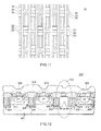
- Fig. 12 is a cross-sectional view of a conventional trench gate power MOSFET 900.
- the conventional trench gate power MOSFET 900 includes an n-type semiconductor base body 902, gates 906 disposed in trenches 904 formed in a surface of the n-type semiconductor base body 902, and MOSFET cells 908 respectively formed between the trenches 904.
- the MOSFET cell 908 includes a p-type body region 910 formed on the surface of the n-type semiconductor base body 902 in a state that the body region 910 is in contact with side surfaces of the trench 904, an n-type source region 912 formed on the surface of the p-type body region 910 in a state that the n-type source region 912 is in contact with the side surfaces of the trench 904, and a p-type contact region 914 formed on the surface of the p-type body region 910 in a state that the p-type contact region 914 is in contact with the n-type source region 912.
- a conductive layer 916 is formed over the MOSFET cells 908, and a source electrode 918 is formed over the conductive layer 916.
- a drain electrode 920 (not shown in the drawing) is formed on a back surface of the n-type semiconductor base body 902.
- a region 922 where the MOSFET cell is not formed exists, and a metal layer 924 which is electrically connected with the source electrode 918 is formed on the surface of the semiconductor base body 902 in such a region 922.
- the metal layer 924 and the conductive layer 916 are formed using the same steps and the same material.
- a Schottky diode which possesses a parallel relationship with the MOSFET is formed (see patent document 1, for example).
- the trench gate power MOSFET 900 when the source electrode 918 is positively biased, an electric current flows into the drain electrode 920 from the source electrode 918 via the metal layer 924 and the n-type semiconductor base body 902 and hence, the trench gate power MOSFET 900 exhibits an advantageous effect that a forward drop voltage VF of an incorporated diode can be suppressed to a low level when the MOSFET is used in the bridge structure.
- the trench gate power MOSFET 900 such a Schottky barrier diode can be integrated into the trench gate power MOSFET in a monolithic manner and hence, the trench gate power MOSFET 900 also acquires an advantageous effect that a product can be miniaturized compared to a case where a Schottky barrier diode is externally mounted on a power MOSFET.
- Patent document 1 US Patent Specification No. 6351018 ( Fig. 1 and Fig. 2 )
- the conventional trench gate power MOSFET 900 has a drawback that a diode leakage current attributed to the Schottky barrier diode is increased along with the elevation of temperature.
- the present invention has been made to overcome the above-mentioned drawbacks, and it is an object of the present invention to provide a trench gate power MOSFET capable of suppressing the increase of a diode leakage current attributed to the elevation of temperature.
- a trench gate power MOSFET includes: a first conductive-type semiconductor base body; gates disposed in trenches formed in a surface of the first conductive-type semiconductor base body; and MOSFET cells including second conductive-type body regions formed on the surface of the first conductive-type semiconductor base body in a state that the second conductive-type body regions are in contact with side surfaces of the trenches, first conductive-type source regions formed on surfaces of the second conductive-type body regions in a state that the first conductive-type source regions are in contact with the side surfaces of the trenches, and second conductive-type contact regions formed on the surfaces of the second conductive-type body regions in a state that the second conductive-type contact regions are in contact with the first conductive-type source regions, wherein the trench gate power MOSFET further includes second conductive-type isolation regions which are formed on the surface of the first conductive-type semiconductor base body and are disposed such that each second conductive-type isolation region is disposed between the MOSFET cells adjacent to each other in the extending direction of
- the pn-junction diode is integrated to the trenchgatepowerMOSFET inplace of a Schottky barrier diode and hence, it is possible to suppress the increase of a diode leakage current attributed to the elevation of temperature.
- the second conductive-type isolation regions are formed in addition to the second conductive-type body regions, and the pn-junction diode is formed between the second conductive-type isolation region and the first conductive-type semiconductor base body and hence, a depth and the impurity concentration of the second conductive-type isolation region can be determined independently from the second conductive-type body region thus ensuring a required withstand voltage.
- the second conductive-type isolation region is disposed between the MOSFET cells adjacent to each other in the extending direction of the trenches, and the pn-junction diode is formed between the second conductive-type isolation region and the first conductive-type semiconductor base body and hence, by forming a portion of a MOSFET-cell-forming region defined between the trenches into the second conductive-type isolation region, an area on which the pn-junction diode is formed can be reduced thus preventing an ON resistance from being increased more than necessity.
- the second conductive-type isolation region is disposed between the MOSFET cells adjacent to each other in the extending direction of the trenches and hence, positioning of a mask in a step for forming the second conductive-type isolation regions does not require considerably high positioning accuracy thus preventing the MOSFET cell from becoming large-sized or a process from becoming complicated attributed to the formation of the second conductive-type isolation regions.
- the impurity concentration in the surface of the second conductive-type isolation region may preferably be set lower than the impurity concentration in the surface of the second conductive-type body region.
- a depth of the second conductive-type isolation region may preferably be smaller than a depth of the second conductive-type body region.
- a total quantity of impurity integrated in the depth direction in the second conductive-type isolation region may preferably be set smaller than a total quantity of impurity integrated in the depth direction in the second conductive-type body region.
- the trench gate power MOSFET of the present invention can form the pn-junction diode with a low forward drop voltage.
- the impurity concentration in the surface of the second conductive-type isolation region may preferably be set to a value equal to or more than 5 ⁇ 10 16 atoms/cm 3 .
- the depth of the second conductive-type isolation region may preferably be set to a value equal to or more than 0.28 ⁇ m.
- the trench gate power MOSFET of the present invention can form the pn-junction diode with a small leakage current.
- a source electrode which is formed so as to cover the first conductive-type source regions, the second conductive-type body regions and the second conductive-type isolation regions may preferably be made of a metal material containing tervalent metal in a state that the first conductive-type is set to an n type.
- a favorable electrical connection can be established between the first conductive-type source region and the source electrode, between the second conductive-type body region and the source electrode, and between the second conductive-type isolation region and the source electrode.
- the second conductive-type body region maypreferablybe disposed between the first conductive-type source region and the second conductive-type isolation region.
- the second conductive-type body region always exists around the first conductive-type source region and hence, there is no possibility that the transistor characteristics are deteriorated attributed to the formation of the second conductive-type isolation region.
- the first conductive-type semiconductor base body may preferably be a first conductive-type epitaxial layer formed on a surface of a semiconductor substrate.
- Fig. 1 is a view for explaining a trench gate power MOSFET 1 according to an embodiment 1.
- Fig. 1(a) is a plan view of the trench gate power MOSFET 1
- Fig. 1(b) is a cross-sectional view taken along a line A 1 -A 1 in Fig. 1(a)
- Fig. 1(c) is a cross-sectional view taken along a line A 2 -A 2 in Fig. 1(a)
- Fig. 1 (d) is a cross-sectional view taken along a line A 3 -A 3 in Fig. 1 (a)
- Fig. 1 (e) is a cross-sectional view taken along a line A 4 -A 4 in Fig. 1 (a) .
- Fig. 2 is a perspective view of the trench gate power MOSFET 1 according to the embodiment 1.
- the trench gate power MOSFET 1 includes, as shown in Fig. 1 and Fig. 2 , an n-type epitaxial layer 12 (first conductive-type semiconductor base body) formed on an n-type silicon substrate 10, gates 18 disposed in trenches 14 formed in a surface of the n-type epitaxial layer 12, and a MOSFET cell including p-type body regions 20 (second conductive-type body regions) formed on the surface of the n-type epitaxial layer 12 in a state that the p-type body region 20 is in contact with side surfaces of the trenches 14, n-type source regions 22 (first conductive-type source regions) formed on the surfaces of the p-type body regions 20 in a state that the n-type source regions 22 are in contact with the side surfaces of the trenches 14, and p-type contact regions 24 (second conductive-type contact regions) formed on the surfaces of the p-type body regions 20 in a state that the p-type contact regions 24 are in contact with the n-type
- the trench gate power MOSFET 1 according to the embodiment 1 further includes p-type isolation regions 26 (second conductive-type isolation regions) each of which is formed on the surface of the n-type epitaxial layer 12 and is disposed between the MOSFET cells adjacent to each other in the extending direction of the trenches 14 out of the MOSFET cells, and a pn-junction diode is formed between the p-type isolation region 26 and the n-type epitaxial layer 12.
- p-type isolation regions 26 second conductive-type isolation regions
- the p-type body region 20 is disposed between the n-type source region 22 and the p-type isolation region 26.
- a source electrode 30 is formed so as to cover the n-type source regions 22, the p-type contact regions 24 and thep-type isolation regions 26 (see Fig. 7(h) ).
- the source electrode 30 is made of aluminum.
- the pn-junction diode is integrated to the trench gate power MOSFET in place of a Schottky barrier diode and hence, it is possible to suppress the increase of a diode leakage current attributed to the elevation of temperature.
- the p-type isolation regions 26 are formed in addition to the p-type body regions 20, and the pn-junction diode is formed between the p-type isolation region 26 and the n-type epitaxial layer 12 and hence, a depth and impurity concentration of the p-type isolation region 2 6 can be determined independently from the p-type body region 20 thus ensuring a required withstand voltage.
- the p-type isolation region 26 is disposed between the MOSFET cells adjacent to each other in the extending direction of the trenches 14, and the pn-junction diode is formed between the p-type isolation region 26 and the n-type epitaxial layer 12 and hence, by forming a portion of a MOSFET-cell-forming region defined between the trenches 14 into the second conductive-type isolation region 26, an area on which the pn-junction diode is formed can be reduced thus preventing an ON resistance from being increased more than necessity.
- the p-type isolation region 26 is disposed between the MOSFET cells adjacent to each other in the extending direction of the trenches 14 and hence, positioning of a mask in a step for forming the p-type isolation regions 26 does not require considerably high positioning accuracy thus preventing the MOSFET cell from becoming large sized or a process from becoming complicated attributed to the formation of the p-type isolation regions 26.
- Fig. 3 is a view showing an impurity concentration profile in the depth direction in the trench gate power MOSFET 1.
- Fig. 3(a) is a view showing the impurity concentration profile in cross section taken along a line B 1 -B 1 in Fig. 1(b)
- Fig. 3(b) is a view showing the impurity concentration profile in cross section taken along a line B 2 -B 2 in Fig. 1(b) .
- the impurity concentration (see Fig. 3 (b) for example, 5x10 16 atoms/cm 3 ) in the surface of the p-type isolation region 26 is lower than the impurity concentration (see Fig. 3(a) , for example, 3 ⁇ 10 17 atoms/cm 3 ) in the surface of the p-type body region 20.
- a depth (for example, 0.3 ⁇ m) of the p-type isolation region 26 is smaller than a depth (for example, 1.0 ⁇ m) of the p-type body region 20.
- a total quantity of impurity integrated in the depth direction in the p-type isolation region 26 is smaller than a total quantity of impurity integrated in the depth direction in the p-type body region 20.
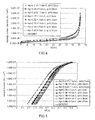
- Fig. 4 is a view showing leakage current density when conditions for forming the p-type isolation region 26 are changed.
- a drain voltage VD is taken on an axis of abscissas
- the leakage current density J is taken on an axis of ordinates.
- Symbol Np indicates surface impurity concentration of the p-type isolation region 26, and symbol xj indicates a depth of the p-type isolation region 26.
- the leakage current density J of the trench gate power MOSFET 1 of the embodiment 1 is not increased except for a case in which the impurity concentration of the p-type isolation region is extremely low (2.1 ⁇ 10 16 atoms/cm 3 ) and the depth of the isolation region is extremely small (0.23 ⁇ m).
- Fig. 5 is a view showing a forward drop voltage VF when conditions for forming the p-type isolation region 26 are changed.
- the forward drop voltage VF is taken on an axis of abscissas, and the current density J corresponding to the forward drop voltage VF is taken on an axis of ordinates.
- Symbol Np indicates surface impurity concentration of the p-type isolation region 26, and symbol xj indicates a depth of the p-type isolation region 26.
- the forward drop voltage VF of the trench gate power MOSFET 1 of the embodiment 1 is lowered corresponding to the decrease of the impurity concentration of the p-type isolation region and the decrease of the depth of the p-type isolation region.
- the impurity concentration in the surface of the p-type isolation region 26 lower than the impurity concentration in the surface of the p-type body region 20 and, at the same time, to set the impurity concentration in the surface of the p-type isolation region 26 to a value equal to or more than 5x10 16 atoms/cm 3 .
- it is preferable to set the total quantity of the impurity integrated in the depth direction in the p-type isolation region 26 smaller than the total quantity of the impurity integrated in the depth direction in the p-type body region 20.
- the impurity concentration, the depth and the total quantity of the impurity in the p-type isolation region 26 are set to values which fall within the above-mentioned ranges, it is possible to form a pn-junction diode which exhibits a small leakage current and a low forward drop voltage.
- the source electrode which is formed so as to cover the n-type source regions 22, the p-type contact regions 24 and the p-type isolation regions 26 is made of aluminum as described above and hence, a favorable electrical connection is established between these regions 22, 24, 26 and the source electrode 30.
- the p-type body region 20 is disposed between the n-type source region 22 and the p-type isolation region 26 and hence, the p-type body region 20 always exists around the n-type source region 22 whereby there is no possibility that the transistor characteristics are deteriorated attributed to the formation of the p-type isolation region 26.
- the n-type epitaxial layer 12 formed on the surface of the silicon substrate 10 is used as the first conductive-type semiconductor base body and hence, by optimizing impurity concentration and a layer thickness of the n-type epitaxial layer 10, it is possible to acquire a trench gate power MOSFET possessing desired ON resistance characteristic and withstand voltage characteristic.
- FIG. 6 and Fig. 7 are views showing respective manufacturing steps of the manufacturing method of the trench gate power MOSFET according to the embodiment 1.
- steps (a) to (h) essential parts in cross section taken along lines A 2 -A 2 , A 3 -A 3 and A 1 -A 1 in Fig. 1 (a) are shown.
- the manufacturing method of the trench gate power MOSFET 1 according to the embodiment 1 includes, as shown in Fig. 6 and Fig. 7 , following steps ranging from (a) a first step to (h) an eighth step in this order.
- the n-type silicon substrate 10 which forms the n-type epitaxial layer 12 on an upper surface thereof is prepared (see Fig. 6 (a) ).
- the impurity concentration of the n-type epitaxial layer 12 is set to 3 ⁇ 10 +15 atoms/cm 3 , for example.
- a silicon oxide film is selectively formed on a surface of the n-type epitaxial layer 12, and the trenches 14 are formed in the surface of the n-type epitaxial layer 12 using the silicon oxide film as a mask.
- the gate insulation film 16 is formed by thermal oxidation.
- the inside of the trench is filled with poly-silicon doped with phosphorous, an upper surface of poly-silicon is etched back and is subject to further thermal oxidation thus forming the gates 18 (see Fig. 6(b) ).
- a surface of the epitaxial layer 12 is leveled.
- boron ions for example, 1.5 ⁇ 10 +13 atoms/cm 2
- thermal annealing is applied (for example, at a temperature of 1100°C for 45 minutes) thus forming the p-type body regions 20 (see Fig. 6(c) ).
- boron ions for example, 2x10 +15 atoms/cm 2
- thermal annealing is applied (for example, at a temperature of 900°C for 30 minutes) thus forming the p-type contact regions 24 (see Fig. 6(d) ).
- boron ions for example, 1.7x10 +12 atoms/cm 2
- symbol M 1 indicates a mask.
- arsenic ions for example, 4x10 +15 atoms/cm 2
- a width of the portion 23 corresponding to the n-type source region 22 is set to 1 ⁇ m or less, for example.
- a distance between the portion 23 corresponding to the n-type source region 22 and the portion 23 corresponding to the n-type source region 22 is set to 7 ⁇ m or less, for example.
- symbol M 2 indicates a mask.
- thermal annealing is applied (for example at a temperature of 1000°C for 10 minutes) thus simultaneously forming the p-type isolation regions 26 and the n-type source regions 22 (see Fig. 7(g) ).
- interlayer insulation films 28 are formed over the trenches, and the source electrode 30 is formed over the interlayer insulation films 28. Further, a drain electrode 32 is formed on a back surface of the silicon substrate 10 (see Fig. 7(h) ).
- the trench gate power MOSFET 1 of the embodiment 1 can be manufactured using the relatively easy method.
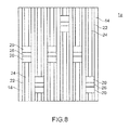
- Fig. 8 is a plan view of a trench gate power MOSFET 1a according to a modification 1.
- the trench gate power MOSFET 1a according to the modification 1 adopts the structure similar to the structure of the trench gate power MOSFET 1 according to the embodiment 1.
- the trench gate power MOSFET 1a according to the modification 1 differs from the trench gate power MOSFET 1 according to the embodiment 1 with respect to a pattern for arranging the p-type isolation regions 26. That is, in the trench gate power MOSFET 1a according to the modification 1, the p-type isolation regions 26 are formed in a more dispersed manner than the p-type isolation regions 26 in the trench gate power MOSFET 1 according to the embodiment 1.
- the trench gate power MOSFET 1a according to the modification 1 differs from the trench gate power MOSFET 1 according to the embodiment 1 with respect to the pattern for arranging the p-type isolation regions 26.
- the pn-junction diode is integrated to the trench gate power MOSFET in place of a Schottky barrier diode and hence, it is possible to suppress the increase of a diode leakage current attributed to the elevation of temperature.
- the p-type isolation regions 26 are formed in addition to the p-type body regions 20, and the pn-junction diode is formed between the p-type isolation region 26 and the n-type epitaxial layer 12 and hence, a depth and impurity concentration of the p-type isolation region 26 can be determined independently from the p-type body region 20 thus ensuring a required withstand voltage.
- the p-type isolation region 26 is disposed between the MOSFET cells adjacent to each other in the extending direction of the trenches 14, and the pn-junction diode is formed between the p-type isolation region 26 and the n-type epitaxial layer 12 and hence, by forming a portion of a MOSFET-cell-forming region defined between the trenches 14 into the p-type isolation region 26, an area on which the pn-junction diode is formed can be reduced thus preventing an ON resistance from being increased more than necessity.
- the p-type isolation region 26 is disposed between the MOSFET cells adjacent to each other in the extending direction of the trenches 14 and hence, positioning of a mask in a step for forming the p-type isolation regions 26 does not require considerably high positioning accuracy thus preventing the MOSFET cell from becoming large sized or a process from becoming complicated attributed to the formation of the p-type isolation regions 26.
- Fig. 9 is a view for explaining a trench gate power MOSFET 2 according to an embodiment 2.
- Fig. 9(a) is a plan view of the trench gate power MOSFET 2
- Fig. 9 (b) is a cross-sectional view taken along a line C-C in Fig. 9 (a) .
- Fig. 10 is a perspective view of the trench gate power MOSFET 2 according to the embodiment 2.
- the trench gate power MOSFET 2 according to the embodiment 2 adopts the structure similar to the structure of the trench gate power MOSFET 1 according to the embodiment 1. However, as shown in Fig. 9 and Fig. 10 , the trench gate power MOSFET 2 according to the embodiment 2 differs from the trench gate power MOSFET 1 according to the embodiment 1 with respect to a pattern for forming the trenches 14. That is, in the trench gate power MOSFET 2 according to the embodiment 2, the trenches 14 are formed in a grid arrangement.
- the trench gate power MOSFET 2 according to the embodiment 2 differs from the trench gate power MOSFET 1 according to the embodiment 1 with respect to the pattern for forming the trenches 14.
- the pn-junction diode is integrated to the trench gate power MOSFET in place of a Schottky barrier diode and hence, it is possible to suppress the increase of a diode leakage current attributed to the elevation of temperature.
- the p-type isolation regions 26 are formed in addition to the p-type body regions 20, and the pn-junction diode is formed between the p-type isolation region 26 and the n-type epitaxial layer 12 and hence, a depth and impurity concentration of the p-type isolation region 26 can be determined independently from the p-type body region 20 thus ensuring a required withstand voltage.
- the p-type isolation region 26 is disposed between the MOSFET cells adjacent to each other in the extending direction of the trenches 14, and the pn-junction diode is formed between the p-type isolation region 26 and the n-type epitaxial layer 12 and hence, by forming a portion of a MOSFET-cell-forming region defined between the trenches 14 into the p-type isolation region 26, an area on which the pn-junction diode is formed can be reduced thus preventing an ON resistance from being increased more than necessity.
- the p-type isolation region 26 is disposed between the MOSFET cells adjacent to each other in the extending direction of the trenches 14 and hence, positioning of a mask in a step for forming the p-type isolation regions 26 does not require considerably high positioning accuracy thus preventing the MOSFET cell from becoming large sized or a process from becoming complicated attributed to the formation of the p-type isolation regions 26.
- Fig. 11 is a plan view of a trench gate power MOSFET 2a according to a modification 2.
- the trench gate power MOSFET 2a according to the modification 2 adopts the structure similar to the structure of the trench gate power MOSFET 2 according to the embodiment 2.
- the trench gate power MOSFET 2a according to the modification 2 differs from the trench gate power MOSFET 2 according to the embodiment 2 with respect to a pattern for forming the MOSFET cells. That is, in the trench gate power MOSFET 2a according to the modification 2, the MOSFET cells are formed in a staggered arrangement.
- the trench gate power MOSFET 2a according to the modification 2 differs from the trench gate power MOSFET 2 according to the embodiment 2 with respect to the pattern for forming the MOSFET cells.
- the pn-junction diode is integrated to the trench gate power MOSFET in place of a Schottky barrier diode and hence, it is possible to suppress the increase of a diode leakage current attributed to the elevation of temperature.
- the p-type isolation regions 26 are formed in addition to the p-type body regions 20, and the pn-junction diode is formed between the p-type isolation region 26 and the n-type epitaxial layer 12 and hence, a depth and impurity concentration of the p-type isolation region 26 can be determined independently from the p-type body region 20 thus ensuring a required withstand voltage.
- the p-type isolation region 26 is disposed between the MOSFET cells adjacent to each other in the extending direction of the trenches 14, and the pn-junction diode is formed between the p-type isolation region 26 and the n-type epitaxial layer 12 and hence, by forming a portion of a MOSFET-cell-forming region defined between the trenches 14 into the p-type isolation region 26, an area on which the pn-junction diode is formed can be reduced thus preventing an ON resistance from being increased more than necessity.
- the p-type isolation region 26 is disposed between the MOSFET cells adjacent to each other in the extending direction of the trenches 14 and hence, positioning of a mask in a step for forming the p-type isolation regions 26 does not require considerably high positioning accuracy thus preventing the MOSFET cell from becoming large sized or a process from becoming complicated attributed to the formation of the p-type isolation regions 26.
- the present invention is not limited to the above-mentioned respective embodiments, and various modifications can be made without departing from the gist of the present invention. For example, the following modification can be made.
- 1, 1a, 2, 2a, 900 trench gate power MOSFET, 10: siliconsubstrate, 12: n-type epitaxial layer, 14: trench, 16: gate insulation film, 18: gate, 20: p-type body region, 22: n-type source region, 24: p-type contact region, 26: p-type isolation region, 28: interlayer insulation film, 30: source electrode, 32: drain electrode, M 1 , M 2 : mask
Landscapes
- Metal-Oxide And Bipolar Metal-Oxide Semiconductor Integrated Circuits (AREA)
- Electrodes Of Semiconductors (AREA)
- Insulated Gate Type Field-Effect Transistor (AREA)
Applications Claiming Priority (1)
| Application Number | Priority Date | Filing Date | Title |
|---|---|---|---|
| PCT/JP2005/017417 WO2007034547A1 (ja) | 2005-09-21 | 2005-09-21 | トレンチゲートパワーmosfet及びその製造方法 |
Publications (3)
| Publication Number | Publication Date |
|---|---|
| EP1947699A1 true EP1947699A1 (de) | 2008-07-23 |
| EP1947699A8 EP1947699A8 (de) | 2008-10-01 |
| EP1947699A4 EP1947699A4 (de) | 2009-04-08 |
Family
ID=37888608
Family Applications (1)
| Application Number | Title | Priority Date | Filing Date |
|---|---|---|---|
| EP05785935A Withdrawn EP1947699A4 (de) | 2005-09-21 | 2005-09-21 | Graben-gate-leistungs-mosfet |
Country Status (4)
| Country | Link |
|---|---|
| US (1) | US20090250750A1 (de) |
| EP (1) | EP1947699A4 (de) |
| JP (1) | JPWO2007034547A1 (de) |
| WO (1) | WO2007034547A1 (de) |
Families Citing this family (6)
| Publication number | Priority date | Publication date | Assignee | Title |
|---|---|---|---|---|
| KR101396611B1 (ko) * | 2010-04-28 | 2014-05-16 | 닛산 지도우샤 가부시키가이샤 | 반도체 장치 |
| KR101148694B1 (ko) | 2010-12-09 | 2012-05-25 | 삼성전기주식회사 | 질화물계 반도체 소자 및 그 제조 방법 |
| WO2016052203A1 (ja) | 2014-09-30 | 2016-04-07 | 三菱電機株式会社 | 半導体装置 |
| KR102219504B1 (ko) * | 2015-03-18 | 2021-02-25 | 한국전자통신연구원 | 전계 효과 전력 전자 소자 및 그의 제조 방법 |
| US12495577B2 (en) | 2022-08-17 | 2025-12-09 | Analog Devices, Inc. | Self-aligned silicide gate for discrete shielded-gate trench power MOSFET |
| EP4421877A1 (de) * | 2023-02-24 | 2024-08-28 | Infineon Technologies Austria AG | Halbleiterchip und verfahren zur herstellung davon |
Family Cites Families (8)
| Publication number | Priority date | Publication date | Assignee | Title |
|---|---|---|---|---|
| JPH03238871A (ja) * | 1990-02-15 | 1991-10-24 | Mitsubishi Electric Corp | 半導体装置およびその製造方法 |
| US5856692A (en) * | 1995-06-02 | 1999-01-05 | Siliconix Incorporated | Voltage-clamped power accumulation-mode MOSFET |
| US6351018B1 (en) * | 1999-02-26 | 2002-02-26 | Fairchild Semiconductor Corporation | Monolithically integrated trench MOSFET and Schottky diode |
| GB9906247D0 (en) * | 1999-03-18 | 1999-05-12 | Koninkl Philips Electronics Nv | An electronic device comprising a trench gate field effect device |
| US7126169B2 (en) * | 2000-10-23 | 2006-10-24 | Matsushita Electric Industrial Co., Ltd. | Semiconductor element |
| JP3502371B2 (ja) * | 2000-10-23 | 2004-03-02 | 松下電器産業株式会社 | 半導体素子 |
| JP2004119513A (ja) * | 2002-09-24 | 2004-04-15 | Toshiba Corp | 半導体装置及びその製造方法 |
| JP4799829B2 (ja) * | 2003-08-27 | 2011-10-26 | 三菱電機株式会社 | 絶縁ゲート型トランジスタ及びインバータ回路 |
-
2005
- 2005-09-21 US US12/066,984 patent/US20090250750A1/en not_active Abandoned
- 2005-09-21 JP JP2007536368A patent/JPWO2007034547A1/ja not_active Withdrawn
- 2005-09-21 WO PCT/JP2005/017417 patent/WO2007034547A1/ja not_active Ceased
- 2005-09-21 EP EP05785935A patent/EP1947699A4/de not_active Withdrawn
Also Published As
| Publication number | Publication date |
|---|---|
| WO2007034547A1 (ja) | 2007-03-29 |
| US20090250750A1 (en) | 2009-10-08 |
| EP1947699A8 (de) | 2008-10-01 |
| EP1947699A4 (de) | 2009-04-08 |
| JPWO2007034547A1 (ja) | 2009-03-19 |
Similar Documents
| Publication | Publication Date | Title |
|---|---|---|
| EP1168455B1 (de) | Leistungshalbleiter-Schaltelement | |
| US7649223B2 (en) | Semiconductor device having superjunction structure and method for manufacturing the same | |
| US6979862B2 (en) | Trench MOSFET superjunction structure and method to manufacture | |
| US8106447B2 (en) | Semiconductor device and method of manufacturing the same | |
| US7858475B2 (en) | Method for manufacturing a vertical transistor that includes a super junction structure | |
| US10263070B2 (en) | Method of manufacturing LV/MV super junction trench power MOSFETs | |
| US6764906B2 (en) | Method for making trench mosfet having implanted drain-drift region | |
| CN110718546B (zh) | 绝缘栅极半导体器件及其制造方法 | |
| US6639278B2 (en) | Semiconductor device | |
| JP4813762B2 (ja) | 半導体装置及びその製造方法 | |
| US8519476B2 (en) | Method of forming a self-aligned charge balanced power DMOS | |
| US9911816B2 (en) | Semiconductive device and associated method of manufacture | |
| CN101908541B (zh) | 半导体装置及其制造方法 | |
| US8169023B2 (en) | Power semiconductor device | |
| US8125022B2 (en) | Semiconductor device and method of manufacturing the same | |
| CN208127215U (zh) | 包括终止结构的电子设备 | |
| JP2019521529A (ja) | パワーデバイス及びその製造方法 | |
| CN100367510C (zh) | 具有边缘结构的半导体器件 | |
| US7608510B2 (en) | Alignment of trench for MOS | |
| US6969657B2 (en) | Superjunction device and method of manufacture therefor | |
| KR101960547B1 (ko) | 반도체 장치 및 그 제조 방법 | |
| CN101471381B (zh) | 沟槽栅mosfet及其制造方法 | |
| EP1947699A1 (de) | Graben-gate-leistungs-mosfet | |
| JP5266829B2 (ja) | 半導体装置及びその製造方法 | |
| US9960269B2 (en) | Semiconductor device and method of manufacturing the same |
Legal Events
| Date | Code | Title | Description |
|---|---|---|---|
| PUAI | Public reference made under article 153(3) epc to a published international application that has entered the european phase |
Free format text: ORIGINAL CODE: 0009012 |
|
| 17P | Request for examination filed |
Effective date: 20080318 |
|
| AK | Designated contracting states |
Kind code of ref document: A1 Designated state(s): DE FR GB IT |
|
| RAP1 | Party data changed (applicant data changed or rights of an application transferred) |
Owner name: SHINDENGEN ELECTRIC MANUFACTURING CO., LTD. |
|
| RIN1 | Information on inventor provided before grant (corrected) |
Inventor name: TAKEMORI, TOSHIYUKIC/O SHINDENGEN ELECTRIC MANUFAC Inventor name: MATSUYAMA, KAZUSHIGEC/O SHINDENGEN ELECTRIC MANUFA Inventor name: WATANABE, YUJIC/O SHINDENGEN ELECTRIC MANUFACTURIN Inventor name: SASAOKA, FUMINORIC/O SHINDENGEN ELECTRIC MANUFACTU Inventor name: ITOI, MASATOC/O SHINDENGEN ELECTRIC MANUFACTURING Inventor name: OSHIMA, KUNIHIKOC/O SHINDENGEN ELECTRIC MANUFACTUR |
|
| DAX | Request for extension of the european patent (deleted) | ||
| RBV | Designated contracting states (corrected) |
Designated state(s): DE FR GB IT |
|
| A4 | Supplementary search report drawn up and despatched |
Effective date: 20090309 |
|
| RIC1 | Information provided on ipc code assigned before grant |
Ipc: H01L 29/78 20060101AFI20070604BHEP Ipc: H01L 21/336 20060101ALI20090303BHEP Ipc: H01L 29/06 20060101ALN20090303BHEP Ipc: H01L 29/10 20060101ALI20090303BHEP Ipc: H01L 29/423 20060101ALN20090303BHEP |
|
| STAA | Information on the status of an ep patent application or granted ep patent |
Free format text: STATUS: THE APPLICATION IS DEEMED TO BE WITHDRAWN |
|
| 18D | Application deemed to be withdrawn |
Effective date: 20090606 |