EP1947688A1 - Film peeling method and film peeling apparatus - Google Patents
Film peeling method and film peeling apparatus Download PDFInfo
- Publication number
- EP1947688A1 EP1947688A1 EP06780977A EP06780977A EP1947688A1 EP 1947688 A1 EP1947688 A1 EP 1947688A1 EP 06780977 A EP06780977 A EP 06780977A EP 06780977 A EP06780977 A EP 06780977A EP 1947688 A1 EP1947688 A1 EP 1947688A1
- Authority
- EP
- European Patent Office
- Prior art keywords
- wafer
- film
- peeling
- groove
- tape
- Prior art date
- Legal status (The legal status is an assumption and is not a legal conclusion. Google has not performed a legal analysis and makes no representation as to the accuracy of the status listed.)
- Withdrawn
Links
Images




Classifications
-
- H—ELECTRICITY
- H10—SEMICONDUCTOR DEVICES; ELECTRIC SOLID-STATE DEVICES NOT OTHERWISE PROVIDED FOR
- H10P—GENERIC PROCESSES OR APPARATUS FOR THE MANUFACTURE OR TREATMENT OF DEVICES COVERED BY CLASS H10
- H10P72/00—Handling or holding of wafers, substrates or devices during manufacture or treatment thereof
- H10P72/70—Handling or holding of wafers, substrates or devices during manufacture or treatment thereof for supporting or gripping
-
- H—ELECTRICITY
- H10—SEMICONDUCTOR DEVICES; ELECTRIC SOLID-STATE DEVICES NOT OTHERWISE PROVIDED FOR
- H10P—GENERIC PROCESSES OR APPARATUS FOR THE MANUFACTURE OR TREATMENT OF DEVICES COVERED BY CLASS H10
- H10P72/00—Handling or holding of wafers, substrates or devices during manufacture or treatment thereof
- H10P72/04—Apparatus for manufacture or treatment
- H10P72/0442—Apparatus for placing on an insulating substrate, e.g. tape
-
- B—PERFORMING OPERATIONS; TRANSPORTING
- B23—MACHINE TOOLS; METAL-WORKING NOT OTHERWISE PROVIDED FOR
- B23K—SOLDERING OR UNSOLDERING; WELDING; CLADDING OR PLATING BY SOLDERING OR WELDING; CUTTING BY APPLYING HEAT LOCALLY, e.g. FLAME CUTTING; WORKING BY LASER BEAM
- B23K26/00—Working by laser beam, e.g. welding, cutting or boring
- B23K26/36—Removing material
- B23K26/40—Removing material taking account of the properties of the material involved
-
- H—ELECTRICITY
- H10—SEMICONDUCTOR DEVICES; ELECTRIC SOLID-STATE DEVICES NOT OTHERWISE PROVIDED FOR
- H10P—GENERIC PROCESSES OR APPARATUS FOR THE MANUFACTURE OR TREATMENT OF DEVICES COVERED BY CLASS H10
- H10P52/00—Grinding, lapping or polishing of wafers, substrates or parts of devices
-
- H—ELECTRICITY
- H10—SEMICONDUCTOR DEVICES; ELECTRIC SOLID-STATE DEVICES NOT OTHERWISE PROVIDED FOR
- H10P—GENERIC PROCESSES OR APPARATUS FOR THE MANUFACTURE OR TREATMENT OF DEVICES COVERED BY CLASS H10
- H10P72/00—Handling or holding of wafers, substrates or devices during manufacture or treatment thereof
- H10P72/70—Handling or holding of wafers, substrates or devices during manufacture or treatment thereof for supporting or gripping
- H10P72/76—Handling or holding of wafers, substrates or devices during manufacture or treatment thereof for supporting or gripping using mechanical means, e.g. clamps or pinches
- H10P72/7604—Handling or holding of wafers, substrates or devices during manufacture or treatment thereof for supporting or gripping using mechanical means, e.g. clamps or pinches the wafers being placed on a susceptor, stage or support
- H10P72/7618—Handling or holding of wafers, substrates or devices during manufacture or treatment thereof for supporting or gripping using mechanical means, e.g. clamps or pinches the wafers being placed on a susceptor, stage or support characterised by a movable susceptor, stage or support, others than those only rotating on their own vertical axis, e.g. susceptors on a rotating carrousel
-
- B—PERFORMING OPERATIONS; TRANSPORTING
- B23—MACHINE TOOLS; METAL-WORKING NOT OTHERWISE PROVIDED FOR
- B23K—SOLDERING OR UNSOLDERING; WELDING; CLADDING OR PLATING BY SOLDERING OR WELDING; CUTTING BY APPLYING HEAT LOCALLY, e.g. FLAME CUTTING; WORKING BY LASER BEAM
- B23K2103/00—Materials to be soldered, welded or cut
- B23K2103/50—Inorganic materials other than metals or composite materials
-
- Y—GENERAL TAGGING OF NEW TECHNOLOGICAL DEVELOPMENTS; GENERAL TAGGING OF CROSS-SECTIONAL TECHNOLOGIES SPANNING OVER SEVERAL SECTIONS OF THE IPC; TECHNICAL SUBJECTS COVERED BY FORMER USPC CROSS-REFERENCE ART COLLECTIONS [XRACs] AND DIGESTS
- Y10—TECHNICAL SUBJECTS COVERED BY FORMER USPC
- Y10T—TECHNICAL SUBJECTS COVERED BY FORMER US CLASSIFICATION
- Y10T156/00—Adhesive bonding and miscellaneous chemical manufacture
- Y10T156/10—Methods of surface bonding and/or assembly therefor
- Y10T156/1089—Methods of surface bonding and/or assembly therefor of discrete laminae to single face of additional lamina
- Y10T156/1092—All laminae planar and face to face
-
- Y—GENERAL TAGGING OF NEW TECHNOLOGICAL DEVELOPMENTS; GENERAL TAGGING OF CROSS-SECTIONAL TECHNOLOGIES SPANNING OVER SEVERAL SECTIONS OF THE IPC; TECHNICAL SUBJECTS COVERED BY FORMER USPC CROSS-REFERENCE ART COLLECTIONS [XRACs] AND DIGESTS
- Y10—TECHNICAL SUBJECTS COVERED BY FORMER USPC
- Y10T—TECHNICAL SUBJECTS COVERED BY FORMER US CLASSIFICATION
- Y10T156/00—Adhesive bonding and miscellaneous chemical manufacture
- Y10T156/11—Methods of delaminating, per se; i.e., separating at bonding face
- Y10T156/1168—Gripping and pulling work apart during delaminating
-
- Y—GENERAL TAGGING OF NEW TECHNOLOGICAL DEVELOPMENTS; GENERAL TAGGING OF CROSS-SECTIONAL TECHNOLOGIES SPANNING OVER SEVERAL SECTIONS OF THE IPC; TECHNICAL SUBJECTS COVERED BY FORMER USPC CROSS-REFERENCE ART COLLECTIONS [XRACs] AND DIGESTS
- Y10—TECHNICAL SUBJECTS COVERED BY FORMER USPC
- Y10T—TECHNICAL SUBJECTS COVERED BY FORMER US CLASSIFICATION
- Y10T156/00—Adhesive bonding and miscellaneous chemical manufacture
- Y10T156/19—Delaminating means
- Y10T156/195—Delaminating roller means
-
- Y—GENERAL TAGGING OF NEW TECHNOLOGICAL DEVELOPMENTS; GENERAL TAGGING OF CROSS-SECTIONAL TECHNOLOGIES SPANNING OVER SEVERAL SECTIONS OF THE IPC; TECHNICAL SUBJECTS COVERED BY FORMER USPC CROSS-REFERENCE ART COLLECTIONS [XRACs] AND DIGESTS
- Y10—TECHNICAL SUBJECTS COVERED BY FORMER USPC
- Y10T—TECHNICAL SUBJECTS COVERED BY FORMER US CLASSIFICATION
- Y10T29/00—Metal working
- Y10T29/49—Method of mechanical manufacture
- Y10T29/49815—Disassembling
-
- Y—GENERAL TAGGING OF NEW TECHNOLOGICAL DEVELOPMENTS; GENERAL TAGGING OF CROSS-SECTIONAL TECHNOLOGIES SPANNING OVER SEVERAL SECTIONS OF THE IPC; TECHNICAL SUBJECTS COVERED BY FORMER USPC CROSS-REFERENCE ART COLLECTIONS [XRACs] AND DIGESTS
- Y10—TECHNICAL SUBJECTS COVERED BY FORMER USPC
- Y10T—TECHNICAL SUBJECTS COVERED BY FORMER US CLASSIFICATION
- Y10T29/00—Metal working
- Y10T29/49—Method of mechanical manufacture
- Y10T29/49815—Disassembling
- Y10T29/49819—Disassembling with conveying of work or disassembled work part
-
- Y—GENERAL TAGGING OF NEW TECHNOLOGICAL DEVELOPMENTS; GENERAL TAGGING OF CROSS-SECTIONAL TECHNOLOGIES SPANNING OVER SEVERAL SECTIONS OF THE IPC; TECHNICAL SUBJECTS COVERED BY FORMER USPC CROSS-REFERENCE ART COLLECTIONS [XRACs] AND DIGESTS
- Y10—TECHNICAL SUBJECTS COVERED BY FORMER USPC
- Y10T—TECHNICAL SUBJECTS COVERED BY FORMER US CLASSIFICATION
- Y10T29/00—Metal working
- Y10T29/49—Method of mechanical manufacture
- Y10T29/49815—Disassembling
- Y10T29/49822—Disassembling by applying force
-
- Y—GENERAL TAGGING OF NEW TECHNOLOGICAL DEVELOPMENTS; GENERAL TAGGING OF CROSS-SECTIONAL TECHNOLOGIES SPANNING OVER SEVERAL SECTIONS OF THE IPC; TECHNICAL SUBJECTS COVERED BY FORMER USPC CROSS-REFERENCE ART COLLECTIONS [XRACs] AND DIGESTS
- Y10—TECHNICAL SUBJECTS COVERED BY FORMER USPC
- Y10T—TECHNICAL SUBJECTS COVERED BY FORMER US CLASSIFICATION
- Y10T29/00—Metal working
- Y10T29/53—Means to assemble or disassemble
- Y10T29/53683—Spreading parts apart or separating them from face to face engagement
Definitions
- the present invention relates to a film peeling method of peeling a film stuck onto a front surface of a wafer and specifically a film peeling method of peeling a front surface protection film stuck onto a front surface of a wafer.
- the present invention also relates to a film peeling device for executing this film peeling method.
- back grinding back surface grinding
- a surface protection film is stuck onto the front surface of the wafer, the front surface of the wafer is sucked onto a suction table, and the back surface of the wafer is ground.
- chamfer portions are formed in a peripheral portion of the wafer to prevent the generation of dust, the width of a cross-section of the wafer at an edge portion is reduced toward to a forward end portion. Since there is a requirement to grind the back surface of the wafer, beyond half of the wafer thickness, the thin chamfered edge becomes too thin.
- Japanese Unexamined Patent Publication No. 2000-173961 discloses the following technique. A cutout portion is formed in a boundary between a chamfer portion of the peripheral portion and a flat portion of the wafer. Then, a back surface of the wafer is ground until the wafer thickness is reduced exceeding the depth of the cutout portion. In this case, if there are cracks or damage in the peripheral portion of the wafer, the occurrence of cracks or damage can be stopped at the cutout portion. Accordingly, deterioration of a semiconductor element arranged in the flat portion of the wafer can be prevented. Concerning this matter, refer to Japanese Unexamined Patent Publication No. 2000-173961 .
- sticking the front surface protection film and grinding the back surface of the wafer are closely related to each other.
- the surface protection film Since the wafer thickness is considerably decreased after grinding the back surface of the wafer, when the front surface protective film is peeled away from the wafer after grinding the back surface, it is necessary to prevent the semiconductor element arranged on the wafer from being damaged.
- the device described in Reference Document 1 makes it possible to prevent the generation of cracks or damage on the wafer at the time of grinding the back surface.
- the front surface protection film away from the wafer after grinding the back surface of the wafer there is a possibility that the peripheral portion of the wafer may become cracked or damaged.
- An object of the present invention is to provide a film peeling method capable of preventing a wafer from being damaged when a front surface protection film, which is stuck onto a front surface of the wafer, is peeled away from the wafer.
- Another object of the present invention is to provide a film peeling device for executing this film peeling method.
- the first aspect provides a film peeling method for peeling a film stuck to a first portion including a peripheral portion of a wafer, and also stuck to a second portion located inward with respect to the first portion, comprising the steps of: moving relatively the first portion and/or the second portion of the wafer so that the film of the first portion can be located at a position higher than the film of the second portion; drawing out a peeling tape onto the film stuck onto the first and the second portion; and pressing a peeling means against the film in the first portion via the peeling tape, wherein when the peeling means is moved along the first portion, the film is peeled away from the first and second portion of the wafer.
- the first portion is located at a position higher than the second portion and the peeling means is only pressed against the first portion via the peeling tape. Accordingly, a load from the peeling means is only applied on the first portion of the wafer, i.e., the load from the peeling means is applied only on a portion containing the peripheral portion of the wafer, which is not used in the future. Therefore, even if the first portion of the wafer is cracked or damaged, the second portion, in which the semiconductor element is formed, is not affected by the crack or damage caused in the first portion. Accordingly, in the first aspect, the film can be peeled away from the wafer without damaging the second portion of the wafer after the grinding of the back surface.
- the second aspect provides a film peeling method comprising the steps of: forming a groove on one face of a wafer along an entire peripheral portion of the wafer inside the peripheral portion of the wafer; sticking a film onto the face of the wafer on which the groove is formed; and grinding a face of the wafer, which is on the opposite side of the wafer, until reaching at least a bottom portion of the groove so that the wafer can be divided into a first portion including the peripheral portion and the second portion located inward with respect to the first portion, the film peeling method further comprising: moving relatively the first portion and/or the second portion of the wafer so that the film of the first portion can be located at a position higher than the film of the second portion; drawing out a peeling tape onto the film stuck onto the first and the second portion; and pressing a peeling means against the film in the first portion via the peeling tape, wherein when the peeling means is moved along the first portion, the film is peeled away from the first and the second portion of the wafer.
- the first portion is located at a position higher than the second portion and the peeling means is pressed only against the first portion via the peeling tape. Accordingly, a load from the peeling means is applied only on the first portion of the wafer, i.e., the load from the peeling means is applied upon only a portion containing the peripheral portion of the wafer, which is not used in the future. Therefore, even if the first portion of the wafer is cracked or damaged, the second portion, in which the semiconductor element is formed, is not affected by the cracks or damage caused in the first portion. Accordingly, in the second aspect, the film can be peeled away from the wafer without damaging the second portion of the wafer after grinding of the back surface.
- cracks or damage which may form in the peripheral portion of the wafer, can be stopped at the groove position. Therefore, the generation of cracks or damage caused at the time of grinding the back surface can be stopped in a portion containing the peripheral portion of the wafer, i.e., the generation of cracks or damage can be stopped only in the first portion.
- the third aspect provides a film peeling method comprising the steps of: sticking a film onto one face of a wafer; grinding a face on the opposite side to the one face of the wafer; and forming a groove on the opposite side of the wafer along an overall peripheral portion of the wafer inside the peripheral portion of the wafer so that the groove can reach the one side of the wafer, wherein the wafer is divided into a first portion, which contains the peripheral portion, and a second portion located inward with respect to the first portion, the film peeling method further comprising the steps of: moving relatively the first portion and/or the second portion of the wafer so that the film of the first portion can be located at a position higher than the film of the second portion; drawing out a peeling tape onto the film stuck onto the first and the second portion; and pressing a peeling means against the first portion film via the peeling tape, wherein the film is peeled away from the first and the second portion when the peeling means is moved along the first portion.
- the fourth aspect provides a film peeling method as in aspect 2 or 3, wherein the groove is formed when a reforming region is formed in the wafer by irradiating laser beams.
- the groove can be formed on the surface of the wafer without generating cracks which are located out of a cutting line and also without melting the front surface of the wafer.
- the fifth aspect provides a film peeling method as in one of aspects 1 to 4, wherein the groove is formed on a boundary between the chamfer portion and the flat portion of the wafer or inside the boundary.
- a step portion is formed between the first and the second portion so that the peeling means can not press the second portion. Accordingly, it is possible to reduce a distance of moving the first portion and/or the second portion.
- the sixth aspect provides a film peeling device for peeling a film stuck onto a first portion containing a peripheral portion of a wafer and also stuck onto a second portion located inward with respect to the first portion, comprising: a moving means for relatively moving the first portion and/or second portion so that the film of the first portion of the wafer can be located at a position higher than the film of the second portion; a tape drawing means for drawing out a peeling tape onto the film stuck onto the first and the second portion; and a peeling means for peeling the film from the first and the second portion of the wafer when the peeling tape drawn out from the tape drawing means is pressed against only the first portion film and moved along the first portion.
- the first portion is located at a position higher than the second portion and the peeling means is pressed against only the first portion via the peeling tape. Accordingly, a load from the peeling means is applied upon only the first portion of the wafer, i.e., the load from the peeling means is applied upon only a portion containing the peripheral portion of the wafer.
- This first portion is not used in the future. Therefore, even if the first portion of the wafer is cracked or damaged, the second portion, in which the semiconductor element is formed, is not affected by the cracks or damage caused in the first portion. Accordingly, in the sixth aspect, the film can be peeled away from the wafer without damaging the second portion of the wafer after the completion of grinding the back surface.
- the seventh aspect provides a film peeling device comprising: a groove forming means for forming a groove inside a peripheral portion of a wafer along the overall peripheral portion of the wafer on one face of the wafer; a film sticking means for sticking a film onto the one face of the wafer on which the groove has been formed; and a grinding means for grinding a face of the wafer opposite to the one face until reaching at least a bottom portion of the groove, wherein the wafer is divided into a first portion containing the peripheral portion and a second portion located inward the first portion, the film peeling device further comprising: a moving means for relatively moving the first portion and/or second portion so that the film of the first portion of the wafer can be located at a position higher than the film of the second portion; a tape drawing means for drawing out a peeling tape onto the film stuck onto the first and the second portion; and a peeling means for peeling the film from the first and the second portion of the wafer when the peeling tape drawn out from the tape drawing means is pressed against only
- the first portion is located at a position higher than the second portion and the peeling means is pressed against only the first portion via the peeling tape. Accordingly, a load from the peeling means is applied only on the first portion of the wafer, i.e., the load from the peeling means is applied upon only a portion containing the peripheral portion of the wafer, which is not used in the future. Therefore, even if the first portion of the wafer is cracked or damaged, the second portion, in which the semiconductor element is formed, is not affected by the cracks or damage caused in the first portion. Accordingly, in the seventh aspect, the film can be peeled away from the wafer without damaging the second portion of the wafer after the completion of grinding the back surface.
- the seventh embodiment at the time of grinding the face of the wafer opposed to the one face, i.e., at the time of grinding the back surface of the wafer, cracks or damage, which proceed from the peripheral portion of the wafer, can be stopped at the groove position. Therefore, the generation of cracks or damage caused at the time of grinding the back surface can be stopped in a portion containing the peripheral portion of the wafer, i.e., the generation of cracks or damage can be stopped only in the first portion.
- the eighth aspect provides a film peeling device comprising: a film sticking means for sticking a film onto one face of a wafer; a grinding means for grinding a face on the opposite side to the one face of the wafer; and a groove forming means for forming a groove on the opposite face of the wafer along an overall peripheral portion of the wafer inside the peripheral portion until the groove reaches the one face of the wafer, wherein the wafer is divided into a first portion containing the peripheral portion and a second portion located inward the first portion, the film peeling device further comprising: a moving means for relatively moving the first portion and/or second portion so that the film of the first portion of the wafer can be located at a position higher than the film of the second portion; a tape drawing means for drawing out a peeling tape onto the film stuck onto the first and the second portion; and a peeling means for peeling the film from the first and the second portion of the wafer when the peeling tape drawn out from the tape drawing means is pressed against only the first portion film and moved along the
- the ninth aspect provides a film peeling device as in the aspect 7 or 8, wherein the groove is formed when a reforming region is formed in the wafer by irradiating laser beams.
- the groove can be formed on the surface of the wafer without generating cracks which are located out of a cutting line and also without melting the front surface of the wafer.
- the tenth aspect provides a film peeling device as in one of aspects 6 to 9, wherein the groove is formed on a boundary between the chamfer portion and the flat portion of the wafer or inside the boundary.
- a step portion is formed between the first and the second portion so that the peeling means can not press the second portion. Accordingly, it is possible to reduce a distance of moving the first portion and/or the second portion.
- each aspect it is possible to provide a common advantage that the wafer can be prevented from being damaged at the time of peeling the film stuck onto the front surface of the wafer.
- the ninth aspect it is possible to provide an advantage that the front surface of the wafer is not melted.
- Fig. 1 is a schematic illustration showing a wafer processing device of the present invention.
- Fig. 2 is a view showing a wafer.
- a plurality of circuit patterns C which are formed into a grid-shape in the previous step, are provided.
- all the circuit patterns C are formed on the flat portion 27 of the wafer 20.
- a peripheral portion of the wafer 20 located in the periphery of the flat portion 27 is formed into a chamfer portion 28.
- no circuit patterns C are formed on the wafer 20 described above is supplied to the wafer processing device 100 shown in Fig. 1 .
- the wafer processing device 100 includes: a preceding dicing unit 150 for forming a groove or a cutout portion on the front surface 21 of the wafer 20; a sticking unit 200 for sticking a front surface protection film 3 onto the front surface 21 of the wafer 20; an inversion unit 300 for inverting the wafer 20 upside down; a back surface grinding unit 350 for grinding a back surface 22 of the wafer 20; a UV irradiation unit 400 for irradiating ultraviolet rays (UV) onto the front surface protection film 3 of the wafer 20; and a peeling unit 500 for peeling the front surface protection film 2 of the wafer 20.
- Conveying devices for example robot arms, for conveying the wafer 20 between the respective units are used. However, since these conveying devices are of the commonly used type, they are not shown in the drawings and the explanations are omitted here.
- the wafer 20 is first supplied to the preceding dicing unit 150 of the wafer processing device 100.
- the front surface 21 of the wafer 20 is diced in the preceding dicing unit 150.
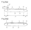
- Fig. 3a is a view showing a state of dicing executed in the preceding dicing unit.
- the wafer 20 is arranged in such a manner that the front surface 21 of the wafer 20 is directed upward.
- the groove 25 is formed on the front surface 21 of the wafer 20 by the relatively small dicing blade 151.
- the groove 25 is formed on a boundary between the chamfer portion 28 and the flat portion 27 of the wafer 20.
- the groove 25 may be formed on the flat portion 27 side with respect to the boundary.
- the annular groove 25 can be formed.
- the depth of the groove 25 shown in Fig. 3a is approximately a half of the thickness of the wafer 20.
- the depth of the groove 25 may be more shallow than that.
- the groove 25 is formed by the dicing blade 151.
- the groove 25 may be formed by other methods. It is also possible to form the groove 25 by a laser beam dicing device.
- Fig. 4 is a sectional side view for explaining laser beam dicing.
- laser beams V are irradiated from a laser beam source not shown onto the front surface 21 side of the wafer 20 through the condenser lens 85.
- the condensing point 84 is adjusted at a position inside the wafer 20 somewhat close to the front surface 21 of the wafer 20. Due to the foregoing, a reforming region is formed around the condensing point 84. Then, when the laser beam V and the condenser lens 85 are moved along the arrow X3, the belt-shaped reforming region 86 is formed inside the wafer 20.
- the reforming region is formed in such a manner that the laser beam V is transmitted through the wafer 20 and the multiple photon absorption is generated in the wafer 20. Accordingly, the laser beam V is seldom absorbed by the wafer 20 on the front surface 21 of the wafer 20. As a result, there is no possibility that the front surface 21 of the wafer is melted. Further, there is no possibility that cracks, which are out of the cutting line, are generated on the front surface of the wafer.
- the groove 25 the width of which corresponds to the width of the laser beam V, is formed.
- Fig. 3b is a view showing a state of sticking the front surface protection film 3 in the sticking unit.
- the front surface protection film 3 is stuck onto the front surface 21 of the wafer 20.
- the front surface protection film 3 has a function of protecting the circuit pattern C, which is formed on the front surface 21 of the wafer, in the back-grinding step executed later.
- the wafer 20 is conveyed from the sticking unit 20 to the inversion unit 300.
- the inversion unit 300 has a function of inverting the wafer 20.
- the wafer 20, onto the front surface 21 of which the front surface protection film 3 is stuck is arranged so that the front surface 21 can be directed upward. Accordingly, in the inversion unit 300, the above wafer 20 is inverted upside down and the front surface 21 of the wafer 20, onto which the surface protection film 3 is stuck, is directed downward.
- the wafer 20 may only pass through the inversion unit 300 without being inverted.
- Fig. 5a is a schematic side view showing a state in which the back surface of the wafer is ground in the back surface grinding unit.
- the front surface 21 of the wafer 20 is sucked by a sucking portion not shown. Since the front surface protection film 3 is stuck onto the front surface 21 of the wafer 20 in the sticking unit 200 as described before, even when the front surface 21 of the wafer 20 is sucked, there is no possibility that the circuit pattern C formed on the front surface 21 is damaged.
- the grinding portion 81 is arranged on the back surface 22 of the wafer 20 and reciprocated in the arrow direction on the back surface 22 of the wafer 20 as shown in Fig. 5a .
- Fig. 5b which is a schematic side view showing a state of the wafer, the back surface of which has been ground
- the back surface 22 of the wafer 20 is ground by the grinding portion 81 until it reaches at least a bottom portion of the groove 25.
- the back surface may be ground exceeding the bottom portion of the groove 25. Due to the foregoing, the thickness of the wafer 20 is reduced from the initial thickness L0 to the after grinding thickness L0' and operation of the grinding portion 81 is stopped.
- the wafer 20 is divided into the first annular portion 121, which contains a peripheral portion of the wafer, and the second annular portion 122 which is located inward the first portion 121.
- the first portion 121 is a ring-shaped portion containing the entire chamfer portion 28 of the wafer 20 and the second portion 122 is a portion containing the entire flat portion 27. Since the thickness of the chamfer portion 28, which is the peripheral portion of the wafer, is small, when the back surface of the wafer is ground exceeding a half of the thickness of the wafer, there is a possibility that the chamfer portion is cracked or damaged.
- the first portion 121 is a portion which is not used in the future. Further, the ring-shaped groove 25, which is located inside the chamfer portion 28, is formed. Therefore, even when the first portion 121 is cracked or damaged, cracks or damage of the wafer is stopped at the groove 25. In other words, in the present invention, there is no possibility that the cracks or the damage proceeds to the second portion 122 in which the circuit pattern C is formed.
- the back surface 22' of the wafer 20 is stuck onto the dicing tape 31.
- This dicing tape 31 is fixed to the dicing frame 15 (shown in Fig. 1 ) supplied to the back surface grinding unit 350.
- the dicing frame 15 has a function of easily handling the wafer 20, the thickness of which has been reduced by the back grinding.
- the wafer 20 is returned from the back surface grinding unit 350 to the inversion unit 300.
- the wafer 20 is inverted again upside down. Therefore, the front surface 21 of the wafer 20 is directed upward.
- UV irradiation unit 400 of the wafer processing device 100 shown in Fig. 1 .
- the wafer 20 is supplied to UV irradiation unit 400 together with the dicing frame 15.
- UV irradiation unit 400 a predetermined quantity of ultraviolet rays are irradiated onto the front surface protection film 3 by UV lamp 490. Then, the wafer 20 is supplied to the peeling unit 500.
- Fig. 6 is a view for explaining a state of the wafer in the peeling unit.
- the peeling unit 500 includes: a holding table 61 and a holding table 62, for example suction table, for supporting the first portion 121 and the second portion 122 of the wafer 20, respectively.
- These holding tables 61, 62 can be moved perpendicularly to the holding face independently from each other.
- Fig. 7 is a plan view showing the holding table. As can be seen from Fig. 7 , these holding tables 61, 62 are respectively formed into shapes corresponding to the shapes of the first portion 121 and the second portion 122 of the wafer 20. In the drawing, a gap corresponding to the width of the groove 25 is formed between these holding tables 61, 62, however, no gap may be formed between these holding tables 61, 62.
- the wafer 20 conveyed to the peeling unit 500 is held on these holding tables 61, 62 so that the first portion 121 can be held on the holding table 61 and the second portion 122 can be held on the holding table 62.
- the dicing frame 15 of the wafer 20 is not held in the drawing, it is actual that the dicing frame 15 is appropriately held by a holding means (not shown) used for holding the dicing frame 15.
- the holding means for holding the dicing frame 15 can be appropriately elevated and lowered.
- the peeling unit 500 includes a peeling roller 146 capable of being elevated and lowered and moved in the horizontal direction. As shown in the drawing, the peeling roller 146 is longer than the diameter of the wafer 20.
- the peeling tape 103 is drawn out from the drawing means 142. This peeling tape 103 can be wound by a tape winding means (not shown) via the peeling roller 146.
- Figs. 8a to 8c are views for explaining a peeling operation of peeling the front surface protection film executed in the peeling unit.
- the first portion 121 and the second portion 122 of the wafer 20 are respectively held by the holding tables 61, 62.
- the holding table 61 which is arranged outside, is slightly raised and a step portion is formed between the holding tables 61 and 62.
- a rising height of the holding table 61 is so small that the front surface protection film 3 and the dicing tape 31 can not be torn, however, the rising height of the holding table 61 is larger than an elastic deformation of the peeling roller 146 described later.
- the front surface protection film 3 and the dicing tape 31 are elongated corresponding to the rise of the holding table 61.
- the peeling roller 146 presses the first portion 121 of the wafer 20 via the peeling tape 103 so that the peeling roller 146 can be slightly elastically deformed.
- a pressing position of the peeling roller 146 is a periphery of the outer circumferential portion of the first portion 121.
- the peeling roller 146 does not press the second portion 122.
- the peeling roller 146 is moved in parallel with the front surface of the wafer 20. Due to the foregoing, the pressing portion described before functions as a peeling starting portion, that is, the pressing portion functions as a trigger of peeling. Therefore, the front surface protection film 3 is peeled off from the first portion 121 of the wafer 20. Since the first portion 121 and the second portion 122 of the wafer 20 are connected to each other by the front surface protection film 3, when the peeling tape 103 is further wound, the front surface protection film 3 of the second portion 122 is successively peeled off.
- the front surface protection film 3 is peeled in the first portion 121 on the opposite side to the peeling starting portion.
- the front surface protection film 3 can be completely peeled off from the entire wafer 20.
- the peeling roller 146 presses only the first portion 121. Accordingly, there is no possibility that the peeling roller 146 presses the second portion 122. In other words, in the present invention, no load is given to the second portion 122 from the peeling roller 146. Accordingly, there is no possibility that the second portion 122 of the wafer 20 is cracked or damaged by the pressing operation of the peeling roller 146. Accordingly, in the present invention, the circuit pattern C of the second portion 122 is not damaged. Therefore, the yield of manufacturing the semiconductor element can be enhanced.
- the wafer 20, from which the front surface protection film 3 has been peeled off is conveyed from the peeling unit 500 to the dicing device 600 together with the dicing frame 15 and subjected to a usual dicing processing.
- the groove 25 formed between the first portion 121 and the second portion 122 is formed on the boundary x1 between the flat portion 27 and the chamfer portion 28 of the wafer 20.
- the height of the inner circumferential portion of the first portion 121 and the height of the outer circumferential portion of the second portion 122 are equal to each other. Accordingly, when the first portion 121 is slightly raised, a step portion, the size of which is sufficient to prevent the peeling roller 146 from pressing the second portion 122, can be easily formed. At this time, since a distance of rising of the first portion 121 is relatively small, the front surface protection film 3 or the dicing tape 31 is seldom torn.
- Fig. 9a is another schematic side view showing a state of grinding a back surface in a back surface grinding unit.
- Fig. 9b is a schematic side view showing a state of a wafer after the completion of grinding a back surface in Fig. 9a .
- Fig. 9c is a schematic side view showing a state of a wafer on which a groove is formed after the completion of grinding a back surface.
- the wafer 20 may be supplied to the grinding unit 350 before the groove 25 is formed on the wafer 20, onto the front surface 21 of which the front surface protection film 3 is stuck.
- the back surface 22 of the wafer 20 is ground by the grinding portion 81 until the thickness of the wafer 20 is reduced from L0 to L0' ( Fig. 9b ).
- the groove 25 is formed from the back surface 22 of the wafer 20 to the front surface 21.
- the groove 25 is formed at the same position as the position that is referred in Fig. 5 .
- the front surface protection film 3 Since the front surface protection film 3 is not cut off at the time of forming the groove 25, only the wafer 20 is divided into the first portion 121, the shape of which is annular, and the second portion 122 which is located inward the first portion 121.
- the front surface protection film 3 of the wafer 20 in this condition may be peeled off by the same method as that described before. It is clear that the same advantages as those described before can be obtained in this case.
- the step portion is formed when the holding table 61 is raised.
- the same step portion may be formed when the holding table 62 is lowered while the holding table 61 is being maintained at a predetermined height.
- the present invention includes a case in which the front surface protection film 3 is peeled off by a peeling means except for the peeling roller 146, for example, by a peeling blade.
Landscapes
- Engineering & Computer Science (AREA)
- Physics & Mathematics (AREA)
- Optics & Photonics (AREA)
- Plasma & Fusion (AREA)
- Mechanical Engineering (AREA)
- Mechanical Treatment Of Semiconductor (AREA)
- Container, Conveyance, Adherence, Positioning, Of Wafer (AREA)
Abstract
Description
- The present invention relates to a film peeling method of peeling a film stuck onto a front surface of a wafer and specifically a film peeling method of peeling a front surface protection film stuck onto a front surface of a wafer. The present invention also relates to a film peeling device for executing this film peeling method.
- Recently, large-sized wafers are being increasingly used in the field of manufacturing semiconductors. In order to increase the mounting density, the wafer thickness has been reduced, and in order to reduce the wafer thickness, back grinding (back surface grinding) is performed in which a back surface of the wafer is ground. Before back grinding, in order to protect a semiconductor element formed on a front surface of the wafer, a surface protection film is stuck onto the front surface of the wafer, the front surface of the wafer is sucked onto a suction table, and the back surface of the wafer is ground.
- Since chamfer portions are formed in a peripheral portion of the wafer to prevent the generation of dust, the width of a cross-section of the wafer at an edge portion is reduced toward to a forward end portion. Since there is a requirement to grind the back surface of the wafer, beyond half of the wafer thickness, the thin chamfered edge becomes too thin.
- In order to solve the above problem, Japanese Unexamined Patent Publication No.
2000-173961 2000-173961 - However, sticking the front surface protection film and grinding the back surface of the wafer are closely related to each other. At the time of grinding the back surface of the wafer, in order to protect the semiconductor element, it is necessary to stick the surface protection film onto the wafer. Since the wafer thickness is considerably decreased after grinding the back surface of the wafer, when the front surface protective film is peeled away from the wafer after grinding the back surface, it is necessary to prevent the semiconductor element arranged on the wafer from being damaged.
- On the other hand, the device described in
Reference Document 1 makes it possible to prevent the generation of cracks or damage on the wafer at the time of grinding the back surface. However, at the time of peeling the front surface protection film away from the wafer after grinding the back surface of the wafer, there is a possibility that the peripheral portion of the wafer may become cracked or damaged. - The present invention has been accomplished in view of the above circumstances. An object of the present invention is to provide a film peeling method capable of preventing a wafer from being damaged when a front surface protection film, which is stuck onto a front surface of the wafer, is peeled away from the wafer. Another object of the present invention is to provide a film peeling device for executing this film peeling method.
- In order to accomplish the above object, the first aspect provides a film peeling method for peeling a film stuck to a first portion including a peripheral portion of a wafer, and also stuck to a second portion located inward with respect to the first portion, comprising the steps of: moving relatively the first portion and/or the second portion of the wafer so that the film of the first portion can be located at a position higher than the film of the second portion; drawing out a peeling tape onto the film stuck onto the first and the second portion; and pressing a peeling means against the film in the first portion via the peeling tape, wherein when the peeling means is moved along the first portion, the film is peeled away from the first and second portion of the wafer.
- In the first aspect, the first portion is located at a position higher than the second portion and the peeling means is only pressed against the first portion via the peeling tape. Accordingly, a load from the peeling means is only applied on the first portion of the wafer, i.e., the load from the peeling means is applied only on a portion containing the peripheral portion of the wafer, which is not used in the future. Therefore, even if the first portion of the wafer is cracked or damaged, the second portion, in which the semiconductor element is formed, is not affected by the crack or damage caused in the first portion. Accordingly, in the first aspect, the film can be peeled away from the wafer without damaging the second portion of the wafer after the grinding of the back surface.
- The second aspect provides a film peeling method comprising the steps of: forming a groove on one face of a wafer along an entire peripheral portion of the wafer inside the peripheral portion of the wafer; sticking a film onto the face of the wafer on which the groove is formed; and grinding a face of the wafer, which is on the opposite side of the wafer, until reaching at least a bottom portion of the groove so that the wafer can be divided into a first portion including the peripheral portion and the second portion located inward with respect to the first portion, the film peeling method further comprising: moving relatively the first portion and/or the second portion of the wafer so that the film of the first portion can be located at a position higher than the film of the second portion; drawing out a peeling tape onto the film stuck onto the first and the second portion; and pressing a peeling means against the film in the first portion via the peeling tape, wherein when the peeling means is moved along the first portion, the film is peeled away from the first and the second portion of the wafer.
- In the second aspect, the first portion is located at a position higher than the second portion and the peeling means is pressed only against the first portion via the peeling tape. Accordingly, a load from the peeling means is applied only on the first portion of the wafer, i.e., the load from the peeling means is applied upon only a portion containing the peripheral portion of the wafer, which is not used in the future. Therefore, even if the first portion of the wafer is cracked or damaged, the second portion, in which the semiconductor element is formed, is not affected by the cracks or damage caused in the first portion. Accordingly, in the second aspect, the film can be peeled away from the wafer without damaging the second portion of the wafer after grinding of the back surface. Further, in the second embodiment, at the time of grinding the face of the wafer opposed to the one face, i.e., at the time of grinding the back surface of the wafer, cracks or damage, which may form in the peripheral portion of the wafer, can be stopped at the groove position. Therefore, the generation of cracks or damage caused at the time of grinding the back surface can be stopped in a portion containing the peripheral portion of the wafer, i.e., the generation of cracks or damage can be stopped only in the first portion.
- The third aspect provides a film peeling method comprising the steps of: sticking a film onto one face of a wafer; grinding a face on the opposite side to the one face of the wafer; and forming a groove on the opposite side of the wafer along an overall peripheral portion of the wafer inside the peripheral portion of the wafer so that the groove can reach the one side of the wafer, wherein the wafer is divided into a first portion, which contains the peripheral portion, and a second portion located inward with respect to the first portion, the film peeling method further comprising the steps of: moving relatively the first portion and/or the second portion of the wafer so that the film of the first portion can be located at a position higher than the film of the second portion; drawing out a peeling tape onto the film stuck onto the first and the second portion; and pressing a peeling means against the first portion film via the peeling tape, wherein the film is peeled away from the first and the second portion when the peeling means is moved along the first portion.
- According to the third aspect, it is possible to provide the same advantages as those of the second aspect.
- The fourth aspect provides a film peeling method as in
aspect 2 or 3, wherein the groove is formed when a reforming region is formed in the wafer by irradiating laser beams. - In the fourth aspect, the groove can be formed on the surface of the wafer without generating cracks which are located out of a cutting line and also without melting the front surface of the wafer.
- The fifth aspect provides a film peeling method as in one of
aspects 1 to 4, wherein the groove is formed on a boundary between the chamfer portion and the flat portion of the wafer or inside the boundary. - In the fifth aspect, a step portion is formed between the first and the second portion so that the peeling means can not press the second portion. Accordingly, it is possible to reduce a distance of moving the first portion and/or the second portion.
- The sixth aspect provides a film peeling device for peeling a film stuck onto a first portion containing a peripheral portion of a wafer and also stuck onto a second portion located inward with respect to the first portion, comprising: a moving means for relatively moving the first portion and/or second portion so that the film of the first portion of the wafer can be located at a position higher than the film of the second portion; a tape drawing means for drawing out a peeling tape onto the film stuck onto the first and the second portion; and a peeling means for peeling the film from the first and the second portion of the wafer when the peeling tape drawn out from the tape drawing means is pressed against only the first portion film and moved along the first portion.
- In the sixth aspect, the first portion is located at a position higher than the second portion and the peeling means is pressed against only the first portion via the peeling tape. Accordingly, a load from the peeling means is applied upon only the first portion of the wafer, i.e., the load from the peeling means is applied upon only a portion containing the peripheral portion of the wafer. This first portion is not used in the future. Therefore, even if the first portion of the wafer is cracked or damaged, the second portion, in which the semiconductor element is formed, is not affected by the cracks or damage caused in the first portion. Accordingly, in the sixth aspect, the film can be peeled away from the wafer without damaging the second portion of the wafer after the completion of grinding the back surface.
- The seventh aspect provides a film peeling device comprising: a groove forming means for forming a groove inside a peripheral portion of a wafer along the overall peripheral portion of the wafer on one face of the wafer; a film sticking means for sticking a film onto the one face of the wafer on which the groove has been formed; and a grinding means for grinding a face of the wafer opposite to the one face until reaching at least a bottom portion of the groove, wherein the wafer is divided into a first portion containing the peripheral portion and a second portion located inward the first portion, the film peeling device further comprising: a moving means for relatively moving the first portion and/or second portion so that the film of the first portion of the wafer can be located at a position higher than the film of the second portion; a tape drawing means for drawing out a peeling tape onto the film stuck onto the first and the second portion; and a peeling means for peeling the film from the first and the second portion of the wafer when the peeling tape drawn out from the tape drawing means is pressed against only the first portion film and moved along the first portion.
- In the seventh aspect, the first portion is located at a position higher than the second portion and the peeling means is pressed against only the first portion via the peeling tape. Accordingly, a load from the peeling means is applied only on the first portion of the wafer, i.e., the load from the peeling means is applied upon only a portion containing the peripheral portion of the wafer, which is not used in the future. Therefore, even if the first portion of the wafer is cracked or damaged, the second portion, in which the semiconductor element is formed, is not affected by the cracks or damage caused in the first portion. Accordingly, in the seventh aspect, the film can be peeled away from the wafer without damaging the second portion of the wafer after the completion of grinding the back surface. Further, in the seventh embodiment, at the time of grinding the face of the wafer opposed to the one face, i.e., at the time of grinding the back surface of the wafer, cracks or damage, which proceed from the peripheral portion of the wafer, can be stopped at the groove position. Therefore, the generation of cracks or damage caused at the time of grinding the back surface can be stopped in a portion containing the peripheral portion of the wafer, i.e., the generation of cracks or damage can be stopped only in the first portion.
- The eighth aspect provides a film peeling device comprising: a film sticking means for sticking a film onto one face of a wafer; a grinding means for grinding a face on the opposite side to the one face of the wafer; and a groove forming means for forming a groove on the opposite face of the wafer along an overall peripheral portion of the wafer inside the peripheral portion until the groove reaches the one face of the wafer, wherein the wafer is divided into a first portion containing the peripheral portion and a second portion located inward the first portion, the film peeling device further comprising: a moving means for relatively moving the first portion and/or second portion so that the film of the first portion of the wafer can be located at a position higher than the film of the second portion; a tape drawing means for drawing out a peeling tape onto the film stuck onto the first and the second portion; and a peeling means for peeling the film from the first and the second portion of the wafer when the peeling tape drawn out from the tape drawing means is pressed against only the first portion film and moved along the first portion.
- In the eighth aspect, it is possible to provide the same advantages as those of the seventh aspect.
- The ninth aspect provides a film peeling device as in the aspect 7 or 8, wherein the groove is formed when a reforming region is formed in the wafer by irradiating laser beams.
- In the ninth aspect, the groove can be formed on the surface of the wafer without generating cracks which are located out of a cutting line and also without melting the front surface of the wafer.
- The tenth aspect provides a film peeling device as in one of aspects 6 to 9, wherein the groove is formed on a boundary between the chamfer portion and the flat portion of the wafer or inside the boundary.
- In the tenth aspect, a step portion is formed between the first and the second portion so that the peeling means can not press the second portion. Accordingly, it is possible to reduce a distance of moving the first portion and/or the second portion.
- According to each aspect, it is possible to provide a common advantage that the wafer can be prevented from being damaged at the time of peeling the film stuck onto the front surface of the wafer.
- Further, according to the second and the third aspect, it is possible to provide an advantage that cracks or damage generated on the wafer at the time of grinding the back surface can be stopped only in the first portion.
- Furthermore, according to the fourth aspect, it is possible to provide an advantage that the front surface of the wafer is not melted.
- Furthermore, according to the fifth aspect, it is possible to provide an advantage that a distance of moving the first portion and/or the second portion can be reduced.
- Furthermore, according to the seventh and the eighth aspect, it is possible to provide an advantage that cracks or damage generated on the wafer at the time of grinding the back surface can be stopped only in the first portion.
- Furthermore, according to the ninth aspect, it is possible to provide an advantage that the front surface of the wafer is not melted.
- Furthermore, according to the tenth aspect, it is possible to provide an advantage that a distance of moving the first portion and/or the second portion can be reduced.
-
-
Fig. 1 is a schematic illustration showing a wafer processing device of the present invention. -
Fig. 2 is a view showing a wafer. -
Fig. 3a is a view showing a state of dicing executed by a preceding dicing unit. -
Fig. 3b is a view showing a state of sticking a surface protection film in a sticking unit. -
Fig. 4 is a sectional side view for explaining laser beam dicing. -
Fig. 5a is a schematic side view showing a state of grinding a back surface in a back surface grinding unit. -
Fig. 5b is a schematic side view showing a state of a wafer after the completion of grinding a back surface. -
Fig. 6 is a view for explaining a state of a wafer in a peeling unit. -
Fig. 7 is a plan view showing a holding table. -
Fig. 8a is a first view explaining a peeling operation of peeling a front surface protection film in a peeling unit. -
Fig. 8b is a second view explaining a peeling operation of peeling a front surface protection film in a peeling unit. -
Fig. 8c is a third view explaining a peeling operation of peeling a front surface protection film in a peeling unit. -
Fig. 9a is another schematic side view showing a state of grinding a back surface in a back surface grinding unit. -
Fig. 9b is a schematic side view showing a state of a wafer after the completion of grinding a back surface inFig. 9a . -
Fig. 9c is a schematic side view showing a state of a wafer on which a groove is formed after the completion of grinding a back surface. - Referring to the accompanying drawings, an embodiment of the present invention will be explained below. Like reference characters are used to indicate like members in the following drawings. In order to facilitate the understandings, reduced scales used in these drawings are appropriately changed.
-
Fig. 1 is a schematic illustration showing a wafer processing device of the present invention.Fig. 2 is a view showing a wafer. As shown inFig. 2 , on thefront surface 21 of thewafer 20, a plurality of circuit patterns C, which are formed into a grid-shape in the previous step, are provided. As can be seen fromFig. 2 , all the circuit patterns C are formed on theflat portion 27 of thewafer 20. A peripheral portion of thewafer 20 located in the periphery of theflat portion 27 is formed into achamfer portion 28. In this connection, on theback surface 22 of thewafer 20, no circuit patterns C are formed. Thewafer 20 described above is supplied to thewafer processing device 100 shown inFig. 1 . - As shown in
Fig. 1 , thewafer processing device 100 includes: a precedingdicing unit 150 for forming a groove or a cutout portion on thefront surface 21 of thewafer 20; asticking unit 200 for sticking a frontsurface protection film 3 onto thefront surface 21 of thewafer 20; aninversion unit 300 for inverting thewafer 20 upside down; a backsurface grinding unit 350 for grinding aback surface 22 of thewafer 20; aUV irradiation unit 400 for irradiating ultraviolet rays (UV) onto the frontsurface protection film 3 of thewafer 20; and apeeling unit 500 for peeling the front surface protection film 2 of thewafer 20. Conveying devices, for example robot arms, for conveying thewafer 20 between the respective units are used. However, since these conveying devices are of the commonly used type, they are not shown in the drawings and the explanations are omitted here. - The
wafer 20 is first supplied to the precedingdicing unit 150 of thewafer processing device 100. Thefront surface 21 of thewafer 20 is diced in the precedingdicing unit 150.Fig. 3a is a view showing a state of dicing executed in the preceding dicing unit. As shown inFig. 3a , thewafer 20 is arranged in such a manner that thefront surface 21 of thewafer 20 is directed upward. Thegroove 25 is formed on thefront surface 21 of thewafer 20 by the relativelysmall dicing blade 151. InFig. 3a , thegroove 25 is formed on a boundary between thechamfer portion 28 and theflat portion 27 of thewafer 20. However, thegroove 25 may be formed on theflat portion 27 side with respect to the boundary. When thedicing blade 151 is relatively moved along the entire periphery of thewafer 20, theannular groove 25 can be formed. In this connection, the depth of thegroove 25 shown inFig. 3a is approximately a half of the thickness of thewafer 20. However, the depth of thegroove 25 may be more shallow than that. - In this connection, in
Fig. 3a , thegroove 25 is formed by thedicing blade 151. However, thegroove 25 may be formed by other methods. It is also possible to form thegroove 25 by a laser beam dicing device. -
Fig. 4 is a sectional side view for explaining laser beam dicing. InFig. 4 , under the condition that the multiple photon absorption is generated, laser beams V are irradiated from a laser beam source not shown onto thefront surface 21 side of thewafer 20 through thecondenser lens 85. At this time, thecondensing point 84 is adjusted at a position inside thewafer 20 somewhat close to thefront surface 21 of thewafer 20. Due to the foregoing, a reforming region is formed around thecondensing point 84. Then, when the laser beam V and thecondenser lens 85 are moved along the arrow X3, the belt-shaped reformingregion 86 is formed inside thewafer 20. - In the laser beam dicing process, the reforming region is formed in such a manner that the laser beam V is transmitted through the
wafer 20 and the multiple photon absorption is generated in thewafer 20. Accordingly, the laser beam V is seldom absorbed by thewafer 20 on thefront surface 21 of thewafer 20. As a result, there is no possibility that thefront surface 21 of the wafer is melted. Further, there is no possibility that cracks, which are out of the cutting line, are generated on the front surface of the wafer. - Since the reforming
region 86 is formed on the side somewhat close to thefront surface 21, when the reformingregion 86 is naturally cracked in the thickness direction toward thefront surface 21, thegroove 25, the width of which corresponds to the width of the laser beam V, is formed. - Then, the
wafer 20 is conveyed from the precedingdicing unit 150 to thesticking unit 200.Fig. 3b is a view showing a state of sticking the frontsurface protection film 3 in the sticking unit. As shown inFig. 3b , in thesticking unit 200, the frontsurface protection film 3 is stuck onto thefront surface 21 of thewafer 20. The frontsurface protection film 3 has a function of protecting the circuit pattern C, which is formed on thefront surface 21 of the wafer, in the back-grinding step executed later. - After the front
surface protection film 3 has been stuck, thewafer 20 is conveyed from the stickingunit 20 to theinversion unit 300. Theinversion unit 300 has a function of inverting thewafer 20. In thesticking unit 200, thewafer 20, onto thefront surface 21 of which the frontsurface protection film 3 is stuck, is arranged so that thefront surface 21 can be directed upward. Accordingly, in theinversion unit 300, theabove wafer 20 is inverted upside down and thefront surface 21 of thewafer 20, onto which thesurface protection film 3 is stuck, is directed downward. Of course, thewafer 20 may only pass through theinversion unit 300 without being inverted. - The
wafer 20, which has been inverted in theinversion unit 300, is supplied to the backsurface grinding unit 350 shown inFig. 1 . Thewafer 20 is supplied to the backsurface grinding unit 350 under the condition that theback surface 22 is directed upward.Fig. 5a is a schematic side view showing a state in which the back surface of the wafer is ground in the back surface grinding unit. As shown inFig. 5a , in the backsurface grinding unit 350, thefront surface 21 of thewafer 20 is sucked by a sucking portion not shown. Since the frontsurface protection film 3 is stuck onto thefront surface 21 of thewafer 20 in thesticking unit 200 as described before, even when thefront surface 21 of thewafer 20 is sucked, there is no possibility that the circuit pattern C formed on thefront surface 21 is damaged. - Then, the grinding
portion 81 is arranged on theback surface 22 of thewafer 20 and reciprocated in the arrow direction on theback surface 22 of thewafer 20 as shown inFig. 5a . As shown inFig. 5b which is a schematic side view showing a state of the wafer, the back surface of which has been ground, theback surface 22 of thewafer 20 is ground by the grindingportion 81 until it reaches at least a bottom portion of thegroove 25. Of course, the back surface may be ground exceeding the bottom portion of thegroove 25. Due to the foregoing, the thickness of thewafer 20 is reduced from the initial thickness L0 to the after grinding thickness L0' and operation of the grindingportion 81 is stopped. - Due to the foregoing, the
wafer 20 is divided into the firstannular portion 121, which contains a peripheral portion of the wafer, and the secondannular portion 122 which is located inward thefirst portion 121. If thegroove 25 is formed on the boundary x1 (shown inFig. 2 ) between thechamfer portion 28 and theflat portion 27, thefirst portion 121 is a ring-shaped portion containing theentire chamfer portion 28 of thewafer 20 and thesecond portion 122 is a portion containing the entireflat portion 27. Since the thickness of thechamfer portion 28, which is the peripheral portion of the wafer, is small, when the back surface of the wafer is ground exceeding a half of the thickness of the wafer, there is a possibility that the chamfer portion is cracked or damaged. However, thefirst portion 121 is a portion which is not used in the future. Further, the ring-shapedgroove 25, which is located inside thechamfer portion 28, is formed. Therefore, even when thefirst portion 121 is cracked or damaged, cracks or damage of the wafer is stopped at thegroove 25. In other words, in the present invention, there is no possibility that the cracks or the damage proceeds to thesecond portion 122 in which the circuit pattern C is formed. - After the back surface has been ground, the back surface 22' of the
wafer 20 is stuck onto the dicingtape 31. This dicingtape 31 is fixed to the dicing frame 15 (shown inFig. 1 ) supplied to the backsurface grinding unit 350. The dicingframe 15 has a function of easily handling thewafer 20, the thickness of which has been reduced by the back grinding. - Then, as can be seen from
Fig. 1 , thewafer 20 is returned from the backsurface grinding unit 350 to theinversion unit 300. In theinversion unit 300, thewafer 20 is inverted again upside down. Therefore, thefront surface 21 of thewafer 20 is directed upward. - In this connection, in a certain type front
surface protection film 3, when a predetermined quantity of ultraviolet rays are irradiated to the frontsurface protection film 3, an adhesive force of thesurface protection film 3 is lowered. When this typesurface protection film 3 is employed, it is possible to use the ultraviolet ray irradiation unit that is,UV irradiation unit 400 of thewafer processing device 100 shown inFig. 1 . Thewafer 20 is supplied toUV irradiation unit 400 together with the dicingframe 15. InUV irradiation unit 400, a predetermined quantity of ultraviolet rays are irradiated onto the frontsurface protection film 3 byUV lamp 490. Then, thewafer 20 is supplied to thepeeling unit 500. In this connection, if a frontsurface protection film 3, the adhesive force of which is not changed by the irradiation of ultraviolet rays, is used, it is unnecessary that ultraviolet rays are irradiated onto thewafer 20 inUV irradiation unit 400. Therefore, thewafer 20 only passes throughUV irradiation unit 400. - Finally, the
wafer 20 is supplied to thepeeling unit 500 of thewafer processing device 100.Fig. 6 is a view for explaining a state of the wafer in the peeling unit. As shown inFig. 6 , thepeeling unit 500 includes: a holding table 61 and a holding table 62, for example suction table, for supporting thefirst portion 121 and thesecond portion 122 of thewafer 20, respectively. These holding tables 61, 62 can be moved perpendicularly to the holding face independently from each other.Fig. 7 is a plan view showing the holding table. As can be seen fromFig. 7 , these holding tables 61, 62 are respectively formed into shapes corresponding to the shapes of thefirst portion 121 and thesecond portion 122 of thewafer 20. In the drawing, a gap corresponding to the width of thegroove 25 is formed between these holding tables 61, 62, however, no gap may be formed between these holding tables 61, 62. - In the initial stage, holding faces of these holding tables 61, 62 are on the same plane. Accordingly, the
wafer 20 conveyed to thepeeling unit 500 is held on these holding tables 61, 62 so that thefirst portion 121 can be held on the holding table 61 and thesecond portion 122 can be held on the holding table 62. In this connection, although thedicing frame 15 of thewafer 20 is not held in the drawing, it is actual that the dicingframe 15 is appropriately held by a holding means (not shown) used for holding thedicing frame 15. At the time of peeling the frontsurface protection film 3, the holding means for holding thedicing frame 15 can be appropriately elevated and lowered. - As shown in
Fig. 6 , thepeeling unit 500 includes a peelingroller 146 capable of being elevated and lowered and moved in the horizontal direction. As shown in the drawing, the peelingroller 146 is longer than the diameter of thewafer 20. The peelingtape 103 is drawn out from the drawing means 142. This peelingtape 103 can be wound by a tape winding means (not shown) via the peelingroller 146. -
Figs. 8a to 8c are views for explaining a peeling operation of peeling the front surface protection film executed in the peeling unit. As shown inFig. 8a , thefirst portion 121 and thesecond portion 122 of thewafer 20 are respectively held by the holding tables 61, 62. Then, the holding table 61, which is arranged outside, is slightly raised and a step portion is formed between the holding tables 61 and 62. At this time, a rising height of the holding table 61 is so small that the frontsurface protection film 3 and the dicingtape 31 can not be torn, however, the rising height of the holding table 61 is larger than an elastic deformation of the peelingroller 146 described later. Since thefirst portion 121 and thesecond portion 122 of thewafer 20 are connected to each other by the frontsurface protection film 3 and the dicingtape 31, when the holding table 61 is raised, the frontsurface protection film 3 and the dicingtape 31 are elongated corresponding to the rise of the holding table 61. - Next, when the peeling
roller 146 is lowered as shown inFig. 8b , the peelingroller 146 presses thefirst portion 121 of thewafer 20 via the peelingtape 103 so that the peelingroller 146 can be slightly elastically deformed. In this case, it is preferable that a pressing position of the peelingroller 146 is a periphery of the outer circumferential portion of thefirst portion 121. At this time, the peelingroller 146 does not press thesecond portion 122. By this pressing operation, an adhesive force given between the peelingtape 103 and the frontsurface protection film 3 is stronger than an adhesive force given between thefirst portion 121 and the frontsurface protection film 3. Further, an adhesive force given between thefirst portion 121 and the dicingtape 31 is stronger than an adhesive force given between the frontsurface protection film 3 and the peelingtape 103. - After that, as shown in
Fig. 8c , while the peelingtape 103 is being wound by a tape winding means (not shown), the peelingroller 146 is moved in parallel with the front surface of thewafer 20. Due to the foregoing, the pressing portion described before functions as a peeling starting portion, that is, the pressing portion functions as a trigger of peeling. Therefore, the frontsurface protection film 3 is peeled off from thefirst portion 121 of thewafer 20. Since thefirst portion 121 and thesecond portion 122 of thewafer 20 are connected to each other by the frontsurface protection film 3, when the peelingtape 103 is further wound, the frontsurface protection film 3 of thesecond portion 122 is successively peeled off. - Then, when the peeling
roller 146 is further moved in parallel with the front surface of thewafer 20, the frontsurface protection film 3 is peeled in thefirst portion 121 on the opposite side to the peeling starting portion. Thus, the frontsurface protection film 3 can be completely peeled off from theentire wafer 20. - Since the
first portion 121 of thewafer 20 is annular and the peelingroller 146 is longer than the diameter of thewafer 20 as described before, even when the frontsurface protection film 3 of thesecond portion 122 is peeled off, the peelingroller 146 presses only thefirst portion 121. Accordingly, there is no possibility that the peelingroller 146 presses thesecond portion 122. In other words, in the present invention, no load is given to thesecond portion 122 from the peelingroller 146. Accordingly, there is no possibility that thesecond portion 122 of thewafer 20 is cracked or damaged by the pressing operation of the peelingroller 146. Accordingly, in the present invention, the circuit pattern C of thesecond portion 122 is not damaged. Therefore, the yield of manufacturing the semiconductor element can be enhanced. - Referring again to
Fig. 1 , thewafer 20, from which the frontsurface protection film 3 has been peeled off, is conveyed from thepeeling unit 500 to thedicing device 600 together with the dicingframe 15 and subjected to a usual dicing processing. - In the embodiment shown in the drawing, the
groove 25 formed between thefirst portion 121 and thesecond portion 122 is formed on the boundary x1 between theflat portion 27 and thechamfer portion 28 of thewafer 20. In the present invention, it is preferable that thegroove 25 is formed on the boundary x1 or inside the boundary x1. In these cases, the height of the inner circumferential portion of thefirst portion 121 and the height of the outer circumferential portion of thesecond portion 122 are equal to each other. Accordingly, when thefirst portion 121 is slightly raised, a step portion, the size of which is sufficient to prevent the peelingroller 146 from pressing thesecond portion 122, can be easily formed. At this time, since a distance of rising of thefirst portion 121 is relatively small, the frontsurface protection film 3 or the dicingtape 31 is seldom torn. -
Fig. 9a is another schematic side view showing a state of grinding a back surface in a back surface grinding unit.Fig. 9b is a schematic side view showing a state of a wafer after the completion of grinding a back surface inFig. 9a . Further,Fig. 9c is a schematic side view showing a state of a wafer on which a groove is formed after the completion of grinding a back surface. - As shown in
Fig. 9a , thewafer 20 may be supplied to the grindingunit 350 before thegroove 25 is formed on thewafer 20, onto thefront surface 21 of which the frontsurface protection film 3 is stuck. Theback surface 22 of thewafer 20 is ground by the grindingportion 81 until the thickness of thewafer 20 is reduced from L0 to L0' (Fig. 9b ). After that, as shown inFig. 9c , thegroove 25 is formed from theback surface 22 of thewafer 20 to thefront surface 21. Thegroove 25 is formed at the same position as the position that is referred inFig. 5 . Since the frontsurface protection film 3 is not cut off at the time of forming thegroove 25, only thewafer 20 is divided into thefirst portion 121, the shape of which is annular, and thesecond portion 122 which is located inward thefirst portion 121. The frontsurface protection film 3 of thewafer 20 in this condition may be peeled off by the same method as that described before. It is clear that the same advantages as those described before can be obtained in this case. - In the embodiment shown in the drawing, the step portion is formed when the holding table 61 is raised. However, the same step portion may be formed when the holding table 62 is lowered while the holding table 61 is being maintained at a predetermined height. The present invention includes a case in which the front
surface protection film 3 is peeled off by a peeling means except for the peelingroller 146, for example, by a peeling blade.
Claims (10)
- A film peeling method of peeling a film stuck to a first portion including a peripheral portion of a wafer and also stuck to a second portion located inward with respect to the first portion, comprising the steps of:moving relatively the first portion and/or the second portion of the wafer so that the film of the first portion can be located at a position higher than the film of the second portion;drawing out a peeling tape onto the film stuck onto the first and the second portion; andpressing a peeling means against the film in the first portion via the peeling tape, whereinwhen the peeling means is moved along the first portion, the film is peeled away from the first and the second portion of the wafer.
- A film peeling method comprising the steps of:forming a groove on one face of a wafer along an entire peripheral portion of the wafer inside the peripheral portion of the wafer;sticking a film onto the face of the wafer on which the groove is formed; andgrinding a face of the wafer, which is on the opposite side of the wafer, until reaching at least a bottom portion of the groove so that the wafer can be divided into a first portion including the peripheral portion and the second portion located inward with respect to the first portion,the film peeling method further comprising:moving relatively the first portion and/or the second portion of the wafer so that the film of the first portion can be located at a position higher than the film of the second portion;drawing out a peeling tape onto the film stuck onto the first and the second portion; andpressing a peeling means against the film in the first portion via the peeling tape, whereinwhen the peeling means is moved along the first portion, the film is peeled away from the first and the second portion of the wafer.
- A film peeling method comprising the steps of:sticking a film onto one face of a wafer;grinding a face on the opposite side to the one face of the wafer; andforming a groove on the opposite side of the wafer along an overall peripheral portion of the wafer inside a peripheral portion of the wafer so that the groove can reach the one side of the wafer, wherein the wafer being divided into a first portion, which contains the peripheral portion, and a second portion located inward with respect to the first portion,the film peeling method further comprising the steps of:moving relatively the first portion and/or the second portion of the wafer so that the film of the first portion can be located at a position higher than the film of the second portion;drawing out a peeling tape onto the film stuck onto the first and the second portion; andpressing a peeling means against the first portion film via the peeling tape, whereinthe film is peeled away from the first and the second portion when the peeling means is moved along the first portion.
- A film peeling method according to claim 2 or 3, wherein the groove is formed when a reforming region is formed in the wafer by irradiating laser beams.
- A film peeling method according to one of claims 1 to 4, wherein the groove is formed on a boundary between the chamfer portion and the flat portion of the wafer or inside the boundary.
- A film peeling device for peeling a film stuck onto a first portion containing a peripheral portion of a wafer and also stuck onto a second portion located inward with respect to the first portion, comprising:a moving means for relatively moving the first portion and/or second portion so that the film of the first portion of the wafer can be located at a position higher than the film of the second portion;a tape drawing means for drawing out a peeling tape onto the film stuck onto the first and the second portion; anda peeling means for peeling the film from the first and the second portion of the wafer when the peeling tape drawn out from the tape drawing means is pressed against only the first portion film and moved along the first portion.
- A film peeling device comprising:a groove forming means for forming a groove inside a peripheral portion of a wafer along the overall peripheral portion of the wafer on one face of the wafer;a film sticking means for sticking a film onto the one face of the wafer on which the groove has been formed; anda grinding means for grinding a face of the wafer opposite to the one face until reaching at least a bottom portion of the groove, wherein the wafer is divided into a first portion containing the peripheral portion and a second portion located inward the first portion,the film peeling device further comprising:a moving means for relatively moving the first portion and/or second portion so that the film of the first portion of the wafer can be located at a position higher than the film of the second portion;a tape drawing means for drawing out a peeling tape onto the film stuck onto the first and the second portion; anda peeling means for peeling the film from the first and the second portion of the wafer when the peeling tape drawn out from the tape drawing means is pressed against only the first portion film and moved along the first portion.
- A film peeling device comprising:a film sticking means for sticking a film onto one face of a wafer;a grinding means for grinding a face on the opposite side to the one face of the wafer; anda groove forming means for forming a groove on the opposite face of the wafer along an overall peripheral portion of the wafer inside the peripheral portion until the groove reaches the one face of the wafer, wherein the wafer is divided into a first portion containing the peripheral portion and a second portion located inward the first portion,the film peeling device further comprising:a moving means for relatively moving the first portion and/or second portion so that the film of the first portion of the wafer can be located at a position higher than the film of the second portion;a tape drawing means for drawing out a peeling tape onto the film stuck onto the first and the second portion; anda peeling means for peeling the film from the first and the second portion of the wafer when the peeling tape drawn out from the tape drawing means is pressed against only the first portion film and moved along the first portion.
- A film peeling device according to claim 7 or 8, wherein the groove is formed when a reforming region is formed in the wafer by irradiating laser beams.
- A film peeling device according to one of claims 6 to 9, wherein the groove is formed on a boundary between the chamfer portion and the flat portion of the wafer or inside the boundary.
Applications Claiming Priority (2)
| Application Number | Priority Date | Filing Date | Title |
|---|---|---|---|
| JP2005320636A JP4817805B2 (en) | 2004-11-25 | 2005-11-04 | Film peeling method and film peeling apparatus |
| PCT/JP2006/313807 WO2007052387A1 (en) | 2005-11-04 | 2006-07-05 | Film peeling method and film peeling apparatus |
Publications (2)
| Publication Number | Publication Date |
|---|---|
| EP1947688A1 true EP1947688A1 (en) | 2008-07-23 |
| EP1947688A4 EP1947688A4 (en) | 2010-10-27 |
Family
ID=38005548
Family Applications (1)
| Application Number | Title | Priority Date | Filing Date |
|---|---|---|---|
| EP06780977A Withdrawn EP1947688A4 (en) | 2005-11-04 | 2006-07-05 | METHOD AND APPARATUS FOR DECOLATING FILMS |
Country Status (5)
| Country | Link |
|---|---|
| US (1) | US8052824B2 (en) |
| EP (1) | EP1947688A4 (en) |
| KR (1) | KR100983910B1 (en) |
| TW (1) | TW200719394A (en) |
| WO (1) | WO2007052387A1 (en) |
Cited By (2)
| Publication number | Priority date | Publication date | Assignee | Title |
|---|---|---|---|---|
| CN103963421A (en) * | 2013-01-30 | 2014-08-06 | 大日本网屏制造株式会社 | Stripping device and stripping method |
| CN104609241A (en) * | 2015-01-08 | 2015-05-13 | 中国科学院生物物理研究所 | Ultrathin section collector |
Families Citing this family (12)
| Publication number | Priority date | Publication date | Assignee | Title |
|---|---|---|---|---|
| JP5381821B2 (en) | 2010-03-10 | 2014-01-08 | 三菱電機株式会社 | Protective tape peeling method and protective tape peeling apparatus |
| KR101989484B1 (en) | 2012-07-09 | 2019-06-17 | 삼성디스플레이 주식회사 | Delamination apparatus and inline thermal imaging system |
| KR102069851B1 (en) * | 2013-03-26 | 2020-01-28 | 삼성디스플레이 주식회사 | Delamination apparatus and inline thermal imaging system |
| KR102128396B1 (en) | 2013-10-22 | 2020-07-01 | 삼성디스플레이 주식회사 | Film peeling apparatus |
| JP2018014458A (en) * | 2016-07-22 | 2018-01-25 | 株式会社ディスコ | Manufacturing method of circular substrate |
| JP6914587B2 (en) * | 2017-05-25 | 2021-08-04 | 株式会社ディスコ | Wafer processing method |
| TWI685905B (en) * | 2017-07-12 | 2020-02-21 | 日商新川股份有限公司 | Joining device and joining method |
| CN107984875A (en) * | 2017-12-01 | 2018-05-04 | 常德金德新材料科技股份有限公司 | A kind of paper coating machine film peeling apparatus |
| CN109509846B (en) * | 2019-01-15 | 2024-02-23 | 深圳市易天自动化设备股份有限公司 | An automatic tearing device for OLED film and its tearing process |
| JP7415395B2 (en) * | 2019-09-25 | 2024-01-17 | オムロン株式会社 | Protective sheet peeling device and protective sheet peeling method |
| CN111142182B (en) * | 2020-01-08 | 2021-09-17 | 上海向隆电子科技有限公司 | Processing method and processing equipment for light guide plate with protective film and light guide plate |
| DE102022134515A1 (en) * | 2022-12-22 | 2024-06-27 | Advanced Engineering Industrie Automation GmbH | Device and method for removing protective films from plate-shaped objects |
Family Cites Families (18)
| Publication number | Priority date | Publication date | Assignee | Title |
|---|---|---|---|---|
| JPH0855823A (en) * | 1994-08-12 | 1996-02-27 | Toshiba Corp | Method for manufacturing semiconductor device |
| KR19990028523A (en) * | 1995-08-31 | 1999-04-15 | 야마모토 히데키 | Method for peeling protective adhesive tape of semiconductor wafer and its device |
| JP3809733B2 (en) | 1998-02-25 | 2006-08-16 | セイコーエプソン株式会社 | Thin film transistor peeling method |
| JP3515917B2 (en) | 1998-12-01 | 2004-04-05 | シャープ株式会社 | Method for manufacturing semiconductor device |
| JP2000331963A (en) | 1999-05-21 | 2000-11-30 | Tokyo Seimitsu Co Ltd | Method and apparatus for mounting wafer on wafer frame and planar processing apparatus incorporating the same |
| JP2000353710A (en) | 1999-06-14 | 2000-12-19 | Toshiba Corp | Pellet pickup device and method of manufacturing semiconductor device |
| JP4028195B2 (en) | 2001-08-31 | 2007-12-26 | Tdk株式会社 | Process for producing release film |
| JP4919139B2 (en) | 2001-09-27 | 2012-04-18 | Tdk株式会社 | Method for producing release film for producing ceramic capacitor |
| JP3976541B2 (en) | 2001-10-23 | 2007-09-19 | 富士通株式会社 | Semiconductor chip peeling method and apparatus |
| JP2004047823A (en) * | 2002-07-12 | 2004-02-12 | Tokyo Seimitsu Co Ltd | Dicing tape sticking device and back grinding / dicing tape sticking system |
| JP4318471B2 (en) | 2003-03-05 | 2009-08-26 | 日東電工株式会社 | How to apply and peel off protective tape |
| JP2004311576A (en) | 2003-04-03 | 2004-11-04 | Toshiba Corp | Method for manufacturing semiconductor device |
| JP4519413B2 (en) * | 2003-04-09 | 2010-08-04 | リンテック株式会社 | Tape sticking method and sticking device |
| JP2005045023A (en) * | 2003-07-22 | 2005-02-17 | Toshiba Corp | Semiconductor device manufacturing method and semiconductor manufacturing apparatus |
| JP2006100413A (en) * | 2004-09-28 | 2006-04-13 | Tokyo Seimitsu Co Ltd | Film sticking method and film sticking apparatus |
| JP4565977B2 (en) * | 2004-11-25 | 2010-10-20 | 株式会社東京精密 | Film peeling method and film peeling apparatus |
| JP4442410B2 (en) * | 2004-12-15 | 2010-03-31 | セイコーエプソン株式会社 | Abnormality diagnosis system |
| US8137417B2 (en) * | 2006-09-29 | 2012-03-20 | Semiconductor Energy Laboratory Co., Ltd. | Peeling apparatus and manufacturing apparatus of semiconductor device |
-
2006
- 2006-07-05 KR KR1020087010639A patent/KR100983910B1/en not_active Expired - Fee Related
- 2006-07-05 EP EP06780977A patent/EP1947688A4/en not_active Withdrawn
- 2006-07-05 WO PCT/JP2006/313807 patent/WO2007052387A1/en not_active Ceased
- 2006-07-05 US US12/084,473 patent/US8052824B2/en not_active Expired - Fee Related
- 2006-07-05 TW TW095124566A patent/TW200719394A/en not_active IP Right Cessation
Cited By (5)
| Publication number | Priority date | Publication date | Assignee | Title |
|---|---|---|---|---|
| CN103963421A (en) * | 2013-01-30 | 2014-08-06 | 大日本网屏制造株式会社 | Stripping device and stripping method |
| CN103963421B (en) * | 2013-01-30 | 2016-05-25 | 斯克林集团公司 | Stripping device and stripping method |
| CN105966049A (en) * | 2013-01-30 | 2016-09-28 | 斯克林集团公司 | Detaching apparatus |
| CN104609241A (en) * | 2015-01-08 | 2015-05-13 | 中国科学院生物物理研究所 | Ultrathin section collector |
| CN104609241B (en) * | 2015-01-08 | 2017-03-15 | 中国科学院生物物理研究所 | Ultra-thin section collector |
Also Published As
| Publication number | Publication date |
|---|---|
| US8052824B2 (en) | 2011-11-08 |
| TWI309848B (en) | 2009-05-11 |
| EP1947688A4 (en) | 2010-10-27 |
| KR20080066759A (en) | 2008-07-16 |
| WO2007052387A1 (en) | 2007-05-10 |
| KR100983910B1 (en) | 2010-09-28 |
| TW200719394A (en) | 2007-05-16 |
| US20090107634A1 (en) | 2009-04-30 |
Similar Documents
| Publication | Publication Date | Title |
|---|---|---|
| US7598120B2 (en) | Method for holding semiconductor wafer | |
| US8052824B2 (en) | Film peeling method and film peeling device | |
| CN100466184C (en) | wafer processing method | |
| JP4769560B2 (en) | Wafer division method | |
| JP6317935B2 (en) | Holding table | |
| US7888239B2 (en) | Semiconductor device manufacturing method | |
| JP4817805B2 (en) | Film peeling method and film peeling apparatus | |
| CN101026101B (en) | Film bonding method, film bonding apparatus, and semiconductor device manufacturing method | |
| KR100675961B1 (en) | Film Bonding Method and Film Bonding Device | |
| US8052505B2 (en) | Wafer processing method for processing wafer having bumps formed thereon | |
| KR20180048376A (en) | Method for processing wafer | |
| KR100555559B1 (en) | A method of manufacturing a semiconductor device for performing a dicing process using a surface protection tape for a backgrinding process | |
| JP4565977B2 (en) | Film peeling method and film peeling apparatus | |
| JP5975763B2 (en) | Wafer processing method | |
| US12220840B2 (en) | Sheet sticking apparatus | |
| JP2005260154A (en) | Method of manufacturing chip | |
| JP2017199780A (en) | Wafer processing method | |
| JP6290010B2 (en) | Wafer dividing method | |
| KR102854905B1 (en) | Processing method of a wafer | |
| JP2007134510A (en) | Wafer mounter | |
| JP6633447B2 (en) | Wafer processing method | |
| JPH03239346A (en) | Manufacture of semiconductor device | |
| JP2006229050A (en) | Wafer individualization method by laser dicing | |
| CN115775764A (en) | Wafer transfer method | |
| JP2004119432A (en) | Semiconductor wafer, semiconductor device manufacturing method, and semiconductor device manufacturing apparatus |
Legal Events
| Date | Code | Title | Description |
|---|---|---|---|
| PUAI | Public reference made under article 153(3) epc to a published international application that has entered the european phase |
Free format text: ORIGINAL CODE: 0009012 |
|
| 17P | Request for examination filed |
Effective date: 20080523 |
|
| AK | Designated contracting states |
Kind code of ref document: A1 Designated state(s): DE FR GB NL |
|
| DAX | Request for extension of the european patent (deleted) | ||
| RBV | Designated contracting states (corrected) |
Designated state(s): DE FR GB NL |
|
| A4 | Supplementary search report drawn up and despatched |
Effective date: 20100927 |
|
| RIC1 | Information provided on ipc code assigned before grant |
Ipc: H01L 21/687 20060101ALI20100921BHEP Ipc: H01L 21/00 20060101AFI20100921BHEP Ipc: H01L 21/304 20060101ALI20100921BHEP Ipc: B23K 26/40 20060101ALI20100921BHEP |
|
| STAA | Information on the status of an ep patent application or granted ep patent |
Free format text: STATUS: THE APPLICATION IS DEEMED TO BE WITHDRAWN |
|
| 18D | Application deemed to be withdrawn |
Effective date: 20101228 |