EP1942708A1 - Flexible circuit board of liquid crystal display having a light absorbing layer - Google Patents
Flexible circuit board of liquid crystal display having a light absorbing layer Download PDFInfo
- Publication number
- EP1942708A1 EP1942708A1 EP08100061A EP08100061A EP1942708A1 EP 1942708 A1 EP1942708 A1 EP 1942708A1 EP 08100061 A EP08100061 A EP 08100061A EP 08100061 A EP08100061 A EP 08100061A EP 1942708 A1 EP1942708 A1 EP 1942708A1
- Authority
- EP
- European Patent Office
- Prior art keywords
- liquid crystal
- crystal display
- insulating film
- circuit board
- flexible circuit
- Prior art date
- Legal status (The legal status is an assumption and is not a legal conclusion. Google has not performed a legal analysis and makes no representation as to the accuracy of the status listed.)
- Granted
Links
Images

Classifications
-
- H—ELECTRICITY
- H05—ELECTRIC TECHNIQUES NOT OTHERWISE PROVIDED FOR
- H05K—PRINTED CIRCUITS; CASINGS OR CONSTRUCTIONAL DETAILS OF ELECTRIC APPARATUS; MANUFACTURE OF ASSEMBLAGES OF ELECTRICAL COMPONENTS
- H05K1/00—Printed circuits
- H05K1/02—Details
- H05K1/0277—Bendability or stretchability details
- H05K1/028—Bending or folding regions of flexible printed circuits
-
- G—PHYSICS
- G02—OPTICS
- G02F—OPTICAL DEVICES OR ARRANGEMENTS FOR THE CONTROL OF LIGHT BY MODIFICATION OF THE OPTICAL PROPERTIES OF THE MEDIA OF THE ELEMENTS INVOLVED THEREIN; NON-LINEAR OPTICS; FREQUENCY-CHANGING OF LIGHT; OPTICAL LOGIC ELEMENTS; OPTICAL ANALOGUE/DIGITAL CONVERTERS
- G02F1/00—Devices or arrangements for the control of the intensity, colour, phase, polarisation or direction of light arriving from an independent light source, e.g. switching, gating or modulating; Non-linear optics
- G02F1/01—Devices or arrangements for the control of the intensity, colour, phase, polarisation or direction of light arriving from an independent light source, e.g. switching, gating or modulating; Non-linear optics for the control of the intensity, phase, polarisation or colour
- G02F1/13—Devices or arrangements for the control of the intensity, colour, phase, polarisation or direction of light arriving from an independent light source, e.g. switching, gating or modulating; Non-linear optics for the control of the intensity, phase, polarisation or colour based on liquid crystals, e.g. single liquid crystal display cells
- G02F1/133—Constructional arrangements; Operation of liquid crystal cells; Circuit arrangements
- G02F1/1333—Constructional arrangements; Manufacturing methods
- G02F1/1345—Conductors connecting electrodes to cell terminals
-
- G—PHYSICS
- G02—OPTICS
- G02F—OPTICAL DEVICES OR ARRANGEMENTS FOR THE CONTROL OF LIGHT BY MODIFICATION OF THE OPTICAL PROPERTIES OF THE MEDIA OF THE ELEMENTS INVOLVED THEREIN; NON-LINEAR OPTICS; FREQUENCY-CHANGING OF LIGHT; OPTICAL LOGIC ELEMENTS; OPTICAL ANALOGUE/DIGITAL CONVERTERS
- G02F1/00—Devices or arrangements for the control of the intensity, colour, phase, polarisation or direction of light arriving from an independent light source, e.g. switching, gating or modulating; Non-linear optics
- G02F1/01—Devices or arrangements for the control of the intensity, colour, phase, polarisation or direction of light arriving from an independent light source, e.g. switching, gating or modulating; Non-linear optics for the control of the intensity, phase, polarisation or colour
- G02F1/13—Devices or arrangements for the control of the intensity, colour, phase, polarisation or direction of light arriving from an independent light source, e.g. switching, gating or modulating; Non-linear optics for the control of the intensity, phase, polarisation or colour based on liquid crystals, e.g. single liquid crystal display cells
- G02F1/133—Constructional arrangements; Operation of liquid crystal cells; Circuit arrangements
- G02F1/1333—Constructional arrangements; Manufacturing methods
- G02F1/1345—Conductors connecting electrodes to cell terminals
- G02F1/13452—Conductors connecting driver circuitry and terminals of panels
-
- H—ELECTRICITY
- H05—ELECTRIC TECHNIQUES NOT OTHERWISE PROVIDED FOR
- H05K—PRINTED CIRCUITS; CASINGS OR CONSTRUCTIONAL DETAILS OF ELECTRIC APPARATUS; MANUFACTURE OF ASSEMBLAGES OF ELECTRICAL COMPONENTS
- H05K1/00—Printed circuits
- H05K1/02—Details
-
- H—ELECTRICITY
- H05—ELECTRIC TECHNIQUES NOT OTHERWISE PROVIDED FOR
- H05K—PRINTED CIRCUITS; CASINGS OR CONSTRUCTIONAL DETAILS OF ELECTRIC APPARATUS; MANUFACTURE OF ASSEMBLAGES OF ELECTRICAL COMPONENTS
- H05K1/00—Printed circuits
- H05K1/02—Details
- H05K1/0274—Optical details, e.g. printed circuits comprising integral optical means
-
- G—PHYSICS
- G02—OPTICS
- G02F—OPTICAL DEVICES OR ARRANGEMENTS FOR THE CONTROL OF LIGHT BY MODIFICATION OF THE OPTICAL PROPERTIES OF THE MEDIA OF THE ELEMENTS INVOLVED THEREIN; NON-LINEAR OPTICS; FREQUENCY-CHANGING OF LIGHT; OPTICAL LOGIC ELEMENTS; OPTICAL ANALOGUE/DIGITAL CONVERTERS
- G02F2201/00—Constructional arrangements not provided for in groups G02F1/00 - G02F7/00
- G02F2201/50—Protective arrangements
-
- H—ELECTRICITY
- H05—ELECTRIC TECHNIQUES NOT OTHERWISE PROVIDED FOR
- H05K—PRINTED CIRCUITS; CASINGS OR CONSTRUCTIONAL DETAILS OF ELECTRIC APPARATUS; MANUFACTURE OF ASSEMBLAGES OF ELECTRICAL COMPONENTS
- H05K1/00—Printed circuits
- H05K1/18—Printed circuits structurally associated with non-printed electric components
- H05K1/189—Printed circuits structurally associated with non-printed electric components characterised by the use of flexible or folded printed circuits
-
- H—ELECTRICITY
- H05—ELECTRIC TECHNIQUES NOT OTHERWISE PROVIDED FOR
- H05K—PRINTED CIRCUITS; CASINGS OR CONSTRUCTIONAL DETAILS OF ELECTRIC APPARATUS; MANUFACTURE OF ASSEMBLAGES OF ELECTRICAL COMPONENTS
- H05K2201/00—Indexing scheme relating to printed circuits covered by H05K1/00
- H05K2201/01—Dielectrics
- H05K2201/0104—Properties and characteristics in general
- H05K2201/0112—Absorbing light, e.g. dielectric layer with carbon filler for laser processing
-
- H—ELECTRICITY
- H05—ELECTRIC TECHNIQUES NOT OTHERWISE PROVIDED FOR
- H05K—PRINTED CIRCUITS; CASINGS OR CONSTRUCTIONAL DETAILS OF ELECTRIC APPARATUS; MANUFACTURE OF ASSEMBLAGES OF ELECTRICAL COMPONENTS
- H05K2201/00—Indexing scheme relating to printed circuits covered by H05K1/00
- H05K2201/01—Dielectrics
- H05K2201/0104—Properties and characteristics in general
- H05K2201/0133—Elastomeric or compliant polymer
-
- H—ELECTRICITY
- H05—ELECTRIC TECHNIQUES NOT OTHERWISE PROVIDED FOR
- H05K—PRINTED CIRCUITS; CASINGS OR CONSTRUCTIONAL DETAILS OF ELECTRIC APPARATUS; MANUFACTURE OF ASSEMBLAGES OF ELECTRICAL COMPONENTS
- H05K2201/00—Indexing scheme relating to printed circuits covered by H05K1/00
- H05K2201/01—Dielectrics
- H05K2201/0183—Dielectric layers
- H05K2201/0187—Dielectric layers with regions of different dielectrics in the same layer, e.g. in a printed capacitor for locally changing the dielectric properties
-
- H—ELECTRICITY
- H05—ELECTRIC TECHNIQUES NOT OTHERWISE PROVIDED FOR
- H05K—PRINTED CIRCUITS; CASINGS OR CONSTRUCTIONAL DETAILS OF ELECTRIC APPARATUS; MANUFACTURE OF ASSEMBLAGES OF ELECTRICAL COMPONENTS
- H05K2201/00—Indexing scheme relating to printed circuits covered by H05K1/00
- H05K2201/10—Details of components or other objects attached to or integrated in a printed circuit board
- H05K2201/10007—Types of components
- H05K2201/10106—Light emitting diode [LED]
-
- H—ELECTRICITY
- H05—ELECTRIC TECHNIQUES NOT OTHERWISE PROVIDED FOR
- H05K—PRINTED CIRCUITS; CASINGS OR CONSTRUCTIONAL DETAILS OF ELECTRIC APPARATUS; MANUFACTURE OF ASSEMBLAGES OF ELECTRICAL COMPONENTS
- H05K2201/00—Indexing scheme relating to printed circuits covered by H05K1/00
- H05K2201/10—Details of components or other objects attached to or integrated in a printed circuit board
- H05K2201/10007—Types of components
- H05K2201/10128—Display
- H05K2201/10136—Liquid Crystal display [LCD]
-
- H—ELECTRICITY
- H05—ELECTRIC TECHNIQUES NOT OTHERWISE PROVIDED FOR
- H05K—PRINTED CIRCUITS; CASINGS OR CONSTRUCTIONAL DETAILS OF ELECTRIC APPARATUS; MANUFACTURE OF ASSEMBLAGES OF ELECTRICAL COMPONENTS
- H05K3/00—Apparatus or processes for manufacturing printed circuits
- H05K3/22—Secondary treatment of printed circuits
- H05K3/28—Applying non-metallic protective coatings
- H05K3/281—Applying non-metallic protective coatings by means of a preformed insulating foil
Definitions
- aspects of the present invention relate to a flexible circuit board of a liquid crystal display, and more particularly to a flexible circuit board of a liquid crystal display having a light absorbing layer.
- a liquid crystal display is one of several flat display devices to display an image.
- the liquid crystal display displays an image by use of a liquid crystal.
- the liquid crystal display is advantageous in that it is thinner and lighter than other display devices, and that it has low driving voltage and low power consumption. Accordingly, liquid crystal display displays are used widely in industrial applications.
- the liquid crystal display includes a thin film transistor (TFT) substrate, a color filter substrate disposed opposite to the thin film transistor substrate, and a liquid crystal display panel composed of a liquid crystal, which is disposed between the thin film transistor substrate and the color filter substrate, and which changes the transmission amount of light as an electrical signal is applied thereto. Additionally, a driving module, which applies an electrical signal to the liquid crystal display panel, is electrically coupled to the liquid crystal display. For this end, a flexible circuit board is disposed between the liquid crystal display panel and the driving module.
- the liquid crystal display Since the liquid crystal that is included in the liquid crystal display panel does not emit light by itself, the liquid crystal display requires a light source that provides light having a predetermined brightness or above to the liquid crystal display panel so as to display an image.
- a high-brightness light emitting diode has recently come into use in small display devices such as a cellular phone, a PMP (portable multimedia player) and/or a digital camera as a light source to reduce the thickness and weight thereof.
- a light source is electrically coupled to the flexible circuit board, and the light from the light source is transmitted to a light guide plate disposed in the rear surface of the liquid crystal display panel.
- the light from the light source that is mounted on the flexible circuit board has to be directed to the light guide plate. However, some of the light is not transmitted to the light guide plate but is transmitted to undesired areas of the flexible circuit board.
- the flexible circuit board has a conductive pattern formed thereon and passive elements such as resistors or capacitors that are mounted on the flexible circuit board. However, the light from the light source is undesirably transmitted to the conductive pattern and the passive elements.
- the structure in which the light source is mounted on the flexible circuit board is a technique that is necessary to meet the recent trend towards slim and lightweight devices, the reliability of the technique when applied to such devices may be reduced by the malfunctions of the various passive elements.
- an aspect of the present invention is to provide a flexible circuit board of a liquid crystal display having a light absorbing layer so that the light from the light source is not transmitted to the conductive pattern and the passive element, and other benefits.
- a flexible circuit board of a liquid crystal display having a light absorbing layer includes a first insulating film having an ink layer, one or more conductive patterns formed on the first insulating film, a second insulating film formed on the first insulating film and covering the one or more conductive patterns, at least one light source which is electrically coupled to the one or more conductive patterns and one or more light absorbing layers formed on an outer circumference of the light source to absorb light from the light source.
- the ink layer is formed in a bend of the first insulating film, and the ink layer may be easier to bend than the first insulating film.
- the ink layer may be a UV curing ink and/or an IR curing ink.
- the light absorbing layer may include a first light absorbing layer formed on the surface of the first insulating film, and a second light absorbing layer formed on the surface of the second insulating film.
- a window may be formed in the second light absorbing layer so that the one or more conductive patterns to which the light source is electrically coupled is exposed.
- a window may be formed in the second light absorbing layer so to expose a portion of the conductive patterns, to which the at least one light source is electrically coupled.
- the one or more dimensions of the window may be greater than that of the one or more conductive patterns.
- the surface area of the window is greater than that of the portion of the conductive patterns, to which the at least one light source is electrically coupled.
- the dimensions of the first light absorbing layer may be greater than that of the second light absorbing layer.
- At least one passive element electrically coupled to portions of the one or more conductive patterns may be formed on the outer circumference of the second light absorbing layer.
- the first light absorbing layer may be formed on the first insulating film to correspond to the passive element.
- the light absorbing layer may include diethylene glycol monoethyl ether acetate, titanium dioxide and/or epoxy resin.
- the light source may be a light emitting diode.
- the first insulating film may include a first region in which the light source and the light absorbing layers are formed, a second region which is formed on (or to) one side of the first region and electrically coupled to the liquid crystal display panel, and a third region which is formed on (or to) one side of the second region and electrically coupled to an external controller.
- first cutout portions are symmetrically formed in the second region spaced apart from each other and a second cutout portion is formed between the first cutout portions.
- a panel connector electrically coupled to the liquid crystal panel may be formed in the cutout region that includes the first and second cutout portions.
- the one or more conductive patterns of the panel connection unit may be exposed through the first insulating film.
- a controller connector electrically coupled to the external controller may be formed in the third region.
- the one or more conductive patterns of the controller connector may be exposed through the first insulating film.
- fixing holes may be formed at the respective corresponding positions.
- the flexible circuit board of a liquid crystal display minimizes the effect of the light from the light source that is directed to the one or more conductive patterns and the passive element by having the first and second light absorbing layers be formed on the outer circumference of the light source. Therefore, an aspect of the present invention prevents or reduces the malfunction of the passive element as well as the malfunction of the liquid crystal panel, effectively.
- the flexible circuit board of a liquid crystal display has the light source and passive element formed in the first region, and the panel connector electrically coupled to the liquid crystal display panel formed in the second region, and the controller connector connected to the external controller formed in the third region. Accordingly, it is possible to electrically connect a large number of parts to each other in a minimum of an area efficiently. Accordingly, a flexible circuit board according to aspects of the present invention can be readily applicable to slim and lightweight portable displays.
- the flexible circuit board of a liquid crystal display including the light absorbing layers prevents or reduces the light from the light source from being transmitted to undesired areas (for example, the area in which a driver IC (integrated circuit) to drive the liquid crystal panel is positioned). Accordingly, the image quality of the liquid crystal display is improved.
- the first, second and third regions include the first insulating film and second Insulating film. Therefore, it is easy to fold the desired region, and easy to apply the flexible circuit board to the portable display device that may need a multitude of bends therein.
- the flexible circuit board of a liquid crystal display according to an aspect of the present invention may resist the weakening in the circuit component mounting strength due to the bending of the circuit board by having the ink layer instead of the first insulating film formed in the second region.
- a flexible circuit board of a liquid crystal display includes a first insulating film, one or more conductive patterns formed on the first insulating film, a second insulating film formed on the first insulating film and covering the one or more conductive patterns, at least one light source which is electrically coupled to the one or more conductive patterns, one or more light absorbing layers formed on the outer circumference of the at least one light source to absorb light from the light source, and an ink layer formed over the second insulating film and the one or more conductive patterns at a portion of the flexible circuit board that lacks the first insulating film.
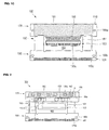
- FIGS. 1A, 1B , and 1C a top plan view, a side elevational view, and a bottom plan view of a flexible circuit board of a liquid crystal display having a light absorbing layer according to aspects of the present invention are illustrated, respectively.
- FIG. 2 a flexible circuit board of a liquid crystal display having a light absorbing layer before mounting a light source is illustrated in the top plan view.
- a flexible circuit board 100 includes a first insulating film 110, a conductive pattern 120, a second insulating film 130, a light source 140, a passive element 150, and a light absorbing layer 160.
- the first insulating film 110 is a base layer, and may be formed with any one selected from flexible polyimide and the equivalent thereof, but the material is not restricted thereto.
- the conductive pattern or patterns 120 are formed on the first insulating film 110.
- the conductive pattern 120 may be formed with any one selected from a high conductive copper thin film and the equivalent thereof, but the material is not restricted thereto.
- the conductive pattern 120 provides power and electrical signals to all sorts of electronic components that may be electrically coupled to the flexible circuit board 100.
- the conductive pattern 120 provides power to the light source 140 or provides an electrical signal to the passive element 150. Only some of conductive patterns 120 are illustrated in FIGS. 1A and 2 , however, several tens to thousands of these conductive patterns 120 may be formed. In the aspect shown, the conductive patterns 120 are not readily visible because the second insulating film 130 is almost opaque.
- the second insulating film 130 is formed on the first insulating film 110 and covers the conductive pattern 120. Therefore, the second insulating film 130 prevents the conductive pattern 120 from being exposed to the outside and being damaged.
- the second insulating film 130 is not formed on parts of the conductive pattern 120 to which the light source 140 and the passive element 150 are to be electrically coupled.
- the second insulating film 130 may be any one selected from a flexible cover film and the equivalent thereof, but the material is not restricted thereto.
- the light source 140 may be electrically coupled to the conductive pattern 120. Substantially, a conductive pad 120a is formed on the conductive pattern 120, and the conductive pad 120a is exposed to the outside of (or exposed through) the second insulating film 130. Therefore, the light source 140 may be electrically coupled to the conductive pad 120a by soldering and/or similar or other attaching or bonding technique.
- the light source 140 may be any one selected from the high-brightness light emitting diode and the equivalent thereof, but the device is not restricted thereto. Three light sources 140 arranged in a row are illustrated in the drawing. However, the number of the light source 140 is not restricted thereto.
- the passive element 150 may be also electrically coupled to the conductive pattern 120. Specifically, a conductive pad 120b (shown in FIG. 5 ) is formed on the conductive pattern 120, and the conductive pad 120b is exposed to the outside of (or exposed through) the second insulating film 130. Therefore, the passive element 150 may be electrically coupled to the conductive pad 120b by soldering and/or similar or other attaching or bonding technique.
- the passive element 150 may be a resistor, a capacitor and/or an inductor or other similar or other passive elements. Accordingly, the kind of the passive element 150 is not restricted thereto. As shown, seven of the passive elements 150 are arranged in a row as illustrated in the drawing. However, the number of the passive elements 150 is not restricted thereto.
- the light absorbing layer 160 includes a first light absorbing layer 161 formed on the first insulating film 110, and a second light absorbing layer 162 formed on the second insulating film 130.
- the first light absorbing layer 161 is formed on the first insulating film 110 which is opposite to the surface on which the light source 140 and the passive element 150 are formed.
- the second light absorbing layer 162 is formed on the second insulating film 130 corresponding to a peripheral portion of (or an area adjacent) the light source 140.
- the second light absorbing layer 162 is spaced apart from the conductive pad 120a so that the light source 140 is electrically coupled to the conductive pad 120a with ease.
- a window 163 is formed in the second light absorbing layer 162, and the conductive pad 120a is exposed to the outside through the window 163.
- the size of the window 163 is slightly greater than that of the conductive pad 120a. Therefore, the light from the light source 140 is hardly (or not readily) transmitted to the conductive pattern 120 and the passive element 150 due to the second light absorbing layer 162. That is, the light from the light source 140 is transmitted only to a light guide plate, which is not depicted in the drawings, and the light is not transmitted to the conductive pattern 120 and the passive element 150.
- a flow of light into the conductive pattern and the passive elements of the inventive flexible circuit board of a liquid crystal display is prevented by the first light absorbing layer together or in conjunction with the second light absorbing layer.
- the first light absorbing layer is provided such that it absorbs light which flows into windows formed within the second light absorbing layer or the outside or circumference of the second light absorbing layer.
- the light absorbing layer 160 may be one selected from a compound consisting of diethylene glycol monoethyl ether acetate (DCAC) (C 8 H 16 O 4 ), titanium dioxide (TiO 2 ) and/or epoxy resin and the equivalent thereof.
- DCAC diethylene glycol monoethyl ether acetate
- TiO 2 titanium dioxide
- epoxy resin epoxy resin
- the material of the light absorbing layer 160 is not restricted thereto.
- the light absorbing layer 160 having the above described structure is referred to as black silk due to the black color. Further, the light absorbing layer 160 absorbs the light from the light source 140 more efficiently, since the light absorbing layer 160 is black.
- the light absorbing layer 160 may be formed by any one method selected from screen printing, photo-lithography and the equivalent thereof. However, the formation method thereof is not restricted thereto.
- the light absorbing layer 160 may be formed by electroless plating and/or electroplating, and it may be formed by coating a black polymer resin, or any combinations thereof.
- the flexible circuit board 100 of the liquid crystal display may be divided into a first region 170, a second region 180 and a third region 190 as shown in FIG. 2 , for example.
- the first insulating film 110 is divided into the first region 170, the second region 180, and the third region 190.
- the first region 170 is the region in which the light source 140, the passive element 150, and the light absorbing layer 160 are formed.
- the first light absorbing layer 161 of the light absorbing layer 160 may be formed in the entire area of the first insulating film 110 corresponding to the first region 170.
- the second light absorbing layer 162 of the light absorbing layer 160 may be partially formed in the area of the second insulating film 130. That is, the second light absorbing layer 162 is only formed on a portion of the second insulating film 130 comprising the light source 140 and is not formed on a portion of the second insulating film 130 comprising the passive element 150. Therefore, the size of the first light absorbing layer 161 is larger than that of the second light absorbing layer 162.
- the second region 180 is adjacent to the first region 170, and a panel connector 183 is formed in the second region 180 so that the liquid crystal panel is electrically coupled thereto.
- first cutout portions 181 that are spaced apart at a predetermined distance are formed in the second region 180, and a second cutout portion 182 is formed between the first cutout portions 181 and connects the first cutout portions 181. Therefore, the first cutout portions 181 and the second cutout portion 182 are formed in an "H.” shape (or a block U shape).
- the panel connector 183 that is electrically coupled to the liquid crystal display panel is formed in the cutout region that includes the first cutout portions 181 and the second cutout portion 182.
- a plurality of conductive patterns 120c shown in FIG.
- the reference numeral 185 is an ink layer which is more flexible than the first insulating layer so as to allow the second region 180 to bend or fold with ease. Further, it is preferable, but not required that the ink layer 185 is selected from UV (ultraviolet) curing ink and/or IR (infrared) curing ink. However, the material or the kind of the ink layer 185 is not restricted thereto.
- the ink layer 185 is more flexible than the first insulating layer. Accordingly, it is possible to form a structure that bends more easily and is more resistant to a weakening in a circuit component mounting strength due to the bending of the flexible circuit board 100.
- the ink layer 185 is formed in a portion of the flexible circuit board 100 that lacks the first insulating film 110. Also, in the non-limiting aspect shown, the ink layer 185 is formed in the region 180 between the first cutout portions 181, where various layers are lacking.
- the third region 190 is adjacent to a side of the second region 180 opposed to the first region (170), and a controller connector 191 is formed in the third region 190 so as to connect an external controller (not shown) electrically thereto.
- a plurality of conductive patterns 120d is exposed to the outside via the first insulating film 110 and the second insulating film 130.
- Fixing holes 199a, 199b may be further formed at the respective corresponding position of the first region 170 and the third region 190. These fixing holes 199a, 199b fix the flexible circuit board 100 in a molding frame (not shown) as the flexible circuit board 100 is connected to a fixing protrusion (not shown) of the molding frame.
- the flexible circuit board 100 may be divided into the first region 170, the second region 180 and the third region 190.
- the light source 140 is electrically coupled to the conductive pad 120a formed on the conductive pattern 120.
- the passive element 150 is electrically coupled to the conductive pad 120b formed on the conductive pattern 120.
- the first light absorbing layer 161 is formed on the surface of the first insulating film 110.
- the second light absorbing layer 162 is formed on the surface of the second insulating film 130.
- the second light absorbing layer 162 has the window 163 formed at the periphery of the conductive pad 120a so that the light source 140 is electrically coupled to the conductive pad 120a without hindrance.
- the light from the light source 140 is not transmitted to the conductive pattern 120, and the passive element 150 via the conductive pattern 120.
- the second light absorbing layer 162 is not formed in the region corresponding to the passive element 150.
- the panel connector 183 is formed in the second region 180, and the conductive pad 120c formed on the conductive pattern 120 is exposed to the outside.
- the ink layer 185 which is more flexible than the first insulating layer, is formed in the second region 180 so that the bending (or folding) thereof is executed with ease.
- the ink layer 185 is selected from a UV (ultraviolet) curing ink and/or an IR (infrared) curing ink, but the kind of the ink layer is not restricted thereto.
- the controller connector 191 is formed in the third region. In the controller connector 191, the conductive pad 120d formed on the conductive pattern 120 is exposed to the outside.
- the light source 140 such as the high-brightness light emitting diode, is mounted at a predetermined interval on the flexible circuit board 100.
- the respective light source 140 is supplied with power via the conductive pad 120a and the conductive pattern 120.
- the respective light source 140 is electrically coupled to the conductive pad 120a formed on the conductive pattern 120 by soldering, or other methods.
- the light from the light source 140 is hardly transmitted to the conductive pattern 120 since the first light absorbing layer 161 is formed on the surface of the first insulating film 110 and the second light absorbing layer 162 is formed on the surface of the second insulating film 130.
- FIG. 5 a cross-sectional view of line 5-5 of FIG. 1A is depicted therein.
- the passive element or elements 150 such as resistors, capacitors, and/or inductors, are mounted at a predetermined interval on the flexible circuit board 100.
- the respective passive element 150 is supplied with electrical signals through the conductive pad 120b and the conductive pattern 120.
- the respective passive element 150 is electrically coupled to the conductive pad 120b formed on the conductive pattern 120 by soldering or other methods.
- FIG. 6 a cross-sectional view of line 6-6 of FIG. 1A is depicted therein.
- the ink layer 185 instead of the first insulating film 110, is formed on the flexible circuit board 100. That is, the ink layer 185 is adhered to the second insulating film 130 instead of the first insulating film 110. Accordingly, it is possible to bend (or fold) the second region 180. That is, when the panel connector 183 of the second region 180 is bent at a specific angle (or folded) so as to be electrically coupled to the liquid crystal display panel, the bend or the fold in the second region 180 may be damaged by the stress if the ink layer 185 is lacking. Therefore, by forming the ink layer 185 instead of the first insulating film 110 in the second region 180 to be bent, the bend region (or the fold region) absorbs the stress during the bending process and is prevented from being broken.
- FIG. 7 a cross-sectional view of line 7-7 of FIG. 1A is depicted therein.
- the panel connector 183 to which the liquid crystal display panel of the second region 180 is electrically coupled is further formed on the flexible circuit board 100.
- the panel connector 183 may be a plurality of conductive patterns 120c which is substantially exposed to the outside of (or through) the first insulating substrate 110. That is, all sorts of electrical signals are supplied to the liquid crystal display panel via the controller connector 191, as a plurality of conductive patterns 120c are electrically coupled to the liquid crystal display panel.
- the flexible circuit board is applicable to small display devices such as a cellular phone, a PMP (portable multimedia player), a digital camera, and/or similar devices.
- the flexible circuit board of a liquid crystal display minimizes a phenomenon of light from the light source being directed to the conductive pattern and the passive element by having the first and second light absorbing layers formed on a peripheral portion of the light source. Therefore, aspects of the present invention effectively prevent or reduce the malfunction of the passive element as well as the malfunction of the liquid crystal panel.
- the flexible circuit board of a liquid crystal display having a light absorbing layer prevents or reduces the light from the light source from being directed to the undesired area (for example, the area in which a driver IC (integrated circuit) to drive the liquid crystal panel is positioned). Accordingly, the image quality of the liquid crystal display is improved.
- the flexible circuit board of a liquid crystal display has the light source and passive element formed in the first region, and has the panel connector electrically coupled to the liquid crystal display panel formed in the second region, and has the controller connector connected to the external controller formed in the third region. Accordingly, it is possible to electrically connect a large number of parts to each other in a minimum of an area efficiently. Accordingly, the flexible circuit board according to an aspect of the present invention can be readily applicable to slim and lightweight portable displays.
- a flow of light into the conductive pattern and the passive elements of the inventive flexible circuit board of a liquid crystal display is prevented by a first light absorbing layer together or in conjunction with a second light absorbing layer. That is, the first light absorbing layer is provided such that it absorbs light which flows into the windows formed within the second light absorbing layer or the outside or circumference of the second light absorbing layer.
- the flexible circuit board of a liquid crystal display may reduce or resist the weakening of the circuit component mounting strength due to the bending of the circuit board by having the ink layer instead of the first insulating film formed in the second region.
Landscapes
- Physics & Mathematics (AREA)
- Nonlinear Science (AREA)
- Microelectronics & Electronic Packaging (AREA)
- Engineering & Computer Science (AREA)
- Optics & Photonics (AREA)
- General Physics & Mathematics (AREA)
- Crystallography & Structural Chemistry (AREA)
- Chemical & Material Sciences (AREA)
- Mathematical Physics (AREA)
- Liquid Crystal (AREA)
- Structure Of Printed Boards (AREA)
- Non-Metallic Protective Coatings For Printed Circuits (AREA)
- Structures For Mounting Electric Components On Printed Circuit Boards (AREA)
- Combinations Of Printed Boards (AREA)
Abstract
Description
- This application claims the benefit of
Korean Application No. 2007-790, filed January 3, 2007 - Aspects of the present invention relate to a flexible circuit board of a liquid crystal display, and more particularly to a flexible circuit board of a liquid crystal display having a light absorbing layer.
- In general, a liquid crystal display is one of several flat display devices to display an image. The liquid crystal display displays an image by use of a liquid crystal. The liquid crystal display is advantageous in that it is thinner and lighter than other display devices, and that it has low driving voltage and low power consumption. Accordingly, liquid crystal display displays are used widely in industrial applications.
- The liquid crystal display includes a thin film transistor (TFT) substrate, a color filter substrate disposed opposite to the thin film transistor substrate, and a liquid crystal display panel composed of a liquid crystal, which is disposed between the thin film transistor substrate and the color filter substrate, and which changes the transmission amount of light as an electrical signal is applied thereto. Additionally, a driving module, which applies an electrical signal to the liquid crystal display panel, is electrically coupled to the liquid crystal display. For this end, a flexible circuit board is disposed between the liquid crystal display panel and the driving module.
- Since the liquid crystal that is included in the liquid crystal display panel does not emit light by itself, the liquid crystal display requires a light source that provides light having a predetermined brightness or above to the liquid crystal display panel so as to display an image.
- A high-brightness light emitting diode has recently come into use in small display devices such as a cellular phone, a PMP (portable multimedia player) and/or a digital camera as a light source to reduce the thickness and weight thereof. For example, such a light source is electrically coupled to the flexible circuit board, and the light from the light source is transmitted to a light guide plate disposed in the rear surface of the liquid crystal display panel.
- The light from the light source that is mounted on the flexible circuit board has to be directed to the light guide plate. However, some of the light is not transmitted to the light guide plate but is transmitted to undesired areas of the flexible circuit board. For example, the flexible circuit board has a conductive pattern formed thereon and passive elements such as resistors or capacitors that are mounted on the flexible circuit board. However, the light from the light source is undesirably transmitted to the conductive pattern and the passive elements.
- Since the light from the light source carries energy of a predetermined intensity, the energy affects the conductive pattern and the passive elements, and the conductive pattern and the passive elements malfunction. Therefore, although the structure in which the light source is mounted on the flexible circuit board is a technique that is necessary to meet the recent trend towards slim and lightweight devices, the reliability of the technique when applied to such devices may be reduced by the malfunctions of the various passive elements.
- Aspects of the present invention are related to overcoming the foregoing and other problems, and an aspect of the present invention is to provide a flexible circuit board of a liquid crystal display having a light absorbing layer so that the light from the light source is not transmitted to the conductive pattern and the passive element, and other benefits.
- To achieve the above described and/or other aspects, a flexible circuit board of a liquid crystal display having a light absorbing layer according to an aspect of the present invention includes a first insulating film having an ink layer, one or more conductive patterns formed on the first insulating film, a second insulating film formed on the first insulating film and covering the one or more conductive patterns, at least one light source which is electrically coupled to the one or more conductive patterns and one or more light absorbing layers formed on an outer circumference of the light source to absorb light from the light source.
- Preferably, the ink layer is formed in a bend of the first insulating film, and the ink layer may be easier to bend than the first insulating film. The ink layer may be a UV curing ink and/or an IR curing ink.
- Preferably, the light absorbing layer may include a first light absorbing layer formed on the surface of the first insulating film, and a second light absorbing layer formed on the surface of the second insulating film.
- Preferably, a window may be formed in the second light absorbing layer so that the one or more conductive patterns to which the light source is electrically coupled is exposed.
- Preferably, a window may be formed in the second light absorbing layer so to expose a portion of the conductive patterns, to which the at least one light source is electrically coupled.
- Preferably, the one or more dimensions of the window may be greater than that of the one or more conductive patterns.
- Preferably, the surface area of the window is greater than that of the portion of the conductive patterns, to which the at least one light source is electrically coupled.
- Preferably, the dimensions of the first light absorbing layer may be greater than that of the second light absorbing layer.
- Preferably, at least one passive element electrically coupled to portions of the one or more conductive patterns may be formed on the outer circumference of the second light absorbing layer.
- Preferably, the first light absorbing layer may be formed on the first insulating film to correspond to the passive element.
- Preferably, the light absorbing layer may include diethylene glycol monoethyl ether acetate, titanium dioxide and/or epoxy resin.
- Preferably, the light source may be a light emitting diode.
- Preferably, the first insulating film may include a first region in which the light source and the light absorbing layers are formed, a second region which is formed on (or to) one side of the first region and electrically coupled to the liquid crystal display panel, and a third region which is formed on (or to) one side of the second region and electrically coupled to an external controller.
- Preferably, first cutout portions are symmetrically formed in the second region spaced apart from each other and a second cutout portion is formed between the first cutout portions. A panel connector electrically coupled to the liquid crystal panel may be formed in the cutout region that includes the first and second cutout portions.
- Preferably, the one or more conductive patterns of the panel connection unit may be exposed through the first insulating film.
- Preferably, a controller connector electrically coupled to the external controller may be formed in the third region.
- Preferably, the one or more conductive patterns of the controller connector may be exposed through the first insulating film.
- Preferably, in the first and third regions, fixing holes may be formed at the respective corresponding positions.
- The flexible circuit board of a liquid crystal display according to aspects of the present invention minimizes the effect of the light from the light source that is directed to the one or more conductive patterns and the passive element by having the first and second light absorbing layers be formed on the outer circumference of the light source. Therefore, an aspect of the present invention prevents or reduces the malfunction of the passive element as well as the malfunction of the liquid crystal panel, effectively.
- The flexible circuit board of a liquid crystal display according to an aspect of the present invention has the light source and passive element formed in the first region, and the panel connector electrically coupled to the liquid crystal display panel formed in the second region, and the controller connector connected to the external controller formed in the third region. Accordingly, it is possible to electrically connect a large number of parts to each other in a minimum of an area efficiently. Accordingly, a flexible circuit board according to aspects of the present invention can be readily applicable to slim and lightweight portable displays.
- The flexible circuit board of a liquid crystal display including the light absorbing layers according to an aspect of the present invention prevents or reduces the light from the light source from being transmitted to undesired areas (for example, the area in which a driver IC (integrated circuit) to drive the liquid crystal panel is positioned). Accordingly, the image quality of the liquid crystal display is improved.
- According to the flexible circuit board of a liquid crystal display according to an aspect of the present invention, the first, second and third regions include the first insulating film and second Insulating film. Therefore, it is easy to fold the desired region, and easy to apply the flexible circuit board to the portable display device that may need a multitude of bends therein.
- The flexible circuit board of a liquid crystal display according to an aspect of the present invention may resist the weakening in the circuit component mounting strength due to the bending of the circuit board by having the ink layer instead of the first insulating film formed in the second region.
- According to an aspect of the present invention, a flexible circuit board of a liquid crystal display includes a first insulating film, one or more conductive patterns formed on the first insulating film, a second insulating film formed on the first insulating film and covering the one or more conductive patterns, at least one light source which is electrically coupled to the one or more conductive patterns, one or more light absorbing layers formed on the outer circumference of the at least one light source to absorb light from the light source, and an ink layer formed over the second insulating film and the one or more conductive patterns at a portion of the flexible circuit board that lacks the first insulating film.
- Additional aspects and/or advantages of the invention will be set forth in part in the description which follows and, in part, will be obvious from the description, or may be learned by practice of the invention.
- These and/or other aspects and advantages of the invention will become apparent and more readily appreciated from the following description of the aspects, taken in conjunction with the accompanying drawings of which:
-
FIGS. 1A, 1B , and1C are a top plan view, a side elevational view, and a bottom plan view, respectively, illustrating a flexible circuit board of a liquid crystal display having a light absorbing layer. -
FIG. 2 is a top plan view illustrating a flexible circuit board of a liquid crystal display having a light absorbing layer before mounting a light source. -
FIG. 3 is a cross-sectional view of line 3-3 ofFIG. 1 . -
FIG. 4 is a cross-sectional view of line 4-4 ofFIG. 1 . -
FIG. 5 is a cross-sectional view of line 5-5 ofFIG. 1 . -
FIG. 6 is a cross-sectional view of line 6-6 ofFIG. 1 . -
FIG. 7 is a cross-sectional view of line 7-7 ofFIG. 1 . - Reference will now be made in detail to the various aspects of the present invention, examples of which are illustrated in the accompanying drawings, wherein like reference numerals refer to the like elements throughout. The aspects are described below in order to explain the present invention by referring to the figures.
- Referring to
FIGS. 1A, 1B , and1C , a top plan view, a side elevational view, and a bottom plan view of a flexible circuit board of a liquid crystal display having a light absorbing layer according to aspects of the present invention are illustrated, respectively. Referring toFIG. 2 , a flexible circuit board of a liquid crystal display having a light absorbing layer before mounting a light source is illustrated in the top plan view. - As shown in
FIGS. 1A, 1B, 1C , andFIG. 2 , aflexible circuit board 100 includes a firstinsulating film 110, aconductive pattern 120, a secondinsulating film 130, alight source 140, apassive element 150, and a lightabsorbing layer 160. - In the non-limiting aspect shown, the first insulating
film 110 is a base layer, and may be formed with any one selected from flexible polyimide and the equivalent thereof, but the material is not restricted thereto. - In the non-limiting aspect shown, the conductive pattern or
patterns 120 are formed on the first insulatingfilm 110. Theconductive pattern 120 may be formed with any one selected from a high conductive copper thin film and the equivalent thereof, but the material is not restricted thereto. Theconductive pattern 120 provides power and electrical signals to all sorts of electronic components that may be electrically coupled to theflexible circuit board 100. For example, theconductive pattern 120 provides power to thelight source 140 or provides an electrical signal to thepassive element 150. Only some ofconductive patterns 120 are illustrated inFIGS. 1A and2 , however, several tens to thousands of theseconductive patterns 120 may be formed. In the aspect shown, theconductive patterns 120 are not readily visible because the secondinsulating film 130 is almost opaque. - In the non-limiting aspect shown, the second
insulating film 130 is formed on the first insulatingfilm 110 and covers theconductive pattern 120. Therefore, the secondinsulating film 130 prevents theconductive pattern 120 from being exposed to the outside and being damaged. The secondinsulating film 130 is not formed on parts of theconductive pattern 120 to which thelight source 140 and thepassive element 150 are to be electrically coupled. The secondinsulating film 130 may be any one selected from a flexible cover film and the equivalent thereof, but the material is not restricted thereto. - In the non-limiting aspect shown, the
light source 140 may be electrically coupled to theconductive pattern 120. Substantially, aconductive pad 120a is formed on theconductive pattern 120, and theconductive pad 120a is exposed to the outside of (or exposed through) the secondinsulating film 130. Therefore, thelight source 140 may be electrically coupled to theconductive pad 120a by soldering and/or similar or other attaching or bonding technique. Thelight source 140 may be any one selected from the high-brightness light emitting diode and the equivalent thereof, but the device is not restricted thereto. Threelight sources 140 arranged in a row are illustrated in the drawing. However, the number of thelight source 140 is not restricted thereto. - In the non-limiting aspect shown, the
passive element 150 may be also electrically coupled to theconductive pattern 120. Specifically, aconductive pad 120b (shown inFIG. 5 ) is formed on theconductive pattern 120, and theconductive pad 120b is exposed to the outside of (or exposed through) the secondinsulating film 130. Therefore, thepassive element 150 may be electrically coupled to theconductive pad 120b by soldering and/or similar or other attaching or bonding technique. In the non-limiting aspect shown, thepassive element 150 may be a resistor, a capacitor and/or an inductor or other similar or other passive elements. Accordingly, the kind of thepassive element 150 is not restricted thereto. As shown, seven of thepassive elements 150 are arranged in a row as illustrated in the drawing. However, the number of thepassive elements 150 is not restricted thereto. - In the non-limiting aspect shown, the
light absorbing layer 160 includes a firstlight absorbing layer 161 formed on the first insulatingfilm 110, and a secondlight absorbing layer 162 formed on the secondinsulating film 130. The firstlight absorbing layer 161 is formed on the first insulatingfilm 110 which is opposite to the surface on which thelight source 140 and thepassive element 150 are formed. The secondlight absorbing layer 162 is formed on the secondinsulating film 130 corresponding to a peripheral portion of (or an area adjacent) thelight source 140. The secondlight absorbing layer 162 is spaced apart from theconductive pad 120a so that thelight source 140 is electrically coupled to theconductive pad 120a with ease. That is, awindow 163 is formed in the secondlight absorbing layer 162, and theconductive pad 120a is exposed to the outside through thewindow 163. The size of thewindow 163 is slightly greater than that of theconductive pad 120a. Therefore, the light from thelight source 140 is hardly (or not readily) transmitted to theconductive pattern 120 and thepassive element 150 due to the secondlight absorbing layer 162. That is, the light from thelight source 140 is transmitted only to a light guide plate, which is not depicted in the drawings, and the light is not transmitted to theconductive pattern 120 and thepassive element 150. Thus, a flow of light into the conductive pattern and the passive elements of the inventive flexible circuit board of a liquid crystal display is prevented by the first light absorbing layer together or in conjunction with the second light absorbing layer. That is, the first light absorbing layer is provided such that it absorbs light which flows into windows formed within the second light absorbing layer or the outside or circumference of the second light absorbing layer. The lightabsorbing layer 160 may be one selected from a compound consisting of diethylene glycol monoethyl ether acetate (DCAC) (C8H16O4), titanium dioxide (TiO2) and/or epoxy resin and the equivalent thereof. However, the material of thelight absorbing layer 160 is not restricted thereto. The lightabsorbing layer 160 having the above described structure is referred to as black silk due to the black color. Further, thelight absorbing layer 160 absorbs the light from thelight source 140 more efficiently, since thelight absorbing layer 160 is black. Furthermore, thelight absorbing layer 160 may be formed by any one method selected from screen printing, photo-lithography and the equivalent thereof. However, the formation method thereof is not restricted thereto. The lightabsorbing layer 160 may be formed by electroless plating and/or electroplating, and it may be formed by coating a black polymer resin, or any combinations thereof. - The
flexible circuit board 100 of the liquid crystal display may be divided into afirst region 170, asecond region 180 and athird region 190 as shown inFIG. 2 , for example. Specifically, the first insulatingfilm 110 is divided into thefirst region 170, thesecond region 180, and thethird region 190. - In the non-limiting aspect shown, the
first region 170 is the region in which thelight source 140, thepassive element 150, and thelight absorbing layer 160 are formed. As shown, the firstlight absorbing layer 161 of thelight absorbing layer 160 may be formed in the entire area of the first insulatingfilm 110 corresponding to thefirst region 170. The secondlight absorbing layer 162 of thelight absorbing layer 160 may be partially formed in the area of the secondinsulating film 130. That is, the secondlight absorbing layer 162 is only formed on a portion of the secondinsulating film 130 comprising thelight source 140 and is not formed on a portion of the secondinsulating film 130 comprising thepassive element 150. Therefore, the size of the firstlight absorbing layer 161 is larger than that of the secondlight absorbing layer 162. - The
second region 180 is adjacent to thefirst region 170, and apanel connector 183 is formed in thesecond region 180 so that the liquid crystal panel is electrically coupled thereto. For this end,first cutout portions 181 that are spaced apart at a predetermined distance are formed in thesecond region 180, and asecond cutout portion 182 is formed between thefirst cutout portions 181 and connects thefirst cutout portions 181. Therefore, thefirst cutout portions 181 and thesecond cutout portion 182 are formed in an "H." shape (or a block U shape). Thepanel connector 183 that is electrically coupled to the liquid crystal display panel is formed in the cutout region that includes thefirst cutout portions 181 and thesecond cutout portion 182. A plurality ofconductive patterns 120c (shown inFIG. 1C ) are exposed to the outside through the first insulatingfilm 110. InFIG. 1C , thereference numeral 185 is an ink layer which is more flexible than the first insulating layer so as to allow thesecond region 180 to bend or fold with ease. Further, it is preferable, but not required that theink layer 185 is selected from UV (ultraviolet) curing ink and/or IR (infrared) curing ink. However, the material or the kind of theink layer 185 is not restricted thereto. Theink layer 185 is more flexible than the first insulating layer. Accordingly, it is possible to form a structure that bends more easily and is more resistant to a weakening in a circuit component mounting strength due to the bending of theflexible circuit board 100. In the non-limiting aspect shown, theink layer 185 is formed in a portion of theflexible circuit board 100 that lacks the first insulatingfilm 110. Also, in the non-limiting aspect shown, theink layer 185 is formed in theregion 180 between thefirst cutout portions 181, where various layers are lacking. - In the non-limiting aspect shown, the
third region 190 is adjacent to a side of thesecond region 180 opposed to the first region (170), and acontroller connector 191 is formed in thethird region 190 so as to connect an external controller (not shown) electrically thereto. As shown, a plurality ofconductive patterns 120d is exposed to the outside via the first insulatingfilm 110 and the secondinsulating film 130. Additionally, Fixingholes first region 170 and thethird region 190. These fixingholes flexible circuit board 100 in a molding frame (not shown) as theflexible circuit board 100 is connected to a fixing protrusion (not shown) of the molding frame. - Referring
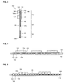
FIG. 3 , a cross-sectional view of line 3-3 ofFIG. 1A is described therein. As shown inFIG. 3 , theflexible circuit board 100 may be divided into thefirst region 170, thesecond region 180 and thethird region 190. - In the
first region 170, thelight source 140 is electrically coupled to theconductive pad 120a formed on theconductive pattern 120. Thepassive element 150 is electrically coupled to theconductive pad 120b formed on theconductive pattern 120. In thefirst region 170, the firstlight absorbing layer 161 is formed on the surface of the first insulatingfilm 110. In thefirst region 170, the secondlight absorbing layer 162 is formed on the surface of the secondinsulating film 130. Here, the secondlight absorbing layer 162 has thewindow 163 formed at the periphery of theconductive pad 120a so that thelight source 140 is electrically coupled to theconductive pad 120a without hindrance. By way of this structure, the light from thelight source 140 is not transmitted to theconductive pattern 120, and thepassive element 150 via theconductive pattern 120. Also, the secondlight absorbing layer 162 is not formed in the region corresponding to thepassive element 150. - The
panel connector 183 is formed in thesecond region 180, and theconductive pad 120c formed on theconductive pattern 120 is exposed to the outside. Theink layer 185, which is more flexible than the first insulating layer, is formed in thesecond region 180 so that the bending (or folding) thereof is executed with ease. Theink layer 185 is selected from a UV (ultraviolet) curing ink and/or an IR (infrared) curing ink, but the kind of the ink layer is not restricted thereto. - The
controller connector 191 is formed in the third region. In thecontroller connector 191, theconductive pad 120d formed on theconductive pattern 120 is exposed to the outside. - Referring to
FIG. 4 , a cross-sectional view of line 4-4 ofFIG. 1A is depicted therein. As shown inFIG. 4 , thelight source 140, such as the high-brightness light emitting diode, is mounted at a predetermined interval on theflexible circuit board 100. The respectivelight source 140 is supplied with power via theconductive pad 120a and theconductive pattern 120. The respectivelight source 140 is electrically coupled to theconductive pad 120a formed on theconductive pattern 120 by soldering, or other methods. The light from thelight source 140 is hardly transmitted to theconductive pattern 120 since the firstlight absorbing layer 161 is formed on the surface of the first insulatingfilm 110 and the secondlight absorbing layer 162 is formed on the surface of the secondinsulating film 130. - Referring to
FIG. 5 , a cross-sectional view of line 5-5 ofFIG. 1A is depicted therein. - As shown in the drawing, the passive element or
elements 150, such as resistors, capacitors, and/or inductors, are mounted at a predetermined interval on theflexible circuit board 100. The respectivepassive element 150 is supplied with electrical signals through theconductive pad 120b and theconductive pattern 120. The respectivepassive element 150 is electrically coupled to theconductive pad 120b formed on theconductive pattern 120 by soldering or other methods. - Referring to
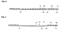
FIG. 6 , a cross-sectional view of line 6-6 ofFIG. 1A is depicted therein. - As shown in
FIG. 6 , in thesecond region 180, theink layer 185, instead of the first insulatingfilm 110, is formed on theflexible circuit board 100. That is, theink layer 185 is adhered to the secondinsulating film 130 instead of the first insulatingfilm 110. Accordingly, it is possible to bend (or fold) thesecond region 180. That is, when thepanel connector 183 of thesecond region 180 is bent at a specific angle (or folded) so as to be electrically coupled to the liquid crystal display panel, the bend or the fold in thesecond region 180 may be damaged by the stress if theink layer 185 is lacking. Therefore, by forming theink layer 185 instead of the first insulatingfilm 110 in thesecond region 180 to be bent, the bend region (or the fold region) absorbs the stress during the bending process and is prevented from being broken. - Referring to
FIG. 7 , a cross-sectional view of line 7-7 ofFIG. 1A is depicted therein. As shown inFIG. 7 , thepanel connector 183 to which the liquid crystal display panel of thesecond region 180 is electrically coupled is further formed on theflexible circuit board 100. Thepanel connector 183 may be a plurality ofconductive patterns 120c which is substantially exposed to the outside of (or through) the first insulatingsubstrate 110. That is, all sorts of electrical signals are supplied to the liquid crystal display panel via thecontroller connector 191, as a plurality ofconductive patterns 120c are electrically coupled to the liquid crystal display panel. - In various aspects, the flexible circuit board is applicable to small display devices such as a cellular phone, a PMP (portable multimedia player), a digital camera, and/or similar devices.
- As described above, the flexible circuit board of a liquid crystal display according to aspects of the present invention minimizes a phenomenon of light from the light source being directed to the conductive pattern and the passive element by having the first and second light absorbing layers formed on a peripheral portion of the light source. Therefore, aspects of the present invention effectively prevent or reduce the malfunction of the passive element as well as the malfunction of the liquid crystal panel.
- The flexible circuit board of a liquid crystal display having a light absorbing layer according to aspects of the present invention prevents or reduces the light from the light source from being directed to the undesired area (for example, the area in which a driver IC (integrated circuit) to drive the liquid crystal panel is positioned). Accordingly, the image quality of the liquid crystal display is improved.
- The flexible circuit board of a liquid crystal display according to an aspect of the present invention has the light source and passive element formed in the first region, and has the panel connector electrically coupled to the liquid crystal display panel formed in the second region, and has the controller connector connected to the external controller formed in the third region. Accordingly, it is possible to electrically connect a large number of parts to each other in a minimum of an area efficiently. Accordingly, the flexible circuit board according to an aspect of the present invention can be readily applicable to slim and lightweight portable displays.
- According to an aspect of the invention a flow of light into the conductive pattern and the passive elements of the inventive flexible circuit board of a liquid crystal display is prevented by a first light absorbing layer together or in conjunction with a second light absorbing layer. That is, the first light absorbing layer is provided such that it absorbs light which flows into the windows formed within the second light absorbing layer or the outside or circumference of the second light absorbing layer.
- The flexible circuit board of a liquid crystal display according to aspects of the present invention may reduce or resist the weakening of the circuit component mounting strength due to the bending of the circuit board by having the ink layer instead of the first insulating film formed in the second region.
- Although a few aspects of the present invention have been shown and described, it would be appreciated by those skilled in the art that changes may be made in the aspects without departing from the principles of the invention, the scope of which is defined in the claims and their equivalents.
Claims (16)
- A flexible circuit board (100) for a liquid crystal display, comprising:a first insulating film (110) comprising an ink layer (185);a plurality of conductive patterns (120) formed on the first insulating film (110);a second insulating film (130) formed on the first insulating film (110) and covering the conductive patterns (120);at least one light source (140) which is electrically coupled to the conductive patterns (120);a second light absorbing layer (162) formed on a surface of the second insulating film (130) in a peripheral portion of the at least one light source (140) for absorbing light from the light source (140).
- The flexible circuit board for a liquid crystal display as claimed in claim 1, wherein the ink layer (185) replaces a portion of the first insulating film (110).
- The flexible circuit board for a liquid crystal display as claimed in one of the preceding claims, wherein the ink layer (185) is more flexible than the first insulating film (110).
- The flexible circuit board for a liquid crystal display as claimed in one of the preceding claims, wherein the ink layer (185) is a UV curing ink and/or an IR curing ink.
- The flexible circuit board of a liquid crystal display as claimed in one of the preceding claims, further comprising a first light absorbing layer (161) formed on a surface of the first insulating film (110).
- The flexible circuit board for a liquid crystal display as claimed in claim 5, wherein a surface area of the first light absorbing layer (161) is larger than a surface area of the second light absorbing layer (162).
- The flexible circuit board for a liquid crystal display as claimed in one of the preceding claims, further comprising at least one passive element (150) which is electrically coupled to a portion (120b) of the conductive patterns (120) and is formed on the second insulating film (130) adjacent to the second light absorbing layer (162).
- The flexible circuit board for a liquid crystal display as claimed in claim 7, wherein the first light absorbing layer (161) is formed on a portion of the first insulating film (110) corresponding to the at least one passive element (150).
- The flexible circuit board of a liquid crystal display as claimed in one of the preceding claims, wherein the first and/or the second light absorbing layers (161, 162) include diethylene glycol monoethyl ether acetate, titanium dioxide, epoxy resin, or any combinations thereof.
- The flexible circuit board for a liquid crystal display as claimed in one of the preceding claims, wherein the at least one light source (140) is a light emitting diode.
- A liquid crystal display comprising:a flexible circuit board as claimed in one of the claims 1 through 12; and an external controller;wherein the first insulating film (110) includes:a first region (170) in which the at least one light source (140) and the light absorbing layers (161, 162) are formed;a second region (180) adjacent to the first region (170) and being electrically coupled to a liquid crystal display panel; anda third region (190) adjacent to one side of the second region (180) opposed to the first region (170) and being electrically coupled to the external controller.
- The liquid crystal display as claimed in claim 11,
the flexible circuit board further comprising:a cutout region including first cutout portions (181) and a second cutout portion (182); anda panel connector (183),wherein the first cutout portions (181) are spaced apart from each other and are symmetrically formed in the second region (180), and the second cutout portion (182) is formed between the first cutout portions (181), and the panel connector (183) is formed in the cutout region and is electrically coupled to the liquid crystal panel. - The liquid crystal display as claimed in claim 12, wherein the panel connector (183) includes portions (120c) of the conductive patterns (120) that are exposed through the first insulating film (110).
- The liquid crystal display as claimed in claim 11, wherein the third region (190) includes a controller connector (191) adapted to be electrically coupled to the external controller.
- The liquid crystal display as claimed in claim 14, wherein the controller connector (191) includes portions (120d) of the conductive patterns (120) that are exposed through the first insulating film (110).
- The flexible circuit board of a liquid crystal display as claimed in claim 12, further comprising fixing holes formed at respective corresponding positions in the first and third regions.
Applications Claiming Priority (1)
| Application Number | Priority Date | Filing Date | Title |
|---|---|---|---|
| KR1020070000790A KR100788556B1 (en) | 2007-01-03 | 2007-01-03 | Flexible circuit board for liquid crystal display device having light absorption layer |
Publications (2)
| Publication Number | Publication Date |
|---|---|
| EP1942708A1 true EP1942708A1 (en) | 2008-07-09 |
| EP1942708B1 EP1942708B1 (en) | 2009-07-29 |
Family
ID=39147959
Family Applications (1)
| Application Number | Title | Priority Date | Filing Date |
|---|---|---|---|
| EP08100061A Not-in-force EP1942708B1 (en) | 2007-01-03 | 2008-01-03 | Flexible circuit board of liquid crystal display having a light absorbing layer |
Country Status (6)
| Country | Link |
|---|---|
| US (1) | US20080158472A1 (en) |
| EP (1) | EP1942708B1 (en) |
| JP (1) | JP4691522B2 (en) |
| KR (1) | KR100788556B1 (en) |
| CN (1) | CN101216617B (en) |
| DE (1) | DE602008000057D1 (en) |
Families Citing this family (8)
| Publication number | Priority date | Publication date | Assignee | Title |
|---|---|---|---|---|
| KR101441428B1 (en) * | 2008-02-18 | 2014-09-17 | 삼성디스플레이 주식회사 | Flexible printed circuit board and display device including the same |
| KR101725999B1 (en) * | 2010-11-04 | 2017-04-11 | 엘지디스플레이 주식회사 | Backlgiht unit and liquid crystal display device the same |
| KR101226936B1 (en) * | 2010-11-10 | 2013-01-30 | 주식회사 엘지화학 | Optical member and method for manufacturing the same and backlight using the optical member, and method for manufacturing the same |
| KR101896703B1 (en) | 2012-02-17 | 2018-10-04 | 리쿠아비스타 비.브이. | Electrowetting display device and manufacturing method thereof |
| TWI509189B (en) * | 2012-06-13 | 2015-11-21 | Innocom Tech Shenzhen Co Ltd | Display and backlight module and lighting module thereof |
| CN103486492B (en) * | 2012-06-13 | 2017-01-18 | 群康科技(深圳)有限公司 | Display and backlight module and light source module thereof |
| US9983455B2 (en) * | 2015-12-22 | 2018-05-29 | Amazon Technologies, Inc. | Electronic device stack assembly |
| CN108111650B (en) * | 2018-01-10 | 2020-07-03 | 北京小米移动软件有限公司 | LCD display module and mobile terminal |
Citations (4)
| Publication number | Priority date | Publication date | Assignee | Title |
|---|---|---|---|---|
| US4439818A (en) * | 1983-02-25 | 1984-03-27 | Scheib Joseph J | Flexible light display with evenly distributed illumination |
| JPH09274446A (en) * | 1996-12-16 | 1997-10-21 | Toshiba Corp | Flexible wiring board manufacturing method |
| US20050190333A1 (en) * | 2004-02-27 | 2005-09-01 | Au Optronics Corp. | Planar display module |
| US20060082297A1 (en) * | 2004-10-19 | 2006-04-20 | Eastman Kodak Company | Method of preparing a lens-less LED |
Family Cites Families (25)
| Publication number | Priority date | Publication date | Assignee | Title |
|---|---|---|---|---|
| JP2978383B2 (en) * | 1993-09-22 | 1999-11-15 | シャープ株式会社 | Display device |
| TW383508B (en) * | 1996-07-29 | 2000-03-01 | Nichia Kagaku Kogyo Kk | Light emitting device and display |
| JPH10123964A (en) * | 1996-08-30 | 1998-05-15 | Sony Corp | Liquid crystal display |
| DE19939076A1 (en) * | 1999-08-18 | 2001-02-22 | Beiersdorf Ag | Packaging tape with natural rubber hot melt pressure sensitive adhesive |
| JP3787753B2 (en) * | 1999-12-28 | 2006-06-21 | ミネベア株式会社 | Surface lighting device |
| US6699351B2 (en) * | 2000-03-24 | 2004-03-02 | 3M Innovative Properties Company | Anisotropically conductive adhesive composition and anisotropically conductive adhesive film formed from it |
| US6896967B2 (en) * | 2000-09-16 | 2005-05-24 | Goo Chemical Co., Ltd. | Ultraviolet-curable resin composition and photosolder resist ink containing the composition |
| DE60327426D1 (en) * | 2002-03-01 | 2009-06-10 | Markem Corp | MARKING OF SUBSTRATES |
| JP2003344851A (en) * | 2002-05-22 | 2003-12-03 | Optrex Corp | Liquid crystal display device |
| JP4386623B2 (en) * | 2002-08-27 | 2009-12-16 | セイコーエプソン株式会社 | Liquid crystal display |
| TWI266092B (en) * | 2002-12-31 | 2006-11-11 | Hon Hai Prec Ind Co Ltd | Light guide plate and back light system with the same |
| JP4543772B2 (en) * | 2003-09-19 | 2010-09-15 | セイコーエプソン株式会社 | Electro-optical device and electronic apparatus |
| TWI222543B (en) * | 2003-09-26 | 2004-10-21 | Au Optronics Corp | Liquid crystal display module (LCM) |
| KR100818749B1 (en) * | 2004-06-14 | 2008-04-04 | 하바텍 코포레이션 | White light emitting diode light source and its manufacturing method |
| KR101097486B1 (en) * | 2004-06-28 | 2011-12-22 | 엘지디스플레이 주식회사 | back light unit of liquid crystal display device |
| TWM263518U (en) * | 2004-07-06 | 2005-05-01 | Au Optronics Corp | Backlight module |
| JP4251129B2 (en) * | 2004-10-25 | 2009-04-08 | セイコーエプソン株式会社 | Mounting structure, electro-optical device, and electronic apparatus |
| JP4552637B2 (en) * | 2004-12-09 | 2010-09-29 | エプソンイメージングデバイス株式会社 | Liquid crystal display |
| US7576805B2 (en) * | 2004-12-22 | 2009-08-18 | Mitsubishi Denki Kabushiki Kaisha | Display device with light guide plate having antireflection portions on light incident surfaces |
| KR100613218B1 (en) * | 2005-02-02 | 2006-08-21 | 럭스피아 주식회사 | LCD module using LED package array |
| KR20060090392A (en) * | 2005-02-07 | 2006-08-10 | 삼성전자주식회사 | Flat panel display for EMI shielding |
| US7284894B2 (en) * | 2005-05-31 | 2007-10-23 | Avago Technologies Eceliip (Singapore) Pte Ltd | Light source utilizing a flexible circuit carrier |
| KR20060126074A (en) * | 2005-06-03 | 2006-12-07 | 삼성전자주식회사 | Backlight assembly with improved heat dissipation structure and display device having same |
| JP2006349789A (en) * | 2005-06-14 | 2006-12-28 | Sanyo Epson Imaging Devices Corp | Optoelectronic apparatus, method for manufacturing optoelectronic apparatus, and electronic apparatus |
| TWI306652B (en) * | 2005-10-28 | 2009-02-21 | Chipmos Technologies Inc | Light emitting diode package structure |
-
2007
- 2007-01-03 KR KR1020070000790A patent/KR100788556B1/en not_active Expired - Fee Related
- 2007-04-19 JP JP2007110951A patent/JP4691522B2/en not_active Expired - Fee Related
- 2007-12-03 US US11/949,201 patent/US20080158472A1/en not_active Abandoned
- 2007-12-29 CN CN2007103016622A patent/CN101216617B/en not_active Expired - Fee Related
-
2008
- 2008-01-03 DE DE602008000057T patent/DE602008000057D1/en active Active
- 2008-01-03 EP EP08100061A patent/EP1942708B1/en not_active Not-in-force
Patent Citations (4)
| Publication number | Priority date | Publication date | Assignee | Title |
|---|---|---|---|---|
| US4439818A (en) * | 1983-02-25 | 1984-03-27 | Scheib Joseph J | Flexible light display with evenly distributed illumination |
| JPH09274446A (en) * | 1996-12-16 | 1997-10-21 | Toshiba Corp | Flexible wiring board manufacturing method |
| US20050190333A1 (en) * | 2004-02-27 | 2005-09-01 | Au Optronics Corp. | Planar display module |
| US20060082297A1 (en) * | 2004-10-19 | 2006-04-20 | Eastman Kodak Company | Method of preparing a lens-less LED |
Also Published As
| Publication number | Publication date |
|---|---|
| CN101216617B (en) | 2010-12-08 |
| US20080158472A1 (en) | 2008-07-03 |
| CN101216617A (en) | 2008-07-09 |
| DE602008000057D1 (en) | 2009-09-10 |
| JP4691522B2 (en) | 2011-06-01 |
| KR100788556B1 (en) | 2007-12-26 |
| EP1942708B1 (en) | 2009-07-29 |
| JP2008166679A (en) | 2008-07-17 |
Similar Documents
| Publication | Publication Date | Title |
|---|---|---|
| EP1942708B1 (en) | Flexible circuit board of liquid crystal display having a light absorbing layer | |
| EP1942709B1 (en) | Flexible circuit board and liquid crystal display having the same | |
| US11337308B2 (en) | Display panel and display apparatus | |
| US20070290965A1 (en) | Liquid crystal display device | |
| US20190122943A1 (en) | Film for package substrate, semiconductor package, display device, and methods of fabricating the film, the semiconductor package, the display device | |
| US8067697B2 (en) | Flexible printed circuit board for light emitting diode backlight unit and method of fabricating the same | |
| CN1598649A (en) | Electrooptical device,flexible wiring substrate,manufacturing method of electrooptical device and electronic device | |
| CN1266283A (en) | Semiconductor device, instllation structure for smeiconductor device, liquid crystal device and electronic device | |
| CN101008753A (en) | Display device | |
| US8593610B2 (en) | Liquid crystal display device | |
| EP1942366B1 (en) | Flexible circuit board having a light absorbing layer for a liquid crystal display | |
| KR102034058B1 (en) | Display device | |
| US20090115054A1 (en) | Electronic component | |
| CN101217852B (en) | Flexible circuit board and liquid crystal display with same | |
| WO2012141117A1 (en) | Liquid crystal module, and display device | |
| KR102378493B1 (en) | Film for package substrate, semiconductor package, display device and methods of fabricating the same | |
| KR100833748B1 (en) | Flexible circuit board for liquid crystal display device having light absorption layer | |
| KR100795666B1 (en) | Liquid crystal display | |
| KR102230736B1 (en) | Printed circuit board and liquid crystal display device ncluding the same | |
| JP5115117B2 (en) | Liquid crystal display | |
| KR20220001771A (en) | Antenna structure and image display device including the same | |
| KR20060080766A (en) | Backlight Assembly and Display Device Using the Same | |
| KR20070032531A (en) | Display device |
Legal Events
| Date | Code | Title | Description |
|---|---|---|---|
| PUAI | Public reference made under article 153(3) epc to a published international application that has entered the european phase |
Free format text: ORIGINAL CODE: 0009012 |
|
| 17P | Request for examination filed |
Effective date: 20080103 |
|
| AK | Designated contracting states |
Kind code of ref document: A1 Designated state(s): AT BE BG CH CY CZ DE DK EE ES FI FR GB GR HR HU IE IS IT LI LT LU LV MC MT NL NO PL PT RO SE SI SK TR |
|
| AX | Request for extension of the european patent |
Extension state: AL BA MK RS |
|
| GRAP | Despatch of communication of intention to grant a patent |
Free format text: ORIGINAL CODE: EPIDOSNIGR1 |
|
| RAP1 | Party data changed (applicant data changed or rights of an application transferred) |
Owner name: SAMSUNG MOBILE DISPLAY CO., LTD. |
|
| AKX | Designation fees paid |
Designated state(s): DE FR GB |
|
| GRAS | Grant fee paid |
Free format text: ORIGINAL CODE: EPIDOSNIGR3 |
|
| GRAA | (expected) grant |
Free format text: ORIGINAL CODE: 0009210 |
|
| AK | Designated contracting states |
Kind code of ref document: B1 Designated state(s): DE FR GB |
|
| REG | Reference to a national code |
Ref country code: GB Ref legal event code: FG4D |
|
| REF | Corresponds to: |
Ref document number: 602008000057 Country of ref document: DE Date of ref document: 20090910 Kind code of ref document: P |
|
| PLBE | No opposition filed within time limit |
Free format text: ORIGINAL CODE: 0009261 |
|
| STAA | Information on the status of an ep patent application or granted ep patent |
Free format text: STATUS: NO OPPOSITION FILED WITHIN TIME LIMIT |
|
| 26N | No opposition filed |
Effective date: 20100503 |
|
| PGFP | Annual fee paid to national office [announced via postgrant information from national office to epo] |
Ref country code: FR Payment date: 20110128 Year of fee payment: 4 Ref country code: DE Payment date: 20101230 Year of fee payment: 4 |
|
| GBPC | Gb: european patent ceased through non-payment of renewal fee |
Effective date: 20120103 |
|
| REG | Reference to a national code |
Ref country code: FR Ref legal event code: ST Effective date: 20120928 |
|
| PG25 | Lapsed in a contracting state [announced via postgrant information from national office to epo] |
Ref country code: DE Free format text: LAPSE BECAUSE OF NON-PAYMENT OF DUE FEES Effective date: 20120801 Ref country code: GB Free format text: LAPSE BECAUSE OF NON-PAYMENT OF DUE FEES Effective date: 20120103 |
|
| REG | Reference to a national code |
Ref country code: DE Ref legal event code: R119 Ref document number: 602008000057 Country of ref document: DE Effective date: 20120801 |
|
| PG25 | Lapsed in a contracting state [announced via postgrant information from national office to epo] |
Ref country code: FR Free format text: LAPSE BECAUSE OF NON-PAYMENT OF DUE FEES Effective date: 20120131 |