EP1942367B1 - Panel type display device - Google Patents
Panel type display device Download PDFInfo
- Publication number
- EP1942367B1 EP1942367B1 EP07118363.6A EP07118363A EP1942367B1 EP 1942367 B1 EP1942367 B1 EP 1942367B1 EP 07118363 A EP07118363 A EP 07118363A EP 1942367 B1 EP1942367 B1 EP 1942367B1
- Authority
- EP
- European Patent Office
- Prior art keywords
- case
- circuit board
- cooling fluid
- fluid path
- display panel
- Prior art date
- Legal status (The legal status is an assumption and is not a legal conclusion. Google has not performed a legal analysis and makes no representation as to the accuracy of the status listed.)
- Ceased
Links
Images


Classifications
-
- G—PHYSICS
- G09—EDUCATION; CRYPTOGRAPHY; DISPLAY; ADVERTISING; SEALS
- G09F—DISPLAYING; ADVERTISING; SIGNS; LABELS OR NAME-PLATES; SEALS
- G09F9/00—Indicating arrangements for variable information in which the information is built-up on a support by selection or combination of individual elements
-
- G—PHYSICS
- G02—OPTICS
- G02F—OPTICAL DEVICES OR ARRANGEMENTS FOR THE CONTROL OF LIGHT BY MODIFICATION OF THE OPTICAL PROPERTIES OF THE MEDIA OF THE ELEMENTS INVOLVED THEREIN; NON-LINEAR OPTICS; FREQUENCY-CHANGING OF LIGHT; OPTICAL LOGIC ELEMENTS; OPTICAL ANALOGUE/DIGITAL CONVERTERS
- G02F1/00—Devices or arrangements for the control of the intensity, colour, phase, polarisation or direction of light arriving from an independent light source, e.g. switching, gating or modulating; Non-linear optics
- G02F1/01—Devices or arrangements for the control of the intensity, colour, phase, polarisation or direction of light arriving from an independent light source, e.g. switching, gating or modulating; Non-linear optics for the control of the intensity, phase, polarisation or colour
- G02F1/13—Devices or arrangements for the control of the intensity, colour, phase, polarisation or direction of light arriving from an independent light source, e.g. switching, gating or modulating; Non-linear optics for the control of the intensity, phase, polarisation or colour based on liquid crystals, e.g. single liquid crystal display cells
- G02F1/133—Constructional arrangements; Operation of liquid crystal cells; Circuit arrangements
- G02F1/1333—Constructional arrangements; Manufacturing methods
- G02F1/133382—Heating or cooling of liquid crystal cells other than for activation, e.g. circuits or arrangements for temperature control, stabilisation or uniform distribution over the cell
- G02F1/133385—Heating or cooling of liquid crystal cells other than for activation, e.g. circuits or arrangements for temperature control, stabilisation or uniform distribution over the cell with cooling means, e.g. fans
-
- G—PHYSICS
- G02—OPTICS
- G02F—OPTICAL DEVICES OR ARRANGEMENTS FOR THE CONTROL OF LIGHT BY MODIFICATION OF THE OPTICAL PROPERTIES OF THE MEDIA OF THE ELEMENTS INVOLVED THEREIN; NON-LINEAR OPTICS; FREQUENCY-CHANGING OF LIGHT; OPTICAL LOGIC ELEMENTS; OPTICAL ANALOGUE/DIGITAL CONVERTERS
- G02F1/00—Devices or arrangements for the control of the intensity, colour, phase, polarisation or direction of light arriving from an independent light source, e.g. switching, gating or modulating; Non-linear optics
- G02F1/01—Devices or arrangements for the control of the intensity, colour, phase, polarisation or direction of light arriving from an independent light source, e.g. switching, gating or modulating; Non-linear optics for the control of the intensity, phase, polarisation or colour
- G02F1/13—Devices or arrangements for the control of the intensity, colour, phase, polarisation or direction of light arriving from an independent light source, e.g. switching, gating or modulating; Non-linear optics for the control of the intensity, phase, polarisation or colour based on liquid crystals, e.g. single liquid crystal display cells
- G02F1/133—Constructional arrangements; Operation of liquid crystal cells; Circuit arrangements
- G02F1/1333—Constructional arrangements; Manufacturing methods
- G02F1/133308—Support structures for LCD panels, e.g. frames or bezels
-
- G—PHYSICS
- G06—COMPUTING OR CALCULATING; COUNTING
- G06F—ELECTRIC DIGITAL DATA PROCESSING
- G06F1/00—Details not covered by groups G06F3/00 - G06F13/00 and G06F21/00
- G06F1/16—Constructional details or arrangements
- G06F1/20—Cooling means
-
- H—ELECTRICITY
- H04—ELECTRIC COMMUNICATION TECHNIQUE
- H04N—PICTORIAL COMMUNICATION, e.g. TELEVISION
- H04N5/00—Details of television systems
- H04N5/64—Constructional details of receivers, e.g. cabinets or dust covers
-
- H—ELECTRICITY
- H04—ELECTRIC COMMUNICATION TECHNIQUE
- H04N—PICTORIAL COMMUNICATION, e.g. TELEVISION
- H04N5/00—Details of television systems
- H04N5/66—Transforming electric information into light information
-
- H—ELECTRICITY
- H05—ELECTRIC TECHNIQUES NOT OTHERWISE PROVIDED FOR
- H05K—PRINTED CIRCUITS; CASINGS OR CONSTRUCTIONAL DETAILS OF ELECTRIC APPARATUS; MANUFACTURE OF ASSEMBLAGES OF ELECTRICAL COMPONENTS
- H05K7/00—Constructional details common to different types of electric apparatus
- H05K7/20—Modifications to facilitate cooling, ventilating, or heating
- H05K7/20954—Modifications to facilitate cooling, ventilating, or heating for display panels
- H05K7/20963—Heat transfer by conduction from internal heat source to heat radiating structure
-
- G—PHYSICS
- G02—OPTICS
- G02F—OPTICAL DEVICES OR ARRANGEMENTS FOR THE CONTROL OF LIGHT BY MODIFICATION OF THE OPTICAL PROPERTIES OF THE MEDIA OF THE ELEMENTS INVOLVED THEREIN; NON-LINEAR OPTICS; FREQUENCY-CHANGING OF LIGHT; OPTICAL LOGIC ELEMENTS; OPTICAL ANALOGUE/DIGITAL CONVERTERS
- G02F2201/00—Constructional arrangements not provided for in groups G02F1/00 - G02F7/00
- G02F2201/36—Airflow channels, e.g. constructional arrangements facilitating the flow of air
Definitions
- the present invention relates to a panel type display device according to the preamble of claim 1 or the preamble of claim 8, and, in particular, to a panel type display device capable of minimizing temperature increase in the interior of a case and a display panel.
- US 6,104,451 discloses a large thin display unit having a chassis structure. An air route is formed between a third enclosure and a planar portion of the second enclosure, and an air route is formed between the thin display section and the planar portion of the second enclosure, see figure 1 .
- TW 266125 discloses a direct type backlight module comprising a back bezel, a light source, a circuit board and a heat insulating element, wherein the circuit board is disposed outside the back bezel.
- a panel type display device such as a Liquid Crystal Display (LCD) or a Plasma Display Panel (PDP), has a flat type panel on which images are displayed.
- the panel type display device has a thinner thickness and a lighter weight as compared with those of a conventional cathode ray tube (CRT) display device.
- CTR cathode ray tube
- such a display device includes a case having front and rear cases, a display panel mounted in an interior of the case, and circuit boards mounted in the interior of the case to be electrically connected to the display panel.
- Air inlets through which air flows are formed at a lower portion of the rear case, and air outlets through which air is exhausted are formed at an upper portion of the rear case. Air flowing through the lower air inlets cools down the display panel and the circuit boards in the interior of the case, and is then exhausted through the upper air outlets.
- a display panel and circuit boards, from which heat is produced are mounted in the same space, such as the interior of a case.
- Such a temperature increase causes the surface temperature of a display panel to be increased.
- the temperature increase causes deterioration of the liquid crystal.
- an aspect of the present invention is to provide a panel type display device capable of minimizing temperature increase in the interior of a case and a display panel.
- the present invention provides a panel display device according to claims 1 or 8.
- the case may include front and rear cases coupled to each other, and the rear case may include a circuit board mounting part provided on an outer surface of the rear case such that the circuit board is mounted in the circuit board mounting part.
- the circuit board mounting part may have an open rear while being recessed from the outer surface of the rear case such that the circuit board is mounted in the circuit board mounting part, and a cover for covering the circuit board mounting part, on which a plurality of air flow holes are formed, may be mounted on the circuit board mounting part.
- the first cooling fluid path may include a space between a rear surface of the display panel and an inner surface of the rear case
- the second cooling fluid path may include an internal space of the circuit board mounting part.
- air inlets through which air flows in the first cooling fluid path may be formed at a lower portion of the rear case, and air outlets through which air is exhausted from the first cooling fluid path may be formed at an upper portion of the rear case.
- a panel type display device which includes: a case; a partition plate for partitioning an interior of the case into first and second cooling fluid paths; a display panel mounted between the partition plate and a front surface of the case to be cooled by air flowing in the first cooling fluid path; and at least one circuit board mounted between the partition plate and a rear surface of the case to be cooled by air flowing in the second cooling fluid path.
- FIGS. 1 and 2 illustrate a panel type display device according to a first embodiment of the present invention.
- the display device includes a case 10, a display panel 20 mounted at an inner front of the case 10, and a plurality of circuit boards 31, 32 and 33 mounted at a rear of the case 10.
- the case 10 includes a front case 11 coupled to the display panel 20 at a front thereof and having an opening 13 formed at a screen portion, and a rear case 12 of which an edge portion is coupled to the front case 11 at a rear of the display panel 20.
- the display panel 20 may be an LCD or a PDP.
- the circuit substrates 31, 32 and 33 are electrically connected to the display panel 20 through a flexible wiring part (not shown).
- a plurality of electronic components are mounted on the circuit substrates 31, 32 and 33.
- the plurality of electronic components constitute a driving circuit for controlling light emission of the display panel 20, a control circuit, a tuning circuit, a power circuit and the like.
- circuit board mounting parts 41, 42 and 43 for respectively mounting the circuit boards 31, 32 and 33 are provided on a rear surface of the rear case 12.
- Each of the circuit board mounting parts 41, 42 and 43 has an open rear while being recessed in a predetermined depth from rear to front of the rear case 12 such that the circuit boards 31, 32 and 33 can be received in the circuit board mounting parts 41, 42 and 43, respectively.
- covers 51, 52 and 53 for covering the circuit board mounting parts 41, 42 and 43 are mounted thereon, respectively.
- a plurality of air inlets 61 through which air for cooling the display panel 20 can flow in an interior of the case 10 are formed at a lower portion of the rear case 12, and a plurality of air outlets 62 through which air in the interior of the case 10 can be exhausted are formed at an upper portion of the rear case 12.
- a plurality of air flow holes 71 and 72 through which air can flow in internal spaces of the circuit board mounting parts 41, 42 and 43 are formed on the covers 51, 52 and 53 for respectively covering the circuit board mounting parts 41, 42 and 43.
- such components independently constitute a first cooling fluid path 60 for cooling the display panel 20 and second cooling fluid paths 70 for respectively cooling the circuit boards 31, 32 and 33. That is, the first cooling fluid path 60 is formed by a space between a rear surface of the display panel 20 and an inner surface of the rear case 12, and the second cooling fluid paths 70 are respectively formed by internal spaces of the circuit board mounting parts 41, 42 and 43 of the rear case 12. Thus, the first and second cooling fluid paths 60 and 70 are separated from one another.
- the display panel 20 is cooled by air flowing along the first cooling fluid path 60. Air flowing in through the air inlets 61 cools the display panel 20 while rising along the first cooling fluid path 60, and is then exhausted through the upper air outlets 62. Further, each of the circuit boards 31, 32 and 33 is cooled by air flowing in an interior of the second cooling fluid path 70 through the air flow holes 71 and 72 formed on each of the covers 51, 52 and 53. Air flowing in the first and second cooling fluid paths 60 and 70 respectively cools the display panel 20 and the circuit boards 31, 32 and 33 while flowing from bottom to top of the first and second cooling fluid paths 60 and 70 due to a natural convection phenomenon.
- such a cooling structure heat produced from the circuit boards 31, 32 and 33 can be discharged through the second cooling fluid paths 70 without influencing the display panel 20, and heat produced from the display panel can also be discharged through the first cooling fluid path 60 without influencing the circuit boards 31, 32 and 33. Accordingly, the display panel 20 and the circuit boards 31, 32 and 33 can be smoothly cooled, and thus temperature increase in the interior of the case 10 can be minimized.
- a cooling structure enabled a temperature of a front portion of the display panel to be dropped by about 5 to 7 °C as compared with a cooling structure of the conventional display device.
- the circuit board mounting parts 41, 42 and 43 are recessed from rear to front of the rear case 12.
- the present invention is not limited thereto but may be implemented in such a manner that circuit boards are mounted to protrude from an outer surface of a rear case, and respectively covered with covers.
- FIG. 3 is a sectional view of a panel type display device according to a second exemplary embodiment of the present invention.
- a partition plate 500 for partitioning a cooling fluid path is mounted on an inner surface of a rear case 120.
- the partition plate 500 can be mounted on the inner surface of the rear case 120. That is, a circuit board mounting part is replaced by the partition plate 500.
- a plurality of air flow holes 710 and 720 for air flow of a second cooling fluid path 700 are formed on the rear case 120.
- a first cooling fluid path 60 and air inlets and outlets 61 and 62 respectively formed at lower and upper portions of the rear case 120 are identical with those of the first embodiment. That is, the first and second cooling fluid paths 60 and 700 are separated from each other by the partition plate 500 mounted on the inner surface of the rear case 120 in the second embodiment.
- first and second cooling fluid paths for respectively cooling a display panel and circuit boards are separated from each other, thereby preventing a phenomenon in which the circuit boards are heated by the heat of the display panel or the display panel is heated by the heat of the circuit boards. Accordingly, there is an advantage in that the cooling efficiency for the display panel and the circuit boards is enhanced, so that temperature increase in the interior of a case and the display panel can be minimized.
Landscapes
- Physics & Mathematics (AREA)
- Engineering & Computer Science (AREA)
- Nonlinear Science (AREA)
- General Physics & Mathematics (AREA)
- Theoretical Computer Science (AREA)
- Mathematical Physics (AREA)
- Chemical & Material Sciences (AREA)
- Crystallography & Structural Chemistry (AREA)
- Optics & Photonics (AREA)
- Thermal Sciences (AREA)
- Microelectronics & Electronic Packaging (AREA)
- General Engineering & Computer Science (AREA)
- Human Computer Interaction (AREA)
- Multimedia (AREA)
- Signal Processing (AREA)
- Devices For Indicating Variable Information By Combining Individual Elements (AREA)
- Liquid Crystal (AREA)
Description
- The present invention relates to a panel type display device according to the preamble of claim 1 or the preamble of claim 8, and, in particular, to a panel type display device capable of minimizing temperature increase in the interior of a case and a display panel.
-
US 6,104,451 discloses a large thin display unit having a chassis structure. An air route is formed between a third enclosure and a planar portion of the second enclosure, and an air route is formed between the thin display section and the planar portion of the second enclosure, seefigure 1 . -
TW 266125 - A panel type display device, such as a Liquid Crystal Display (LCD) or a Plasma Display Panel (PDP), has a flat type panel on which images are displayed. The panel type display device has a thinner thickness and a lighter weight as compared with those of a conventional cathode ray tube (CRT) display device.
- As disclosed in Japanese Patent Unexamined Publication No.
2006-162641 - However, in such a display device, a display panel and circuit boards, from which heat is produced, are mounted in the same space, such as the interior of a case.
- For this reason, there is a problem in that the internal temperature of the case is increased due to inter-heating between the display panel and the circuit boards.
- Such a temperature increase causes the surface temperature of a display panel to be increased. In the case of an LCD panel, the temperature increase causes deterioration of the liquid crystal.
- Accordingly, the present invention has been made to address the above-mentioned problems occurring in the related art, and an aspect of the present invention is to provide a panel type display device capable of minimizing temperature increase in the interior of a case and a display panel.
- Therefore, the present invention provides a panel display device according to claims 1 or 8.
- Further, the case may include front and rear cases coupled to each other, and the rear case may include a circuit board mounting part provided on an outer surface of the rear case such that the circuit board is mounted in the circuit board mounting part.
- Furthermore, the circuit board mounting part may have an open rear while being recessed from the outer surface of the rear case such that the circuit board is mounted in the circuit board mounting part, and a cover for covering the circuit board mounting part, on which a plurality of air flow holes are formed, may be mounted on the circuit board mounting part.
- In addition, the first cooling fluid path may include a space between a rear surface of the display panel and an inner surface of the rear case, and the second cooling fluid path may include an internal space of the circuit board mounting part. Further, air inlets through which air flows in the first cooling fluid path may be formed at a lower portion of the rear case, and air outlets through which air is exhausted from the first cooling fluid path may be formed at an upper portion of the rear case.
- According to another aspect of the present invention, there is provided a panel type display device, which includes: a case; a partition plate for partitioning an interior of the case into first and second cooling fluid paths; a display panel mounted between the partition plate and a front surface of the case to be cooled by air flowing in the first cooling fluid path; and at least one circuit board mounted between the partition plate and a rear surface of the case to be cooled by air flowing in the second cooling fluid path.
- The above and other aspects, features and advantages of the present invention will be more apparent from the following detailed description taken in conjunction with the accompanying drawings, in which:
-
FIG. 1 is sectional view of a panel type display device according to a first exemplary embodiment of the present invention; -
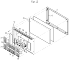
FIG. 2 is an exploded perspective view of the panel type display device according to the first exemplary embodiment of the present invention; and -
FIG. 3 is a sectional view of a panel type display device according to a second exemplary embodiment of the present invention. - Hereinafter, exemplary embodiments of the present invention will be described with reference to the accompanying drawings.
-
FIGS. 1 and2 illustrate a panel type display device according to a first embodiment of the present invention. The display device includes acase 10, adisplay panel 20 mounted at an inner front of thecase 10, and a plurality ofcircuit boards case 10. - The
case 10 includes afront case 11 coupled to thedisplay panel 20 at a front thereof and having anopening 13 formed at a screen portion, and arear case 12 of which an edge portion is coupled to thefront case 11 at a rear of thedisplay panel 20. - The
display panel 20 may be an LCD or a PDP. Thecircuit substrates display panel 20 through a flexible wiring part (not shown). A plurality of electronic components are mounted on thecircuit substrates display panel 20, a control circuit, a tuning circuit, a power circuit and the like. - As illustrated in
FIG. 2 , circuitboard mounting parts circuit boards rear case 12. Each of the circuitboard mounting parts rear case 12 such that thecircuit boards board mounting parts board mounting parts - As illustrated in
FIG. 1 , a plurality ofair inlets 61 through which air for cooling thedisplay panel 20 can flow in an interior of thecase 10 are formed at a lower portion of therear case 12, and a plurality ofair outlets 62 through which air in the interior of thecase 10 can be exhausted are formed at an upper portion of therear case 12. Further, as illustrated inFIG. 2 , a plurality ofair flow holes board mounting parts covers board mounting parts - As illustrated in
FIG. 1 , such components independently constitute a firstcooling fluid path 60 for cooling thedisplay panel 20 and secondcooling fluid paths 70 for respectively cooling thecircuit boards cooling fluid path 60 is formed by a space between a rear surface of thedisplay panel 20 and an inner surface of therear case 12, and the secondcooling fluid paths 70 are respectively formed by internal spaces of the circuitboard mounting parts rear case 12. Thus, the first and secondcooling fluid paths - Therefore, the
display panel 20 is cooled by air flowing along the firstcooling fluid path 60. Air flowing in through theair inlets 61 cools thedisplay panel 20 while rising along the firstcooling fluid path 60, and is then exhausted through theupper air outlets 62. Further, each of thecircuit boards cooling fluid path 70 through theair flow holes covers cooling fluid paths display panel 20 and thecircuit boards cooling fluid paths - In such a cooling structure, heat produced from the
circuit boards cooling fluid paths 70 without influencing thedisplay panel 20, and heat produced from the display panel can also be discharged through the firstcooling fluid path 60 without influencing thecircuit boards display panel 20 and thecircuit boards case 10 can be minimized. As an experimental result, such a cooling structure enabled a temperature of a front portion of the display panel to be dropped by about 5 to 7 °C as compared with a cooling structure of the conventional display device. - In
FIG. 2 , the circuitboard mounting parts rear case 12. However, the present invention is not limited thereto but may be implemented in such a manner that circuit boards are mounted to protrude from an outer surface of a rear case, and respectively covered with covers. -
FIG. 3 is a sectional view of a panel type display device according to a second exemplary embodiment of the present invention. In the second embodiment, apartition plate 500 for partitioning a cooling fluid path is mounted on an inner surface of arear case 120. Thus, in the state in whichcircuit boards 32 are mounted on an inner surface of thepartition plate 500, thepartition plate 500 can be mounted on the inner surface of therear case 120. That is, a circuit board mounting part is replaced by thepartition plate 500. Further, a plurality ofair flow holes rear case 120. A firstcooling fluid path 60 and air inlets andoutlets rear case 120 are identical with those of the first embodiment. That is, the first and secondcooling fluid paths 60 and 700 are separated from each other by thepartition plate 500 mounted on the inner surface of therear case 120 in the second embodiment. - As described above, in a panel type display device consistent with the present invention, first and second cooling fluid paths for respectively cooling a display panel and circuit boards are separated from each other, thereby preventing a phenomenon in which the circuit boards are heated by the heat of the display panel or the display panel is heated by the heat of the circuit boards. Accordingly, there is an advantage in that the cooling efficiency for the display panel and the circuit boards is enhanced, so that temperature increase in the interior of a case and the display panel can be minimized.
- Although exemplary embodiments of the present invention have been described for illustrative purposes, those skilled in the art will appreciate that various modifications, additions and substitutions are possible, without departing from the scope of the invention as disclosed in the accompanying claims.
Claims (10)
- A panel display device comprising:a case (10);a display panel (20) mounted in an interior of the case;at least one circuit board (32, 33) which controls the display panel;a first cooling fluid path (60) which cools the display panel; anda second cooling fluid path (70) which cools the circuit board, characterized in thatthe first and second cooling fluid paths are separated from each other by the case, such that a phenomenon in which the at least one circuit board is heated by the heat of the display panel or in which the display panel is heated by the heat of the at least one circuit board is prevented.
- The panel display device as claimed in claim 1, wherein the case includes front and rear cases (11, 12) coupled to each other, and the rear case includes a circuit board mounting part (41, 42, 43) provided on an outer surface of the rear case and a circuit board of the at least one circuit boards is mounted in the circuit board mounting part.
- The panel display device as claimed in claim 2, wherein the circuit board mounting part (41, 42, 43) has an open rear while being recessed from an outer surface of the rear case such that an internal space is formed in which the circuit board is mounted, and a cover (51, 52, 53) for covering the circuit board mounting part, on which a plurality of air flow holes (71, 72) are formed, is mounted on the circuit board mounting part.
- The panel display device as claimed in claim 3, wherein the first cooling fluid path includes a space between a rear surface of the display panel and an inner surface of the rear case, and the second cooling fluid path includes the internal space of the circuit board mounting part.
- The panel display device as claimed in claim 4, wherein air inlets (61) for air flowing in the first cooling fluid path are formed at a lower portion of the rear case, and air outlets (62) for air exhausting from the first cooling fluid path are formed at an upper portion of the rear case.
- The panel display device as claimed in claim 2, wherein a cover (51, 52, 53) for covering the circuit board mounting part, on which a plurality of air flow holes (71,7 2) are formed, is mounted on an outer rear surface of the rear case, the first cooling fluid path includes a space between a rear surface of the display panel and an inner surface of the rear case, and the second cooling fluid path includes a space confined by the circuit board mounting part and the cover.
- The panel display device as claimed in claim 1, wherein the case includes a circuit board mounting part (41, 42, 43) provided on a rear surface of the case and partitioned from a space in which the display panel is mounted and a circuit board of the at least one circuit boards is received in the circuit board mounting part, the first cooling fluid path includes a space between a rear surface of the display panel and an inner surface of the case, and the second cooling fluid path includes an internal space of the circuit board mounting part.
- A panel display device comprising:a case (11, 20);a partition plate (500) for dividing an interior of the case into a first and second cooling fluid path (60, 700);a display panel (20) mounted between the partition plate and a front surface of the case to be cooled by air flowing in the first cooling fluid path; andat least one circuit board (32) mounted between the partition plate and a rear surface of the case to be cooled by air flowing in the second cooling fluid path, characterized in thatsaid partition plate divides the interior of the case in a first space and a second space and that the case is formed with first inlets and first outlets leading in and out of said first space, respectively, and with second inlets and outlets leading in and out of the second space, respectively; and
the partition plate is such that a phenomenon in which the at least one circuit board is heated by the heat of the display panel or in which the display panel is heated by the heat of the at
least one circuit board is prevented. - The panel display device as claimed in claim 8, wherein air inlets and outlets (61, 62) are formed at lower and upper portions of the case, respectively, for allowing air to flow into the first cooling fluid path.
- The panel display device as claimed in claim 8, wherein a plurality of air flow holes (710, 720) through which air flows are formed on the rear surface of the case for allowing air to flow into the second cooling fluid path.
Applications Claiming Priority (1)
| Application Number | Priority Date | Filing Date | Title |
|---|---|---|---|
| KR1020070002081A KR101273592B1 (en) | 2007-01-08 | 2007-01-08 | Panel type display device |
Publications (3)
| Publication Number | Publication Date |
|---|---|
| EP1942367A2 EP1942367A2 (en) | 2008-07-09 |
| EP1942367A3 EP1942367A3 (en) | 2010-04-28 |
| EP1942367B1 true EP1942367B1 (en) | 2019-03-20 |
Family
ID=39203321
Family Applications (1)
| Application Number | Title | Priority Date | Filing Date |
|---|---|---|---|
| EP07118363.6A Ceased EP1942367B1 (en) | 2007-01-08 | 2007-10-12 | Panel type display device |
Country Status (4)
| Country | Link |
|---|---|
| US (2) | US7667964B2 (en) |
| EP (1) | EP1942367B1 (en) |
| KR (1) | KR101273592B1 (en) |
| CN (1) | CN101221300A (en) |
Families Citing this family (97)
| Publication number | Priority date | Publication date | Assignee | Title |
|---|---|---|---|---|
| KR101435801B1 (en) * | 2007-08-30 | 2014-08-29 | 엘지전자 주식회사 | Display device |
| KR101456975B1 (en) * | 2007-09-27 | 2014-10-31 | 삼성전자 주식회사 | Cooling unit and display device having the same |
| US12185512B2 (en) | 2007-11-16 | 2024-12-31 | Manufacturing Resources International, Inc. | Electronic display assembly with thermal management |
| US8854595B2 (en) | 2008-03-03 | 2014-10-07 | Manufacturing Resources International, Inc. | Constricted convection cooling system for an electronic display |
| JP5201964B2 (en) * | 2007-12-03 | 2013-06-05 | 三洋電機株式会社 | Image display device |
| JP2009175230A (en) * | 2008-01-22 | 2009-08-06 | Sharp Corp | Display device |
| KR100893619B1 (en) * | 2008-02-18 | 2009-04-20 | 삼성모바일디스플레이주식회사 | Electronic device with organic light emitting display |
| US8274622B2 (en) | 2008-03-03 | 2012-09-25 | Manufacturing Resources International, Inc. | System for using constricted convection with closed loop plenum as the convection plate |
| US9173325B2 (en) | 2008-03-26 | 2015-10-27 | Manufacturing Resources International, Inc. | Heat exchanger for back to back electronic displays |
| US8497972B2 (en) | 2009-11-13 | 2013-07-30 | Manufacturing Resources International, Inc. | Thermal plate with optional cooling loop in electronic display |
| US8654302B2 (en) | 2008-03-03 | 2014-02-18 | Manufacturing Resources International, Inc. | Heat exchanger for an electronic display |
| US8773633B2 (en) | 2008-03-03 | 2014-07-08 | Manufacturing Resources International, Inc. | Expanded heat sink for electronic displays |
| US8693185B2 (en) | 2008-03-26 | 2014-04-08 | Manufacturing Resources International, Inc. | System and method for maintaining a consistent temperature gradient across an electronic display |
| KR101387932B1 (en) * | 2008-05-07 | 2014-04-23 | 삼성전자주식회사 | Display unit and vending maching having the same |
| CN102105832A (en) * | 2008-07-28 | 2011-06-22 | Nec显示器解决方案株式会社 | Display device |
| CN102113331A (en) * | 2008-07-29 | 2011-06-29 | 汤姆森特许公司 | Display characterization with filtration |
| JP2010039408A (en) * | 2008-08-08 | 2010-02-18 | Panasonic Corp | Image display device |
| JP5241416B2 (en) * | 2008-09-30 | 2013-07-17 | 三洋電機株式会社 | Image display device |
| JP5241414B2 (en) * | 2008-09-30 | 2013-07-17 | 三洋電機株式会社 | Image display device |
| TWI380075B (en) * | 2008-10-17 | 2012-12-21 | Au Optronics Corp | Liquid crystal display and fabricating method thereof |
| US8749749B2 (en) | 2008-12-18 | 2014-06-10 | Manufacturing Resources International, Inc. | System for cooling an electronic image assembly with manifolds and ambient gas |
| US10827656B2 (en) | 2008-12-18 | 2020-11-03 | Manufacturing Resources International, Inc. | System for cooling an electronic image assembly with circulating gas and ambient gas |
| KR100969937B1 (en) * | 2008-12-29 | 2010-07-14 | 주식회사 케이에스비 | Digital display board having a fast cooling module for lcd and led pannel |
| KR100952120B1 (en) * | 2008-12-29 | 2010-04-09 | 주식회사 케이에스비 | Fast cooling module for lcd and led pannel of digital display board |
| TWM361858U (en) * | 2009-01-05 | 2009-07-21 | Coretronic Display Solution Corp | Flat panel display |
| JP5374166B2 (en) * | 2009-01-09 | 2013-12-25 | キヤノン株式会社 | Thin panel display |
| JP5451140B2 (en) * | 2009-03-31 | 2014-03-26 | パナソニック液晶ディスプレイ株式会社 | Display device |
| KR101670985B1 (en) * | 2010-01-07 | 2016-10-31 | 삼성전자 주식회사 | Display Apparatus |
| EP2567283B1 (en) * | 2010-05-04 | 2019-10-16 | Manufacturing Resources International, Inc. | System for cooling an electronic image assembly |
| JP5061225B2 (en) * | 2010-08-19 | 2012-10-31 | シャープ株式会社 | Display device |
| KR20120066766A (en) * | 2010-12-15 | 2012-06-25 | 삼성전자주식회사 | Liquid crystal display and driving method threrof |
| KR101042781B1 (en) * | 2011-02-01 | 2011-06-20 | 임영기 | LED billboard assembly with support |
| KR101737391B1 (en) | 2011-02-01 | 2017-05-30 | 삼성전자주식회사 | Outdoor display apparatus |
| JP5845795B2 (en) | 2011-10-12 | 2016-01-20 | 船井電機株式会社 | Display device |
| JPWO2012114701A1 (en) * | 2011-02-22 | 2014-07-07 | パナソニック株式会社 | Display device manufacturing method |
| JP5836626B2 (en) * | 2011-04-18 | 2015-12-24 | 三菱電機株式会社 | Thin display device |
| WO2012157547A1 (en) * | 2011-05-18 | 2012-11-22 | シャープ株式会社 | Display device |
| US8625047B2 (en) * | 2011-05-31 | 2014-01-07 | Microsoft Corporation | Fluid ingress resistant interactive display device |
| US20130114213A1 (en) * | 2011-11-09 | 2013-05-09 | Silicon Intergrated Systems Corp. | Electronic device |
| US20130128348A1 (en) * | 2011-11-18 | 2013-05-23 | Shenzhen China Star Optoelectronics Technology Co., Ltd. | Flat Panel Display Device, Stereoscopic Display Device, Plasma Display Device |
| WO2014030584A1 (en) * | 2012-08-21 | 2014-02-27 | シャープ株式会社 | Illumination device, display device, and tv reception device |
| EP2701475A1 (en) * | 2012-08-22 | 2014-02-26 | Ruf Telematik AG | Housing for holding a flat screen |
| KR101868077B1 (en) * | 2012-10-16 | 2018-06-18 | 매뉴팩처링 리소시스 인터내셔널 인코포레이티드 | Back pan cooling assembly for electric display |
| US9648790B2 (en) | 2013-03-15 | 2017-05-09 | Manufacturing Resources International, Inc. | Heat exchanger assembly for an electronic display |
| US10524384B2 (en) | 2013-03-15 | 2019-12-31 | Manufacturing Resources International, Inc. | Cooling assembly for an electronic display |
| JPWO2014155722A1 (en) * | 2013-03-29 | 2017-02-16 | 株式会社東芝 | Display device |
| CA2917868A1 (en) | 2013-07-08 | 2015-01-15 | Manufacturing Resources International, Inc. | Figure eight closed loop cooling system for electronic display |
| US20150131022A1 (en) * | 2013-11-13 | 2015-05-14 | Shenzhen China Star Optoelectronics Technology Co. Ltd. | Multiple display monitor |
| KR102180911B1 (en) * | 2013-12-12 | 2020-11-19 | 엘지디스플레이 주식회사 | Display apparatus |
| CN103731978A (en) * | 2013-12-31 | 2014-04-16 | 深圳市华星光电技术有限公司 | Printed circuit board and display device utilizing same |
| ES2745563T3 (en) | 2014-03-11 | 2020-03-02 | Mri Inc | Hybrid back cover and mounting bracket for an electronic display |
| CA2947524C (en) | 2014-04-30 | 2018-04-03 | Manufacturing Resources International, Inc. | Back to back electronic display assembly |
| EP3040766B1 (en) * | 2015-01-05 | 2018-01-31 | Samsung Electronics Co., Ltd. | Display device |
| US20160227156A1 (en) * | 2015-02-02 | 2016-08-04 | Hisense Hiview Tech Co., Ltd. | Modular television system |
| US9723765B2 (en) | 2015-02-17 | 2017-08-01 | Manufacturing Resources International, Inc. | Perimeter ventilation system for electronic display |
| US9943017B2 (en) * | 2015-04-30 | 2018-04-10 | Premier Mounts | Enclosure device for displays |
| JP2017015911A (en) * | 2015-06-30 | 2017-01-19 | キヤノン株式会社 | Display device |
| AU2016231519A1 (en) * | 2015-09-22 | 2017-04-06 | Coates Technology Labs Pty Limited | Display housing for a digital display screen |
| EP3163362B1 (en) * | 2015-10-27 | 2019-03-13 | LG Electronics Inc. | Display device |
| EP3423886B1 (en) | 2016-03-04 | 2022-02-16 | Manufacturing Resources International, Inc. | Cooling system for double sided display assembly |
| TWM523876U (en) * | 2016-04-08 | 2016-06-11 | 揚昇照明股份有限公司 | Display device |
| KR102236771B1 (en) | 2016-12-02 | 2021-04-06 | 삼성전자주식회사 | Outdoor display apparatus |
| JP2018152524A (en) * | 2017-03-15 | 2018-09-27 | 東芝メモリ株式会社 | Electronics |
| WO2018199452A1 (en) * | 2017-04-23 | 2018-11-01 | Lg Electronics Inc. | Display device |
| US10398066B2 (en) | 2017-04-27 | 2019-08-27 | Manufacturing Resources International, Inc. | System and method for preventing display bowing |
| US10485113B2 (en) | 2017-04-27 | 2019-11-19 | Manufacturing Resources International, Inc. | Field serviceable and replaceable display |
| KR101961638B1 (en) * | 2017-08-07 | 2019-03-25 | 주식회사 이베스트 | Device for sterilizing microphone |
| KR102408902B1 (en) * | 2017-08-16 | 2022-06-15 | 엘지디스플레이 주식회사 | Display Unit |
| US10559965B2 (en) | 2017-09-21 | 2020-02-11 | Manufacturing Resources International, Inc. | Display assembly having multiple charging ports |
| TWM561221U (en) * | 2017-12-12 | 2018-06-01 | 緯創資通股份有限公司 | Display assembly with heat disspation structure |
| US10602626B2 (en) | 2018-07-30 | 2020-03-24 | Manufacturing Resources International, Inc. | Housing assembly for an integrated display unit |
| KR102646114B1 (en) * | 2018-11-09 | 2024-03-12 | 삼성전자주식회사 | Display apparatus |
| US11096317B2 (en) | 2019-02-26 | 2021-08-17 | Manufacturing Resources International, Inc. | Display assembly with loopback cooling |
| US10795413B1 (en) | 2019-04-03 | 2020-10-06 | Manufacturing Resources International, Inc. | Electronic display assembly with a channel for ambient air in an access panel |
| EP3783422B1 (en) * | 2019-08-16 | 2024-02-28 | Bme Messgeräte Entwicklung Kg | An optical system comprising a symmetric cooling arrangement for cooling an optical device |
| KR102611291B1 (en) * | 2019-10-18 | 2023-12-08 | 엘지전자 주식회사 | display device |
| US11477923B2 (en) | 2020-10-02 | 2022-10-18 | Manufacturing Resources International, Inc. | Field customizable airflow system for a communications box |
| US11470749B2 (en) | 2020-10-23 | 2022-10-11 | Manufacturing Resources International, Inc. | Forced air cooling for display assemblies using centrifugal fans |
| US11778757B2 (en) | 2020-10-23 | 2023-10-03 | Manufacturing Resources International, Inc. | Display assemblies incorporating electric vehicle charging equipment |
| JP7555256B2 (en) * | 2020-12-10 | 2024-09-24 | シャープ株式会社 | Electronic device and display device |
| JP7606403B2 (en) * | 2021-04-23 | 2024-12-25 | シャープ株式会社 | Display device |
| TWI768854B (en) * | 2021-04-28 | 2022-06-21 | 緯創資通股份有限公司 | Heat dissipating mechanism and display apparatus thereof |
| JP7681444B2 (en) * | 2021-06-22 | 2025-05-22 | 株式会社日立製作所 | electronic equipment |
| US12408312B2 (en) | 2021-07-28 | 2025-09-02 | Manufacturing Resources International, Inc. | Display assemblies with vents |
| US11966263B2 (en) | 2021-07-28 | 2024-04-23 | Manufacturing Resources International, Inc. | Display assemblies for providing compressive forces at electronic display layers |
| US11919393B2 (en) | 2021-08-23 | 2024-03-05 | Manufacturing Resources International, Inc. | Display assemblies inducing relatively turbulent flow and integrating electric vehicle charging equipment |
| US11762231B2 (en) | 2021-08-23 | 2023-09-19 | Manufacturing Resources International, Inc. | Display assemblies inducing turbulent flow |
| US11744054B2 (en) | 2021-08-23 | 2023-08-29 | Manufacturing Resources International, Inc. | Fan unit for providing improved airflow within display assemblies |
| US11968813B2 (en) | 2021-11-23 | 2024-04-23 | Manufacturing Resources International, Inc. | Display assembly with divided interior space |
| GB2614749B (en) * | 2022-01-18 | 2024-10-09 | Amscreen Group Ltd | Cooling of electronic displays |
| US12010813B2 (en) | 2022-07-22 | 2024-06-11 | Manufacturing Resources International, Inc. | Self-contained electronic display assembly, mounting structure and methods for the same |
| US12072561B2 (en) | 2022-07-22 | 2024-08-27 | Manufacturing Resources International, Inc. | Self-contained electronic display assembly, mounting structure and methods for the same |
| US12035486B1 (en) | 2022-07-25 | 2024-07-09 | Manufacturing Resources International, Inc. | Electronic display assembly with fabric panel communications box |
| KR20240026397A (en) * | 2022-08-19 | 2024-02-28 | 삼성디스플레이 주식회사 | Electronic apparatus |
| TWI865044B (en) * | 2023-09-14 | 2024-12-01 | 達擎股份有限公司 | Display device |
| US12598727B2 (en) | 2024-01-09 | 2026-04-07 | Manufacturing Resources International, Inc. | Double sided display assembly with bi-directional flow through a common, partitioned heat exchanger |
| KR102802082B1 (en) * | 2024-11-19 | 2025-05-02 | 하나시스 주식회사 | Display device and POS device that utilize them |
Family Cites Families (15)
| Publication number | Priority date | Publication date | Assignee | Title |
|---|---|---|---|---|
| US4980848A (en) * | 1988-10-31 | 1990-12-25 | Zenith Data Systems Corporation | Heat-exchange panel for portable computer |
| JP3234740B2 (en) * | 1994-06-09 | 2001-12-04 | キヤノン株式会社 | Image display device |
| US5971566A (en) * | 1996-07-23 | 1999-10-26 | Matsushita Electric Industrial Co., Ltd. | Plasma display device and its manufacturing method |
| TW445386B (en) * | 1998-03-16 | 2001-07-11 | Hitachi Ltd | Thin-type display |
| TW393666B (en) * | 1998-06-15 | 2000-06-11 | Acer Display Tech Inc | A plasma display device having a heated airflow guiding groove |
| JP2001264754A (en) | 2000-03-15 | 2001-09-26 | Nec Corp | Liquid crystal display device and light source device used therefor |
| JP2002006754A (en) * | 2000-06-19 | 2002-01-11 | Pioneer Electronic Corp | Radiation structure of plasma display panel device |
| JP2003075858A (en) * | 2001-08-31 | 2003-03-12 | Matsushita Electric Works Ltd | Heat radiation structure of wall-buried type liquid crystal panel unit |
| KR100445033B1 (en) * | 2002-08-26 | 2004-08-18 | 삼성에스디아이 주식회사 | A case for covering electronic parts and a displaying apparatus having it |
| KR100522695B1 (en) * | 2003-09-01 | 2005-10-19 | 삼성에스디아이 주식회사 | Display apparatus |
| TWI268526B (en) * | 2003-12-05 | 2006-12-11 | Au Optronics Corp | Plasma display |
| KR100637439B1 (en) * | 2004-05-19 | 2006-10-20 | 삼성에스디아이 주식회사 | Plasma display device |
| JP2006162641A (en) | 2004-12-02 | 2006-06-22 | Matsushita Electric Ind Co Ltd | Plasma display device |
| TWI266125B (en) * | 2005-07-15 | 2006-11-11 | Au Optronics Corp | Direct type backlight module |
| JP2007110200A (en) * | 2005-10-11 | 2007-04-26 | Orion Denki Kk | Video display with information recorder/reproducer |
-
2007
- 2007-01-08 KR KR1020070002081A patent/KR101273592B1/en active Active
- 2007-10-12 EP EP07118363.6A patent/EP1942367B1/en not_active Ceased
- 2007-10-15 US US11/872,057 patent/US7667964B2/en not_active Ceased
- 2007-10-29 CN CNA2007101654493A patent/CN101221300A/en active Pending
-
2012
- 2012-02-23 US US13/403,559 patent/USRE45117E1/en active Active
Non-Patent Citations (1)
| Title |
|---|
| None * |
Also Published As
| Publication number | Publication date |
|---|---|
| EP1942367A3 (en) | 2010-04-28 |
| CN101221300A (en) | 2008-07-16 |
| USRE45117E1 (en) | 2014-09-09 |
| KR20080065108A (en) | 2008-07-11 |
| KR101273592B1 (en) | 2013-06-11 |
| US20080165496A1 (en) | 2008-07-10 |
| US7667964B2 (en) | 2010-02-23 |
| EP1942367A2 (en) | 2008-07-09 |
Similar Documents
| Publication | Publication Date | Title |
|---|---|---|
| US7667964B2 (en) | Panel type display device | |
| US7667968B2 (en) | Air-cooling system configuration for touch screen | |
| EP3280135A1 (en) | Display device | |
| US7206039B2 (en) | Flat display apparatus having partitioned housing | |
| JP2010081280A (en) | Video display apparatus | |
| KR100759553B1 (en) | Plasma display module | |
| JP4294423B2 (en) | Liquid crystal display | |
| KR20210009716A (en) | Display device | |
| JP2011180476A (en) | Image display device | |
| JP2009276759A (en) | Image display apparatus | |
| JP2008040424A (en) | Air path configuration and cooling structure of thin image display device | |
| JP2014059502A (en) | Display device | |
| JP4309706B2 (en) | Flat panel display | |
| AU2005220272B2 (en) | Electronic equipment | |
| JP4276223B2 (en) | Plasma display device | |
| KR100669701B1 (en) | Plasma display device | |
| KR100592263B1 (en) | Plasma display device | |
| KR100637138B1 (en) | Plasma display device | |
| JP2010139840A (en) | Image display device and attaching metal fitting | |
| WO2019163555A1 (en) | Image display device | |
| KR100683690B1 (en) | Plasma display module | |
| JP2000112390A (en) | Display device | |
| KR100637225B1 (en) | Plasma display | |
| KR100615296B1 (en) | Plasma display device | |
| KR100717787B1 (en) | Plasma display device |
Legal Events
| Date | Code | Title | Description |
|---|---|---|---|
| PUAI | Public reference made under article 153(3) epc to a published international application that has entered the european phase |
Free format text: ORIGINAL CODE: 0009012 |
|
| AK | Designated contracting states |
Kind code of ref document: A2 Designated state(s): AT BE BG CH CY CZ DE DK EE ES FI FR GB GR HU IE IS IT LI LT LU LV MC MT NL PL PT RO SE SI SK TR |
|
| AX | Request for extension of the european patent |
Extension state: AL BA HR MK RS |
|
| PUAL | Search report despatched |
Free format text: ORIGINAL CODE: 0009013 |
|
| AK | Designated contracting states |
Kind code of ref document: A3 Designated state(s): AT BE BG CH CY CZ DE DK EE ES FI FR GB GR HU IE IS IT LI LT LU LV MC MT NL PL PT RO SE SI SK TR |
|
| AX | Request for extension of the european patent |
Extension state: AL BA HR MK RS |
|
| 17P | Request for examination filed |
Effective date: 20100922 |
|
| 17Q | First examination report despatched |
Effective date: 20101028 |
|
| AKX | Designation fees paid |
Designated state(s): DE GB NL |
|
| RAP1 | Party data changed (applicant data changed or rights of an application transferred) |
Owner name: SAMSUNG ELECTRONICS CO., LTD. |
|
| GRAP | Despatch of communication of intention to grant a patent |
Free format text: ORIGINAL CODE: EPIDOSNIGR1 |
|
| INTG | Intention to grant announced |
Effective date: 20181012 |
|
| GRAS | Grant fee paid |
Free format text: ORIGINAL CODE: EPIDOSNIGR3 |
|
| GRAA | (expected) grant |
Free format text: ORIGINAL CODE: 0009210 |
|
| AK | Designated contracting states |
Kind code of ref document: B1 Designated state(s): DE GB NL |
|
| REG | Reference to a national code |
Ref country code: GB Ref legal event code: FG4D |
|
| REG | Reference to a national code |
Ref country code: DE Ref legal event code: R096 Ref document number: 602007057880 Country of ref document: DE |
|
| REG | Reference to a national code |
Ref country code: NL Ref legal event code: FP |
|
| REG | Reference to a national code |
Ref country code: DE Ref legal event code: R097 Ref document number: 602007057880 Country of ref document: DE |
|
| PLBE | No opposition filed within time limit |
Free format text: ORIGINAL CODE: 0009261 |
|
| STAA | Information on the status of an ep patent application or granted ep patent |
Free format text: STATUS: NO OPPOSITION FILED WITHIN TIME LIMIT |
|
| 26N | No opposition filed |
Effective date: 20200102 |
|
| REG | Reference to a national code |
Ref country code: DE Ref legal event code: R119 Ref document number: 602007057880 Country of ref document: DE |
|
| PG25 | Lapsed in a contracting state [announced via postgrant information from national office to epo] |
Ref country code: DE Free format text: LAPSE BECAUSE OF NON-PAYMENT OF DUE FEES Effective date: 20200501 |
|
| GBPC | Gb: european patent ceased through non-payment of renewal fee |
Effective date: 20191012 |
|
| PG25 | Lapsed in a contracting state [announced via postgrant information from national office to epo] |
Ref country code: GB Free format text: LAPSE BECAUSE OF NON-PAYMENT OF DUE FEES Effective date: 20191012 |
|
| PGFP | Annual fee paid to national office [announced via postgrant information from national office to epo] |
Ref country code: NL Payment date: 20200928 Year of fee payment: 14 |
|
| REG | Reference to a national code |
Ref country code: NL Ref legal event code: MM Effective date: 20211101 |
|
| PG25 | Lapsed in a contracting state [announced via postgrant information from national office to epo] |
Ref country code: NL Free format text: LAPSE BECAUSE OF NON-PAYMENT OF DUE FEES Effective date: 20211101 |