EP1939948A2 - Method and apparatus for breaking semiconductor substrate, method for breaking solar cell and method for fabrication of solar cell module - Google Patents
Method and apparatus for breaking semiconductor substrate, method for breaking solar cell and method for fabrication of solar cell module Download PDFInfo
- Publication number
- EP1939948A2 EP1939948A2 EP20070025018 EP07025018A EP1939948A2 EP 1939948 A2 EP1939948 A2 EP 1939948A2 EP 20070025018 EP20070025018 EP 20070025018 EP 07025018 A EP07025018 A EP 07025018A EP 1939948 A2 EP1939948 A2 EP 1939948A2
- Authority
- EP
- European Patent Office
- Prior art keywords
- semiconductor substrate
- breaking
- predetermined area
- solar cell
- split groove
- Prior art date
- Legal status (The legal status is an assumption and is not a legal conclusion. Google has not performed a legal analysis and makes no representation as to the accuracy of the status listed.)
- Granted
Links
Images

Classifications
-
- H—ELECTRICITY
- H10—SEMICONDUCTOR DEVICES; ELECTRIC SOLID-STATE DEVICES NOT OTHERWISE PROVIDED FOR
- H10F—INORGANIC SEMICONDUCTOR DEVICES SENSITIVE TO INFRARED RADIATION, LIGHT, ELECTROMAGNETIC RADIATION OF SHORTER WAVELENGTH OR CORPUSCULAR RADIATION
- H10F71/00—Manufacture or treatment of devices covered by this subclass
- H10F71/136—Singulating, e.g. dicing
-
- H—ELECTRICITY
- H10—SEMICONDUCTOR DEVICES; ELECTRIC SOLID-STATE DEVICES NOT OTHERWISE PROVIDED FOR
- H10F—INORGANIC SEMICONDUCTOR DEVICES SENSITIVE TO INFRARED RADIATION, LIGHT, ELECTROMAGNETIC RADIATION OF SHORTER WAVELENGTH OR CORPUSCULAR RADIATION
- H10F71/00—Manufacture or treatment of devices covered by this subclass
-
- B—PERFORMING OPERATIONS; TRANSPORTING
- B26—HAND CUTTING TOOLS; CUTTING; SEVERING
- B26F—PERFORATING; PUNCHING; CUTTING-OUT; STAMPING-OUT; SEVERING BY MEANS OTHER THAN CUTTING
- B26F3/00—Severing by means other than cutting; Apparatus therefor
- B26F3/002—Precutting and tensioning or breaking
-
- H—ELECTRICITY
- H10—SEMICONDUCTOR DEVICES; ELECTRIC SOLID-STATE DEVICES NOT OTHERWISE PROVIDED FOR
- H10P—GENERIC PROCESSES OR APPARATUS FOR THE MANUFACTURE OR TREATMENT OF DEVICES COVERED BY CLASS H10
- H10P72/00—Handling or holding of wafers, substrates or devices during manufacture or treatment thereof
- H10P72/04—Apparatus for manufacture or treatment
- H10P72/0428—Apparatus for mechanical treatment or grinding or cutting
-
- Y—GENERAL TAGGING OF NEW TECHNOLOGICAL DEVELOPMENTS; GENERAL TAGGING OF CROSS-SECTIONAL TECHNOLOGIES SPANNING OVER SEVERAL SECTIONS OF THE IPC; TECHNICAL SUBJECTS COVERED BY FORMER USPC CROSS-REFERENCE ART COLLECTIONS [XRACs] AND DIGESTS
- Y10—TECHNICAL SUBJECTS COVERED BY FORMER USPC
- Y10T—TECHNICAL SUBJECTS COVERED BY FORMER US CLASSIFICATION
- Y10T225/00—Severing by tearing or breaking
- Y10T225/30—Breaking or tearing apparatus
- Y10T225/307—Combined with preliminary weakener or with nonbreaking cutter
- Y10T225/321—Preliminary weakener
- Y10T225/325—With means to apply moment of force to weakened work
-
- Y—GENERAL TAGGING OF NEW TECHNOLOGICAL DEVELOPMENTS; GENERAL TAGGING OF CROSS-SECTIONAL TECHNOLOGIES SPANNING OVER SEVERAL SECTIONS OF THE IPC; TECHNICAL SUBJECTS COVERED BY FORMER USPC CROSS-REFERENCE ART COLLECTIONS [XRACs] AND DIGESTS
- Y10—TECHNICAL SUBJECTS COVERED BY FORMER USPC
- Y10T—TECHNICAL SUBJECTS COVERED BY FORMER US CLASSIFICATION
- Y10T225/00—Severing by tearing or breaking
- Y10T225/30—Breaking or tearing apparatus
- Y10T225/371—Movable breaking tool
Definitions
- the present invention relates to a method and apparatus for breaking a semiconductor substrate, made by forming a photovoltaic element or other element structure on a silicon wafer or the like, along a predetermined region over which a split groove is formed, a method for breaking a solar cell utilizing the above method and apparatus, and a method for fabrication of a solar cell module.
- the method for breaking a semiconductor substrate is a method in which a semiconductor substrate is broken along a predetermined area over which a split groove is formed, and is characterized as including the steps of holding the semiconductor substrate in position and pressing a portion of the semiconductor substrate outside the predetermined area to break the semiconductor substrate along the split groove, wherein the predetermined area has at least a neighboring pair of sides intersecting at an angle of less than 180 degrees and, when the semiconductor substrate is broken, one of the sides is pressed ahead of the other side.
- the predetermined area of the semiconductor substrate has at least a neighboring pair of sides intersecting at an angle of less than 180 degrees.
- Each of the neighboring, pair of sides may not be necessarily linear and may include a curve. They just need to intersect at an angle of less than 180 degrees.
- the reason why the intersecting angle is specified in the present invention as being less than 180 degrees is because a stress tends to concentrate at an edge portion where the two sides intersect at such an angle.
- one of such pair of sides is compressed ahead of the other in breaking the semiconductor substrate. This suppresses stress concentration at an edge portion defined by the pair of sides and accordingly prevents the occurrence of cracking or the like.
- simultaneous application of a pressing force on the pair of sides causes stress concentration at the edge portion defined by the pair of sides and increases the occurrence of cracking or the like at such a portion.
- one side is compressed ahead of the other side. Accordingly, a stress is first exerted on the one side in its entirety so that breaking starts to occur along a scribed portion running over the one side. Subsequently, the stress is exerted on the other side in its entirety so that breaking starts to occur in the other side.
- the practice of such multi-stage breaking suppresses stress concentration at the edge portion where the one side meets with the other side and thus prevents the occurrence of cracking or the like.
- the portion of the semiconductor substrate inside the predetermined area is placed on a table. Thereafter, a breaking blade, located above the semiconductor substrate on the table, is moved downward to compress the portion of the semiconductor substrate outside the predetermined area so that the semiconductor substrate is broken along the split groove.
- the apparatus of the present invention for breaking a semiconductor substrate is an apparatus which utilizes the aforementioned method of the present invention to break the semiconductor substrate along the predetermined area over which the split groove is formed.
- the apparatus includes a table for placement of the portion of the semiconductor substrate inside the predetermined area and a breaking blade operable to move downward from a position above the semiconductor substrate placed on the table and compress the portion of the semiconductor substrate outside the predetermined area so that the semiconductor substrate is broken along the split groove.
- the predetermined area of the semiconductor substrate has at least a neighboring pair of sides intersecting at an angle of less than 180 degrees
- the breaking blade has a projection which, in breaking the semiconductor substrate, compresses a portion of the semiconductor substrate outside the one side so that the one side is compressed ahead of the other side.
- the breaking blade has a projection which, when the semiconductor substrate is broken, compresses a portion of the semiconductor substrate outside the one side so that the one side is compressed ahead of the other side, as described above.
- the projection of the breaking blade By the action of the projection of the breaking blade, the one side is compressed ahead of the other side. This suppresses stress concentration at the edge portion where the one side meets the other side and prevents the occurrence of cracking or the like, as similar to the breaking method of the present invention.
- the breaking apparatus of the present invention further includes a press member for pressing the portion of the semiconductor substrate inside the predetermined area against the table from above so that the semiconductor substrate is held firmly in position when it is broken.
- the provision of the press member makes it easy to firmly hold the semiconductor substrate placed on the table in position.
- a shape of the predetermined area defined by the split groove formed on the semiconductor substrate may be ring-like or linear such as a straight or curved line.
- a shape of the predetermined region defined by the split groove is ring-like.
- the breaking blade used is generally ring-shaped. In the case where the ring-shaped breaking blade is used, it preferably has a hole of a size that allows the table to pass therethrough.
- an inner end face of the projection preferably has a taper that extends downwardly and outwardly.
- the provision of such a taper allows smooth bending of the portion of the semiconductor substrate outside the predetermined area, leading to breaking thereof along the split groove.
- a portion of the breaking blade that lacks the projection and exerts a pressure on the portion of the semiconductor substrate outside the predetermined area preferably has a taper which extends downwardly outwardly. The provision of such a taper allows smooth bending of the semiconductor substrate portion outside the predetermined area, leading to breaking thereof along the split groove.
- the height of the projection is not particularly specified, but is generally preferably in the range of 0.5 - 50 mm, more preferably in the range of 1 - 10 mm.
- the breaking blade because of provision of the projections, has portions lacking the projection and those having the projection and can thus compress the semiconductor substrate by at least two stages.
- the projections may have different heights.
- the breaking blade can compress the semiconductor substrate by three or more stages, leading to breaking thereof.
- the breaking method and apparatus of the present invention is useful in removing a peripheral portion of a semiconductor substrate in the fabrication of a solar cell or in dividing a large-area semiconductor substrate into individual small-area solar cells. Accordingly, a semiconductor substrate having solar cell element structures formed thereon can be illustrated as one form of the semiconductor substrate for use in the present invention.
- a semiconductor substrate is broken using the breaking method or apparatus of the present invention. Therefore, the occurrence of cracking in breaking the semiconductor substrate can be prevented. As a result, a solar cell module can be fabricated with a good yield rate.
- the present invention can prevent the occurrence of cracking or the like due to stress concentration at a portion of the semiconductor substrate that is caused when the semiconductor substrate is broken along the predetermined area over which the split groove is formed.
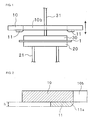
- Figure 1 is a side view which shows an embodiment of an apparatus for breaking a semiconductor substrate in accordance with the present invention.
- a semiconductor substrate 1 is placed on a table 20 and held in position by a press member 30 which is supported from above by a rod 31 and compresses the substrate against the table 20.
- the table 20 is supported from below by rods 21.
- the method by which the semiconductor substrate is held in position is not limited thereto.
- the breaking blade 10 is ring-shaped and has an interior central hole 10b which is sized to allow passage of the press member 30 and the table 20.
- a projection forming member 11 is attached to an inner portion of a lower face of the ring-shaped breaking blade 10. Although not shown, the breaking blade 10 is supported from above by rods for vertical movement.
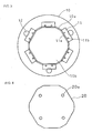
- Figure 2 is an enlarged sectional view which shows the breaking blade 10 and the projection forming member 11.
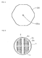
- Figure 3 is a plan view which shows a lower face of the breaking blade 10. As shown in Figures 2 and 3 , an inner end face of the projection forming member 11 has a taper 11a which extends downwardly and outwardly.
- the interior hole 10a of the breaking blade 10 has a generally dodecagonal shape.
- the projection forming member 11 is mounted to every other side and accordingly to six sides in total.
- An inner end surface of the breaking blade, where the projection forming members 11 are not mounted, has a taper 10a at its lower portion. This taper 10a is configured to extend downwardly and outwardly, as similar to the taper 11a of the projection forming member 11.
- the breaking blade 10 has circumferentially arranged three holes 12 for passage of rods which together support the breaking blade from above.
- the central hole 10b of the breaking blade 10 has a generally dodecagonal shape.
- the one side to which the projection forming member 11 is mounted and the adjacent side to which the projection forming member 11 is not mounted intersect at an angle of less than 180 degrees.
- the neighboring pair of sides are shown to intersect at an angle of about 160 degrees.
- the side to which the projection forming member 11 is not mounted appears somewhat rounded, its end portions meet the respective adjacent sides each contiguous with an inner end of the projection formingmember 11 at an angle of less than 180 degrees, as specified in the present invention.
- the height of the projection in the present invention can be suitably set up considering a rate of movement of the breaking blade and others. However, it is generally preferably in the range of 1 - 10 mm, as described above.
- Figure 4 is plan view which shows the table 20.
- the table is sized to pass through the hole 10b of the breaking blade 10 and has a shape analogous to that of the hole 10b.
- the respective shapes of the hole 10b of the breaking blade 10 and the table 20 nearly correspond to the shape of the predetermined area along which the split groove is formed in the semiconductor substrate.
- the table 20 has a central hole 20a for passage of the rods 21 shown in Figure 1 for supporting the table 20.
- Figure 5 is a plan view which shows the press member 30 shown in Figure 1 .
- the press member 30 is also sized to pass through the hole 10a of the breaking blade 10 and has a shape contiguous to that of the hole 10a.
- breaking blade 10, projection forming member 11 and table 20 are not particularly specified in material type, they are all made of stainless steel in this embodiment. Also, the material type of the press member shown in Figure 5 is not particularly specified. However, in this embodiment, it is formed of an engineering plastic or other plastic member.
- the respective material types of the rods for supporting the breaking blade 10, table 20 and press member 30 are not particularly specified. However, they are all made of stainless steel in this embodiment.
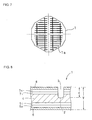
- FIG. 6 is a plan view which shows the semiconductor substrate 1 as it is used in a solar cell.
- the solar cell 1 has a current collecting electrode 1a and a ring-shaped predetermined area 2 extending along its outer periphery.
- Figure 8 is an enlarged sectional area which shows the predetermined area 2 in the solar cell 1 and its surroundings.
- a split groove 3 is formed over the predetermined area 2 in the solar cell 1.
- the split groove 3 can be formed, for example, by irradiating the solar cell with an energy beam such as a laser beam.
- useful lasers include a YAG laser, gas lasers such as a CO 2 laser, KrF laser, ArF laser and XeCl laser, and solid lasers such as an YVO4 laser.
- the depth d of the split groove 3 is preferably 35 - 70 % of the thickness T of the solar cell (semiconductor substrate) 1.
- a solar cell 1 In the solar cell 1 shown in Figure 8 , its lower surface constitutes a primary light-receiving surface.
- Deposited on a lower surface of an n-type single crystal silicon substrate 4 is an i-type amorphous silicon layer 5i (about 5 nm - about 20 nm thick) on which a p-type amorphous silicon layer 5p (about 5 nm - about 20 nm thick) is deposited.
- These constitute a semiconductor junction region which is a pin junction.
- a transparent electroconductive film 6 (about 30 nm - about 150 nm thick) such as of ITO (indium tin oxide) is deposited on the p-type amorphous silicon layer 5p.
- An i-type amorphous silicon layer 7i (about 5 nm - about 20 nm thick) and an n-type amorphous silicon layer 7n (about 5 nm - about 20 nm thick) are sequentially stacked on an upper surface of the n-type single crystal silicon substrate 4.
- a transparent electroconductive film 8 (about 30 nm - about 150 nm thick) is formed on the n-type amorphous silicon layer 7n.
- a pn junction is formed between the n-type single crystal silicon substrate 4 and the p-type amorphous silicon layer 5p. Inserted into the junction interface is the i-type amorphous silicon layer 5i having a level of thickness that does not contribute to power generation.
- the n-type single crystal silicon substrate is used.
- a p-type single crystal silicon substrate may be used.
- an i-type amorphous silicon layer and an n-type amorphous silicon layer may be deposited on a lower surface of the substrate, and an i-type amorphous silicon layer and a p-type amorphous silicon layer may be deposited on an upper surface of the substrate.
- a surface of an n-type or p-type crystalline semiconductor substrate may be doped with a p-type or n-type dopant to form a pn junction for a solar cell.
- the present invention is also applicable to semiconductor substrates other than the solar cell.
- the predetermined area 2 in the solar cell 1 is defined by the split groove 3 shown in Figure 8 .
- the solar cell 1 is placed on the table 20 such that a portion of the solar cell 1 inside the predetermined area 2 is positioned over the table.
- the press member 30 is then moved to ride on the predetermined area 2 in the solar cell 1 and compresses the solar cell 1 downward so that the solar cell 1 is held firmly in position.
- the breaking blade 10 is then moved downward. During its downward movement, the press member 30 is allowed to pass through the hole 10b. Subsequently, the projection forming member 11 mounted to the lower face of the breaking blade 10 is brought into contact with a portion of the solar cell that extends outwardly from the table 20 and press member 30.
- Figure 9 is a sectional view which shows the solar cell 1 in the process of being broken by the breaking blade along the predetermined area 3 over which the split groove 3 is formed.
- the portions of the breaking blade that mount the projection forming members 11 start to break the corresponding portions of the solar cell along the split groove 3. Thereafter, the remaining portions of the breaking blade that do not mount the projection forming members 11 start to break the corresponding portions of the solar cell along the split groove 3.
- a stress is exerted on one side of a neighboring pair of sides in the predetermined area to achieve breaking. Subsequently, a stress is exerted on the other side to achieve breaking. This suppresses stress concentration that occurs at an edge portion of the pair of sides when a stress is simultaneously exerted on both sides.
- the present invention can prevent cracking that occurs when the semiconductor substrate is broken along the split groove.
- Figure 7 is a plan view which shows the configuration of the solar cell 1 after broken along the predetermined area 2 and separated from the peripheral portion. After removal of the peripheral useless portion, the solar cell 1 is further divided along planes shown by dotted lines in Figure 7 . In this case, division is achieved by forming split grooves over such planes in the same manner as described above and then bending and breaking the substrate along the split grooves. Since the substrate is broken along linear lines, the multi-stage application of a stress is not required for the breaking. A sequence of breaking is not particularly specified. For example, the solar cell can be first broken along the longitudinally split groove into two individual solar cells. Each individual solar cell can be further bent and broken along the laterally split groove.
- FIG 10 is a plan view which shows the individual solar cells after division.
- the solar cell is divided into four individual small-area solar cells 41, 42, 43 and 44.
- the solar cells 41 - 44 such divided can be arranged, for example, in the fashion as shown in 11 and connected in series by a tab or the like soldered thereto, resulting in the fabrication of a solar cell module.
- Breaking of the solar cell is preferably carried out subsequent to formation of a pn junction in the semiconductor substrate. Because there is a possibility that breaking leaves a minute defect on a broken surface of the semiconductor substrate, if the pn junction is formed after the breaking, an yielding rate or performance characteristics of the solar cell may decrease or deteriorate. In order to avoid such disadvantages, a breaking process is preferably performed after formation of the pn junction.
- Figure 12 is a sectional view shows plural solar cells connected in series by tabs. As shown in Figure 12 , they can be connected in series by connecting an upper-surface electrode of a solar cell 51 to a lower-surface electrode of a neighboring solar cell 51 by a tab 52.
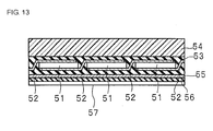
- FIG 13 is a sectional view which shows a structure of a solar cell module using the solar cells connected in series as shown in Figure 12 .
- a solar cell module in a solar cell module, plural solar cells 51 are connected in series through tabs 52.
- the solar cells 51 connected in such a fashion by the tabs 52 are sealed, for example, by a filler 53 consisting of an EVA (ethylene vinyl acetate) resin.
- a surface-protecting member 54 made of a surface-protecting transparent glass, is provided to overlie an upper surface (incidence plane side) of the filler 53.
- a surface-protecting member 57 made up of a sequence of a PET (polyethylene terephthalate) film, an aluminum foil and a PET film, for example, is provided to underlie a lower surface of the filler 53.
- Reference numeral 55 indicates a PET film for enhancing a pressure resistance of the solar cell.
- the large-area solar cell is divided into small-area solar cells which are subsequently arranged and electrically connected to fabricate a solar cell module.
- the utilization of the present invention can prevent cracking or the like that occurs when the large-area peripheral portion is removed by breaking and also reduce the incidence of defects.
- the projection forming members mounted to the breaking blade are shown to have the same height. With the projections of the same height, a stress is applied to the substrate by two stages to break it along the split groove.
- the present invention is not limited thereto. For example, those projections may have different heights. In such a case, breaking is achieved by applying a stress to the substrate by three or more stages.
- the projections are provided by the projection forming members mounted to the breaking blade.
- the present invention is not limited thereto.
- Those projections may be integrally formed with the breaking blade. In such a case, they may be formed by cutting the breaking blade, for example.
- the ring-shaped breaking blade is used to break the semiconductor substrate along the ring-shaped predetermined area which extends circumferentially of the substrate.
- the present invention is not limited thereto. The present invention can also be applied to the case where the semiconductor substrate is broken along a non-ring or linear predetermined area.
- a first breaking blade may be disposed in the location of each projection forming member 11, a second breaking blade in the location between neighboring projection forming members 11, 11, and the first and second breaking blades may be operated with a time delay in the performance of breaking.
- the solar cell is described as an example of the semiconductor substrate.
- the present invention is also applicable in breaking a semiconductor substrate other than the solar cell.
Landscapes
- Life Sciences & Earth Sciences (AREA)
- Forests & Forestry (AREA)
- Engineering & Computer Science (AREA)
- Mechanical Engineering (AREA)
- Dicing (AREA)
- Photovoltaic Devices (AREA)
- Mechanical Treatment Of Semiconductor (AREA)
Abstract
Description
- The present invention relates to a method and apparatus for breaking a semiconductor substrate, made by forming a photovoltaic element or other element structure on a silicon wafer or the like, along a predetermined region over which a split groove is formed, a method for breaking a solar cell utilizing the above method and apparatus, and a method for fabrication of a solar cell module.
- It has been conventionally studied to divide a solar cell comprising a large-area semiconductor substrate into small-area solar cells and connect them as by lead wires to thereby fabricate a solar cell module.
- In
Japanese Patent Laid-Open Nos. 2005-236017 2004-31839 - It is an object of the invention to provide a method and apparatus for breaking a semiconductor substrate, which can prevent the occurrence of cracking or the like due to stress concentration at a portion of the semiconductor substrate that is caused when the semidconductor substrate is broken along a predetermined area over which a split groove is formed, a method of breaking a solar cell utilizing the above method or apparatus, and a method for fabrication of a solar cell module.
- The method for breaking a semiconductor substrate, in accordance with the present invention, is a method in which a semiconductor substrate is broken along a predetermined area over which a split groove is formed, and is characterized as including the steps of holding the semiconductor substrate in position and pressing a portion of the semiconductor substrate outside the predetermined area to break the semiconductor substrate along the split groove, wherein the predetermined area has at least a neighboring pair of sides intersecting at an angle of less than 180 degrees and, when the semiconductor substrate is broken, one of the sides is pressed ahead of the other side.
- In the present invention, the predetermined area of the semiconductor substrate has at least a neighboring pair of sides intersecting at an angle of less than 180 degrees. Each of the neighboring, pair of sides may not be necessarily linear and may include a curve. They just need to intersect at an angle of less than 180 degrees. The reason why the intersecting angle is specified in the present invention as being less than 180 degrees is because a stress tends to concentrate at an edge portion where the two sides intersect at such an angle.
- In the present invention, one of such pair of sides is compressed ahead of the other in breaking the semiconductor substrate. This suppresses stress concentration at an edge portion defined by the pair of sides and accordingly prevents the occurrence of cracking or the like.
- That is, simultaneous application of a pressing force on the pair of sides, as conventionally practiced, causes stress concentration at the edge portion defined by the pair of sides and increases the occurrence of cracking or the like at such a portion. In the present invention, one side is compressed ahead of the other side. Accordingly, a stress is first exerted on the one side in its entirety so that breaking starts to occur along a scribed portion running over the one side. Subsequently, the stress is exerted on the other side in its entirety so that breaking starts to occur in the other side. The practice of such multi-stage breaking suppresses stress concentration at the edge portion where the one side meets with the other side and thus prevents the occurrence of cracking or the like.
- In the preferred embodiment according to the method of the present invention for breaking a semiconductor substrate, the portion of the semiconductor substrate inside the predetermined area is placed on a table. Thereafter, a breaking blade, located above the semiconductor substrate on the table, is moved downward to compress the portion of the semiconductor substrate outside the predetermined area so that the semiconductor substrate is broken along the split groove.
- The apparatus of the present invention for breaking a semiconductor substrate is an apparatus which utilizes the aforementioned method of the present invention to break the semiconductor substrate along the predetermined area over which the split groove is formed. The apparatus includes a table for placement of the portion of the semiconductor substrate inside the predetermined area and a breaking blade operable to move downward from a position above the semiconductor substrate placed on the table and compress the portion of the semiconductor substrate outside the predetermined area so that the semiconductor substrate is broken along the split groove. Characteristically, the predetermined area of the semiconductor substrate has at least a neighboring pair of sides intersecting at an angle of less than 180 degrees, and the breaking blade has a projection which, in breaking the semiconductor substrate, compresses a portion of the semiconductor substrate outside the one side so that the one side is compressed ahead of the other side.
- In the breaking apparatus of the present invention, the breaking blade has a projection which, when the semiconductor substrate is broken, compresses a portion of the semiconductor substrate outside the one side so that the one side is compressed ahead of the other side, as described above. By the action of the projection of the breaking blade, the one side is compressed ahead of the other side. This suppresses stress concentration at the edge portion where the one side meets the other side and prevents the occurrence of cracking or the like, as similar to the breaking method of the present invention.
- Preferably, the breaking apparatus of the present invention further includes a press member for pressing the portion of the semiconductor substrate inside the predetermined area against the table from above so that the semiconductor substrate is held firmly in position when it is broken. The provision of the press member makes it easy to firmly hold the semiconductor substrate placed on the table in position.
- In the present invention, a shape of the predetermined area defined by the split groove formed on the semiconductor substrate may be ring-like or linear such as a straight or curved line. In the case where the semiconductor substrate is broken into a ring-like shape by separating its circumferential portion as an undivided whole, a shape of the predetermined region defined by the split groove is ring-like. When the semiconductor substrate is broken along such a ring-shaped predetermined area, the breaking blade used is generally ring-shaped. In the case where the ring-shaped breaking blade is used, it preferably has a hole of a size that allows the table to pass therethrough.
- In the breaking apparatus of the present invention, an inner end face of the projection preferably has a taper that extends downwardly and outwardly. The provision of such a taper allows smooth bending of the portion of the semiconductor substrate outside the predetermined area, leading to breaking thereof along the split groove.
- Also in the present invention, a portion of the breaking blade that lacks the projection and exerts a pressure on the portion of the semiconductor substrate outside the predetermined area preferably has a taper which extends downwardly outwardly. The provision of such a taper allows smooth bending of the semiconductor substrate portion outside the predetermined area, leading to breaking thereof along the split groove.
- In the breaking apparatus of the present invention, the height of the projection is not particularly specified, but is generally preferably in the range of 0.5 - 50 mm, more preferably in the range of 1 - 10 mm.
- In the breaking apparatus of the present invention, the breaking blade, because of provision of the projections, has portions lacking the projection and those having the projection and can thus compress the semiconductor substrate by at least two stages. The projections may have different heights. In that case, the breaking blade can compress the semiconductor substrate by three or more stages, leading to breaking thereof.
- The breaking method and apparatus of the present invention is useful in removing a peripheral portion of a semiconductor substrate in the fabrication of a solar cell or in dividing a large-area semiconductor substrate into individual small-area solar cells. Accordingly, a semiconductor substrate having solar cell element structures formed thereon can be illustrated as one form of the semiconductor substrate for use in the present invention.
- According to the method of the present invention for fabrication of a solar cell module, a semiconductor substrate is broken using the breaking method or apparatus of the present invention. Therefore, the occurrence of cracking in breaking the semiconductor substrate can be prevented. As a result, a solar cell module can be fabricated with a good yield rate.
- The present invention can prevent the occurrence of cracking or the like due to stress concentration at a portion of the semiconductor substrate that is caused when the semiconductor substrate is broken along the predetermined area over which the split groove is formed.
-
-
Figure 1 is a side view, showing an embodiment of a breaking apparatus in accordance with the present invention; -
Figure 2 is an enlarged sectional view, showing a breaking blade portion to which a projection forming member is mounted; -
Figure 3 is a plain view, showing a breaking blade in the embodiment shown inFigure 1 , when viewed from below. -
Figure 4 is a plan view, showing a table in the embodiment shown inFigure 1 ; -
Figure 5 is a plain view, showing a press member in the embodiment shown inFigure 1 ; -
Figure 6 is a plain view, showing a solar cell before subjected to breaking; -
Figure 7 is a plain view, showing a solar cell after broken; -
Figure 8 is a partly enlarged sectional view, showing a predetermined area of a solar cell over which a split groove is formed; -
Figure 9 is a partly enlarged sectional view, showing a portion of the solar cell outside the predetermined area in the embodiment shown inFigure 1 , while in the process of being broken; -
Figure 10 is a plan view, showing solar cells after divided along dotted lines shown inFigure 7 ; -
Figure 11 is a plan view, showing an exemplary arrangement of solar cells ofFigure 10 obtained after division; -
Figure 12 is a schematic sectional view, showing solar cells connected in series by tabs; and -
Figure 13 is a sectional view, showing an embodiment of a solar cell module as fabricated in accordance with the present invention. -
Figure 1 is a side view which shows an embodiment of an apparatus for breaking a semiconductor substrate in accordance with the present invention. - Referring to
Figure 1 , asemiconductor substrate 1 is placed on a table 20 and held in position by apress member 30 which is supported from above by arod 31 and compresses the substrate against the table 20. The table 20 is supported from below byrods 21. The method by which the semiconductor substrate is held in position is not limited thereto. - Located above the
semiconductor substrate 1 is abreaking blade 11. Thebreaking blade 10 is ring-shaped and has an interiorcentral hole 10b which is sized to allow passage of thepress member 30 and the table 20. Aprojection forming member 11 is attached to an inner portion of a lower face of the ring-shapedbreaking blade 10. Although not shown, thebreaking blade 10 is supported from above by rods for vertical movement. -
Figure 2 is an enlarged sectional view which shows thebreaking blade 10 and theprojection forming member 11.Figure 3 is a plan view which shows a lower face of thebreaking blade 10. As shown inFigures 2 and3 , an inner end face of theprojection forming member 11 has ataper 11a which extends downwardly and outwardly. - As shown in
Figure 3 , the interior hole 10a of thebreaking blade 10 has a generally dodecagonal shape. Theprojection forming member 11 is mounted to every other side and accordingly to six sides in total. An inner end surface of the breaking blade, where theprojection forming members 11 are not mounted, has a taper 10a at its lower portion. This taper 10a is configured to extend downwardly and outwardly, as similar to thetaper 11a of theprojection forming member 11. - The
breaking blade 10 has circumferentially arranged threeholes 12 for passage of rods which together support the breaking blade from above. - As described above, the
central hole 10b of thebreaking blade 10 has a generally dodecagonal shape. The one side to which theprojection forming member 11 is mounted and the adjacent side to which theprojection forming member 11 is not mounted intersect at an angle of less than 180 degrees. In this embodiment, the neighboring pair of sides are shown to intersect at an angle of about 160 degrees. Although the side to which theprojection forming member 11 is not mounted appears somewhat rounded, its end portions meet the respective adjacent sides each contiguous with an inner end of theprojection formingmember 11 at an angle of less than 180 degrees, as specified in the present invention. - The height of the
projection forming member 11, that is, the height h of the projection in this embodiment, as shown inFigure 2 , is 3 mm. The height of the projection in the present invention can be suitably set up considering a rate of movement of the breaking blade and others. However, it is generally preferably in the range of 1 - 10 mm, as described above. -
Figure 4 is plan view which shows the table 20. As shown inFigure 4 , the table is sized to pass through thehole 10b of thebreaking blade 10 and has a shape analogous to that of thehole 10b. Preferably, the respective shapes of thehole 10b of thebreaking blade 10 and the table 20 nearly correspond to the shape of the predetermined area along which the split groove is formed in the semiconductor substrate. - The table 20 has a
central hole 20a for passage of therods 21 shown inFigure 1 for supporting the table 20. -
Figure 5 is a plan view which shows thepress member 30 shown inFigure 1 . Preferably, thepress member 30 is also sized to pass through the hole 10a of thebreaking blade 10 and has a shape contiguous to that of the hole 10a. - Although the
breaking blade 10,projection forming member 11 and table 20 are not particularly specified in material type, they are all made of stainless steel in this embodiment. Also, the material type of the press member shown inFigure 5 is not particularly specified. However, in this embodiment, it is formed of an engineering plastic or other plastic member. - Also, the respective material types of the rods for supporting the
breaking blade 10, table 20 andpress member 30 are not particularly specified. However, they are all made of stainless steel in this embodiment. -
Figure 6 is a plan view which shows thesemiconductor substrate 1 as it is used in a solar cell. Thesolar cell 1 has a current collecting electrode 1a and a ring-shapedpredetermined area 2 extending along its outer periphery. -
Figure 8 is an enlarged sectional area which shows thepredetermined area 2 in thesolar cell 1 and its surroundings. Asplit groove 3 is formed over thepredetermined area 2 in thesolar cell 1. Thesplit groove 3 can be formed, for example, by irradiating the solar cell with an energy beam such as a laser beam. Examples of useful lasers include a YAG laser, gas lasers such as a CO2 laser, KrF laser, ArF laser and XeCl laser, and solid lasers such as an YVO4 laser. Although not particularly specified, the depth d of thesplit groove 3 is preferably 35 - 70 % of the thickness T of the solar cell (semiconductor substrate) 1. - In the
solar cell 1 shown inFigure 8 , its lower surface constitutes a primary light-receiving surface. Deposited on a lower surface of an n-type singlecrystal silicon substrate 4 is an i-type amorphous silicon layer 5i (about 5 nm - about 20 nm thick) on which a p-typeamorphous silicon layer 5p (about 5 nm - about 20 nm thick) is deposited. These constitute a semiconductor junction region which is a pin junction. A transparent electroconductive film 6 (about 30 nm - about 150 nm thick) such as of ITO (indium tin oxide) is deposited on the p-typeamorphous silicon layer 5p. - An i-type amorphous silicon layer 7i (about 5 nm - about 20 nm thick) and an n-type
amorphous silicon layer 7n (about 5 nm - about 20 nm thick) are sequentially stacked on an upper surface of the n-type singlecrystal silicon substrate 4. A transparent electroconductive film 8 (about 30 nm - about 150 nm thick) is formed on the n-typeamorphous silicon layer 7n. - In the above solar cell, a pn junction is formed between the n-type single
crystal silicon substrate 4 and the p-typeamorphous silicon layer 5p. Inserted into the junction interface is the i-type amorphous silicon layer 5i having a level of thickness that does not contribute to power generation. - In this embodiment, the n-type single crystal silicon substrate is used. Alternatively, a p-type single crystal silicon substrate may be used. In such a case, an i-type amorphous silicon layer and an n-type amorphous silicon layer may be deposited on a lower surface of the substrate, and an i-type amorphous silicon layer and a p-type amorphous silicon layer may be deposited on an upper surface of the substrate. Alternatively, a surface of an n-type or p-type crystalline semiconductor substrate may be doped with a p-type or n-type dopant to form a pn junction for a solar cell. The present invention is also applicable to semiconductor substrates other than the solar cell.
- Referring to
Figure 6 , thepredetermined area 2 in thesolar cell 1 is defined by thesplit groove 3 shown inFigure 8 . - Referring to
Figure 1 , thesolar cell 1 is placed on the table 20 such that a portion of thesolar cell 1 inside thepredetermined area 2 is positioned over the table. Thepress member 30 is then moved to ride on thepredetermined area 2 in thesolar cell 1 and compresses thesolar cell 1 downward so that thesolar cell 1 is held firmly in position. - Referring to
Figure 1 , thebreaking blade 10 is then moved downward. During its downward movement, thepress member 30 is allowed to pass through thehole 10b. Subsequently, theprojection forming member 11 mounted to the lower face of thebreaking blade 10 is brought into contact with a portion of the solar cell that extends outwardly from the table 20 andpress member 30. -
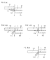
Figure 9 is a sectional view which shows thesolar cell 1 in the process of being broken by the breaking blade along thepredetermined area 3 over which thesplit groove 3 is formed. - As shown in
Figure 9(a) , as thebreaking blade 10 moves downward, theprojection forming members 11 mounted to the lower face of thebreaking blade 10 first contact with the corresponding portions of thesolar cell 1 outside thepredetermined area 2. - As the
breaking blade 10 further moves downward, such portions of thesolar cell 1 outside thepredetermined area 2 are pushed downward and bent to start breaking along thesplit groove 3, as shown inFigure 9(b) . - At this point, the remaining portions of the
solar cell 1 outside the predetermined area have not been pushed downward yet and remain unbroken, as shown inFigure 9(c) , because the breaking blade does not carry theprojection forming members 11 in the corresponding portions. - As the breaking blade further moves downward, such remaining portions of the
solar cell 1 outside thepredetermined area 2 are also pushed downward and bent to start breaking along thesplit groove 3, as shown inFigure 9(d) . - As described above, in this embodiment, the portions of the breaking blade that mount the
projection forming members 11 start to break the corresponding portions of the solar cell along thesplit groove 3. Thereafter, the remaining portions of the breaking blade that do not mount theprojection forming members 11 start to break the corresponding portions of the solar cell along thesplit groove 3. As such, a stress is exerted on one side of a neighboring pair of sides in the predetermined area to achieve breaking. Subsequently, a stress is exerted on the other side to achieve breaking. This suppresses stress concentration that occurs at an edge portion of the pair of sides when a stress is simultaneously exerted on both sides. Thus, the present invention can prevent cracking that occurs when the semiconductor substrate is broken along the split groove. -
Figure 7 is a plan view which shows the configuration of thesolar cell 1 after broken along thepredetermined area 2 and separated from the peripheral portion. After removal of the peripheral useless portion, thesolar cell 1 is further divided along planes shown by dotted lines inFigure 7 . In this case, division is achieved by forming split grooves over such planes in the same manner as described above and then bending and breaking the substrate along the split grooves. Since the substrate is broken along linear lines, the multi-stage application of a stress is not required for the breaking. A sequence of breaking is not particularly specified. For example, the solar cell can be first broken along the longitudinally split groove into two individual solar cells. Each individual solar cell can be further bent and broken along the laterally split groove. -
Figure 10 is a plan view which shows the individual solar cells after division. As shown inFigure 10 , the solar cell is divided into four individual small-areasolar cells - Breaking of the solar cell is preferably carried out subsequent to formation of a pn junction in the semiconductor substrate. Because there is a possibility that breaking leaves a minute defect on a broken surface of the semiconductor substrate, if the pn junction is formed after the breaking, an yielding rate or performance characteristics of the solar cell may decrease or deteriorate. In order to avoid such disadvantages, a breaking process is preferably performed after formation of the pn junction.
-
Figure 12 is a sectional view shows plural solar cells connected in series by tabs. As shown inFigure 12 , they can be connected in series by connecting an upper-surface electrode of asolar cell 51 to a lower-surface electrode of a neighboringsolar cell 51 by atab 52. -
Figure 13 is a sectional view which shows a structure of a solar cell module using the solar cells connected in series as shown inFigure 12 . As shown inFigure 13 , in a solar cell module, pluralsolar cells 51 are connected in series throughtabs 52. Thesolar cells 51 connected in such a fashion by thetabs 52 are sealed, for example, by afiller 53 consisting of an EVA (ethylene vinyl acetate) resin. A surface-protectingmember 54, made of a surface-protecting transparent glass, is provided to overlie an upper surface (incidence plane side) of thefiller 53. Also, a surface-protectingmember 57, made up of a sequence of a PET (polyethylene terephthalate) film, an aluminum foil and a PET film, for example, is provided to underlie a lower surface of thefiller 53.Reference numeral 55 indicates a PET film for enhancing a pressure resistance of the solar cell. - As described above, after removal of the peripheral useless portion, the large-area solar cell is divided into small-area solar cells which are subsequently arranged and electrically connected to fabricate a solar cell module. In the fabrication of the solar cell module, the utilization of the present invention can prevent cracking or the like that occurs when the large-area peripheral portion is removed by breaking and also reduce the incidence of defects.
- In the above embodiment, the projection forming members mounted to the breaking blade are shown to have the same height. With the projections of the same height, a stress is applied to the substrate by two stages to break it along the split groove. However, the present invention is not limited thereto. For example, those projections may have different heights. In such a case, breaking is achieved by applying a stress to the substrate by three or more stages.
- Also, in the above embodiment, the projections are provided by the projection forming members mounted to the breaking blade. However, the present invention is not limited thereto. Those projections may be integrally formed with the breaking blade. In such a case, they may be formed by cutting the breaking blade, for example.
- Also, in the above embodiment, the ring-shaped breaking blade is used to break the semiconductor substrate along the ring-shaped predetermined area which extends circumferentially of the substrate. However, the present invention is not limited thereto. The present invention can also be applied to the case where the semiconductor substrate is broken along a non-ring or linear predetermined area.
- Also, the breaking method of the present invention can be carried out using the other apparatus. For example, in
Figure 3 , a first breaking blade may be disposed in the location of eachprojection forming member 11, a second breaking blade in the location between neighboringprojection forming members - Also, in the above embodiment, the solar cell is described as an example of the semiconductor substrate. However, the present invention is also applicable in breaking a semiconductor substrate other than the solar cell.
Claims (10)
- A method for breaking a semiconductor substrate along a predetermined area over which a split groove is formed, comprising the steps of:holding said semiconductor substrate in position; andcompressing a portion of the semiconductor substrate outside the predetermined area to break the semiconductor substrate along said split groove;wherein said predetermined area has at least a neighboring pair of sides intersecting at an angle of less than 180 degrees and, in breaking the semiconductor substrate, one of said pair of sides is compressed ahead of the other side.
- The method for breaking a semiconductor substrate as recited in claim 1, wherein, subsequent to placement of a portion of the semiconductor substrate inside the predetermined area on a table, a breaking blade located above the semiconductor substrate is moved downward to compress the portion of the semiconductor substrate outside the predetermined area so that the semiconductor substrate is broken along the split groove.
- An apparatus for breaking a semiconductor substrate along a predetermined area over which a split groove is formed, comprising:a table for placement of a portion of said semiconductor substrate inside said predetermined area; anda breaking blade being operable to move downward from a position above the semiconductor substrate placed on the table to thereby compress the portion of the semiconductor substrate outside the predetermined area so that the semiconductor substrate is broken along the split groove;wherein the predetermined area of the semiconductor substrate has at least a neighboring pair of sides intersecting at an angle of less than 180 degrees, and said breaking blade has a projection which, in breaking the semiconductor substrate, compresses a portion of the semiconductor substrate outside the one side so that the one side is compressed ahead of the other side.
- The apparatus for breaking a semiconductor substrate as recited in claim 3, further comprising a press member for compressing the portion of the semiconductor substrate inside the predetermined area against the table from above so that the semiconductor substrate is held in position when it is broken.
- The apparatus for breaking a semiconductor substrate as recited in claim 3 or 4, wherein said breaking blade is ring-shaped and has an interior central hole sized to allow passage of said table.
- The apparatus for breaking a semiconductor substrate as recited in any one of claims 3 - 5, wherein an inner end face of said projection has a taper that extends downwardly and outwardly.
- The apparatus for breaking a semiconductor substrate as recited in any one of claims 3 - 5, wherein said semiconductor substrate has a solar cell element structure formed thereon.
- A method for breaking a solar cell comprising the steps of:forming a pn junction on a semiconductor substrate of one conductive type;forming a split groove in said semiconductor substrate; andbreaking the semiconductor substrate along a predetermined area over which said split groove is formed;wherein said predetermined area of the semiconductor substrate has at least a neighboring pair of sides intersecting at an angle of less than 180 degrees and, in breaking the semiconductor substrate, one side is compressed ahead of the other side.
- The method for breaking a solar cell as recited in claim 8, wherein, subsequent to forming said pn junction on the semiconductor substrate, the semiconductor substrate is broken.
- A method for fabrication of a solar cell module comprising the steps of:providing a semiconductor substrate having a solar cell element structure formed thereon;dividing said semiconductor substrate using the method recited in claim 1, 2, 8 or 9 or the apparatus recited in any one of claims 3 - 7; andarranging plural semiconductor substrates after division and electrically connecting them to thereby fabricate a solar cell module.
Applications Claiming Priority (1)
| Application Number | Priority Date | Filing Date | Title |
|---|---|---|---|
| JP2006348789A JP5147230B2 (en) | 2006-12-26 | 2006-12-26 | Semiconductor substrate cleaving apparatus and solar cell module manufacturing method |
Publications (3)
| Publication Number | Publication Date |
|---|---|
| EP1939948A2 true EP1939948A2 (en) | 2008-07-02 |
| EP1939948A3 EP1939948A3 (en) | 2010-11-17 |
| EP1939948B1 EP1939948B1 (en) | 2012-09-26 |
Family
ID=39271311
Family Applications (1)
| Application Number | Title | Priority Date | Filing Date |
|---|---|---|---|
| EP20070025018 Not-in-force EP1939948B1 (en) | 2006-12-26 | 2007-12-21 | Method and apparatus for breaking semiconductor substrate |
Country Status (3)
| Country | Link |
|---|---|
| US (1) | US8034653B2 (en) |
| EP (1) | EP1939948B1 (en) |
| JP (1) | JP5147230B2 (en) |
Families Citing this family (5)
| Publication number | Priority date | Publication date | Assignee | Title |
|---|---|---|---|---|
| JP5059628B2 (en) * | 2008-01-10 | 2012-10-24 | 株式会社日立製作所 | Semiconductor device |
| JP2012256738A (en) * | 2011-06-09 | 2012-12-27 | Mitsubishi Electric Corp | Manufacturing method of photovoltaic device |
| US9899546B2 (en) | 2014-12-05 | 2018-02-20 | Tesla, Inc. | Photovoltaic cells with electrodes adapted to house conductive paste |
| US9685579B2 (en) | 2014-12-05 | 2017-06-20 | Solarcity Corporation | Photovoltaic structure cleaving system |
| WO2018166598A1 (en) * | 2017-03-16 | 2018-09-20 | Applied Materials Italia S.R.L. | Apparatus for use in the manufacture of a solar cell arrangement, system for manufacture of at least one shingled solar cell arrangement, and method for separating a solar cell into two or more solar cell pieces |
Citations (2)
| Publication number | Priority date | Publication date | Assignee | Title |
|---|---|---|---|---|
| JP2004031839A (en) | 2002-06-27 | 2004-01-29 | Sanyo Electric Co Ltd | Method for manufacturing solar battery module and method for separating solar battery cell |
| JP2005236017A (en) | 2004-02-19 | 2005-09-02 | Sharp Corp | Method for manufacturing solar battery cell |
Family Cites Families (17)
| Publication number | Priority date | Publication date | Assignee | Title |
|---|---|---|---|---|
| JPS6282008A (en) * | 1985-10-04 | 1987-04-15 | 三菱電機株式会社 | Breaking device for semiconductor wafer |
| JPS62105446A (en) * | 1985-10-31 | 1987-05-15 | Sharp Corp | Manufacture of semiconductor device |
| JPS62108007A (en) * | 1985-11-07 | 1987-05-19 | 富士電機株式会社 | Method of dividing semiconductor board |
| JPS6416610A (en) * | 1987-07-10 | 1989-01-20 | Nippon Mining Co | Cleaving device |
| JPH01178408A (en) * | 1988-01-07 | 1989-07-14 | Fujitsu Ltd | Dividing method for printed wiring board |
| JPH02127003A (en) * | 1988-11-07 | 1990-05-15 | Nec Corp | Split jig for wafer |
| JPH02179708A (en) * | 1989-01-05 | 1990-07-12 | Kawasaki Steel Corp | Break separating method of semi-conductor wafer |
| JP3349318B2 (en) * | 1995-11-27 | 2002-11-25 | 三洋電機株式会社 | Solar cell module |
| US6962279B1 (en) * | 2000-10-18 | 2005-11-08 | Ge Medical Systems Global Technology Company, Llc | Apparatus and method for glass separation for flat panel displays |
| JP2002252187A (en) * | 2001-02-27 | 2002-09-06 | Mitsubishi Electric Corp | Semiconductor wafer cutting device and semiconductor wafer cutting method using the same |
| JP2003286044A (en) * | 2002-03-27 | 2003-10-07 | Sharp Corp | Substrate cutting device and substrate cutting method |
| US20060278956A1 (en) * | 2003-03-13 | 2006-12-14 | Pdf Solutions, Inc. | Semiconductor wafer with non-rectangular shaped dice |
| JP3868940B2 (en) * | 2003-09-03 | 2007-01-17 | テクダイヤ株式会社 | Scribing tool and its holder and apparatus |
| JP4515790B2 (en) * | 2004-03-08 | 2010-08-04 | 株式会社東芝 | Semiconductor device manufacturing method and manufacturing apparatus thereof |
| JP4694795B2 (en) * | 2004-05-18 | 2011-06-08 | 株式会社ディスコ | Wafer division method |
| KR101126059B1 (en) * | 2004-09-03 | 2012-04-12 | 신에쯔 한도타이 가부시키가이샤 | Photovoltaic power generation module and photovoltaic power generation system employing it |
| JP5100971B2 (en) * | 2005-03-10 | 2012-12-19 | 三菱重工業株式会社 | Manufacturing method of solar cell panel |
-
2006
- 2006-12-26 JP JP2006348789A patent/JP5147230B2/en not_active Expired - Fee Related
-
2007
- 2007-12-21 EP EP20070025018 patent/EP1939948B1/en not_active Not-in-force
- 2007-12-26 US US11/964,405 patent/US8034653B2/en not_active Expired - Fee Related
Patent Citations (2)
| Publication number | Priority date | Publication date | Assignee | Title |
|---|---|---|---|---|
| JP2004031839A (en) | 2002-06-27 | 2004-01-29 | Sanyo Electric Co Ltd | Method for manufacturing solar battery module and method for separating solar battery cell |
| JP2005236017A (en) | 2004-02-19 | 2005-09-02 | Sharp Corp | Method for manufacturing solar battery cell |
Also Published As
| Publication number | Publication date |
|---|---|
| EP1939948B1 (en) | 2012-09-26 |
| JP2008159959A (en) | 2008-07-10 |
| EP1939948A3 (en) | 2010-11-17 |
| US20080213979A1 (en) | 2008-09-04 |
| JP5147230B2 (en) | 2013-02-20 |
| US8034653B2 (en) | 2011-10-11 |
Similar Documents
| Publication | Publication Date | Title |
|---|---|---|
| US8946547B2 (en) | Backplane reinforcement and interconnects for solar cells | |
| US8389320B2 (en) | Method for fracturing semiconductor substrate, method for fracturing solar cell, and the solar cell | |
| CN205984934U (en) | A equipment for cutting apart photovoltaic structure | |
| CN104051581B (en) | Solar cell laser scribing methods | |
| US11063170B2 (en) | Two-step hole etching process | |
| KR102015591B1 (en) | Active backplane for thin silicon solar cells | |
| JP5328363B2 (en) | Method for manufacturing solar cell element and solar cell element | |
| JP5458485B2 (en) | Method for manufacturing solar cell and method for manufacturing solar cell module | |
| US8034653B2 (en) | Method and apparatus for breaking semiconductor substrate, method for breaking solar cell and method for fabrication of solar cell module | |
| KR20140064854A (en) | High-efficiency solar photovoltaic cells and modules using thin crystalline semiconductor absorbers | |
| US7755157B2 (en) | Photovoltaic device and manufacturing method of photovoltaic device | |
| CN101517747A (en) | Solar cell module | |
| JP2006310774A (en) | Photovoltaic element and method for manufacturing the same | |
| JP4773543B2 (en) | Solar cell module with edge space | |
| Van Nieuwenhuysen et al. | High quality epitaxial foils, obtained by a porous silicon based layer transfer process, for integration in back contacted solar cells | |
| JP2010010606A (en) | Optical conversion element cell, integrated optical conversion device, method of manufacturing optical conversion element cell, and method of manufacturing integratedoptical conversion device | |
| CN105990467A (en) | Method for manufacturing thin film solar cell | |
| JP5183343B2 (en) | Semiconductor wafer manufacturing method and solar cell manufacturing method | |
| JP2001267618A (en) | Manufacturing method of integrated thin film photoelectric conversion device | |
| JP4542508B2 (en) | Vertical light emitting diode and manufacturing method thereof | |
| JP5134075B2 (en) | Method for manufacturing thin film solar cell | |
| JP3776098B2 (en) | Photovoltaic generator | |
| JP4986087B2 (en) | Thin film solar cell and manufacturing method thereof | |
| JP3754431B2 (en) | Photovoltaic generator | |
| TWM526188U (en) | Solar cell unit arrangement structure |
Legal Events
| Date | Code | Title | Description |
|---|---|---|---|
| PUAI | Public reference made under article 153(3) epc to a published international application that has entered the european phase |
Free format text: ORIGINAL CODE: 0009012 |
|
| AK | Designated contracting states |
Kind code of ref document: A2 Designated state(s): AT BE BG CH CY CZ DE DK EE ES FI FR GB GR HU IE IS IT LI LT LU LV MC MT NL PL PT RO SE SI SK TR |
|
| AX | Request for extension of the european patent |
Extension state: AL BA HR MK RS |
|
| PUAL | Search report despatched |
Free format text: ORIGINAL CODE: 0009013 |
|
| AK | Designated contracting states |
Kind code of ref document: A3 Designated state(s): AT BE BG CH CY CZ DE DK EE ES FI FR GB GR HU IE IS IT LI LT LU LV MC MT NL PL PT RO SE SI SK TR |
|
| AX | Request for extension of the european patent |
Extension state: AL BA HR MK RS |
|
| RIC1 | Information provided on ipc code assigned before grant |
Ipc: H01L 21/00 20060101ALI20101008BHEP Ipc: H01L 31/18 20060101AFI20080414BHEP |
|
| 17P | Request for examination filed |
Effective date: 20110516 |
|
| AKX | Designation fees paid |
Designated state(s): AT BE BG CH CY CZ DE DK EE ES FI FR GB GR HU IE IS IT LI LT LU LV MC MT NL PL PT RO SE SI SK TR |
|
| RIC1 | Information provided on ipc code assigned before grant |
Ipc: H01L 21/8256 20060101ALI20120307BHEP Ipc: H01L 31/18 20060101AFI20120307BHEP Ipc: H01L 21/67 20060101ALI20120307BHEP |
|
| RTI1 | Title (correction) |
Free format text: METHOD AND APPARATUS FOR BREAKING SEMICONDUCTOR SUBSTRATE |
|
| GRAP | Despatch of communication of intention to grant a patent |
Free format text: ORIGINAL CODE: EPIDOSNIGR1 |
|
| GRAS | Grant fee paid |
Free format text: ORIGINAL CODE: EPIDOSNIGR3 |
|
| GRAA | (expected) grant |
Free format text: ORIGINAL CODE: 0009210 |
|
| AK | Designated contracting states |
Kind code of ref document: B1 Designated state(s): AT BE BG CH CY CZ DE DK EE ES FI FR GB GR HU IE IS IT LI LT LU LV MC MT NL PL PT RO SE SI SK TR |
|
| REG | Reference to a national code |
Ref country code: GB Ref legal event code: FG4D |
|
| REG | Reference to a national code |
Ref country code: CH Ref legal event code: EP |
|
| REG | Reference to a national code |
Ref country code: AT Ref legal event code: REF Ref document number: 577379 Country of ref document: AT Kind code of ref document: T Effective date: 20121015 |
|
| REG | Reference to a national code |
Ref country code: IE Ref legal event code: FG4D |
|
| REG | Reference to a national code |
Ref country code: DE Ref legal event code: R096 Ref document number: 602007025667 Country of ref document: DE Effective date: 20121115 |
|
| PG25 | Lapsed in a contracting state [announced via postgrant information from national office to epo] |
Ref country code: FI Free format text: LAPSE BECAUSE OF FAILURE TO SUBMIT A TRANSLATION OF THE DESCRIPTION OR TO PAY THE FEE WITHIN THE PRESCRIBED TIME-LIMIT Effective date: 20120926 Ref country code: LT Free format text: LAPSE BECAUSE OF FAILURE TO SUBMIT A TRANSLATION OF THE DESCRIPTION OR TO PAY THE FEE WITHIN THE PRESCRIBED TIME-LIMIT Effective date: 20120926 |
|
| REG | Reference to a national code |
Ref country code: AT Ref legal event code: MK05 Ref document number: 577379 Country of ref document: AT Kind code of ref document: T Effective date: 20120926 |
|
| REG | Reference to a national code |
Ref country code: LT Ref legal event code: MG4D Effective date: 20120926 |
|
| REG | Reference to a national code |
Ref country code: NL Ref legal event code: VDEP Effective date: 20120926 |
|
| PG25 | Lapsed in a contracting state [announced via postgrant information from national office to epo] |
Ref country code: GR Free format text: LAPSE BECAUSE OF FAILURE TO SUBMIT A TRANSLATION OF THE DESCRIPTION OR TO PAY THE FEE WITHIN THE PRESCRIBED TIME-LIMIT Effective date: 20121227 Ref country code: SE Free format text: LAPSE BECAUSE OF FAILURE TO SUBMIT A TRANSLATION OF THE DESCRIPTION OR TO PAY THE FEE WITHIN THE PRESCRIBED TIME-LIMIT Effective date: 20120926 Ref country code: LV Free format text: LAPSE BECAUSE OF FAILURE TO SUBMIT A TRANSLATION OF THE DESCRIPTION OR TO PAY THE FEE WITHIN THE PRESCRIBED TIME-LIMIT Effective date: 20120926 Ref country code: SI Free format text: LAPSE BECAUSE OF FAILURE TO SUBMIT A TRANSLATION OF THE DESCRIPTION OR TO PAY THE FEE WITHIN THE PRESCRIBED TIME-LIMIT Effective date: 20120926 |
|
| PG25 | Lapsed in a contracting state [announced via postgrant information from national office to epo] |
Ref country code: EE Free format text: LAPSE BECAUSE OF FAILURE TO SUBMIT A TRANSLATION OF THE DESCRIPTION OR TO PAY THE FEE WITHIN THE PRESCRIBED TIME-LIMIT Effective date: 20120926 Ref country code: BE Free format text: LAPSE BECAUSE OF FAILURE TO SUBMIT A TRANSLATION OF THE DESCRIPTION OR TO PAY THE FEE WITHIN THE PRESCRIBED TIME-LIMIT Effective date: 20120926 Ref country code: NL Free format text: LAPSE BECAUSE OF FAILURE TO SUBMIT A TRANSLATION OF THE DESCRIPTION OR TO PAY THE FEE WITHIN THE PRESCRIBED TIME-LIMIT Effective date: 20120926 Ref country code: ES Free format text: LAPSE BECAUSE OF FAILURE TO SUBMIT A TRANSLATION OF THE DESCRIPTION OR TO PAY THE FEE WITHIN THE PRESCRIBED TIME-LIMIT Effective date: 20130106 Ref country code: CZ Free format text: LAPSE BECAUSE OF FAILURE TO SUBMIT A TRANSLATION OF THE DESCRIPTION OR TO PAY THE FEE WITHIN THE PRESCRIBED TIME-LIMIT Effective date: 20120926 Ref country code: IS Free format text: LAPSE BECAUSE OF FAILURE TO SUBMIT A TRANSLATION OF THE DESCRIPTION OR TO PAY THE FEE WITHIN THE PRESCRIBED TIME-LIMIT Effective date: 20130126 Ref country code: RO Free format text: LAPSE BECAUSE OF FAILURE TO SUBMIT A TRANSLATION OF THE DESCRIPTION OR TO PAY THE FEE WITHIN THE PRESCRIBED TIME-LIMIT Effective date: 20120926 |
|
| PG25 | Lapsed in a contracting state [announced via postgrant information from national office to epo] |
Ref country code: PL Free format text: LAPSE BECAUSE OF FAILURE TO SUBMIT A TRANSLATION OF THE DESCRIPTION OR TO PAY THE FEE WITHIN THE PRESCRIBED TIME-LIMIT Effective date: 20120926 Ref country code: CY Free format text: LAPSE BECAUSE OF FAILURE TO SUBMIT A TRANSLATION OF THE DESCRIPTION OR TO PAY THE FEE WITHIN THE PRESCRIBED TIME-LIMIT Effective date: 20120926 Ref country code: SK Free format text: LAPSE BECAUSE OF FAILURE TO SUBMIT A TRANSLATION OF THE DESCRIPTION OR TO PAY THE FEE WITHIN THE PRESCRIBED TIME-LIMIT Effective date: 20120926 Ref country code: PT Free format text: LAPSE BECAUSE OF FAILURE TO SUBMIT A TRANSLATION OF THE DESCRIPTION OR TO PAY THE FEE WITHIN THE PRESCRIBED TIME-LIMIT Effective date: 20130128 |
|
| PG25 | Lapsed in a contracting state [announced via postgrant information from national office to epo] |
Ref country code: AT Free format text: LAPSE BECAUSE OF FAILURE TO SUBMIT A TRANSLATION OF THE DESCRIPTION OR TO PAY THE FEE WITHIN THE PRESCRIBED TIME-LIMIT Effective date: 20120926 |
|
| PG25 | Lapsed in a contracting state [announced via postgrant information from national office to epo] |
Ref country code: DK Free format text: LAPSE BECAUSE OF FAILURE TO SUBMIT A TRANSLATION OF THE DESCRIPTION OR TO PAY THE FEE WITHIN THE PRESCRIBED TIME-LIMIT Effective date: 20120926 Ref country code: BG Free format text: LAPSE BECAUSE OF FAILURE TO SUBMIT A TRANSLATION OF THE DESCRIPTION OR TO PAY THE FEE WITHIN THE PRESCRIBED TIME-LIMIT Effective date: 20121226 Ref country code: MC Free format text: LAPSE BECAUSE OF NON-PAYMENT OF DUE FEES Effective date: 20121231 |
|
| REG | Reference to a national code |
Ref country code: CH Ref legal event code: PL |
|
| PLBE | No opposition filed within time limit |
Free format text: ORIGINAL CODE: 0009261 |
|
| STAA | Information on the status of an ep patent application or granted ep patent |
Free format text: STATUS: NO OPPOSITION FILED WITHIN TIME LIMIT |
|
| GBPC | Gb: european patent ceased through non-payment of renewal fee |
Effective date: 20121226 |
|
| PG25 | Lapsed in a contracting state [announced via postgrant information from national office to epo] |
Ref country code: IT Free format text: LAPSE BECAUSE OF FAILURE TO SUBMIT A TRANSLATION OF THE DESCRIPTION OR TO PAY THE FEE WITHIN THE PRESCRIBED TIME-LIMIT Effective date: 20120926 |
|
| 26N | No opposition filed |
Effective date: 20130627 |
|
| REG | Reference to a national code |
Ref country code: IE Ref legal event code: MM4A |
|
| REG | Reference to a national code |
Ref country code: FR Ref legal event code: ST Effective date: 20130830 |
|
| REG | Reference to a national code |
Ref country code: DE Ref legal event code: R097 Ref document number: 602007025667 Country of ref document: DE Effective date: 20130627 |
|
| PG25 | Lapsed in a contracting state [announced via postgrant information from national office to epo] |
Ref country code: CH Free format text: LAPSE BECAUSE OF NON-PAYMENT OF DUE FEES Effective date: 20121231 Ref country code: LI Free format text: LAPSE BECAUSE OF NON-PAYMENT OF DUE FEES Effective date: 20121231 Ref country code: IE Free format text: LAPSE BECAUSE OF NON-PAYMENT OF DUE FEES Effective date: 20121221 |
|
| PG25 | Lapsed in a contracting state [announced via postgrant information from national office to epo] |
Ref country code: FR Free format text: LAPSE BECAUSE OF NON-PAYMENT OF DUE FEES Effective date: 20130102 Ref country code: GB Free format text: LAPSE BECAUSE OF NON-PAYMENT OF DUE FEES Effective date: 20121226 Ref country code: MT Free format text: LAPSE BECAUSE OF FAILURE TO SUBMIT A TRANSLATION OF THE DESCRIPTION OR TO PAY THE FEE WITHIN THE PRESCRIBED TIME-LIMIT Effective date: 20120926 |
|
| PG25 | Lapsed in a contracting state [announced via postgrant information from national office to epo] |
Ref country code: TR Free format text: LAPSE BECAUSE OF FAILURE TO SUBMIT A TRANSLATION OF THE DESCRIPTION OR TO PAY THE FEE WITHIN THE PRESCRIBED TIME-LIMIT Effective date: 20120926 |
|
| PG25 | Lapsed in a contracting state [announced via postgrant information from national office to epo] |
Ref country code: LU Free format text: LAPSE BECAUSE OF NON-PAYMENT OF DUE FEES Effective date: 20121221 |
|
| PG25 | Lapsed in a contracting state [announced via postgrant information from national office to epo] |
Ref country code: HU Free format text: LAPSE BECAUSE OF FAILURE TO SUBMIT A TRANSLATION OF THE DESCRIPTION OR TO PAY THE FEE WITHIN THE PRESCRIBED TIME-LIMIT Effective date: 20071221 |
|
| PGFP | Annual fee paid to national office [announced via postgrant information from national office to epo] |
Ref country code: DE Payment date: 20211027 Year of fee payment: 15 |
|
| REG | Reference to a national code |
Ref country code: DE Ref legal event code: R119 Ref document number: 602007025667 Country of ref document: DE |
|
| PG25 | Lapsed in a contracting state [announced via postgrant information from national office to epo] |
Ref country code: DE Free format text: LAPSE BECAUSE OF NON-PAYMENT OF DUE FEES Effective date: 20230701 |