EP1933364A2 - Method and apparatus for preventing arcing at ports exposed to a plasma in plasma processing chambers - Google Patents
Method and apparatus for preventing arcing at ports exposed to a plasma in plasma processing chambers Download PDFInfo
- Publication number
- EP1933364A2 EP1933364A2 EP07122850A EP07122850A EP1933364A2 EP 1933364 A2 EP1933364 A2 EP 1933364A2 EP 07122850 A EP07122850 A EP 07122850A EP 07122850 A EP07122850 A EP 07122850A EP 1933364 A2 EP1933364 A2 EP 1933364A2
- Authority
- EP
- European Patent Office
- Prior art keywords
- plasma
- door
- chamber
- circuit component
- ground
- Prior art date
- Legal status (The legal status is an assumption and is not a legal conclusion. Google has not performed a legal analysis and makes no representation as to the accuracy of the status listed.)
- Withdrawn
Links
Images


Classifications
-
- H—ELECTRICITY
- H01—ELECTRIC ELEMENTS
- H01J—ELECTRIC DISCHARGE TUBES OR DISCHARGE LAMPS
- H01J37/00—Discharge tubes with provision for introducing objects or material to be exposed to the discharge, e.g. for the purpose of examination or processing thereof
- H01J37/32—Gas-filled discharge tubes
- H01J37/32431—Constructional details of the reactor
- H01J37/32458—Vessel
- H01J37/32477—Vessel characterised by the means for protecting vessels or internal parts, e.g. coatings
- H01J37/32495—Means for protecting the vessel against plasma
-
- H—ELECTRICITY
- H10—SEMICONDUCTOR DEVICES; ELECTRIC SOLID-STATE DEVICES NOT OTHERWISE PROVIDED FOR
- H10P—GENERIC PROCESSES OR APPARATUS FOR THE MANUFACTURE OR TREATMENT OF DEVICES COVERED BY CLASS H10
- H10P95/00—Generic processes or apparatus for manufacture or treatments not covered by the other groups of this subclass
-
- H—ELECTRICITY
- H10—SEMICONDUCTOR DEVICES; ELECTRIC SOLID-STATE DEVICES NOT OTHERWISE PROVIDED FOR
- H10P—GENERIC PROCESSES OR APPARATUS FOR THE MANUFACTURE OR TREATMENT OF DEVICES COVERED BY CLASS H10
- H10P50/00—Etching of wafers, substrates or parts of devices
- H10P50/20—Dry etching; Plasma etching; Reactive-ion etching
- H10P50/24—Dry etching; Plasma etching; Reactive-ion etching of semiconductor materials
- H10P50/242—Dry etching; Plasma etching; Reactive-ion etching of semiconductor materials of Group IV materials
-
- H—ELECTRICITY
- H01—ELECTRIC ELEMENTS
- H01J—ELECTRIC DISCHARGE TUBES OR DISCHARGE LAMPS
- H01J2237/00—Discharge tubes exposing object to beam, e.g. for analysis treatment, etching, imaging
- H01J2237/02—Details
- H01J2237/0203—Protection arrangements
- H01J2237/0206—Extinguishing, preventing or controlling unwanted discharges
Definitions
- Embodiments of the present invention generally relate to plasma processing chambers used in the semiconductor industry to manufacture integrated circuits and, more specifically, to methods and apparatuses for preventing arcing or undesired plasma glows in plasma processing chambers.
- Plasma chambers such as plasma etch chambers, plasma enhanced chemical vapor deposition (PECVD) chambers, reactive ion etch (RIE) chambers, electron cyclotron resonance (ECR) chambers, and the like.
- PECVD plasma enhanced chemical vapor deposition
- RIE reactive ion etch
- ECR electron cyclotron resonance
- One particular region vulnerable to plasma-induced arcing or plasma glows is the region adjacent to slit valve doors utilized to seal substrate transfer ports.
- plasma arcing is often observed in proximity to substrate transfer ports and, specifically, at doors used for sealing such ports during plasma processing of substrates in the respective chambers.
- severity of plasma arcing in these regions increases with excitation frequency of the plasma.
- arcing may occur between the plasma and those inner surfaces of a processing chamber. While many components of the processing chamber can be sufficiently well grounded using, for example, multi-point grounding techniques, preventing plasma formation at or near the slit valve door has remained a challenge.
- a method and apparatus for preventing arcing at a port exposed to a plasma in a plasma processing chamber are provided.
- the port is a substrate transfer port of the chamber.
- One aspect of the present invention is a method for fabricating a door of a slit valve.
- the method includes fabricating a door which panels are electrically coupled together using one or more circuit components that cause the door to provide, at excitation frequency of a plasma, a short circuit.
- the circuit components are disposed in elements of an actuator of the door.
- Another aspect of the present invention is a slit valve door fabricated using the inventive method.
- the door may be used in a plasma chamber to suppress plasma-induced arcing in proximity to substrate transfer ports and the door itself.
- Yet another aspect of the present invention is a plasma processing chamber for fabricating integrated circuits on substrates.
- the processing includes a substrate transfer port that, during plasma processing, is selectively sealed using the inventive door assembly.
- a processing chamber has a component that is coupled to ground through a circuit having an inductance selected to influence the shape and/or position of a plasma within the processing chamber.
- the component may be a slit valve door.
- the plasma may be influenced by the door to correct or reposition the plasma in relation to a substrate support, thus compensating for other electrical or conductive (pumping) asymmetries of the chamber.
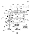
- FIG. 1 is a high-level, schematic diagram of a plasma chamber including a processing chamber having a slit valve door in accordance with one embodiment of the present invention
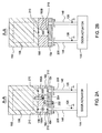
- Figures 2A-2E are cross-sectional views of exemplary embodiments of the slit valve door of Figure 1 ;
- Figures 3A-3C are equivalent electrical circuits of the slit valve doors depicted in Figures 2A-2E ;
- Figure 4 is a flow diagram illustrating a method for preventing arcing in a plasma chamber at a port exposed to plasma in accordance with one embodiment of the present invention.
- FIG. 1 is a high-level, schematic diagram of a plasma reactor 100 including a processing chamber 110 having a slit valve door 150 in accordance with one embodiment of the present invention.
- the plasma processing chamber 110 illustratively comprises a chamber body 102, a substrate pedestal 112 having an electrostatic chuck 113, liners 114, 116, a plasma-confining buffer 118, a showerhead 120 fluidly coupled to a gas panel 136, an upper electrode 122, and the slit valve door 150.
- Figures 2A-2E provide sectional views of exemplary embodiments of the slit valve door 150 of Figure 1 . To best understand the invention, the reader should simultaneously refer to Figures 1 and 2A-2E .
- the chamber body 102 is formed from a conductive material (for example, aluminum (Al)) and contains a substrate transfer port 104 for the entry and egress of substrates 124 processed in the reactor 100 (one substrate 124 disposed on the substrate chuck 113 is shown).
- a substrate transfer port 104 for the entry and egress of substrates 124 processed in the reactor 100 (one substrate 124 disposed on the substrate chuck 113 is shown).
- the chamber body 102, liners 114, 116, buffer 118, and, optionally, the showerhead 120 are coupled to a ground terminal 126 of the reactor 100.
- the liners 114, 116, buffer 118, and showerhead 120 may be grounded using a multi-point grounding technique.
- the upper electrode 122 through a matching network 128, is connected to a plasma power generator 130.
- the plasma power generator 130 and the bias power generator 134 are radio-frequency (RF) power supplies having operating frequencies of about 162MHz and 13.56 MHz, respectively.
- the plasma power generator 130 and the bias power generator 134 together or individually, produce plasma 106 (shown in phantom).
- the plasma 106 may be further controlled using optional steering coils and magnets (or electromagnets) (steering coils 138A, 138B and magnets 140A, 140B are shown).
- the processing reactor 100 also includes conventional systems and devices, which, in operation, facilitate execution and control of plasma processing of the substrates 124 in the reactor 100. Such systems are collectively shown herein as support systems 142.
- the reactor 100 may be an etch chamber employing a plasma for etching material used in fabrication of various integrated circuits.
- a plasma for etching material used in fabrication of various integrated circuits.
- One suitable etch reactor that may be adapted to benefit from the invention is an ENABLER ® plasma etch reactor available from Applied Materials, Inc., located in Santa Clara, California.
- the processing chamber 110 may have the plasma or bias generators operating at different frequencies, as well as having different means for producing the plasma, and adapted for performing plasma enhanced chemical vapor deposition or physical vapor deposition processes, among other plasma processes.
- the processing chamber 110 may have one or more external, internal, or remote inductive or capacitive RF plasma source or a microwave (MW) plasma source.
- MW microwave
- the slit valve door 150 provides a barrier between the interior of the chamber 110 and neighboring chambers that may be opened to allow substrate transfer.
- a door actuator 144 via at least one driving rod 146, moves the slit valve door 150 between open and closed positions.
- the slit valve door 150 is positioned in an upper, or closed, position (shown in Figure 1 ), where the door may provide a vacuum-tight seal of the substrate transfer port 104. Accordingly, when the slit valve door 150 is positioned in a lower, or open, position (not shown), the substrate 124 may be transferred through the substrate transfer port 104 into or out of the processing chamber 110 through a port 149 formed between or in one of the liners 114, 116.
- the slit valve door 150 may be spaced apart from adjacent portions of the door and the chamber body 102 defining gaps 148. During a plasma process, the plasma may extend through the port 149 of the liners 114, 116, and further through the substrate transfer port 104, to the slit valve door 150 and, sometimes, into the gaps 148.
- the slit valve door 150 includes a sealing panel 152, a driving panel 154, and a spacer 156.
- the spacer 156 is disposed between the panels 152, 154.
- the sealing panel 152 closes the substrate transfer port 104. In this position, the sealing panel 152 may be exposed to the plasma 106.
- Each of the panels 152, 154 is fabricated from a conductive material (for example, aluminum, stainless steel or other suitable metal), while the spacer 156 is fabricated from a dielectric material, such as a plastic, ceramic, polyimide, or other suitable dielectric material.
- the sealing panel 152 has a protective layer 158 (for example, silicon carbide (SiC) layer) that, in the sealed position, faces the interior of the processing chamber 110 through the substrate transfer port 104.
- the driving panel 154 is mechanically connected to one or more driving rods 146 of the door actuator 144.
- the driving rods 146 are fabricated from a conductive material (for example, metal or alloy) and electrically coupled to the driving panel 154 and the ground terminal 126 of the reactor 100, as shown in Figures 2A-2C , through a circuit component 160A, 160B or 160C.
- the driving rods 146 may be fabricated from a dielectric material (as shown) or be electrically isolated from the driving panel 154 (not shown in Figure 2D ).
- the sealing panel 152 is electrically coupled via the driving panel 154 to the ground terminal 126 through a separate electrical lead.
- a circuit component 160D may be disposed between the door 150 and ground 126 in a suitable location remote from the door 150, as shown in Figure 2E .
- the sealing panel 152 is electrically coupled to the ground terminal 126 through a separate electrical lead 198 having the circuit component 160D in series.
- the panels 152, 154 and the spacer 156 are mechanically coupled using fasteners 202, 204 (for example, screws, rivets, clamps or other coupling element).
- the fasteners 202, 204 (shown only in Figure 2A for clarity) are arranged to prevent electrical coupled between the panels 152, 154 through the fasteners 202, 204.
- the driving rods 146 may be connected to the driving panel 154 using conductive flanges 206 (as shown in Figures 2A-2B , 2D ) or nonconductive flanges 208 (as shown in Figure 2C ).
- the panels 152, 154 are electrically coupled together using one or more circuit components.
- the circuit components are depicts as 160A in the embodiment of Figure 2A , 160B in the embodiment of Figure 2B , and 160C in the embodiment of Figure 2C .
- the circuit components, now collectively referred to as components 160, are selected such that the ground path through the door 150 has a pre-determined impedance matching the excitation frequency F PL of the plasma 106.
- the components 160 may be alternatively selected such that the ground path through the door 150 has a pre-determined impedance offset from the excitation frequency F PL of the plasma 106 so that the potential difference influences the shape, position or other plasma characteristic, for example, to correct or create plasma asymmetries cause by other chamber or reactor components.
- the frequency F PL is an operating frequency of about 162 MHz of the plasma generator 130.
- the circuit components 160 are disposed in cavities 162 formed in the spacers 156. The cavities 162 are configured with terminals (not shown) to facility easy replacement and exchange of the circuit components 160.
- the slit valve door 150 includes the sealing panel 152 and, optionally, the driving panel 154.
- Each of the driving rods 146 includes portions 146 1 and 146 2 , which are separated using a dielectric spacer 214.
- the circuit component 160D are disposed in cavities 216 formed in the spacers 214.
- contact leads of the circuit components 160 may be connected to the respective elements of the slit valve door 150 or driving rods 146 using solder, binding or moveable contacts 210.
- contacts 210 include bayonet fittings, solder terminals, buses and the like.
- the sealing panel 152, driving panel 154 and driving rods 146 provide a short circuit (i.e., form a short-circuit path) at the excitation frequency F PL of the plasma, thereby suppressing plasma-induced arcing at the driving panel 154, substrate transfer port 104, and in the gaps 148.
- values of the circuit components 160 are selectively chosen to form the short circuit at the excitation frequency F PL .
- each circuit component may be selected to provide a short circuit at a respective frequency.
- FIGS 3A-3C depict equivalent electrical circuits 310, 320, 330 of the slit valve door 150 fabricated in accordance with embodiments of the present invention shown in Figures 2A-2E .
- the sealing panel 152 and conductive driving rods 146 represent to the plasma 106 capacitive and inductive impedances Z1 and Z4, respectively, while impedance Z3 of the driving panel 154 is about 0 (zero).
- the sealing panel 152 represents capacitive impedance Z1 to the plasma 106, while impedance Z3 of the driving panel 154 is about zero.
- the sealing panel 152 represents capacitive impedance Z1 to the plasma 106.
- circuit components 160A-160E may include inductor and/or other circuit components.
- values of the circuit components 160 may be determined experimentally, e.g., by selecting the components that provide suppression of the plasma-induced arcing at the slit valve door 150 or the substrate transfer port 104. Once the appropriate value of the capacitor or other circuit component 160 is determined, the door 150 (or rod) may be disassembled and a capacitor of the determined value may be installed in the cavity or other position along the door to ground path.
- Figure 4 is a flow diagram illustrating a method 400 for preventing arcing in a plasma chamber at a port exposed to plasma in accordance with one embodiment of the present invention.
- the method 400 may be performed using the plasma etch reactor 100 of Figure 1 , among other chambers adapted for performing plasma processes.
- the method 400 may be performed to tune other components of an plasma processing system to prevent arcing, or to reposition the plasma within the chamber to correct or create plasma asymmetry.
- the method 400 begins at step 410 when the plasma chamber is provided with a slit valve door adapted for sealing a substrate transfer port of the plasma chamber.
- the door is electrically coupled to ground.
- the door ground path includes at least one replaceable electrical component, such as a capacitor and/or inductor. It is also contemplated that the door ground path may alternatively include a tunable electrical component, wherein tunable component allows the impedance of the ground path to be adjusted. Examples of such doors are discussed above in reference to Figures 1 and 2A-2E .
- the electrical component of the ground path of the door is temporarily replace using conductive shunts.
- impedance of the door in the sealing position is measured to determine the impedance, together with the other components of the door ground path, required to provide a short circuit path at excitation frequency of the plasma.
- the impedance may be determined a network analyzer or experimentally, e.g., by literately choosing circuit components, such as capacitors and/or inductors, that suppress arcing at the door or substrate access port or create the desired plasma configuration.
- the conductive shunt is replaced with a circuit component having an impedance value selected such that the door ground path provides a short circuit path at excitation frequency of the plasma.
- the door suppresses plasma-induced arcing in proximity to the port exposed to the plasma.
- the method 400 ends. It is contemplated that the method 400 may be adapted to determine a door ground path impedance for use in tuning other components of the plasma processing chamber to prevent arcing, or to reposition the plasma within the chamber to correct or create plasma asymmetry.
- a method and apparatus controls plasma positing in a plasma processing chamber.
- the invention may be utilized to prevent arcing at substrate transfer ports or other components exposed to a plasma in the processing chamber, as well as to tune other components of the plasma processing chamber to prevent arcing, or to reposition the plasma within the chamber to correct or create plasma asymmetry.
Landscapes
- Physics & Mathematics (AREA)
- Engineering & Computer Science (AREA)
- Plasma & Fusion (AREA)
- Chemical & Material Sciences (AREA)
- Analytical Chemistry (AREA)
- Plasma Technology (AREA)
- Drying Of Semiconductors (AREA)
Abstract
A method and apparatus for preventing arcing at a port exposed to a plasma in a plasma chamber use circuit components causing a door sealing the port to provide a short circuit path at excitation frequency of the plasma. In one embodiment, the door is a slit valve door sealing a substrate transfer port of an etch chamber.
Description
- Embodiments of the present invention generally relate to plasma processing chambers used in the semiconductor industry to manufacture integrated circuits and, more specifically, to methods and apparatuses for preventing arcing or undesired plasma glows in plasma processing chambers.
- In the manufacture of integrated circuits (ICs), many processing steps are performed using plasma chambers, such as plasma etch chambers, plasma enhanced chemical vapor deposition (PECVD) chambers, reactive ion etch (RIE) chambers, electron cyclotron resonance (ECR) chambers, and the like. Plasma-induced arcing in such chambers is a phenomenon that detrimentally affects yield and, specifically, causes particle contamination and uniformity of the fabricated features and devices of the lCs.
- One particular region vulnerable to plasma-induced arcing or plasma glows is the region adjacent to slit valve doors utilized to seal substrate transfer ports. In particular, plasma arcing is often observed in proximity to substrate transfer ports and, specifically, at doors used for sealing such ports during plasma processing of substrates in the respective chambers. Generally, severity of plasma arcing in these regions increases with excitation frequency of the plasma.
- Unless the plasma is surrounded by surfaces representing a short circuit at excitation frequency of the plasma, arcing may occur between the plasma and those inner surfaces of a processing chamber. While many components of the processing chamber can be sufficiently well grounded using, for example, multi-point grounding techniques, preventing plasma formation at or near the slit valve door has remained a challenge.
- Therefore, there is a need for improvements in the prevention of undesired plasma formation at chamber ports.
- A method and apparatus for preventing arcing at a port exposed to a plasma in a plasma processing chamber are provided. In one particular embodiment, the port is a substrate transfer port of the chamber.
- One aspect of the present invention is a method for fabricating a door of a slit valve. In one embodiment, the method includes fabricating a door which panels are electrically coupled together using one or more circuit components that cause the door to provide, at excitation frequency of a plasma, a short circuit. In another embodiment, the circuit components are disposed in elements of an actuator of the door.
- Another aspect of the present invention is a slit valve door fabricated using the inventive method. The door may be used in a plasma chamber to suppress plasma-induced arcing in proximity to substrate transfer ports and the door itself.
- Yet another aspect of the present invention is a plasma processing chamber for fabricating integrated circuits on substrates. The processing includes a substrate transfer port that, during plasma processing, is selectively sealed using the inventive door assembly.
- In still another embodiment, a processing chamber is provided that has a component that is coupled to ground through a circuit having an inductance selected to influence the shape and/or position of a plasma within the processing chamber. In one embodiment, the component may be a slit valve door. As such, the plasma may be influenced by the door to correct or reposition the plasma in relation to a substrate support, thus compensating for other electrical or conductive (pumping) asymmetries of the chamber.
- So that the manner in which the above recited features of the present invention can be understood in detail, a more particular description of the invention, briefly summarized above, may be had by reference to embodiments, some of which are illustrated in the appended drawings. It is to be noted, however, that the appended drawings illustrate only typical embodiments of this invention and are therefore not to be considered limiting of its scope, for the invention may admit to other equally effective embodiments.
-
Figure 1 is a high-level, schematic diagram of a plasma chamber including a processing chamber having a slit valve door in accordance with one embodiment of the present invention; -
Figures 2A-2E are cross-sectional views of exemplary embodiments of the slit valve door ofFigure 1 ; -
Figures 3A-3C are equivalent electrical circuits of the slit valve doors depicted inFigures 2A-2E ; and -
Figure 4 is a flow diagram illustrating a method for preventing arcing in a plasma chamber at a port exposed to plasma in accordance with one embodiment of the present invention. - To facilitate understanding, identical reference numerals have been used, where possible, to designate identical elements that are common to the figures, except that suffixes may be added, when appropriate, to differentiate such elements. The images in the drawings are simplified for illustrative purposes and are not depicted to scale. It is contemplated that features or steps of one embodiment may be beneficially incorporated in other embodiments without further recitation.
-
Figure 1 is a high-level, schematic diagram of aplasma reactor 100 including aprocessing chamber 110 having aslit valve door 150 in accordance with one embodiment of the present invention. In the depicted embodiment, theplasma processing chamber 110 illustratively comprises achamber body 102, asubstrate pedestal 112 having anelectrostatic chuck 113,liners confining buffer 118, ashowerhead 120 fluidly coupled to agas panel 136, anupper electrode 122, and theslit valve door 150. -
Figures 2A-2E provide sectional views of exemplary embodiments of theslit valve door 150 ofFigure 1 . To best understand the invention, the reader should simultaneously refer toFigures 1 and2A-2E . - The
chamber body 102 is formed from a conductive material (for example, aluminum (Al)) and contains asubstrate transfer port 104 for the entry and egress ofsubstrates 124 processed in the reactor 100 (onesubstrate 124 disposed on thesubstrate chuck 113 is shown). Conventionally, thechamber body 102,liners buffer 118, and, optionally, theshowerhead 120 are coupled to aground terminal 126 of thereactor 100. In particular, theliners buffer 118, andshowerhead 120 may be grounded using a multi-point grounding technique. - The
upper electrode 122, through amatching network 128, is connected to aplasma power generator 130. Thesubstrate pedestal 112, through amatching network 132, is connected to abias power generator 134. In one exemplary embodiment, theplasma power generator 130 and thebias power generator 134 are radio-frequency (RF) power supplies having operating frequencies of about 162MHz and 13.56 MHz, respectively. - During processing a
substrate 124, theplasma power generator 130 and thebias power generator 134, together or individually, produce plasma 106 (shown in phantom). In the depicted embodiment, theplasma 106 may be further controlled using optional steering coils and magnets (or electromagnets) (steering coils magnets processing reactor 100 also includes conventional systems and devices, which, in operation, facilitate execution and control of plasma processing of thesubstrates 124 in thereactor 100. Such systems are collectively shown herein assupport systems 142. - The
reactor 100 may be an etch chamber employing a plasma for etching material used in fabrication of various integrated circuits. One suitable etch reactor that may be adapted to benefit from the invention is an ENABLER® plasma etch reactor available from Applied Materials, Inc., located in Santa Clara, California. In other embodiments, theprocessing chamber 110 may have the plasma or bias generators operating at different frequencies, as well as having different means for producing the plasma, and adapted for performing plasma enhanced chemical vapor deposition or physical vapor deposition processes, among other plasma processes. In one embodiment, theprocessing chamber 110 may have one or more external, internal, or remote inductive or capacitive RF plasma source or a microwave (MW) plasma source. Various types of the plasma chambers that may benefit from the invention are commercially available from Applied Materials Inc., among other plasma processing equipment manufacturers. - The
slit valve door 150 provides a barrier between the interior of thechamber 110 and neighboring chambers that may be opened to allow substrate transfer. In operation, adoor actuator 144, via at least onedriving rod 146, moves theslit valve door 150 between open and closed positions. During plasma processing in theprocessing chamber 110, theslit valve door 150 is positioned in an upper, or closed, position (shown inFigure 1 ), where the door may provide a vacuum-tight seal of thesubstrate transfer port 104. Accordingly, when theslit valve door 150 is positioned in a lower, or open, position (not shown), thesubstrate 124 may be transferred through thesubstrate transfer port 104 into or out of theprocessing chamber 110 through aport 149 formed between or in one of theliners - The
slit valve door 150 may be spaced apart from adjacent portions of the door and thechamber body 102 defininggaps 148. During a plasma process, the plasma may extend through theport 149 of theliners substrate transfer port 104, to theslit valve door 150 and, sometimes, into thegaps 148. - In one embodiment, the
slit valve door 150 includes asealing panel 152, adriving panel 154, and aspacer 156. Thespacer 156 is disposed between thepanels sealing panel 152 closes thesubstrate transfer port 104. In this position, thesealing panel 152 may be exposed to theplasma 106. - Each of the
panels spacer 156 is fabricated from a dielectric material, such as a plastic, ceramic, polyimide, or other suitable dielectric material. In one embodiment, the sealingpanel 152 has a protective layer 158 (for example, silicon carbide (SiC) layer) that, in the sealed position, faces the interior of theprocessing chamber 110 through thesubstrate transfer port 104. - The driving
panel 154 is mechanically connected to one ormore driving rods 146 of thedoor actuator 144. In some embodiments, the drivingrods 146 are fabricated from a conductive material (for example, metal or alloy) and electrically coupled to the drivingpanel 154 and theground terminal 126 of thereactor 100, as shown inFigures 2A-2C , through acircuit component - In an alternate embodiment shown in
Figure 2D , the drivingrods 146 may be fabricated from a dielectric material (as shown) or be electrically isolated from the driving panel 154 (not shown inFigure 2D ). In this embodiment, the sealingpanel 152 is electrically coupled via the drivingpanel 154 to theground terminal 126 through a separate electrical lead. - In another alternate embodiment shown in
Figure 2E , acircuit component 160D may be disposed between thedoor 150 andground 126 in a suitable location remote from thedoor 150, as shown inFigure 2E . In this embodiment, the sealingpanel 152 is electrically coupled to theground terminal 126 through a separateelectrical lead 198 having thecircuit component 160D in series. - Referring to
Figures 2A-2D , illustratively, thepanels spacer 156 are mechanically coupled usingfasteners 202, 204 (for example, screws, rivets, clamps or other coupling element). In the embodiments depicted inFigures 2A-C , thefasteners 202, 204 (shown only inFigure 2A for clarity) are arranged to prevent electrical coupled between thepanels fasteners rods 146 may be connected to the drivingpanel 154 using conductive flanges 206 (as shown inFigures 2A-2B ,2D ) or nonconductive flanges 208 (as shown inFigure 2C ). - In the embodiments depicted in
Figures 2A-C , thepanels Figure 2A , 160B in the embodiment ofFigure 2B , and 160C in the embodiment ofFigure 2C . The circuit components, now collectively referred to ascomponents 160, are selected such that the ground path through thedoor 150 has a pre-determined impedance matching the excitation frequency FPL of theplasma 106. It is also contemplated that thecomponents 160 may be alternatively selected such that the ground path through thedoor 150 has a pre-determined impedance offset from the excitation frequency FPL of theplasma 106 so that the potential difference influences the shape, position or other plasma characteristic, for example, to correct or create plasma asymmetries cause by other chamber or reactor components. In one example, the frequency FPL is an operating frequency of about 162 MHz of theplasma generator 130. In embodiments shown inFigures 1 ,2A-2C , thecircuit components 160 are disposed incavities 162 formed in thespacers 156. Thecavities 162 are configured with terminals (not shown) to facility easy replacement and exchange of thecircuit components 160. - In an alternative embodiment depicted in
Figure 2D , theslit valve door 150 includes the sealingpanel 152 and, optionally, the drivingpanel 154. Each of the drivingrods 146 includesportions dielectric spacer 214. In this embodiment, thecircuit component 160D are disposed incavities 216 formed in thespacers 214. - Referring collectively to the embodiments depicted in
Figures 2A-D , contact leads of thecircuit components 160 may be connected to the respective elements of theslit valve door 150 or drivingrods 146 using solder, binding ormoveable contacts 210. Examples ofcontacts 210 include bayonet fittings, solder terminals, buses and the like. Together with thecircuit components 160, the sealingpanel 152, drivingpanel 154 and drivingrods 146 provide a short circuit (i.e., form a short-circuit path) at the excitation frequency FPLof the plasma, thereby suppressing plasma-induced arcing at the drivingpanel 154,substrate transfer port 104, and in thegaps 148. In particular, values of thecircuit components 160 are selectively chosen to form the short circuit at the excitation frequency FPL. In embodiments wherein more than one plasma excitation frequency is utilized, each circuit component may be selected to provide a short circuit at a respective frequency. -
Figures 3A-3C depict equivalentelectrical circuits slit valve door 150 fabricated in accordance with embodiments of the present invention shown inFigures 2A-2E . Referring toFigure 3A andFigures 2A-2C , during plasma processing, the sealingpanel 152 and conductive drivingrods 146 represent to theplasma 106 capacitive and inductive impedances Z1 and Z4, respectively, while impedance Z3 of the drivingpanel 154 is about 0 (zero). In the embodiments ofFigures 2A-2C , theslit valve door 150 forms a short circuit at the excitation frequency FPL whencomponents 160A (shown inFigure 2A ) or asingle component Figures 2B-2C ) are capacitors, which impedances are selected such that, at the frequency FPL, impedance Z310 of an equivalentelectrical circuit 310 is equal to or about zero, i.e.,
- Referring to
Figure 3B andFigure 2D , during plasma processing, the sealingpanel 152 represents capacitive impedance Z1 to theplasma 106, while impedance Z3 of the drivingpanel 154 is about zero. Theslit valve door 150 forms a short circuit at the excitation frequency FPL whencircuit components 160D is an capacitor, which capacitance is selected such that, at the frequency FPL, impedance Z320 of an equivalentelectrical circuit 320 is equal to or about zero, i.e.,
- Referring to
Figure 3C andFigure 2E , during plasma processing, the sealingpanel 152 represents capacitive impedance Z1 to theplasma 106. Theslit valve door 150 forms a short circuit at the excitation frequency FPL when circuit components 160E is an capacitor, which capacitance is selected such that, at the frequency FPL, impedance Z320 of an equivalentelectrical circuit 320 is equal to or about zero, i.e.,
- Values of the capacitors of the
circuit components 160A-160E may be determined by measuring impedance of the respectiveslit valve doors 150 where thecircuit components 160 are temporarily replaced with shunts. Such measurements can be performed using, for example, a network analyzer which probe is coupled, through thesubstrate transfer port 104, to the sealingpanel 152. The results of these measurements allow to define properties S1 = Z1 + Z3 + Z4 and S2 = Z1 + Z3 in the equations (1) and (2), respectively. Then, values of thecapacitors 160A-160C may be determined by resolving the equation:
- It is contemplated that the
circuit components 160A-160E may include inductor and/or other circuit components. - Alternatively, during plasma processing of non-product substrates, values of the
circuit components 160 may be determined experimentally, e.g., by selecting the components that provide suppression of the plasma-induced arcing at theslit valve door 150 or thesubstrate transfer port 104. Once the appropriate value of the capacitor orother circuit component 160 is determined, the door 150 (or rod) may be disassembled and a capacitor of the determined value may be installed in the cavity or other position along the door to ground path. -
Figure 4 is a flow diagram illustrating amethod 400 for preventing arcing in a plasma chamber at a port exposed to plasma in accordance with one embodiment of the present invention. One skilled in the art will readily appreciate that themethod 400 may be performed using theplasma etch reactor 100 ofFigure 1 , among other chambers adapted for performing plasma processes. One skilled in the art will also readily appreciate that themethod 400 may be performed to tune other components of an plasma processing system to prevent arcing, or to reposition the plasma within the chamber to correct or create plasma asymmetry. - The
method 400 begins atstep 410 when the plasma chamber is provided with a slit valve door adapted for sealing a substrate transfer port of the plasma chamber. The door is electrically coupled to ground. The door ground path includes at least one replaceable electrical component, such as a capacitor and/or inductor. It is also contemplated that the door ground path may alternatively include a tunable electrical component, wherein tunable component allows the impedance of the ground path to be adjusted. Examples of such doors are discussed above in reference toFigures 1 and2A-2E . - At
step 420, the electrical component of the ground path of the door is temporarily replace using conductive shunts. Then, atstep 430, impedance of the door in the sealing position is measured to determine the impedance, together with the other components of the door ground path, required to provide a short circuit path at excitation frequency of the plasma. The impedance may be determined a network analyzer or experimentally, e.g., by literately choosing circuit components, such as capacitors and/or inductors, that suppress arcing at the door or substrate access port or create the desired plasma configuration. - At
step 440, the conductive shunt is replaced with a circuit component having an impedance value selected such that the door ground path provides a short circuit path at excitation frequency of the plasma. During plasma processing, the door suppresses plasma-induced arcing in proximity to the port exposed to the plasma. Upon completion ofstep 440, themethod 400 ends. It is contemplated that themethod 400 may be adapted to determine a door ground path impedance for use in tuning other components of the plasma processing chamber to prevent arcing, or to reposition the plasma within the chamber to correct or create plasma asymmetry. - Thus, a method and apparatus has been provided controls plasma positing in a plasma processing chamber. Advantageously, the invention may be utilized to prevent arcing at substrate transfer ports or other components exposed to a plasma in the processing chamber, as well as to tune other components of the plasma processing chamber to prevent arcing, or to reposition the plasma within the chamber to correct or create plasma asymmetry.
- Although the invention herein has been described with reference to particular exemplary embodiments, it is to be understood that these embodiments are merely illustrative of the principles and applications of the present invention. Therefore, numerous modifications may be made to these embodiments and other arrangements may be devised without departing from the spirit and scope of the present invention, and the scope thereof is defined by the appended claims.
Claims (20)
- A plasma processing chamber, comprising:a chamber body having a substrate access port;an element for coupling energy to a plasma formed within the chamber;a chamber component exposed to a region within the chamber body in which the plasma is formed; anda ground path coupling the chamber component to ground, the ground path comprising at least one of a tunable or replaceable circuit component selected in response to an excitation frequency of the plasma and providing a predefined impedance value between the chamber component and ground.
- A plasma processing chamber, comprising:a chamber body having a substrate access port;a door positionable to close the substrate access port, the door having a face exposed to a region within the chamber body in which a plasma is formed; anda ground path coupling the door to ground, the ground path comprising at least one of a tunable or replaceable circuit component selected in response to an excitation frequency of the plasma and providing a predefined impedance value between the door and ground.
- The processing chamber of claim 2, wherein the circuit component further comprises:at least one of a capacitor or an inductor.
- The processing chamber of claim 2, wherein the circuit component is disposed in the door.
- The processing chamber of claim 2, wherein the door further comprises:a sealing panel positionable to close the access port;a driving panel coupled to the sealing panel; anda dielectric spacer electrically isolating the driving panel from and sealing panel, the spacer housing the circuit component, wherein the circuit component electrically couples the driving panel to the sealing panel.
- The processing chamber of claim 5, wherein the driving panel is coupled to ground.
- The processing chamber of claim 2, wherein the circuit component is remote from the door.
- The processing chamber of claim 7 further comprising:an actuator; anda rod coupling the actuator to the door, wherein the circuit component is coupled in series with the rod.
- The processing chamber of claim 7, wherein the rod is coupled to ground.
- The processing chamber of claim 7, wherein the rod further comprises:a cavity having the circuit component disposed therein.
- The processing chamber of claim 7 further comprising:a lead coupled to the door, the lead having the circuit component coupled in series.
- A plasma processing chamber, comprising:a chamber body having a substrate access port;a door positionable to close the substrate access port, the door having a face exposed to a region within the chamber body in which a plasma is formed;a rod;an actuator coupled to the door by the rod, the actuator controlling the position of the door; anda ground path coupling the door to ground, the ground path comprising replaceable circuit component disposed in at least one of the rod or door.
- The processing chamber of claim 12, wherein the circuit component further comprises:at least one of a capacitor or an inductor.
- A method for preventing arcing at a door sealing a port exposed to a plasma in a plasma chamber, comprising:providing a plasma chamber having a slit valve door adapted for sealing a substrate transfer port of the plasma chamber, the door being electrically coupled to ground through a ground path;measuring an impedance of the door in a transfer port sealing position to determine an impedance required to provide a short circuit through the ground path at excitation frequency of a plasma formed in the plasma chamber; andcoupling in series, with the ground path, a circuit component having an impedance value substantially equal to the determined impedance.
- The method of claim 14, wherein coupling the circuit component in series with the ground path further comprises:replacing a conductive shunt used during the measuring step with the electrical component.
- The method of claim 14, wherein coupling the circuit component in series with the ground path further comprises:installing the electrical component in the door.
- The method of claim 14, wherein coupling the circuit component in series with the ground path further comprises:installing the electrical component in a rod coupling the door to an actuator.
- The method of claim 14, wherein coupling the circuit component in series with the ground path further comprises:installing the electrical component in series with a lead coupling the door to door, the electrical component installed in a position remote from the door.
- The method of claim 14, wherein coupling the circuit component in series with the ground path further comprises:installing a first electrical component in a first parallel branch of the ground path selected to provide a short circuit at a first plasma excitation frequency; andinstalling a second electrical component in a second parallel branch of the ground path selected to provide a short circuit at a second plasma excitation frequency.
- The method of claim 14, wherein measuring the impedance further comprises:determining the impedance based on data acquired using a network analyzer or using experimental data.
Applications Claiming Priority (1)
| Application Number | Priority Date | Filing Date | Title |
|---|---|---|---|
| US11/610,709 US7943006B2 (en) | 2006-12-14 | 2006-12-14 | Method and apparatus for preventing arcing at ports exposed to a plasma in plasma processing chambers |
Publications (1)
| Publication Number | Publication Date |
|---|---|
| EP1933364A2 true EP1933364A2 (en) | 2008-06-18 |
Family
ID=39166337
Family Applications (1)
| Application Number | Title | Priority Date | Filing Date |
|---|---|---|---|
| EP07122850A Withdrawn EP1933364A2 (en) | 2006-12-14 | 2007-12-11 | Method and apparatus for preventing arcing at ports exposed to a plasma in plasma processing chambers |
Country Status (7)
| Country | Link |
|---|---|
| US (1) | US7943006B2 (en) |
| EP (1) | EP1933364A2 (en) |
| JP (1) | JP5300256B2 (en) |
| KR (1) | KR100942071B1 (en) |
| CN (1) | CN101207014A (en) |
| SG (1) | SG144071A1 (en) |
| TW (1) | TWI359435B (en) |
Cited By (1)
| Publication number | Priority date | Publication date | Assignee | Title |
|---|---|---|---|---|
| CN111213221A (en) * | 2017-10-05 | 2020-05-29 | 应用材料公司 | Split slit gasket door |
Families Citing this family (17)
| Publication number | Priority date | Publication date | Assignee | Title |
|---|---|---|---|---|
| US20090230089A1 (en) * | 2008-03-13 | 2009-09-17 | Kallol Bera | Electrical control of plasma uniformity using external circuit |
| KR20140048752A (en) * | 2012-10-16 | 2014-04-24 | 삼성전자주식회사 | Slit valve unit and film forming apparatus having the same |
| KR102354975B1 (en) | 2015-06-18 | 2022-01-25 | 삼성디스플레이 주식회사 | Plasma enhanced chemical vapor deposition device and display apparatus using the same |
| US11430635B2 (en) * | 2018-07-27 | 2022-08-30 | Eagle Harbor Technologies, Inc. | Precise plasma control system |
| US11227745B2 (en) | 2018-08-10 | 2022-01-18 | Eagle Harbor Technologies, Inc. | Plasma sheath control for RF plasma reactors |
| US11004660B2 (en) | 2018-11-30 | 2021-05-11 | Eagle Harbor Technologies, Inc. | Variable output impedance RF generator |
| WO2018039055A1 (en) * | 2016-08-22 | 2018-03-01 | Applied Materials, Inc. | Door seal for vacuum chamber |
| US11532457B2 (en) | 2018-07-27 | 2022-12-20 | Eagle Harbor Technologies, Inc. | Precise plasma control system |
| US11810761B2 (en) | 2018-07-27 | 2023-11-07 | Eagle Harbor Technologies, Inc. | Nanosecond pulser ADC system |
| US12456604B2 (en) | 2019-12-24 | 2025-10-28 | Eagle Harbor Technologies, Inc. | Nanosecond pulser RF isolation for plasma systems |
| EP4486072A3 (en) | 2019-12-24 | 2025-04-09 | Eagle Harbor Technologies, Inc. | Nanosecond pulser rf isolation for plasma systems |
| KR102814256B1 (en) * | 2020-05-29 | 2025-05-30 | 주성엔지니어링(주) | Substrate Processing Apparatus |
| US11967484B2 (en) | 2020-07-09 | 2024-04-23 | Eagle Harbor Technologies, Inc. | Ion current droop compensation |
| CN114525498B (en) * | 2022-03-07 | 2022-11-01 | 苏州迈为科技股份有限公司 | Droop cover plate and Plasma Enhanced Chemical Vapor Deposition (PECVD) equipment with same |
| US11824542B1 (en) | 2022-06-29 | 2023-11-21 | Eagle Harbor Technologies, Inc. | Bipolar high voltage pulser |
| JP7833099B2 (en) | 2022-09-29 | 2026-03-18 | イーグル ハーバー テクノロジーズ,インク. | High-voltage plasma control |
| US12176190B2 (en) * | 2023-03-07 | 2024-12-24 | Applied Materials, Inc. | Arc management algorithm of RF generator and match box for CCP plasma chambers |
Family Cites Families (10)
| Publication number | Priority date | Publication date | Assignee | Title |
|---|---|---|---|---|
| US6192827B1 (en) | 1998-07-03 | 2001-02-27 | Applied Materials, Inc. | Double slit-valve doors for plasma processing |
| JP3902878B2 (en) * | 1998-11-30 | 2007-04-11 | キヤノン株式会社 | Functional deposition film forming equipment |
| US6390448B1 (en) * | 2000-03-30 | 2002-05-21 | Lam Research Corporation | Single shaft dual cradle vacuum slot valve |
| AU2002227418A1 (en) * | 2001-01-22 | 2002-08-06 | Tokyo Electron Limited | Vertically translatable chuck assembly and method for a plasma reactor system |
| JP4051209B2 (en) * | 2001-02-02 | 2008-02-20 | キヤノンアネルバ株式会社 | High frequency plasma processing apparatus and high frequency plasma processing method |
| JP4819244B2 (en) * | 2001-05-15 | 2011-11-24 | 東京エレクトロン株式会社 | Plasma processing equipment |
| JP2003163206A (en) * | 2001-11-28 | 2003-06-06 | Tokyo Electron Ltd | Plasma processing apparatus, plasma processing method, and multi-chamber system |
| JP4030766B2 (en) | 2002-01-30 | 2008-01-09 | アルプス電気株式会社 | Plasma processing equipment |
| US6841943B2 (en) * | 2002-06-27 | 2005-01-11 | Lam Research Corp. | Plasma processor with electrode simultaneously responsive to plural frequencies |
| JP4141234B2 (en) * | 2002-11-13 | 2008-08-27 | キヤノンアネルバ株式会社 | Plasma processing equipment |
-
2006
- 2006-12-14 US US11/610,709 patent/US7943006B2/en not_active Expired - Fee Related
-
2007
- 2007-12-11 EP EP07122850A patent/EP1933364A2/en not_active Withdrawn
- 2007-12-12 SG SG200718606-7A patent/SG144071A1/en unknown
- 2007-12-12 JP JP2007321023A patent/JP5300256B2/en not_active Expired - Fee Related
- 2007-12-14 TW TW096147997A patent/TWI359435B/en not_active IP Right Cessation
- 2007-12-14 CN CNA2007101959754A patent/CN101207014A/en active Pending
- 2007-12-14 KR KR1020070130951A patent/KR100942071B1/en not_active Expired - Fee Related
Cited By (2)
| Publication number | Priority date | Publication date | Assignee | Title |
|---|---|---|---|---|
| CN111213221A (en) * | 2017-10-05 | 2020-05-29 | 应用材料公司 | Split slit gasket door |
| CN111213221B (en) * | 2017-10-05 | 2022-11-25 | 应用材料公司 | Split slit gasket door |
Also Published As
| Publication number | Publication date |
|---|---|
| KR100942071B1 (en) | 2010-02-12 |
| US7943006B2 (en) | 2011-05-17 |
| SG144071A1 (en) | 2008-07-29 |
| KR20080055729A (en) | 2008-06-19 |
| TWI359435B (en) | 2012-03-01 |
| JP2008171807A (en) | 2008-07-24 |
| US20080141940A1 (en) | 2008-06-19 |
| TW200845081A (en) | 2008-11-16 |
| JP5300256B2 (en) | 2013-09-25 |
| CN101207014A (en) | 2008-06-25 |
Similar Documents
| Publication | Publication Date | Title |
|---|---|---|
| EP1933364A2 (en) | Method and apparatus for preventing arcing at ports exposed to a plasma in plasma processing chambers | |
| US10854492B2 (en) | Edge ring assembly for improving feature profile tilting at extreme edge of wafer | |
| EP1840937B1 (en) | Plasma processing apparatus and plasma processing method | |
| US8138445B2 (en) | Plasma processing apparatus and plasma processing method | |
| US7199327B2 (en) | Method and system for arc suppression in a plasma processing system | |
| US7086347B2 (en) | Apparatus and methods for minimizing arcing in a plasma processing chamber | |
| KR102770109B1 (en) | Adjustment method for filter unit and plasma processing apparatus | |
| JP5566970B2 (en) | Apparatus and method for actively controlling RF peak-to-peak voltage of inductively coupled plasma etching apparatus | |
| US20120270406A1 (en) | Cleaning method of plasma processing apparatus and plasma processing method | |
| US6422173B1 (en) | Apparatus and methods for actively controlling RF peak-to-peak voltage in an inductively coupled plasma etching system | |
| JP7059064B2 (en) | Plasma processing equipment | |
| KR20060087474A (en) | Process Kits for Use in Plasma Process Chambers | |
| US11094509B2 (en) | Plasma processing apparatus | |
| CN119833382A (en) | Dual-frequency direct-drive inductively coupled plasma source | |
| CN101188189A (en) | Confinement Baffles and Flow Equalizers for Enhanced Magnetic Control of Radial Plasma Distribution | |
| EP1269512B1 (en) | Inductively coupled plasma etching apparatus with active control of RF peak-to-peak voltage | |
| JP2001345311A (en) | Device and method for actively controlling rf peak-to- peak voltage of inductively coupled plasma etching system | |
| KR20230102034A (en) | Substrate processing apparatus, harmonics control unit and harmonics contol method | |
| JP2015207562A (en) | Plasma processing device and plasma processing method | |
| JP6002365B2 (en) | Plasma processing apparatus and plasma processing method | |
| KR102874571B1 (en) | Self-plasma chamber's visible window contamination suppression and removal system | |
| KR200426498Y1 (en) | Process Kits for Use in Plasma Process Chambers |
Legal Events
| Date | Code | Title | Description |
|---|---|---|---|
| PUAI | Public reference made under article 153(3) epc to a published international application that has entered the european phase |
Free format text: ORIGINAL CODE: 0009012 |
|
| AK | Designated contracting states |
Kind code of ref document: A2 Designated state(s): AT BE BG CH CY CZ DE DK EE ES FI FR GB GR HU IE IS IT LI LT LU LV MC MT NL PL PT RO SE SI SK TR |
|
| AX | Request for extension of the european patent |
Extension state: AL BA HR MK RS |
|
| STAA | Information on the status of an ep patent application or granted ep patent |
Free format text: STATUS: THE APPLICATION IS DEEMED TO BE WITHDRAWN |
|
| 18D | Application deemed to be withdrawn |
Effective date: 20100701 |